
Graphene Oxide-Coated Metal–Insulator–Metal SERS Substrates for Trace Melamine Detection
by

Zhenming Wang
1, 
Jianxun Liu
1,*,
Jiawei Wang
1,
Zongjun Ma
1,
Delai Kong
1,
Shouzhen Jiang
2,
Dan Luo
1 and
Yan Jun Liu
1,* 1
Department of Electrical and Electronic Engineering, Southern University of Science and Technology, Shenzhen 518055, China
2
Provincial Key Laboratory of Optics and Photonic Device, School of Physics and Electronics, Shandong Normal University, Jinan 250014, China
*
Authors to whom correspondence should be addressed.
Nanomaterials 2022, 12(7), 1202; https://doi.org/10.3390/nano12071202
Submission received: 17 February 2022
/
Revised: 27 March 2022
/
Accepted: 31 March 2022
/
Published: 3 April 2022
Abstract
:Surface-enhanced Raman spectroscopy (SERS) has long been an ultrasensitive technique for trace molecule detection. However, the development of a sensitive, stable, and reproducible SERS substrate is still a challenge for practical applications. Here, we demonstrate a cost-effective, centimeter-sized, and highly reproducible SERS substrate using the nanosphere lithography technique. It consists of a hexagonally packed Ag metasurface on a SiO2/Au/Si substrate. A seconds-lasting etching process of a self-assembled nanosphere mask manipulates the geometry of the deposited Ag metasurface on the SiO2/Au/Si substrate, which attains the wavelength matching between the optical absorbance of the Ag/SiO2/Au/Si substrate and the excitation laser wavelength as well as the enhancement of Raman signals. By spin-coating a thin layer of graphene oxide on the substrate, a SERS performance with 1.1 × 10⁵ analytical enhancement factor and a limit of detection of 10−9 M for melamine is achieved. Experimental results reveal that our proposed strategy could provide a promising platform for SERS-based rapid trace detection in food safety control and environmental monitoring.
1. Introduction
In recent years, the surface-enhanced Raman spectroscopy (SERS) technique for the detection of dangerous substances in small volumes and extremely low concentrations has attracted extensive interest [1,2,3,4]. As known, SERS can provide single-molecular sensitivity [5,6,7,8,9,10], label-free detection [11,12,13], and high-throughput screening of a huge number of samples [14,15], which is well suited for on-site trace detection and identification [16,17,18]. Among numerous theoretical and experimental reports on SERS substrates [16,17,18,19,20,21,22,23], there are three main strategies to enhance the Raman signal intensity and decrease the detection limit, including enhancing the absorption of incident light [19,20,21,22], amplifying the far-field radiation of Raman scattering signals [23,24], and increasing the attachment of the targeted substances [25,26]. A universal approach to enhancing absorption of the excitation laser and Raman signals is to construct a substrate composed of dense metal nanostructures [27,28,29]. These nanostructures have not only large optical absorption cross sections but also numerous “hot spots” produced by the localized surface plasmon resonance (LSPR) to enhance the far-field radiation. Large Raman signal enhancement has been achieved in some SERS substrates with randomly dispersed metal nanostructures [21,30]. However, how to increase the absorption of the excitation laser has yet been received enough attention. A good way to achieve a SERS substrate with specific wavelength absorption is to artificially design plasmonic metasurfaces [22,29,31,32], which are a periodic arrangement of subwavelength meta-atoms with special shapes, such as nanodisks, nanopillars, nanogrids, etc. [33,34,35,36,37,38].
Among numerous kinds of plasmonic nanostructures, nanobowties have been demonstrated to achieve relatively large Raman signal enhancement [34]. In addition, the choice of metal materials will also affect the Raman enhancement. For the case of 532 nm excitation laser, silver nanostructures have a smaller photothermal effect than gold ones, leading to a larger enhancement factor [35,38]. Besides silver, other materials such as aluminum, lead, and platinum are also good choices, but silver could be the best choice with a much easier fabrication process [39,40,41,42]. A detection limit down to 10−16 M for Rhodamine 6G has been reported by silver metasurfaces formatted with nanobowties [35]. Additionally, it is worth noting that the reduced photothermal effect could help avoid damage to the analytes during the measurement process [43].
As a well-known poisoning additive, melamine is sometimes illegally adulterated with food products in order to increase the apparent protein content. Ingestion of melamine may cause reproductive damage, kidney stones/failures, and bladder cancer. In adulterated milk products, melamine concentrations could be as high as ~3300 ppm, far exceeding the safety limit of 1 ppm (~7.9 × 10⁻⁶ M), hence posing an extreme danger to consumers. Therefore, rapid and unambiguous detection of trace amounts of melamine in food products is of paramount importance. To counteract the adverse effects of melamine, various analytical techniques based on SERS for detecting it in dairy and food products have been developed [44,45,46,47]. For example, in 2016, Dong et al. [44] used polythymine aptamer-modified Au nanoparticles to decrease the limit of detection down to 8 × 10⁻¹² M for melamine with the SERS effect. Li and co-workers [45] synthesized a monolayer film with Ag nanoparticles to realize a SERS effect on melamine with a limit of detection near 3 × 10⁻¹³ M. Such SERS substrates are characterized by the formation of a sufficient number of hot spots near or between nanoparticles to achieve the strong SERS effect. Huang and co-workers [46] demonstrated the low limit of detection of 1×10⁻¹⁶ M by using Ag nanoparticles decorated with Zinc oxide/Silicon heterostructured nanomace arrays as a SERS substrate. The large-area detection for extremely low concentration is realized; however, the SERS substrate fabrication process is very complicated and time-consuming. Kundan et al. [47] fabricated an Au nanorod array with a focused ion beam (FIB) and achieved the detection limit of 1 × 10⁻¹² M for melamine. Although the low limit of detection for melamine is also achieved in a large area, the preparation processes are greatly dependent on precision nanofabrication techniques, such as electron beam lithography (EBL) and FIB, leading to complicated and costly fabrication. Therefore, it is still in high demand to develop large-area, uniform SERS substrate with a simple and cost-effective fabrication technique. More importantly, there is no artificially designed structure to purposely investigate the effect of the characteristic absorption of excitation light on SERS signal enhancement.
Self-assembly-based nanosphere lithography (NSL) is a simple, cost-effective approach compared with EBL and FIB. Nanospheres as tiny as 200 nm can be used for monolayer self-assembly that can be further used as a templated mask [48]. Dai et al. fabricated Au triangular nanoarrays covered by Au nanoparticles by NSL to achieve the detection limit of 1 × 10⁻⁷ M for melamine [49]. In our previous reports, we have devised a slightly modified self-assembly process to achieve a large-area, high-quality polystyrene (PS) nanosphere monolayer [50,51]. In this work, we fabricate a hexagonally packed Ag metasurface on SiO2-Au-coated silicon (Ag/SiO2/Au/Si) substrate based on the NSL technique, forming a metal–insulator–metal (MIM) SERS substrate. By etching the PS nanosphere of the template mask with the inductively coupled plasma (ICP), strong plasmonic coupling at the wavelength of 532nm is achieved between the tips of nanotriangles in the metasurface and the Ag metasurface with strong absorption for the excitation laser wavelength of 532 nm is fabricated purposely. By introducing the MIM (Ag/SiO2/Au/) structure, the characteristic absorption for the excitation laser wavelength of 532 nm can be further enhanced. To additionally improve the SERS effect, a very thin layer of graphene oxide (GO) is spin coated on the Ag/SiO2/Au/Si structure to increase the number of target molecules adsorbed on the structure. An analytical enhancement factor (AEF) of 1.1 × 10⁵ and a detection limit down to 8 × 10⁻⁹ M for melamine are achieved in the GO/Ag/SiO2/Au/Si SERS substrate. The experiment results reveal that our proposed MIM substrates exhibit a highly sensitive and reproducible SERS activity. They also feature a simple, low-cost, and large-area fabrication process. These advantageous features make our proposed MIM SERS substrates promising for efficient and rapid detection in food safety control and environmental monitoring.
2. Materials and Methods
2.1. Materials Preparation
Melamine (99.0% purity), GO aqueous solution (0.15 mg/mL, 2–5 layers dispersion in water), and PS latex nanosphere solution in diameter of 400 nm (2.5 wt.% dispersion in water) were purchased from Shanghai Aladdin Bio-Chem Technology Co., Ltd. (Shanghai, China). The silicon substrates were purchased from HWOTECH (Shenzhen, China). Various molar concentrations of aqueous melamine solutions from 10−9 to 10−2 M were prepared for SERS experiments.
2.2. SERS Substrates Preparation
Interventional studies involving animals or humans, and other studies that require ethical approval, must list the authority that provided approval and the corresponding ethical approval code. To prepare the templated masks, a cleaned Si substrate was treated for 15 min with a UV-O3 cleaner (BZS250GF-TC, HWOTECH, Shenzhen, China). A 100 nm Au layer and a 100 nm SiO2 layer were subsequently deposited on another cleaned Si substrate. The templated mask was then prepared with an improved self-assembly method that was described in detail in our previous report [50]. When the SiO2/Au/Si substrate was ready, the templated mask was finally transferred onto the SiO2/Au/Si substrate for the silver metasurface fabrication before the water was fully evaporated. Upon transferring the templated mask onto the SiO2/Au/Si substrate, the PS nanospheres were etched by O2 plasma via ICP (GSE200Plus, Northern Microelectronics, Gateshead, England) technique. A flow of 50 sccm O2 was used with ICP power 100 W and bias power 20 W to etch the nanospheres for 17, 19, 21, and 23 s, respectively, at a pressure of 8 mTorr. After etching, a 3 nm Cr layer was deposited onto the etched templated mask as an adhesion layer, and a 100 nm Ag layer was deposited subsequently by an electron-beam evaporator (EBE, TF500, British HHV, Crawley, England). During the deposition process, a vacuum of 5 × 10⁻⁶ Torr was maintained within the evaporator chamber. The evaporation rates were controlled to be ~0.1 Å/s for Cr and ~0.8 Å/s for Ag. After deposition, the Ag-coated templated masks were immersed in deionized water, and the PS nanospheres were removed using ultrasonic cleaning. The removing process was 1 min under an ultrasonic power of 80 W. To further enhance the sensitivity, a GO solution (0.15 mg/mL, Shanghai Aladdin Bio-Chem Technology Co., Ltd., Shanghai, China) was diluted 10 times, and then a 40 µL GO suspension was spin coated on the Ag metasurface at 2000 rpm for 2 min. Finally, a GO/Ag/SiO2/Au/Si substrate was ready for SERS testing.
2.3. Characterization and Measurement
A field emission scanning electron microscopy (FESEM, Merlin, Zeiss, Jena, Germany) was used to examine the surface morphologies of the Ag metasurface. A UV-Vis-NIR microspectrophotometer (CRAIC Technologies Inc., Altadena, California, United States) was used to investigate the optical properties of the fabricated MIM substrate. For the Raman spectra measurement, we used a 100× objective lens with a numerical aperture of 0.8 to focus the 532 nm laser beam onto the samples and collected the Raman signal with the spectrometer in a confocal Raman system (Alpha300, WITec, Ulm, Germany). The power of the excitation laser was 160 µW/µm2, and the acquisition time was 10 s for each spectrum. For the Raman mapping, we used a 100× objective lens to focus the excitation laser onto the GO/Ag/SiO2/Au/Si substrate with the melamine concentration of 10−5 M. The power of the laser beam was 160 µW/µm2, and the integrating time was 0.1 s for each point.
3. Results
Figure 1 shows the schematic for trace melamine measurement using the GO/Ag/SiO2/Au/Si SERS substrate. The MIM structure consists of a 100 nm Au layer, 100 nm SiO2 layer, and 100 nm Ag metasurface layer, respectively, from the bottom to the top. The coated GO layer has a thickness of ~2 nm. The inset in Figure 1 illustrates the molecular structure of melamine, whose Raman signals mainly come from two vibration modes [47]. One mode is that the three C atoms in the central ring are stretched out-of-plane to form a scissor oscillation, which drives the three amino groups to move together; and the other one is that the three N atoms of the central ring oscillate out-of-plane instead of C atoms, with which there is no oscillation for the three amino groups. Correspondingly, under the 532 nm laser excitation, two major peaks on the SERS spectrum can be clearly observed, which will be discussed later.
In the MIM structure, the Au layer serves as a reflection mirror. To calculate the absorbance, we can directly use A = 1 − R since there is no light passing through the Au layer. In the beginning, we first optimized the insulator gap to achieve relatively strong absorption. Figure 2a shows the schematic fabrication processes for the Ag metasurfaces without ICP etching. With the fixed Ag metasurface, we measured the reflection spectra with different insulator (i.e., SiO2) gaps, as shown in Figure 2b. It can be seen from Figure 2b that as the SiO2 gap increases, the overall reflectance of the MIM structure decreases, indicating increased absorption. Given the excitation laser wavelength of 532 nm, we have chosen a 100 nm-thick SiO2 layer as the insulator gap.
In our design, the purpose is to achieve strong absorption of the excitation laser as well as the enhancement of Raman signals. Therefore, the Ag metasurfaces have to be deliberately designed and fabricated with plasmonic resonances, well suiting the laser wavelength and enhancing the Raman signals. Various strategies have been developed to modify the nanostructures based on the NSL technique [52,53,54,55,56,57,58,59,60]. However, the main strategy of these works mainly focuses on generating the hot spots, and the plasmonic couplings inside the metasurface have not been sufficiently investigated. The proposed strategy in our work is to slightly dwindle the nanosphere via ICP etching, producing the desired nanogaps between the nanotriangles to realize plasmon coupling and achieve strong absorption of excitation laser with the operating wavelength of 532 nm. The experimental results show that compared to non-etched template masks, the achieved MIM structures from etched template ones can provide much stronger optical absorption as well as deliberately tuned absorption peak matching the excitation laser wavelength [61,62,63].
Figure 3a shows the schematic fabrication processes for the Ag metasurfaces with ICP etching. Figure 3b–g show the fabricated Ag metasurfaces without and with ICP etching, respectively. We can see from Figure 3a that for the non-etched templated mask, every two adjacent PS nanospheres will stick together, and all the nanospheres form a close-packed array (see the SEM image in Figure 3a). As a result, when depositing the Ag film, the entrance area is small, forming a metasurface with isolated nanotriangles in Figure 3b. The gap between the tips of the isolated nanotriangles is too far to form strong plasmonic couplings. While for the etched templated mask, we can reduce the size of nanospheres via ICP etching. With precise control, a thin bond can be formed between every two adjacent nanospheres, which is named as “neck”, as shown in the SEM image of Figure 3a. As the etching time increases, the size of the nanospheres further decreases, and the neck becomes longer and thinner. Therefore, we can adjust the size and the gap distance between the tips of the deposited Ag nanotriangles, as shown in Figure 3c–f. It is worth noting that for an etching time of 25 s, nanotriangles in the metasurface will connect to form a holey array, as shown in Figure 3g.
To find the optimal etching time for the desired Ag metasurfaces, we measured the gaps between the adjacent nanotriangles when the templated masks were etched at different times from 17 to 23 s, as shown in Figure 4a. As the etching time increases, the gap decreases almost linearly from ~70 to 26 nm. Correspondingly, we have simulated and measured the reflection spectra of the MIM substrate with different gaps, as shown in Figure 4b,c. Overall, a similar trend can be observed from both simulation and experimental results. We can see that the reflection dip within the near-infrared range becomes shallower with the size increase in the nanotriangles, indicating a gradually weak resonance. In contrast, the reflection dip within the visible range becomes deeper, indicating a gradually strong resonance. At the etching time of 17 s, there is a resonance at a wavelength of ~581 nm from isolated nanotriangles. As the etching time increases, the resultant resonance blueshifts, as clearly shown from the absorbance spectra in Figure 4b,c. At the etching time of the 23 s, a deep dip with only ~7% reflectance at the wavelength of 555 nm can be clearly observed from the reflection spectrum. The measured absorbance spectra for MIM structures with Ag metasurfaces fabricated by different etching times are shown in Figure 4d. Therefore, one can tune the MIM structure’s absorption to match the excitation laser wavelength as much as possible. It is worth mentioning that for the fabricated MIM structures without ICP etching, there is only an LSPR centering at ~820 nm from the isolated nanotriangles, while for the Ag metasurface with ICP etching, a new resonance dip appears in the visible range, which is mainly attributed to nanogap-induced LSPR coupling.
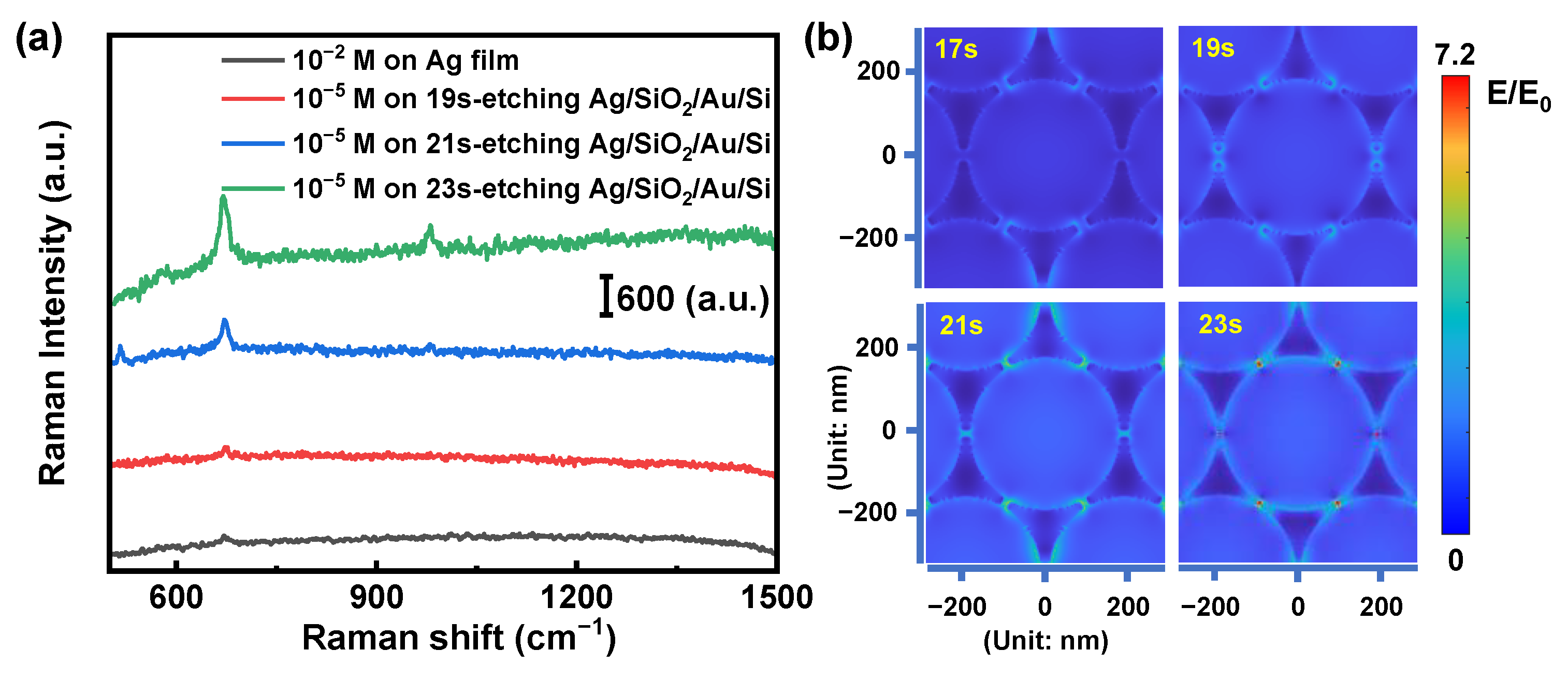
To further confirm that the coupling came into being during the etching process, Raman spectra measurement for melamine was carried out to see the relationship between the degree of etching and the intensity of the Raman signal. Figure 5a shows the SERS signal of 10−5 M melamine on Ag/SiO2/Au/Si structures with different etching times from 19 s to 23 s, respectively. We can see that for the same melamine concentration, the SERS signal increases with the increase in etching time. The Ag/SiO2/Au/Si structures with the 23 s etching time demonstrate the highest Raman intensity. As a control experiment, the Raman signal of melamine was also collected for the bare Ag film. From the experimental results, we can confirm that the SERS performance is highly related to the structural geometry in addition to the Ag itself. To further clarify the change of the coupling between the dips of triangles during etching, the electric field distributions of the nanostructure with different etching times are shown in Figure 5b. In our simulation, the excitation laser wavelength is 532 nm, and the gap distances are retrieved from Figure 4a. Figure 5b clears shows that with the etching time increasing from 19 s to 23 s, the plasmonic coupling between gaps of the triangles gets stronger. Both the experimental and simulated results confirm that the plasmonic resonances and couplings of the metasurfaces play a key role in the SERS signal enhancement.
As known, GO can help adsorb much more targeted molecules and hence chemically enhance the SERS activity [64,65,66]. Therefore, GO-coated plasmonic SERS substrates could have much higher sensitivity and lower detection limits due to a combination of chemical enhancement of GO and the number of hot spots of plasmonic nanostructures. Various methods have been proposed to form thin GO films on structures, such as dip coating, spin coating, and electric-field-assisted coating [67,68,69,70]. For electric-field-assisted coating, the Ag oxidation could be accelerated with the exposure to plasma or chemical solution with electric charges. Both spin coating and dip coating are facile, efficient approaches. However, spin coating is a favorite to achieve the large-area, uniform GO films.
We, therefore, further investigated the SERS performance of the GO-coated MIM substrate. In the Raman spectrum of melamine under excitation of 532 nm laser, there are two major peaks located at 671 cm−1 and 981 cm−1, as shown in Figure 6a, which correspond to the ring breathing vibration and the CNC + NCN bending vibration, respectively [71]. For the peak at 671 cm−1, the corresponding wavelength of the excited Raman signals is 552 nm, which is very close to the coupled resonance wavelength of 555 nm from the Ag/SiO2/Au/Si substrate with the etching time of 23 s. Therefore, we can enhance the Raman signals via both the Purcell effect [51,72,73,74] and the increased absorption efficiency of the excitation light. Figure 6b shows the SEM image of the GO-coated MIM substrate. The inset in Figure 6b illustrates the measured Raman spectrum with two clearly observed peaks at 1356 cm−1 and 1601 cm−1, corresponding to the D and G bands of GO, respectively [65]. Figure 6a shows the SERS signal of 10−6 M melamine on the GO/Ag/SiO2/Au substrate, the Ag/SiO2/Au substrate, and the Raman signal of 10−2 M melamine on the Si substrate, respectively. We can see that with the GO-coating, the Raman signals can be greatly enhanced. The analytical enhancement factor (AEF) [70] is calculated using the equation below to further quantify the enhanced distribution of the SERS substrate:
where ISERS and IREF represent the peak intensity of the Raman signal from the GO/Ag/SiO2/Au/Si substrate and the Raman signal obtained from the Si substrate, respectively. CSERS and CREF are the concentrations of melamine solutions dropped on the SERS and reference substrates, respectively. The peak at 671 cm−1 is chosen to calculate the AEF.
AEF = (ISERS × CREF)/(IREF × CSERS)
Herein, the measured ISERS and CSERS are 2450 and 10−6 M for melamine on the SERS substrate, and the measured IREF and CREF are 227 and 10−2 M for the reference substrate. Thus, the calculated AEF is 1.1 × 10⁵, indicating a high level of SERS performance of the GO-coated MIM substrate. We explored the sensitivity of the optimal SERS substrates further. Figure 6c shows the measured SERS spectra with different melamine concentrations. We can achieve the limit of detection (LOD) as low as 8 × 10⁻⁹ M for the melamine. Figure 6d shows the intensity of the typical Raman peak at 671 cm−1 as a function of melamine concentration on a log scale, demonstrating excellent linear dependency with a correlation coefficient (R2) of 0.978.
For SERS-based molecular detection, in addition to the high sensitivity, uniformity is another important factor for practical applications. We carried out a 10 × 10 µm2 Raman mapping for uniformity evaluation of the modified SERS substrate surface. Figure 7a,b shows the Raman mapping result and the measured SERS spectra of melamine at 16 random positions within the Raman mapping area. It is obvious that the obtained profiles of spectra are almost identical, with neither a significant shift of the characteristic Raman peaks nor the obvious change of the peak intensity, indicating excellent uniformity of the fabricated SERS substrate.
4. Conclusions
In summary, we have demonstrated a facile, cost-effective strategy to achieve highly sensitive and reproducible SERS substrates using a modified NSL technique. Through precise control of nanosphere etching time, we can tune the MIM structure’s absorption to match the excitation laser wavelength as much as possible so as to enhance the light-MIM structure interactions. More importantly, we can precisely control the gap of the Ag nanotriangles to strong plasmonic couplings to further enhance the Raman signals. We have achieved a high-performance SERS activity for melamine with the AEF of 1.1×10⁵ and LOD of 10−9 M within a large area under the 532 nm laser excitation. Our proposed strategy could enable highly sensitive and reproducible SERS substrates with a simple, low-cost, and large-area fabrication process, hence providing a promising platform for SERS-based rapid trace detection in food safety control and environmental monitoring.
Author Contributions
Conceptualization, Z.W., J.L. and Y.J.L.; methodology, Z.W., J.W. and J.L.; software, Z.W. and D.K.; validation, J.L., Z.M., J.W. and Y.J.L.; formal analysis, Z.W.; investigation, Z.W. and J.L.; resources, Z.W., Z.M. and D.K.; data curation, Z.W.; discussion and advising, S.J., D.L., J.L. and Y.J.L.; writing—original draft preparation, Z.W.; writing—review and editing, all authors; visualization, J.L. and Y.J.L.; supervision, Y.J.L.; project administration, Y.J.L.; funding acquisition, Y.J.L. All authors have read and agreed to the published version of the manuscript.
Funding
This work was supported in part by the National Natural Science Foundation of China (Grant No. 62075093), Natural Science Foundation of Guangdong Province (Grant No. 2019A1515110864), Guangdong Innovative and Entrepreneurial Research Team Program (Grant No. 2017ZT07C071), and Shenzhen Science and Technology Innovation Commission (Grant No. GJHZ20180928155207206).
Institutional Review Board Statement
Not applicable.
Informed Consent Statement
Not applicable.
Data Availability Statement
The data presented in this study are available on request from the corresponding author.
Acknowledgments
The authors acknowledge the assistance of SUSTech Core Research Facilities.
Conflicts of Interest
The authors declare no conflict of interest.
References
- Ding, S.-Y.; Yi, J.; Li, J.-F.; Ren, B.; Wu, D.Y.; Panneerselvam, R.; Tian, Z.Q. Nanostructure-based plasmon-enhanced Raman spectroscopy for surface analysis of materials. Nat. Rev. Mater. 2016, 1, 16021. [Google Scholar] [CrossRef]
- Laing, S.; Jamieson, L.E.; Faulds, K.; Graham, D. Surface-enhanced Raman spectroscopy for in vivo biosensing. Nat. Rev. Chem. 2017, 1, 0060. [Google Scholar] [CrossRef]
- Wang, X.; Huang, S.-C.; Hu, S.; Yan, S.; Ren, B. Fundamental understanding and applications of plasmon-enhanced Raman spectroscopy. Nat. Rev. Phys. 2020, 2, 253–271. [Google Scholar] [CrossRef]
- Yin, Z.; Xu, K.; Jiang, S.; Luo, D.; Chen, R.; Xu, C.; Shum, P.; Liu, Y.J. Recent progress on two-dimensional layered materials for surface enhanced Raman spectroscopy and their applications. Mater. Today Phys. 2021, 18, 100378. [Google Scholar] [CrossRef]
- Su, Q.; Ma, X.; Dong, J.; Jiang, C.; Qian, W. A reproducible SERS substrate based on electrostatically assisted APTES-functionalized surface-assembly of gold nanostars. ACS Appl. Mater. Interfaces 2011, 3, 1873–1879. [Google Scholar] [CrossRef]
- He, Y.; Su, S.; Xu, T.; Zhong, Y.; Zapienb, J.A.; Li, J.; Fan, C.; Lee, S.-T. Silicon nanowires-based highly-efficient SERS-active platform for ultrasensitive DNA detection. Nano Today 2011, 6, 122–130. [Google Scholar] [CrossRef]
- Hu, L.; Liu, Y.J.; Xu, S.; Li, Z.; Guo, J.; Gao, S.; Lu, Z.; Si, H.; Jiang, S.; Wang, S. Facile and low-cost fabrication of Ag-Cu substrates via replacement reaction for highly sensitive SERS applications. Chem. Phys. Lett. 2017, 667, 351–356. [Google Scholar] [CrossRef]
- Zhang, C.; Li, C.; Yu, J.; Jiang, S.; Xu, S.; Yang, C.; Liu, Y.J.; Gao, X.; Liu, A.; Man, B. SERS activated platform with three-dimensional hot spots and tunable nanometer gap. Sens. Actuators B Chem. 2018, 258, 163–171. [Google Scholar] [CrossRef]
- Sevim, S.; Franco, C.; Chen, X.-Z.; Sorrenti, A.; Rodríguez-San-Miguel, D.; Pané, S.; deMello, A.J.; Puigmartí-Luis, J. SERS barcode libraries: A microfluidic approach. Adv. Sci. 2020, 7, 1903172. [Google Scholar] [CrossRef] [Green Version]
- Wu, R.; Jin, Q.; Storey, C.; Collins, J.; Gomard, G.; Lemmer, U.; Canham, L.; Kling, R.; Kaplan, A. Gold nanoplasmonic particles in tunable porous silicon 3D scaffolds for ultra-low concentration detection by SERS. Nanoscale Horiz. 2021, 6, 781–790. [Google Scholar] [CrossRef]
- Li, Z.; Leustean, L.; Inci, F.; Zheng, M.; Demirci, U.; Wang, S. Plasmonic-based platforms for diagnosis of infectious diseases at the point-of-care. Biotechnol. Adv. 2019, 37, 107440. [Google Scholar] [CrossRef] [PubMed]
- Xu, K.; Zhou, R.; Takei, K.; Hong, M. Toward flexible surface-enhanced Raman scattering (SERS) sensors for point-of-care diagnostics. Adv. Sci. 2019, 6, 1900925. [Google Scholar] [CrossRef] [PubMed]
- Wang, H.N.; Dhawan, A.; Du, Y.; Batchelor, D.; Leonard, D.N.; Misra, V.; Vo-Dinh, T. Molecular sentinel-on-chip for SERS-based biosensing. Phys. Chem. Chem. Phys. 2013, 15, 6008–6015. [Google Scholar] [CrossRef] [PubMed] [Green Version]
- Wang, P.-L.; Xie, L.-H.; Joseph, E.A.; Li, J.-R.; Su, X.-O.; Zhou, H.-C. Metal–organic frameworks for food safety. Chem. Rev. 2019, 119, 10638–10690. [Google Scholar] [CrossRef] [PubMed]
- Langer, J.; de Aberasturi, D.J.; Aizpurua, J.; Alvarez-Puebla, R.A.; Auguié, B.; Baumberg, J.J.; Bazan, G.C.; Bell, S.E.J.; Boisen, A.; Brolo, A.G.; et al. Present and future of surface-enhanced Raman scattering. ACS Nano 2020, 14, 28–117. [Google Scholar] [CrossRef] [Green Version]
- Zhou, X.; Hu, Z.; Yang, D.; Xie, S.; Jiang, Z.; Niessner, R.; Haisch, C.; Zhou, H.; Sun, P. Bacteria detection: From powerful SERS to its advanced compatible techniques. Adv. Sci. 2020, 7, 2001739. [Google Scholar] [CrossRef]
- Moore, T.J.; Moody, A.S.; Payne, T.D.; Sarabia, G.M.; Daniel, A.R.; Sharma, B. In vitro and in vivo SERS biosensing for disease diagnosis. Biosensors 2018, 8, 46. [Google Scholar] [CrossRef] [Green Version]
- Zong, C.; Xu, M.; Xu, L.-J.; Wei, T.; Ma, X.; Zheng, X.-S.; Hu, R.; Ren, B. Surface-enhanced Raman spectroscopy for bioanalysis: Reliability and challenges. Chem. Rev. 2018, 118, 4946–4980. [Google Scholar] [CrossRef]
- Zhao, X.; Liu, C.; Yu, J.; Li, Z.; Liu, L.; Li, C.; Xu, S.; Li, W.; Man, B.; Zhang, C. Hydrophobic multiscale cavities for high-performance and self-cleaning surface-enhanced Raman spectroscopy (SERS) sensing. Nanophotonics 2020, 9, 4761–4773. [Google Scholar] [CrossRef]
- Li, W.; Zamani, R.; Gil, P.R.; Pelaz, B.; Ibáñez, M.; Cadavid, D.; Shavel, A.; Alvarez-Puebla, R.A.; Parak, W.J.; Arbiol, J.; et al. CuTe nanocrystals: Shape and size control, plasmonic properties, and use as SERS probes and photothermal agents. J. Am. Chem. Soc. 2013, 135, 7098–7101. [Google Scholar] [CrossRef]
- Cong, S.; Yuan, Y.; Chen, Z.; Hou, J.; Yang, M.; Su, Y.; Zhang, Y.; Li, L.; Li, Q.; Geng, F.; et al. Noble metal-comparable SERS enhancement from semiconducting metal oxides by making oxygen vacancies. Nat. Commun. 2015, 6, 7800. [Google Scholar] [CrossRef] [PubMed]
- Yao, Y.; Liao, Z.; Liu, Z.; Liu, X.; Zhou, J.; Liu, G.; Yi, Z.; Wang, J. Recent progresses on metamaterials for optical absorption and sensing: A review. J. Phys. D Appl. Phys. 2021, 54, 113002. [Google Scholar] [CrossRef]
- Ding, S.-Y.; You, E.-M.; Tian, Z.-Q.; Moskovits, M. Electromagnetic theories of surface-enhanced Raman spectroscopy. Chem. Soc. Rev. 2017, 46, 4042–4076. [Google Scholar] [CrossRef] [PubMed]
- Albella, P.; de la Osa, R.A.; Moreno, F.; Maier, S.A. Electric and magnetic field enhancement with ultralow heat radiation dielectric nanoantennas: Considerations for surface-enhanced spectroscopies. ACS Photonics 2014, 1, 524–529. [Google Scholar] [CrossRef]
- Szlag, V.M.; Rodriguez, R.S.; He, J.; Hudson-Smith, N.; Kang, H.; Le, N.; Reineke, T.M.; Haynes, C.L. Molecular affinity agents for intrinsic surface-enhanced Raman scattering (SERS) sensors. ACS Appl. Mater. Interfaces 2018, 10, 31825–31844. [Google Scholar] [CrossRef]
- Huang, J.; Zhang, L.; Chen, B.; Ji, N.; Chen, F.; Zhang, Y.; Zhang, Z. Nanocomposites of size-controlled gold nanoparticles and graphene oxide: Formation and applications in SERS and catalysis. Nanoscale 2010, 2, 2733–2738. [Google Scholar] [CrossRef]
- Giner-Casaresa, J.J.; Liz-Marzána, L.M. Plasmonic nanoparticles in 2D for biological applications: Toward active multipurpose platforms. Nano Today 2014, 9, 365–377. [Google Scholar] [CrossRef]
- Wei, H.; Xu, H. Hot spots in different metal nanostructures for plasmon-enhanced Raman spectroscopy. Nanoscale 2013, 5, 10794–10805. [Google Scholar] [CrossRef]
- Kasani, S.; Curtin, K.; Wu, N. A review of 2D and 3D plasmonic nanostructure array patterns: Fabrication, light management and sensing applications. Nanophotonics 2019, 8, 2065–2089. [Google Scholar] [CrossRef]
- Jeong, H.-H.; Choi, E.; Ellis, E.; Lee, T.-C. Recent advances in gold nanoparticles for biomedical applications: From hybrid structures to multi-functionality. J. Mater. Chem. B 2019, 7, 3480–3496. [Google Scholar] [CrossRef] [Green Version]
- Gwo, S.; Wang, C.-Y.; Chen, H.-Y.; Lin, M.-H.; Sun, L.; Li, X.; Chen, W.-L.; Chang, Y.-M.; Ahn, H. Plasmonic metasurfaces for nonlinear optics and quantitative SERS. ACS Photonics 2016, 3, 1371–1384. [Google Scholar] [CrossRef]
- Liu, J.X.; He, H.L.; Xiao, D.; Yin, S.T.; Ji, W.; Jiang, S.Z.; Luo, D.; Wang, B.; Liu, Y.J. Recent advances of plasmonic nanoparticles and their applications. Materials 2018, 11, 1833. [Google Scholar] [CrossRef] [PubMed] [Green Version]
- Fan, F.-R.; Lin, L.; Zhu, G.; Wu, W.; Zhang, R.; Wang, Z.L. Transparent triboelectric nanogenerators and self-powered pressure sensors based on micropatterned plastic films. Nano Lett. 2012, 12, 3109–3114. [Google Scholar] [CrossRef] [PubMed] [Green Version]
- Hatab, N.A.; Hsueh, C.-H.; Gaddis, A.L.; Retterer, S.T.; Li, J.-H.; Eres, G.; Zhang, Z.; Gu, B. Free-standing optical gold bowtie nanoantenna with variable gap size for enhanced Raman spectroscopy. Nano Lett. 2010, 10, 4952–4955. [Google Scholar] [CrossRef]
- Pan, R.; Yang, Y.; Wang, Y.; Li, S.; Liu, Z.; Su, Y.; Quan, B.; Li, Y.; Gu, C.; Li, J. Nanocracking and metallization doubly defined large-scale 3D plasmonic sub-10 nm-gap arrays as extremely sensitive SERS substrates. Nanoscale 2018, 10, 3171–3180. [Google Scholar] [CrossRef] [Green Version]
- Zhu, C.; Meng, G.; Zheng, P.; Huang, Q.; Li, Z.; Hu, X.; Wang, X.; Huang, Z.; Li, F.; Wu, N. A hierarchically ordered array of silver-nanorod bundles for surface-enhanced Raman scattering detection of phenolic pollutants. Adv. Mater. 2016, 28, 4871–4876. [Google Scholar] [CrossRef]
- Yang, F.; Zhang, H.; Feng, H.; Dong, J.; Wang, C.; Liu, Q. Bionic SERS chip with super-hydrophobic and plasmonic micro/nano dual structure. Photonics Res. 2018, 6, 77–83. [Google Scholar] [CrossRef]
- Feng, H.; Dong, J.; Wu, X.; Yang, F.; Ma, L.; Liu, X.; Liu, Q. Ultra-large local field enhancement effect of isolated thick triangular silver nanoplates on a silicon substrate in the green waveband. Opt. Lett. 2020, 45, 2099–2102. [Google Scholar] [CrossRef]
- Cui, L.; Wang, A.; Wu, D.-Y.; Ren, B.; Tian, Z.-Q. Shaping and shelling Pt and Pd nanoparticles for ultraviolet laser excited surface-enhanced Raman scattering. J. Phys. Chem. C 2008, 112, 17618–17624. [Google Scholar] [CrossRef]
- Cui, L.; Mahajan, S.; Cole, R.M.; Soares, B.; Bartlett, P.N.; Baumberg, J.J.; Hayward, I.P.; Ren, B.; Russell, A.E.; Tian, Z.Q. UV SERS at well ordered Pd sphere segment void (SSV) nanostructures. Phys. Chem. Chem. Phys. 2009, 11, 1023–1026. [Google Scholar] [CrossRef] [Green Version]
- Jha, S.K.; Ahmed, Z.; Agio, M.; Ekinci, Y.; Löffler, J.F. Deep-UV surface-enhanced resonance Raman scattering of adenine on aluminum nanoparticle arrays. J. Am. Chem. Soc. 2012, 134, 1966–1969. [Google Scholar] [CrossRef] [PubMed]
- Kämmer, E.; Dörfer, T.; Csáki, A.; Schumacher, W.; Da Costa Filho, P.A.; Tarcea, N.; Fritzsche, W.; Rösch, P.; Schmitt, M.; Popp, J. Evaluation of colloids and activation agents for determination of melamine using UV-SERS. J. Phys. Chem. C 2012, 116, 6083–6091. [Google Scholar] [CrossRef] [PubMed]
- Li, Z.-Y. Mesoscopic and microscopic strategies for engineering plasmon-enhanced Raman scattering. Adv. Opt. Mater. 2018, 6, 1701097. [Google Scholar] [CrossRef]
- Dong, N.; Hu, Y.; Yang, K.; Liu, J. Development of aptamer-modified SERS nanosensor and oligonucleotide chip to quantitatively detect melamine in milk with high sensitivity. Sens. Actuators B 2016, 228, 85–93. [Google Scholar] [CrossRef]
- Li, R.; Yang, J.; Han, J.; Liu, J.; Huang, M. Quantitative determination of melamine in milk using Ag nanoparticle monolayer film as SERS substrate. Phys. E 2017, 88, 164–168. [Google Scholar] [CrossRef]
- Huang, J.; Chen, F.; Zhang, Q.; Zhan, Y.; Ma, D.; Xu, K.; Zhao, Y. 3D silver nanoparticles decorated zinc oxide/silicon heterostructured nanomace arrays as high performance surface-enhanced Raman scattering substrates. ACS Appl. Mater. Interfaces 2015, 7, 5725–5735. [Google Scholar] [CrossRef] [PubMed]
- Sivashanmugan, K.; Liao, J.-D.; Liu, B.H.; Yu, L.C. AuGa2 on focused Ga ion beam fabricated Au nanorod array for trace detection of melamine cyanurate in milk solution. Appl. Phys. Exp. 2015, 8, 017001. [Google Scholar] [CrossRef]
- Cossio, G.; Yu, E.T. Zeta potential dependent self-assembly for very large area nanosphere lithography. Nano Lett. 2020, 20, 5090–5096. [Google Scholar] [CrossRef]
- Dai, Z.; Mei, F.; Xiao, X.; Liao, L.; Fu, L.; Wang, J.; Wu, W.; Guo, S.; Zhao, X.; Li, W.; et al. “Rings of saturn-like” nanoarrays with high number density of hot spots for surface-enhanced Raman scattering. Appl. Phys. Lett. 2014, 105, 033515. [Google Scholar] [CrossRef]
- Fang, X.; Zheng, C.; Yin, Z.; Wang, Z.; Wang, J.; Liu, J.; Luo, D.; Liu, Y.J. Hierarchically ordered silicon metastructures from improved self-assembly-based nanosphere lithography. ACS Appl. Mater. Interfaces 2020, 12, 12345–12352. [Google Scholar] [CrossRef]
- Wang, Z.; Liu, J.; Fang, X.; Wang, J.; Yin, Z.; He, H.; Jiang, S.; Zhao, M.; Yin, Z.; Luo, D.; et al. Plasmonically enhanced photoluminescence of monolayer MoS2 via nanosphere lithography templated gold metasurfaces. Nanophotonics 2021, 10, 1733–1740. [Google Scholar] [CrossRef]
- Hulteen, J.C.; Treichel, D.A.; Smith, M.T.; Duval, M.L.; Jensen, T.R.; Van Duyne, R.P. Nanosphere lithography: Size-tunable silver nanoparticle and surface cluster arrays. J. Phys. Chem. B 1999, 103, 3854–3863. [Google Scholar] [CrossRef]
- Wang, T.-J.; Hsu, K.-C.; Liu, Y.-C.; Lai, C.-H.; Chiang, H.-P. Nanostructured SERS substrates produced by nanosphere lithography and plastic deformation through direct peel-off on soft matter. J. Opt. 2016, 18, 055006. [Google Scholar] [CrossRef]
- Wuytens, P.C.; Skirtach, A.G.; Baets, R. On-chip surface-enhanced Raman spectroscopy using nanosphere-lithography patterned antennas on silicon nitride waveguides. Opt. Express 2017, 25, 12926–12934. [Google Scholar] [CrossRef] [PubMed] [Green Version]
- Chau, Y.-F.C.; Chen, K.-H.; Chiang, H.-P.; Lim, C.M.; Huang, H.J.; Lai, C.-H.; Kumara, N.T.R.N. Fabrication and characterization of a metallic-dielectric nanorod array by nanosphere lithography for plasmonic sensing application. Nanomaterials 2019, 9, 1691. [Google Scholar] [CrossRef] [Green Version]
- Zhang, W.; Xue, T.; Zhang, L.; Lu, F.; Liu, M.; Meng, C.; Mao, D.; Mei, T. Surface-enhanced Raman spectroscopy based on a silver-film semi-coated nanosphere array. Sensors 2019, 19, 3966. [Google Scholar] [CrossRef] [PubMed] [Green Version]
- Zhang, L.; Meng, C.; Zhang, G.; Bai, D.; Gao, F.; Xu, L.; Zhang, W.; Mei, T.; Zhao, J. Nanofocusing of a metallized double periodic arranged nanocone array for surface-enhanced Raman spectroscopy. Opt. Express 2021, 29, 28086–28095. [Google Scholar] [CrossRef]
- Jeon, T.Y.; Kim, D.J.; Park, S.-G.; Kim, S.-H.; Kim, D.-H. Nanostructured plasmonic substrates for use as SERS sensors. Nano Converg. 2016, 3, 18. [Google Scholar] [CrossRef] [Green Version]
- Xia, L.; Yang, Z.; Yin, S.; Guo, W.; Li, S.; Xie, W.; Huang, D.; Deng, Q.; Shi, H.; Cui, H.; et al. Surface enhanced Raman scattering substrate with metallic nanogap array fabricated by etching the assembled polystyrene spheres array. Opt. Express 2013, 21, 11349–11355. [Google Scholar] [CrossRef]
- Cai, H.; Wu, Y.; Dai, Y.; Pan, N.; Tian, Y.; Luo, Y.; Wang, X. Wafer scale fabrication of highly dense and uniform array of sub-5 nm nanogaps for surface enhanced Raman scatting substrates. Opt. Express 2016, 24, 20808–20815. [Google Scholar] [CrossRef]
- Wang, H.; Rao, G.; Wang, Y.; Du, X.; Zhang, M.; Wang, X.; Hu, A.; Hu, Y.; Huang, J.; Chu, J.; et al. Low field gradient and highly enhanced plasmonic nanocavity array for supersensitive determination of multiple hazardous chemical residues. J. Phys. Chem. C 2021, 125, 4710–4719. [Google Scholar] [CrossRef]
- Men, D.; Liu, G.; Xing, C.; Zhang, H.; Xiang, J.; Sun, Y.; Hang, L. Dynamically tunable plasmonic band for reversible colorimetric sensors and surface-enhanced Raman scattering effect with good sensitivity and stability. ACS Appl. Mater. Interfaces 2020, 12, 7494–7503. [Google Scholar] [CrossRef] [PubMed]
- Merk, V.; Kneipp, J.; Leosson, K. Gap size reduction and increased SERS enhancement in lithographically patterned nanoparticle arrays by templated growth. Adv. Opt. Mater. 2013, 1, 313–318. [Google Scholar] [CrossRef]
- Lee, J.; Kim, J.; Kim, S.; Min, D.-H. Biosensors based on graphene oxide and its biomedical application. Adv. Drug Deliv. Rev. 2016, 105, 275–287. [Google Scholar] [CrossRef]
- Hu, L.; Liu, Y.J.; Han, Y.; Chen, P.; Zhang, C.; Li, C.; Lu, Z.; Luo, D.; Jiang, S. Graphene oxide-decorated silver dendrites for high-performance surface-enhanced Raman scattering applications. J. Mater. Chem. C 2017, 5, 3908–3915. [Google Scholar] [CrossRef]
- Lu, Z.; Liu, Y.; Wang, M.; Zhang, C.; Li, Z.; Huo, Y.; Li, Z.; Xu, S.; Man, B.; Jiang, S. A novel natural surface-enhanced Raman spectroscopy (SERS) substrate based on graphene oxide-Ag nanoparticles-Mytilus coruscus hybrid system. Sens. Actuators B Chem. 2018, 261, 1–10. [Google Scholar] [CrossRef]
- Grazia, G.P.; Carlo, V.; Giovanni, D.; Carlo, V. Spectroscopic ellipsometry investigation of the optical properties of graphene oxide dip-coated on magnetron sputtered gold thin films. J. Appl. Phys. 2018, 123, 055303. [Google Scholar]
- Li, Z.; Jiang, S.; Huo, Y.; Ning, T.; Liu, A.; Zhang, C.; He, Y.; Wang, M.; Li, C.; Man, B. 3D silver nanoparticles with multilayer graphene oxide as a spacer for surface enhanced Raman spectroscopy analysis. Nanoscale 2018, 10, 5897. [Google Scholar] [CrossRef]
- Zhang, L.; Jiang, C.; Zhang, Z. Graphene oxide embedded sandwich nanostructures for enhanced Raman readout and their applications in pesticide monitoring. Nanoscale 2013, 5, 3773. [Google Scholar] [CrossRef]
- Yin, Z.; He, H.; Wang, Z.; Fang, X.; Xu, C.; Luo, D.; Jiang, S.; Liu, Y.J. Facile in situ photochemical synthesis of silver nanoaggregates for surface-enhanced Raman scattering applications. Nanomaterials 2020, 10, 685. [Google Scholar] [CrossRef] [Green Version]
- Mircescu, N.E.; Oltean, M.; Chis, V.; Leopold, N. FTIR, FT-Raman, SERS and DFT study on melamine. Vib. Spectrosc. 2012, 62, 165–171. [Google Scholar] [CrossRef]
- Sun, G.; Khurgin, J.B.; Soref, R.A. Plasmonic light-emission enhancement with isolated metal nanoparticles and their coupled arrays. J. Opt. Soc. Am. B 2008, 25, 1748–1755. [Google Scholar] [CrossRef]
- Mak, K.F.; Shan, J. Photonics and optoelectronics of 2D semiconductor transition metal dichalcogenides. Nat. Photonics 2016, 10, 216–226. [Google Scholar] [CrossRef]
- Park, K.-D.; Jiang, T.; Clark, G.; Xu, X.; Raschke, M.B. Radiative control of dark excitons at room temperature by nano-optical antenna-tip Purcell effect. Nat. Nanotechnol. 2018, 13, 59–64. [Google Scholar] [CrossRef] [Green Version]
Figure 1.
Schematic illustration of trace melamine measurement using the GO/Ag/SiO2/Au/Si SERS substrate. The gray spheres represent the melamine molecules. The right top illustrates the molecular structure of melamine.
Figure 1.
Schematic illustration of trace melamine measurement using the GO/Ag/SiO2/Au/Si SERS substrate. The gray spheres represent the melamine molecules. The right top illustrates the molecular structure of melamine.

Figure 2.
(a) Schematic fabrication processes for the Ag metasurfaces without ICP etching. (b) Measured reflection spectra with different insulator gaps.
Figure 2.
(a) Schematic fabrication processes for the Ag metasurfaces without ICP etching. (b) Measured reflection spectra with different insulator gaps.

Figure 3.
(a) Schematic fabrication processes for the Ag metasurfaces with ICP etching. Typical SEM images of the templated masks are comparatively illustrated before and after ICP etching. (b–g) SEM images of the fabricated Ag metasurfaces without and with ICP etching, respectively.
Figure 3.
(a) Schematic fabrication processes for the Ag metasurfaces with ICP etching. Typical SEM images of the templated masks are comparatively illustrated before and after ICP etching. (b–g) SEM images of the fabricated Ag metasurfaces without and with ICP etching, respectively.

Figure 4.
(a) Measured the gap distances between the adjacent nanotriangles at different etching times. (b,c) Simulated and measured reflection spectra of the MIM substrate with different gaps. (d) Measured absorbance spectra of the MIM substrate with different gaps.
Figure 4.
(a) Measured the gap distances between the adjacent nanotriangles at different etching times. (b,c) Simulated and measured reflection spectra of the MIM substrate with different gaps. (d) Measured absorbance spectra of the MIM substrate with different gaps.

Figure 5.
(a) Measured SERS spectra for the 10−5 M melamine on the Ag/SiO2/Au/Si substrates with different etching times of 19 s, 21 s, 23 s, and 10−2 M melamine on the Ag film substrate, respectively. (b) Electric field distributions on the nanostructured surface with different etching times. Scale bar: 100 nm.

Figure 6.
(a) Measured SERS spectra with 10−6 M melamine on the GO/Ag/SiO2/Au/Si substrate, the Ag/SiO2/Au substrate, and 10−2 M melamine on the Si substrate, respectively. (b) SEM image of GO-coated Ag metasurface. The inset shows the Raman spectrum of GO on the metasurface. (c) Measured SERS spectra for melamine with different concentrations from 1 × 10⁻⁵ M to 8 × 10⁻⁹ M on the GO/Ag/SiO2/Au/Si substrate. The inset illustrates the Raman peak of trace melamine with a concentration of 8 × 10⁻⁹ M at 671 cm−1. (d) Raman intensity of melamine at 671 cm−1 as a function of different concentrations in log scale.

Figure 7.
(a) Raman mapping of 10−5 M melamine with the collected signal of peak A at 671 cm−1. (b) Collected Raman signals of 10−5 M melamine at 16 randomly selected positions within the Raman mapping area.
Figure 7.
(a) Raman mapping of 10−5 M melamine with the collected signal of peak A at 671 cm−1. (b) Collected Raman signals of 10−5 M melamine at 16 randomly selected positions within the Raman mapping area.

Publisher’s Note: MDPI stays neutral with regard to jurisdictional claims in published maps and institutional affiliations. |
© 2022 by the authors. Licensee MDPI, Basel, Switzerland. This article is an open access article distributed under the terms and conditions of the Creative Commons Attribution (CC BY) license (https://creativecommons.org/licenses/by/4.0/).
Share and Cite
MDPI and ACS Style
Wang, Z.; Liu, J.; Wang, J.; Ma, Z.; Kong, D.; Jiang, S.; Luo, D.; Liu, Y.J. Graphene Oxide-Coated Metal–Insulator–Metal SERS Substrates for Trace Melamine Detection. Nanomaterials 2022, 12, 1202. https://doi.org/10.3390/nano12071202
AMA Style
Wang Z, Liu J, Wang J, Ma Z, Kong D, Jiang S, Luo D, Liu YJ. Graphene Oxide-Coated Metal–Insulator–Metal SERS Substrates for Trace Melamine Detection. Nanomaterials. 2022; 12(7):1202. https://doi.org/10.3390/nano12071202
Chicago/Turabian StyleWang, Zhenming, Jianxun Liu, Jiawei Wang, Zongjun Ma, Delai Kong, Shouzhen Jiang, Dan Luo, and Yan Jun Liu. 2022. "Graphene Oxide-Coated Metal–Insulator–Metal SERS Substrates for Trace Melamine Detection" Nanomaterials 12, no. 7: 1202. https://doi.org/10.3390/nano12071202
Note that from the first issue of 2016, this journal uses article numbers instead of page numbers. See further details here.