
Structural Engineering Effects on Hump Characteristics of ZnO/InSnO Heterojunction Thin-Film Transistors


1
Institute of Microelectronics, Peking University, Beijing 100871, China
2
School of Information & Communication Engineering, Beijing Information Science and Technology University, Beijing 100101, China
*
Authors to whom correspondence should be addressed.
Nanomaterials 2022, 12(7), 1167; https://doi.org/10.3390/nano12071167
Submission received: 17 February 2022
/
Revised: 27 March 2022
/
Accepted: 28 March 2022
/
Published: 31 March 2022
(This article belongs to the Special Issue Transparent Conductive Nanomaterials: Science and Applications)
Abstract
:Transparent conductive oxides (TCO) have been extensively investigated as channel materials for thin-film transistors (TFTs). In this study, highly transparent and conductive InSnO (ITO) and ZnO films were deposited, and their material properties were studied in detail. Meanwhile, we fabricated ZnO/ITO heterojunction TFTs, and explored the effects of channel structures on the hump characteristics of ZnO/ITO TFTs. We found that Vhump–VON was negatively correlated with the thickness of the bottom ZnO layer (10, 20, 30, and 40 nm), while it was positively correlated with the thickness of the top ITO layer (3, 5, 7, and 9 nm), where Vhump is the gate voltage corresponding to the occurrence of the hump and VON is the turn-on voltage. The results demonstrated that carrier transport forms dual current paths through both the ZnO and ITO layers, synthetically determining the hump characteristics of the ZnO/ITO TFTs. Notably, the hump was effectively eliminated by reducing the ITO thickness to no more than 5 nm. Furthermore, the hump characteristics of the ZnO/ITO TFTs under positive gate-bias stress (PBS) were examined. This work broadens the practical application of TCO and provides a promising method for solving the hump phenomenon of oxide TFTs.
1. Introduction
Oxide thin-film transistors (TFTs) are one of the most important applications of transparent conductive oxides (TCO). Recently, TFTs based on TCO have been extensively investigated for the purpose of achieving transparent and flexible displays [1,2,3,4]. Among the candidates of TCO, InSnO (ITO), and ZnO are considered to be promising channel materials of TFTs since they combine excellent electrical properties and high transmittance [5,6]. Furthermore, heterojunction TFTs, which have bilayer-structure channel, have currently drawn considerable attention. Compared with the conventional oxide TFTs with single-layer channels, the heterojunction TFTs are more flexible in device configuration; thus, they better balance performance with stability [7,8,9]. Therefore, it is necessary to investigate the heterojunction oxide TFTs further.
As a crucial issue to be solved, the hump phenomenon emerging in transfer curves negatively shifts the turn-on voltage (VON) of the oxide TFTs, which not only adversely affects pixel brightness but also increases the power consumption of the displays [10]. The hump phenomenon has been widely examined for the single-channel oxide TFTs [11,12,13,14]. Mechanisms including edge effects, charge trapping, multiple current paths, and creation of donor/acceptor-like defects have been proposed [15,16,17,18,19,20]. Nevertheless, there are relatively few studies on the hump phenomena of heterojunction TFTs. Maeng et al. reported the appearance of humps in heterojunction TFTs as the total channel thickness exceeded 80 nm, and this was explained as being a result of back channel conduction [21]. Zhao et al. demonstrated that the humps in heterojunction TFTs are related to channel thickness and results from large total carrier numbers [22]. Even though these studies involve the hump phenomenon in heterojunction TFTs, the effects of channel structure on hump characteristics have not yet been fully studied. Therefore, further investigation is required to make an in-depth and comprehensive analysis of the influence of channel structure on hump characteristics.
In this work, we examined ZnO/ITO heterojunction TFTs. A systematic study on the characteristics of transparent conductive ITO and ZnO films was conducted, including optical transmittance, carrier concentration, material components, and surface morphology. Furthermore, we determined the effects of the channel structure on the hump characteristics of ZnO/ITO TFTs, and explored the hump characteristics under positive gate-bias stress (PBS).
2. Experimental Methods
2.1. Fabrication of Films and Devices
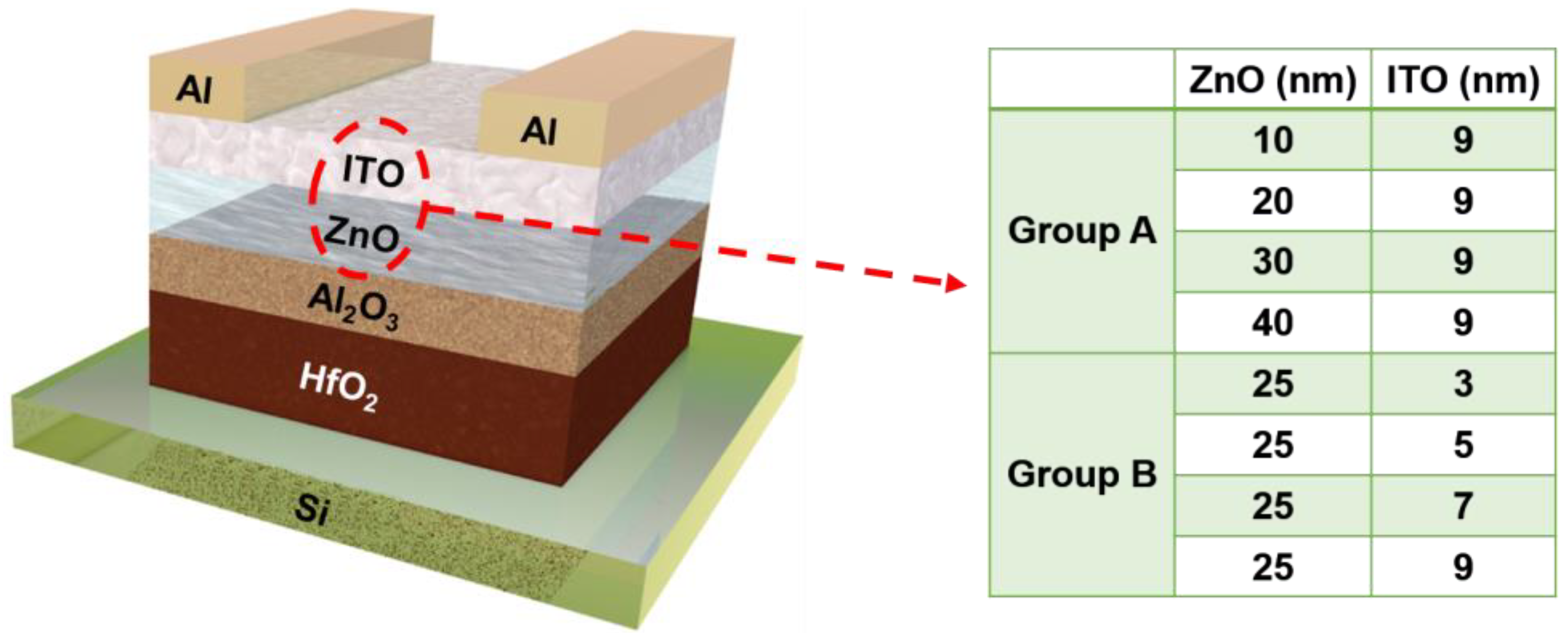
The ZnO and ITO films were deposited on both amorphous glass substrates and single-crystal Si substrates, in which ZnO film was deposited by atomic layer deposition (ALD) at 120 °C and ITO film was sputtered at room temperature. Figure 1 illustrates the device structure of the ZnO/ITO TFTs. A heavy-doped Si wafer was utilized as a substrate and gate electrode. Firstly, 25-nm HfO2 was sputtered at room temperature, and 15-nm Al2O3 was deposited by ALD at 100 °C. Subsequently, the ZnO/ITO heterojunction channel was deposited, where the ZnO layer and ITO layer were deposited using the deposition process mentioned above. Trimethylaluminum (TMA), diethylzinc (DEZ), and deionized water (H2O) were the precursors for the aluminum, zinc, and oxygen elements, respectively. Finally, a 100-nm Al film was sputtered as source/drain electrode. Two experimental groups (A and B) were designed, and corresponding channel structures are also shown in Figure 1.
2.2. Characterization of Films and Devices
Before measurement, the films and devices were subjected to post-annealing treatment at 100 °C in vacuum for 1 h. To obtain the transparency and optical band gap of the ZnO and ITO films, we tested the transmittance (Zolix Omni-λ500, Beijing, China). The carrier concentration and resistivity were determined by Hall measurement (Ecopia HMS-3000, Anyang, South Korea). X-ray photoelectron spectroscopy (XPS, Kratos Axis Ultra, Manchester, United Kingdom) was performed to analyze the chemical composition and elemental states. Furthermore, the surface morphology and microstructure were characterized by atomic force microscope (AFM, Dimension Icon, Bruker, Billerica, MA, USA; Tipsmodel, Scan ASYST-Air) and transmission electron microscope (TEM, FEI Tecnai F20, Hillsboro, OR, USA), respectively. Furthermore, all the electrical characteristic curves of the TFTs were characterized using a semiconductor device analyzer (Agilent B1500A, Palo Alto, CA, USA) under dark ambient conditions at room temperature.
3. Results and Discussion
3.1. Material Properties of ZnO and ITO Films
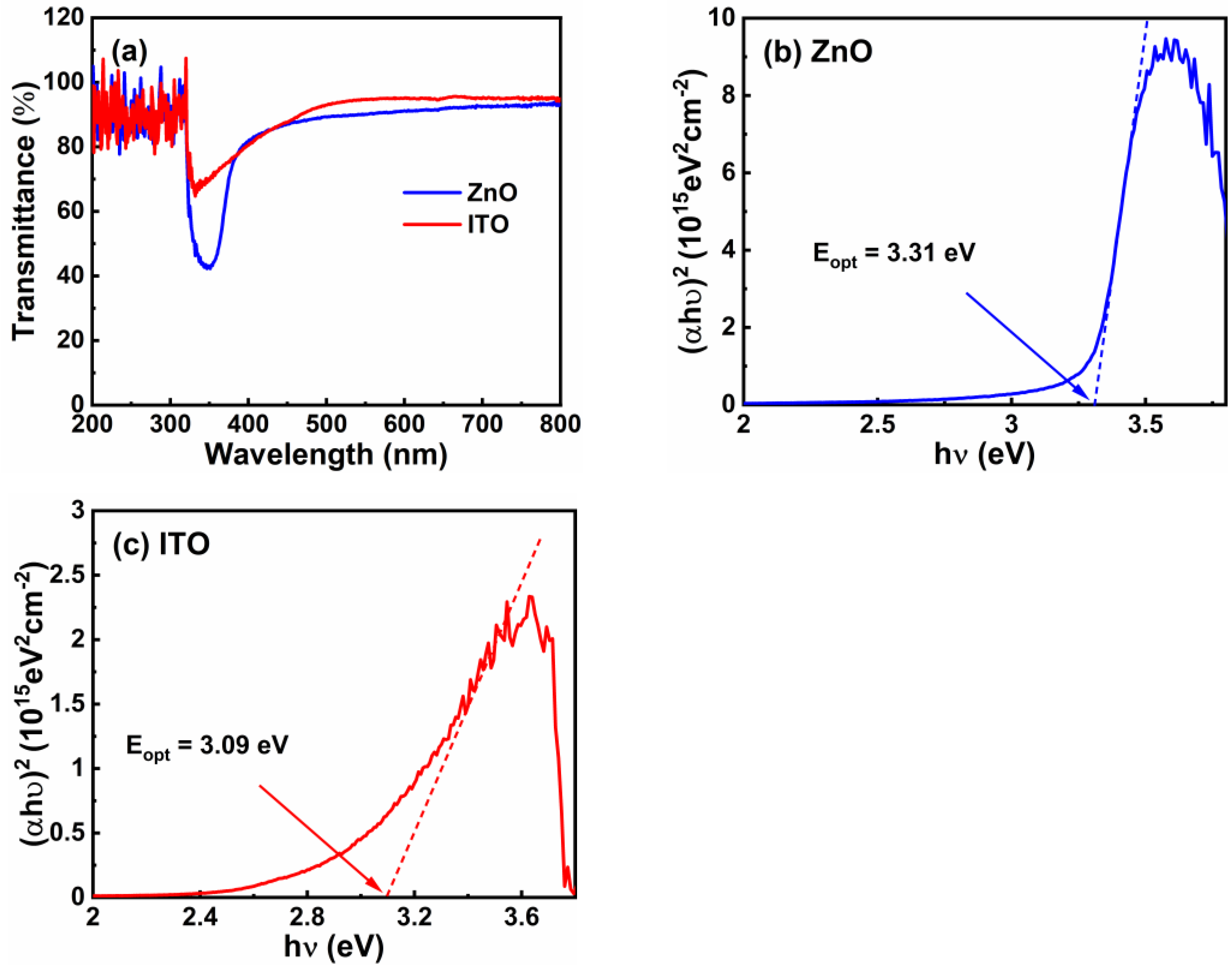
The transmittance spectra of the ZnO and ITO films on glass substrates were characterized, as revealed in Figure 2a. The testing methods were as follows. First, a bare glass substrate was measured as the reference value (Tr). Then, the ZnO and ITO films on the glass substrates were measured as the characteristic value (Tc). Finally, we calculated the transmittance with the characteristic value divided by the reference value (Tr/Tc). Clearly, both the ZnO and ITO films possessed an average optical transparency of over 90% in the visible light range. Furthermore, transmittance of the ITO film was higher than that of the ZnO film. The relationship between the optical energy gap (Eopt) and (αhν)2 of the ZnO and ITO films is shown in Figure 2b,c, respectively. Here, the Eopt of ZnO and ITO films were calculated using the following equations:
where α is the optical absorption coefficient; t is the thickness of the film; T is the average optical transparency; h is the Planck constant; and D is a constant [23]. It is shown that the Eopt value of the ZnO and ITO films is 3.31 and 3.09 eV, respectively.
The carrier concentration and conductivity of the single ITO and ZnO films were determined by Hall measurement, as shown in Table 1. The results showed that the carrier concentration and conductivity of the ITO film were three orders of magnitude higher than those of the ZnO film. Figure 3 shows the XPS O 1 s spectra for the ZnO and ITO films. Firstly, the binding energy (BE) was calibrated by the standard C 1 s line at 284.80 eV [24]. Based on Gaussian fitting, the O 1 s spectra were divided into three individual peaks centered at ~530.1 eV (O1 peak), ~531.1 eV (O2 peak), and ~532.1 eV (O3 peak). The O1 peak represents the metal–oxygen lattice whereas the O2 peak represents oxygen vacancy. The O3 peak, however, is usually related to adsorbed oxygen [25,26]. Here, the area ratios of oxygen vacancy in the ZnO and ITO films were calculated to be 16.68% and 21.04%, respectively. Since the oxygen vacancy can serve as a shallow donor, the variation of oxygen vacancy concentration directly alters the carrier concentration of the film [27]. The intensity ratio of the O2 peak is consistent with the Hall effect results.
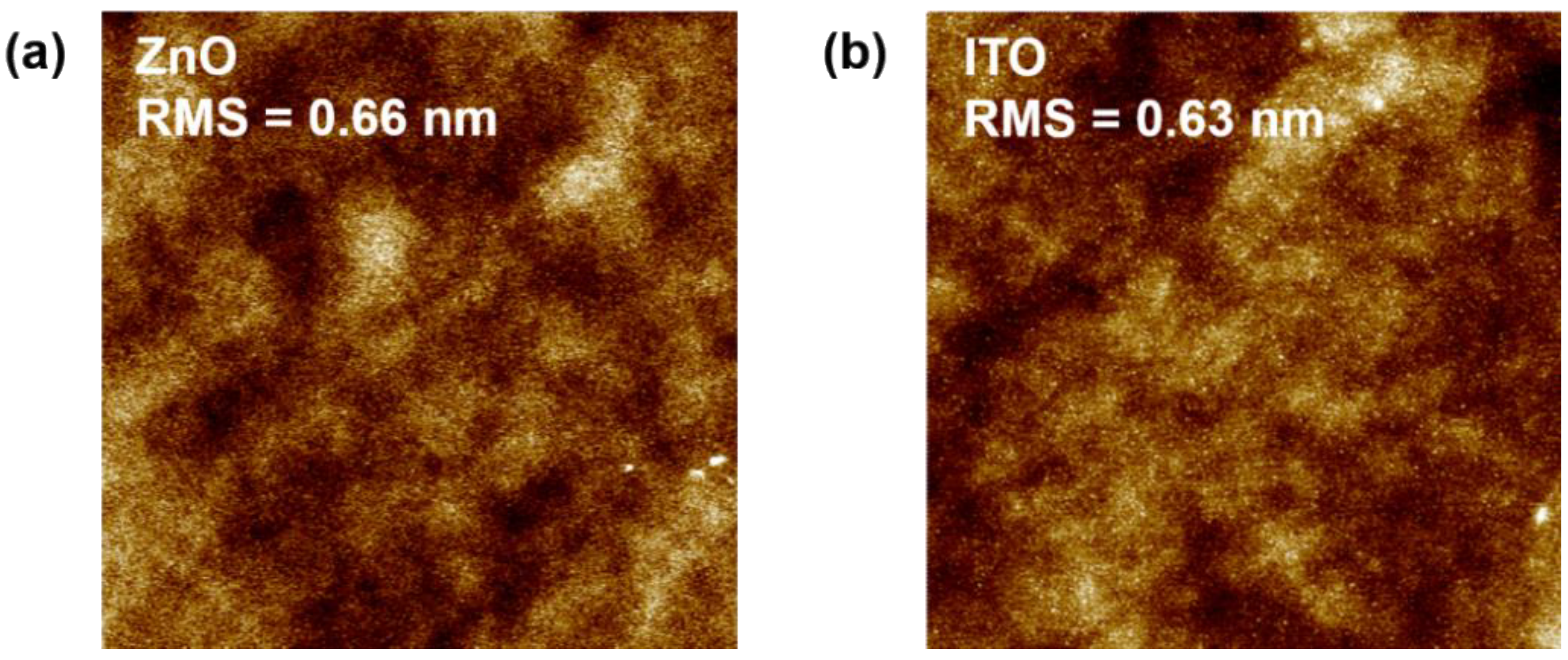
We also examined the surface morphology of the ZnO and ITO films by means of AFM, as shown in Figure 4. The AFM images were measured in a 5 µm × 5 µm area. The root mean square (RMS) roughness of the ZnO and ITO films was 0.66 and 0.63 nm, respectively. A smooth surface is beneficial to reduce the scattering center and optimize the electrical properties of the oxide TFTs [28].
3.2. Hump Characteristics of ZnO/ITO TFTs
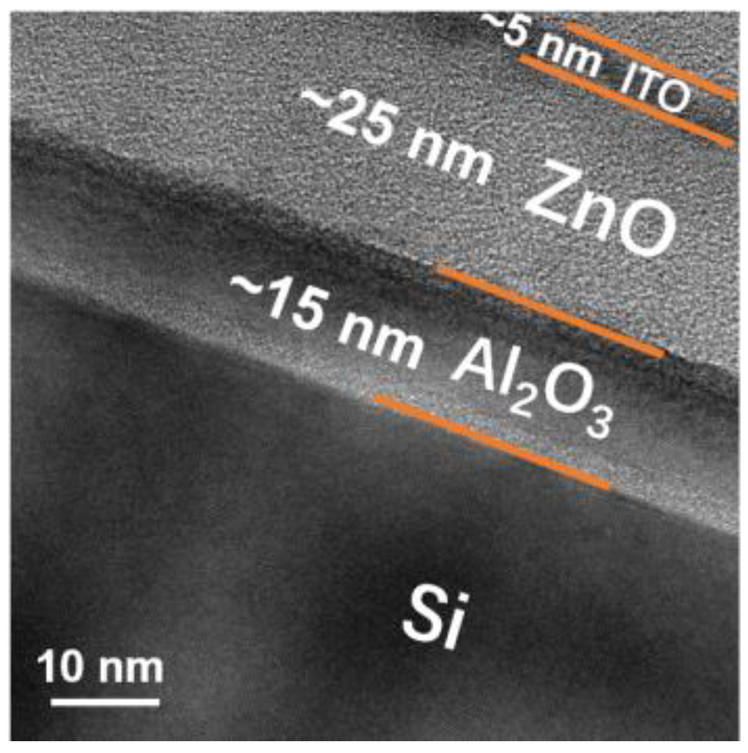
We conducted TEM measurement on the Al2O3/ZnO/ITO film, as shown in Figure 5. The figure shows that the Al2O3, ZnO, and ITO layers were stacked in order on Si substrate, and their respective thicknesses were about 15, 25, and 5 nm.
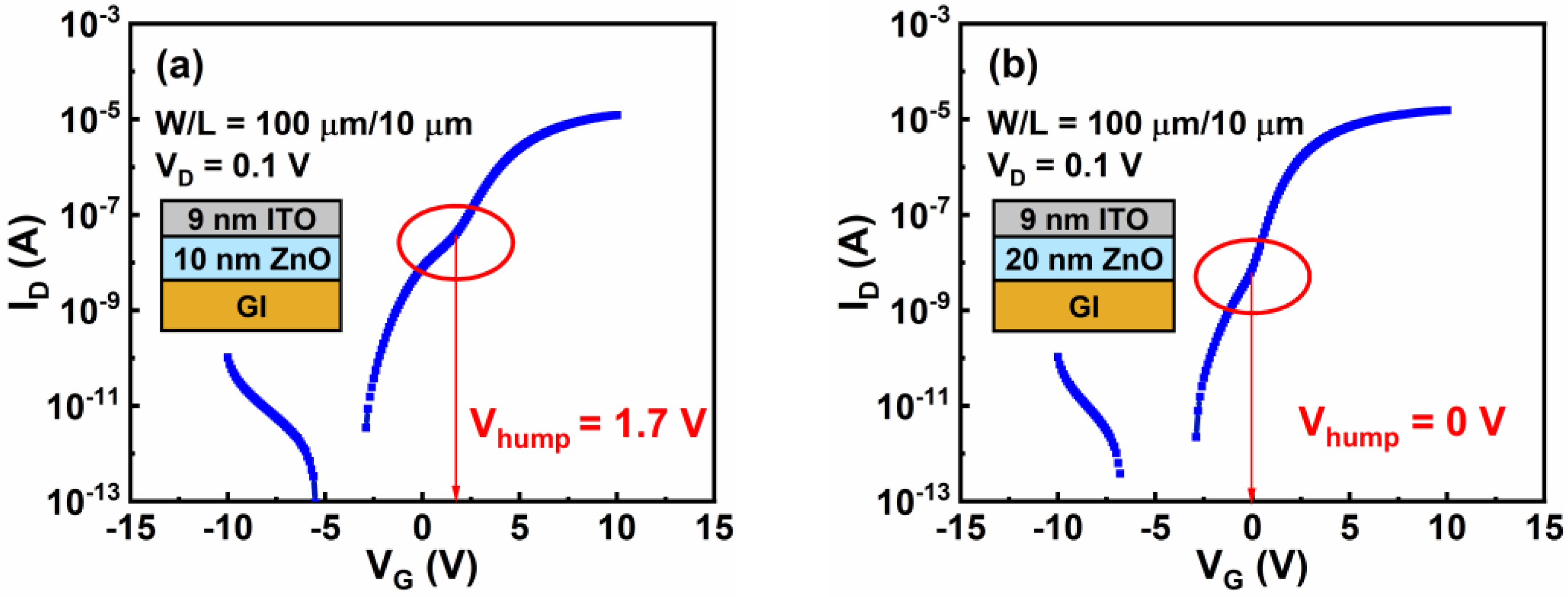
To investigate the effects of the thickness of the ZnO layer (tZnO) on the hump characteristics, drain current–gate voltage (ID–VG) curves of the group A TFTs were measured, as shown in Figure 6a–d. For the sake of brevity, Vhump, which is the gate voltage corresponding to occurrence of the hump, was marked by red ellipses. We found that Vhump negatively shifted from 1.7 to −0.7 V but VON remained nearly constant as tZnO increased from 10 to 40 nm. The parameters of the group A TFTs are listed in Table 2, including the field-effect mobility (µFE), Vhump, and VON.
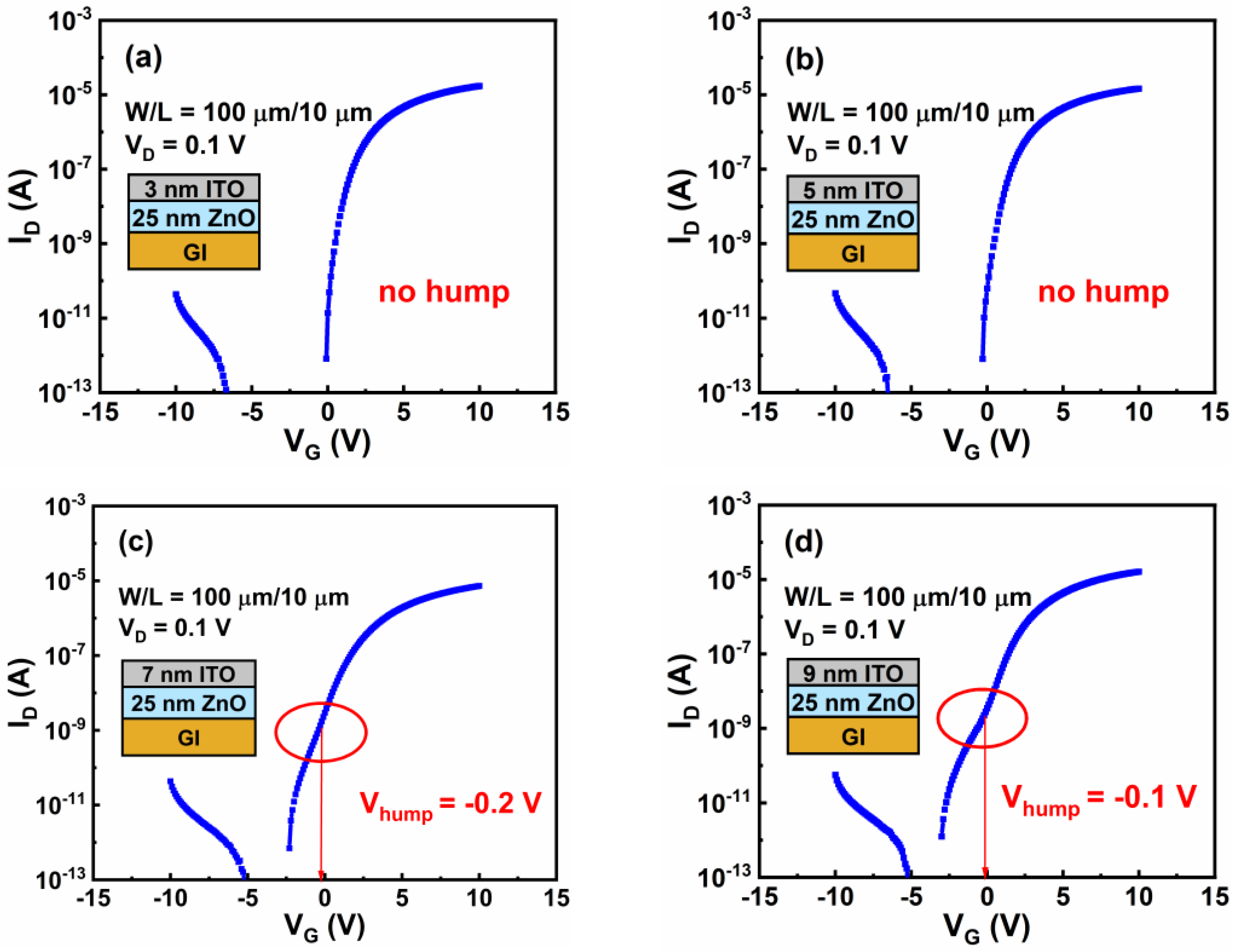
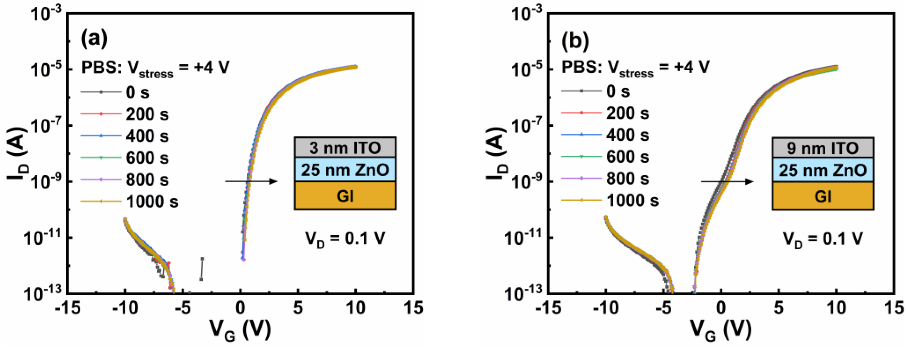
To explore the effects of the thickness of the ITO layer (tITO) on the hump characteristics, the ID–VG curves of the group B TFTs were also measured, as shown in Figure 7a–d. We can see that VON negatively shifted from −0.1 to −3 V as tITO increased from 3 to 9 nm. Clearly, TFTs with both 3-nm and 5-nm ITO layers showed no hump, so we defined their Vhump to be equal to VON values of −0.1 and −0.3 V, respectively. TFTs with 7-nm and 9-nm ITO layers, respectively, were found to have a Vhump of −0.2 V and −0.1 V. The parameters of the group B TFTs are also listed in Table 2. Based on the above results, it could be determined that Vhump depended on tZnO, while VON and μFE mainly depended on tITO.
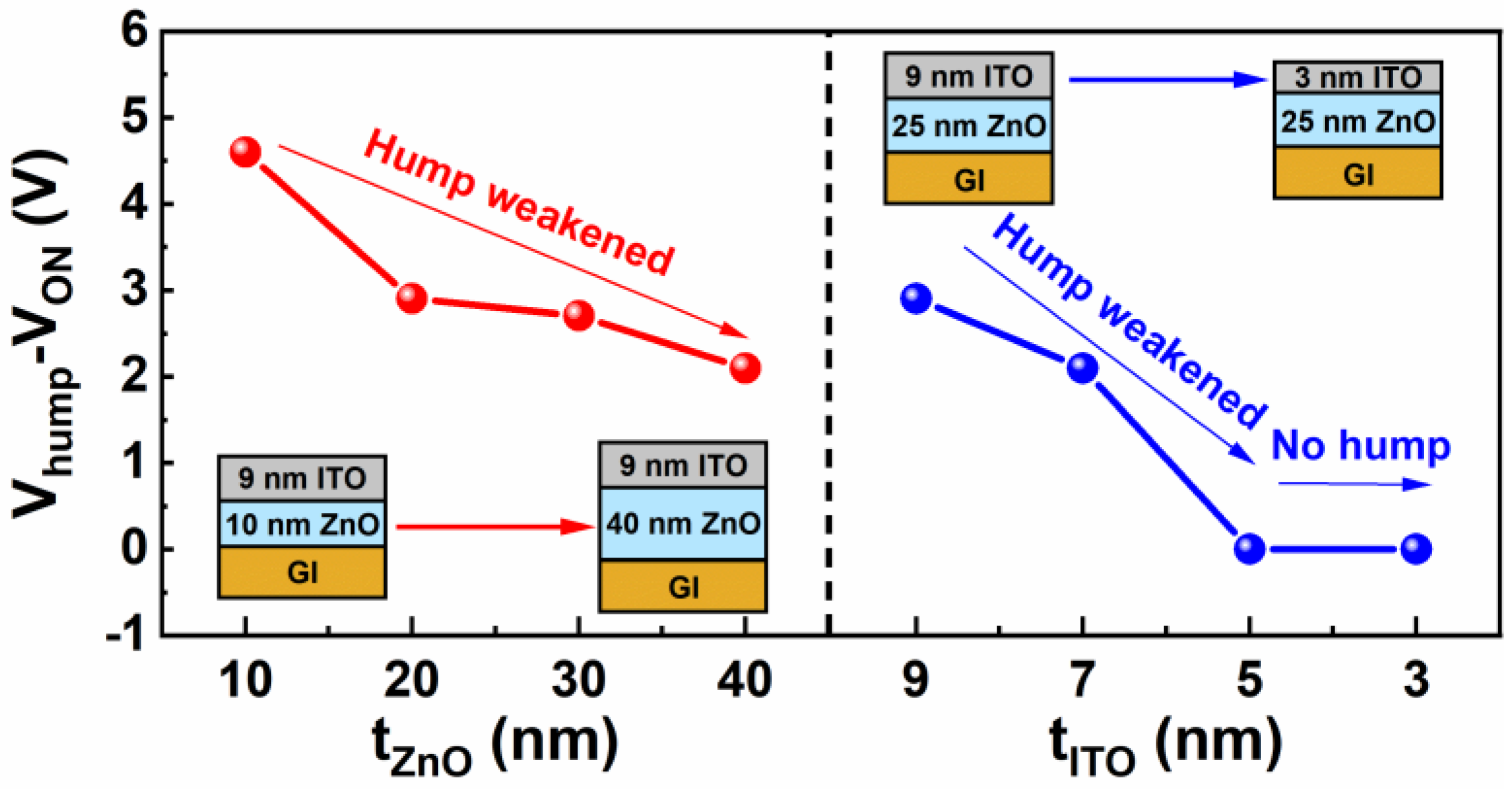
The value of Vhump–VON as a function of tZnO and tITO is depicted in Figure 8. We found that Vhump–VON, which is defined as an important parameter to measure the severity of hump phenomena, was negatively correlated with tZnO, but was positively correlated with tITO. Notably, by optimizing tITO ≤ 5 nm, the hump could be eliminated.
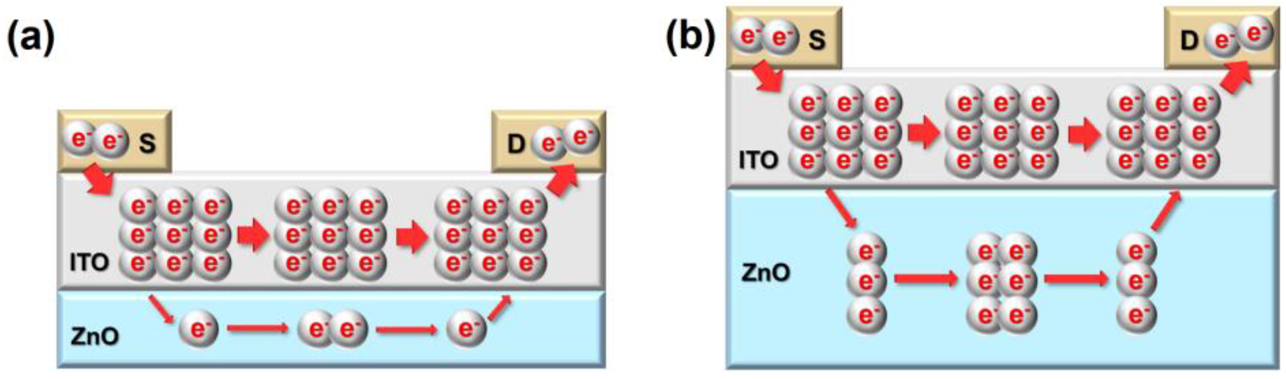
According to previous studies in the literature, the existence of two or more current paths is one of the important reasons leading to hump formation [12,16,18,21,29]. In this work, the generation of hump phenomena in ZnO/ITO TFTs should have resulted from the dual current paths through both the ZnO and ITO layers. Based on the experimental results, namely that Vhump depended on tZnO and VON depended on tITO, we could determine that the ITO current path turns on before the ZnO current path, at VGS = VON, while the ZnO current path turns on at VGS = Vhump.
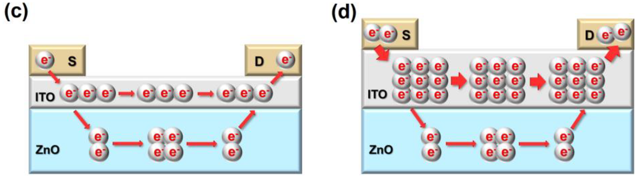
To provide the underlying mechanism of the hump characteristics of the ZnO/ITO TFTs, schematic diagrams that describe the current conduction in different channel structures are depicted, as shown in Figure 9a–d. For experimental group A, as tZnO increased from 10 to 40 nm, the carrier number in the ZnO layer increased and the Vhump was negatively shifted; thus, Vhump–VON presented a decreasing trend, and the hump was weakened. Nevertheless, as the total current was mainly affected by the ITO layer with high carrier concentration, the total current remained nearly constant and resulted in a stable μFE. For experimental group B, the current flowing through the ITO layer was improved as tITO increased, as shown in Figure 9c,d. Thereby, as tITO increased, VON was negatively shifted, μFE and Vhump–VON presented a positive correlation with tITO, and the hump was strengthened. Based on these results, it is clear that methods aimed at reducing the carrier concentration of the top channel layer—For example, adopting suitable post-processing treatment and optimizing process parameters—can be applied to suppress hump phenomena, and thus, these methods need further investigation.
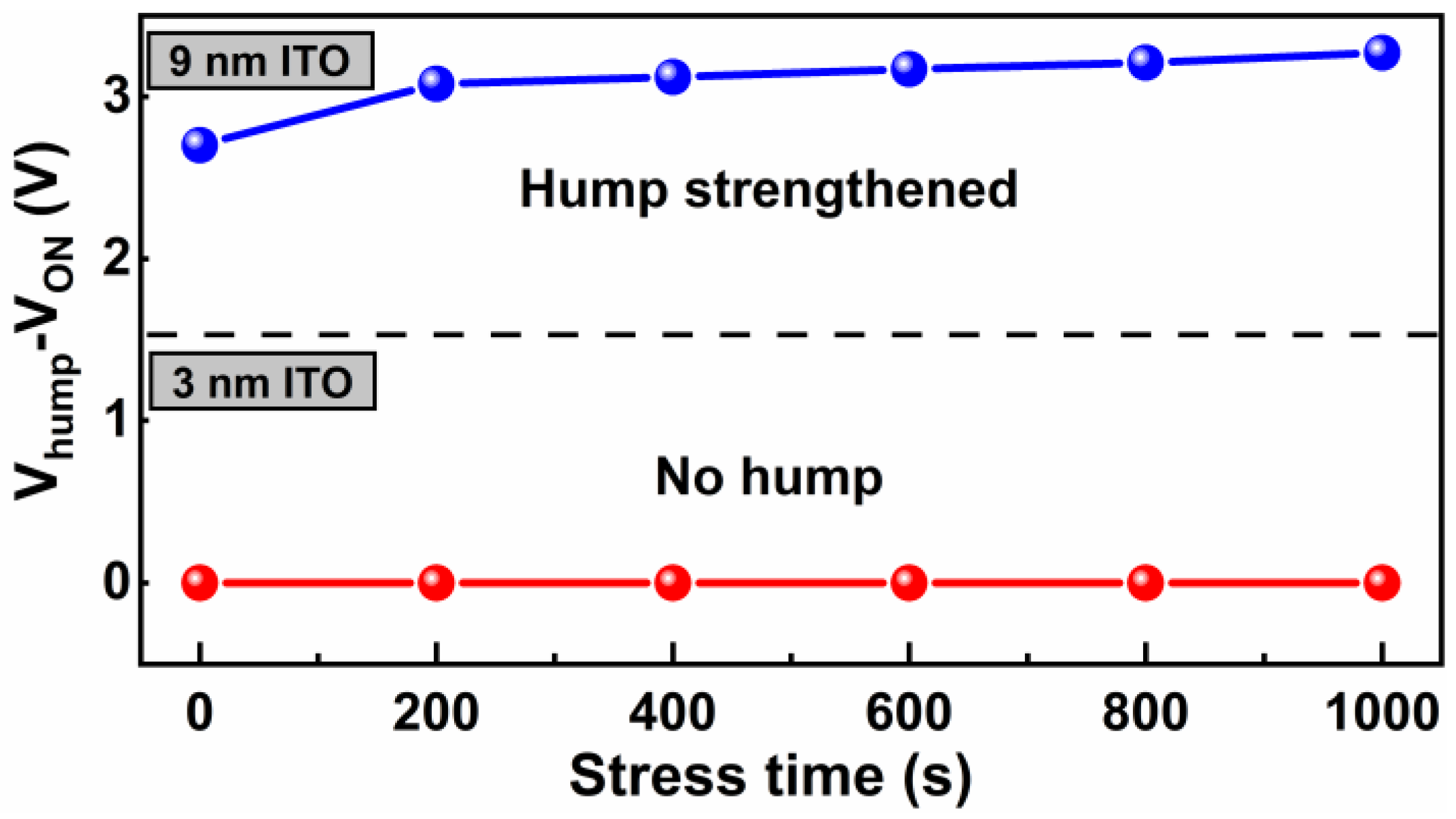
Considering that many reported hump phenomena are induced by PBS, the PBS dependence of the hump characteristics was also investigated. Figure 10 displays the effects of PBS on the transfer characteristics of group B TFTs with tITO of 3 and 9 nm, and the value of Vhump–VON plotted against stress time is shown in Figure 11. With increasing stress time, no hump was created for TFTs with tITO values of 3 nm, but the hump was strengthened for TFTs with tITO values of 9 nm. Under PBS, electrons were trapped in Al2O3 dielectric or/and at the Al2O3/ZnO interface, which influenced the shielding gate electric field [30,31]. When the tITO was 3 nm, VON and Vhump increased simultaneously with the stress time, so no hump occurred. When the tITO was 9 nm, Vhump increased but VON remained constant with stress time, and this was a result of the high carrier concentration of the ITO layer.
4. Conclusions
In conclusion, we first studied the material properties of the transparent conductive oxides ZnO and ITO. Further, we fabricated ZnO/ITO heterojunction TFTs and researched the effects of the channel structure on the hump characteristics. Our results showed that Vhump–VON negatively correlated with tZnO but positively correlated with tITO. In particular, the hump was eliminated when the tITO did not exceed 5 nm. Based on these results, current conduction in two channel layers is proposed to explain these hump characteristics. It was also found that the devices showed more severe humps under PBS for thicker ITO layers. This study extends the practical application of TCO and is helpful in terms of overcome the hump phenomenon of the oxide TFTs.
Author Contributions
Conceptualization and methodology, J.D. and Q.L.; data curation, J.D.; validation, D.H. and Y.W.; formal analysis, Y.W., resources, D.H.; investigation and writing—original draft preparation, Q.L.; software, D.X. and J.W.; project administration, D.H. All authors have read and agreed to the published version of the manuscript.
Funding
This research was funded by the National Natural Science Foundation of China, grant number 62004003.
Institutional Review Board Statement
Not applicable.
Informed Consent Statement
Not applicable.
Data Availability Statement
The data that support the findings of this study are available from the corresponding authors upon reasonable request.
Conflicts of Interest
The authors declare no conflict of interest.
References
- Fortunato, E.; Barquinha, P.; Martins, R. Oxide semiconductor thin-film transistors: A review of recent advances. Adv. Mater. 2012, 24, 2945–2986. [Google Scholar] [CrossRef] [PubMed]
- Shi, J.; Zhang, J.; Yang, L.; Qu, M.; Qi, D.C.; Zhang, K.H.L. Wide bandgap oxide semiconductors: From materials physics to optoelectronic devices. Adv. Mater. 2021, 33, e2006230. [Google Scholar] [CrossRef] [PubMed]
- Samanta, S.; Chand, U.; Xu, S.; Han, K.; Wu, Y.; Wang, C.; Kumar, A.; Velluri, H.; Li, Y.; Fong, X.; et al. Low subthreshold swing and high mobility amorphous Indium-Gallium-Zinc-Oxide thin-film transistor with thin HfO2 gate dielectric and excellent uniformity. IEEE Electron Device Lett. 2020, 41, 856–859. [Google Scholar] [CrossRef]
- Lee, S.Y. Comprehensive review on amorphous oxide semiconductor thin film transistor. Trans. Electr. Electron. Mater. 2020, 21, 235–248. [Google Scholar] [CrossRef]
- Li, H.; Han, D.; Yi, Z.; Dong, J.; Zhang, S.; Zhang, X.; Wang, Y. High-performance ZnO thin-film transistors prepared by atomic layer deposition. IEEE Trans. Electron Devices 2019, 66, 2965–2970. [Google Scholar] [CrossRef]
- Li, Q.; Dong, J.; Han, D.; Wang, Y. Effects of channel thickness on electrical performance and stability of high-performance InSnO thin-film transistors. Membranes 2021, 11, 929. [Google Scholar] [CrossRef]
- Park, J.C.; Lee, H.N. Improvement of the performance and stability of oxide semiconductor thin-film transistors using double-stacked active layers. IEEE Electron Device Lett. 2012, 33, 818–820. [Google Scholar] [CrossRef]
- Kim, J.I.; Ji, K.H.; Jung, H.Y.; Park, S.Y.; Choi, R.; Jang, M.; Yang, H.; Kim, D.H.; Bae, J.U.; Kim, C.D.; et al. Improvement in both mobility and bias stability of ZnSnO transistors by inserting ultra thin InSnO layer at the gate insulator/channel Interface. Appl. Phys. Lett. 2011, 99, 122102. [Google Scholar] [CrossRef]
- Furuta, M.; Koretomo, D.; Magari, Y.; Aman, S.G.M.; Higashi, R.; Hamada, S. Heterojunction channel engineering to enhance performance and reliability of amorphous In–Ga–Zn–O thin-film transistors. Jpn. J. Appl. Phys. 2019, 58, 090604. [Google Scholar] [CrossRef]
- Yang, J.; Liao, P.Y.; Chang, T.C.; Chen, B.W.; Huang, H.C.; Chiang, H.C.; Su, W.C.; Zhang, Q. Investigation of a hump phenomenon in back-channel-etched amorphous In-Ga-Zn-O thin-film transistors under negative bias stress. IEEE Electron Device Lett. 2017, 38, 592–595. [Google Scholar] [CrossRef]
- Choi, S.H.; Han, M.K. Effect of channel widths on negative shift of threshold voltage, including stress-induced hump phenomenon in InGaZnO thin-film transistors under high-gate and drain bias stress. Appl. Phys. Lett. 2012, 100, 043503. [Google Scholar] [CrossRef] [Green Version]
- Tsai, Y.S.; Chen, J.Z. Positive gate-bias temperature stability of RF-sputtered Mg0.05Zn0.95O active-layer thin-film transistors. IEEE Trans. Electron Devices 2012, 59, 151–158. [Google Scholar] [CrossRef]
- Lee, J.H.; Ahn, C.H.; Hwang, S.; Woo, C.H.; Park, J.-S.; Cho, H.K.; Lee, J.Y. Role of the crystallinity of ZnO films in the electrical properties of bottom-gate thin film transistors. Thin Solid Films 2011, 519, 6801–6805. [Google Scholar] [CrossRef]
- Lee, J.Y.; Lee, S.Y. Investigation on hump mechanism in amorphous SiZnSnO thin-film transistor depending on Si concentration. Phys. Status Solidi A 2020, 217, 1900953. [Google Scholar] [CrossRef]
- Valletta, A.; Gaucci, P.; Mariucci, L.; Fortunato, G.; Templier, F. “Hump” characteristics and edge effects in polysilicon thin film transistors. J. Appl. Phys. 2008, 104, 124511. [Google Scholar] [CrossRef]
- Teng, T.; Hu, C.F.; Qu, X.P.; Wang, M. Investigation of the anomalous hump phenomenon in amorphous InGaZnO thin-film transistors. Solid State Electron. 2020, 170, 107814. [Google Scholar] [CrossRef]
- Chen, H.C.; Chen, J.J.; Tu, Y.F.; Zhou, K.J.; Kuo, C.W.; Su, W.C.; Hung, Y.H.; Shih, Y.S.; Huang, H.C.; Tsai, T.M.; et al. Abnormal hump effect induced by hydrogen diffusion during self-heating stress in top-gate amorphous InGaZnO TFTs. IEEE Trans. Electron Devices 2020, 67, 2807–2811. [Google Scholar] [CrossRef]
- Kim, W.S.; Cho, Y.J.; Lee, Y.H.; Park, J.; Kim, G.; Kim, O. Abnormal behavior with hump characteristics in current stressed a-InGaZnO thin film transistors. Solid State Electron. 2017, 137, 22–28. [Google Scholar] [CrossRef]
- Hsieh, S.; Liang, H.Y.; Lin, C.J.; King, Y.C. Stress-induced width-dependent degradation of low-temperature polycrystalline silicon thin-film transistor. Appl. Phys. Lett. 2007, 90, 183502. [Google Scholar] [CrossRef] [Green Version]
- Kim, Y.M.; Jeong, K.S.; Yun, H.J.; Yang, S.D.; Lee, S.Y.; Lee, H.D.; Lee, G.W. Electrical instabilities in amorphous InGaZnO thin film transistors with Si3N4 and Si3N4/Al2O3 Gate Dielectrics. Jpn. J. Appl. Phys. 2012, 51, 09MF10. [Google Scholar] [CrossRef]
- Maeng, W.J.; Park, J.S.; Kim, H.S.; Kim, E.S.; Son, K.S.; Kim, T.S.; Ryu, M.; Lee, S. The effect of active-layer thickness and back-channel conductivity on the subthreshold transfer characteristics of Hf-In-Zn-O TFTs. IEEE Electron Device Lett. 2011, 32, 1077–1079. [Google Scholar] [CrossRef]
- Zhao, M.; Zhang, Z.; Xu, Y.; Xu, D.; Zhang, J.; Huang, Z. High-performance back-channel-etched thin-film transistors with an InGaO/InZnO stacked channel. Phys. Status Solidi A 2020, 217, 1900773. [Google Scholar] [CrossRef]
- Zhao, K.; Xie, J.; Zhao, Y.; Han, D.; Wang, Y.; Liu, B.; Dong, J. Investigation on transparent, conductive ZnO: Al films deposited by atomic layer deposition process. Nanomaterials 2022, 12, 172. [Google Scholar] [CrossRef] [PubMed]
- Barreca, D.; Garon, S.; Tondello, E.; Zanella, P. SnO2 nanocrystalline thin films by XPS. Surf. Sci. Spectra 2000, 7, 81–85. [Google Scholar] [CrossRef]
- Jung, H.Y.; Kang, Y.; Hwang, A.Y.; Lee, C.K.; Han, S.; Kim, D.-H.; Bae, J.-U.; Shin, W.-S.; Jeong, J.K. Origin of the improved mobility and photo-bias stability in a double-channel metal oxide transistor. Sci. Rep. 2014, 4, 3765. [Google Scholar] [CrossRef] [Green Version]
- Saha, J.K.; Billah, M.M.; Jang, J. Triple-stack ZnO/AlZnO/YZnO heterojunction oxide thin-film transistors by spray pyrolysis for high mobility and excellent stability. ACS Appl. Mater. Interfaces 2021, 13, 37350–37362. [Google Scholar] [CrossRef]
- Kamiya, T.; Nomura, K.; Hosono, H. Origins of high mobility and low operation voltage of amorphous oxide TFTs: Electronic structure, electron transport, defects and doping. J. Disp. Technol. 2009, 5, 273–288. [Google Scholar] [CrossRef]
- Choi, K.H.; Kim, H.K. Correlation between Ti source/drain contact and performance of InGaZnO-based thin film transistors. Appl. Phys. Lett. 2013, 102, 052103. [Google Scholar] [CrossRef] [Green Version]
- Jeong, K.S.; Kim, Y.M.; Lee, G.W. Origin of oxygen-induced abnormal hump in bottom-gated polycrystalline zinc oxide thin film transistors. ECS J. Solid State Sci. Technol. 2015, 4, Q31–Q34. [Google Scholar] [CrossRef]
- Choi, S.; Choi, S.J.; Kim, D.H.; Park, S.; Kim, J.; Seo, Y.; Shin, H.J.; Jeong, Y.S.; Bae, J.U.; Oh, C.H.; et al. Positive bias stress instability of InGaZnO TFTs with self-aligned top-gate structure in the threshold-voltage compensated pixel. IEEE Electron Device Lett. 2020, 41, 50–53. [Google Scholar] [CrossRef]
- Yang, J.; Liao, P.Y.; Chang, T.C.; Chen, B.W.; Huang, H.C.; Su, W.C.; Chiang, H.C.; Zhang, Q. H2O adsorption on amorphous In-Ga-Zn-O thin-film transistors under negative bias stress. Appl. Phys. Lett. 2017, 110, 143508. [Google Scholar] [CrossRef]
Figure 1.
Schematic of the ZnO/ITO TFTs used in this article.

Figure 2.
(a) Transmittance of ZnO and ITO films. (αhν)2-hν curves of (b) ZnO and (c) ITO films. ZnO and ITO films were deposited on glass substrates.
Figure 2.
(a) Transmittance of ZnO and ITO films. (αhν)2-hν curves of (b) ZnO and (c) ITO films. ZnO and ITO films were deposited on glass substrates.

Figure 3.
XPS spectra of (a) ZnO and (b) ITO films. ZnO and ITO films were deposited on Si substrates.
Figure 3.
XPS spectra of (a) ZnO and (b) ITO films. ZnO and ITO films were deposited on Si substrates.

Figure 4.
AFM images of (a) ZnO and (b) ITO films. ZnO and ITO films were deposited on Si substrates.
Figure 4.
AFM images of (a) ZnO and (b) ITO films. ZnO and ITO films were deposited on Si substrates.

Figure 5.
Cross-sectional TEM image of the Al2O3/ZnO/ITO film. Al2O3/ZnO/ITO film was deposited on Si substrate.
Figure 5.
Cross-sectional TEM image of the Al2O3/ZnO/ITO film. Al2O3/ZnO/ITO film was deposited on Si substrate.

Figure 6.
ID–VG curves for group A TFTs. The tZnO values are (a) 10 nm, (b) 20 nm, (c) 30 nm, and (d) 40 nm. The tITO value is 9 nm.
Figure 6.
ID–VG curves for group A TFTs. The tZnO values are (a) 10 nm, (b) 20 nm, (c) 30 nm, and (d) 40 nm. The tITO value is 9 nm.


Figure 7.
ID–VG curves for group B TFTs. The tITO values are (a) 3 nm, (b) 5 nm, (c) 7 nm, and (d) 9 nm. The tZnO value is 25 nm.
Figure 7.
ID–VG curves for group B TFTs. The tITO values are (a) 3 nm, (b) 5 nm, (c) 7 nm, and (d) 9 nm. The tZnO value is 25 nm.

Figure 8.
Vhump–VON versus tZnO and tITO.

Figure 9.
Schematic diagrams of current conduction in channel structures of (a) ZnO/ITO (10 nm/9 nm), (b) ZnO/ITO (40 nm/9 nm), (c) ZnO (25 nm)/ITO (≤5 nm), and (d) ZnO (25 nm)/ITO (>5 nm).
Figure 9.
Schematic diagrams of current conduction in channel structures of (a) ZnO/ITO (10 nm/9 nm), (b) ZnO/ITO (40 nm/9 nm), (c) ZnO (25 nm)/ITO (≤5 nm), and (d) ZnO (25 nm)/ITO (>5 nm).


Figure 10.
PBS stability for ZnO/ITO TFTs with tITO values of (a) 3 and (b) 9 nm. The tZnO is 25 nm.
Figure 10.
PBS stability for ZnO/ITO TFTs with tITO values of (a) 3 and (b) 9 nm. The tZnO is 25 nm.

Figure 11.
Vhump–VON versus PBS time for ZnO/ITO TFTs with tITO values of 3 and 9 nm. The tZnO value is 25 nm.
Figure 11.
Vhump–VON versus PBS time for ZnO/ITO TFTs with tITO values of 3 and 9 nm. The tZnO value is 25 nm.


Table 1.
Hall-effect results of ZnO and ITO films. ZnO and ITO films were deposited on glass substrates.
Table 1.
Hall-effect results of ZnO and ITO films. ZnO and ITO films were deposited on glass substrates.
| Sample | Carrier Concentration (cm−3) | Conductivity (Ω−1cm−1) |
|---|---|---|
| ZnO | 1.63 × 10¹⁶ | 1.78 × 10⁻² |
| ITO | 2.80 × 10¹⁹ | 78.91 |
Table 2.
Electrical parameters of ZnO/ITO TFTs, including µFE, Vhump, and VON.
| tZnO (nm) | µFE (cm2/Vs) | Vhump (V) | VON (V) | |
| Group A | 10 | 10.71 | 1.7 | −2.9 |
| 20 | 11.28 | 0 | −2.9 | |
| 30 | 12.55 | −0.1 | −2.8 | |
| 40 | 12.31 | −0.7 | −2.8 | |
| tITO (nm) | µFE (cm2/Vs) | Vhump (V) | VON (V) | |
| Group B | 3 | 13.06 | −0.1 | −0.1 |
| 5 | 15.69 | −0.3 | −0.3 | |
| 7 | 18.30 | −0.2 | −2.3 | |
| 9 | 18.64 | −0.1 | −3.0 |
Publisher’s Note: MDPI stays neutral with regard to jurisdictional claims in published maps and institutional affiliations. |
© 2022 by the authors. Licensee MDPI, Basel, Switzerland. This article is an open access article distributed under the terms and conditions of the Creative Commons Attribution (CC BY) license (https://creativecommons.org/licenses/by/4.0/).
Share and Cite
MDPI and ACS Style
Li, Q.; Dong, J.; Han, D.; Xu, D.; Wang, J.; Wang, Y. Structural Engineering Effects on Hump Characteristics of ZnO/InSnO Heterojunction Thin-Film Transistors. Nanomaterials 2022, 12, 1167. https://doi.org/10.3390/nano12071167
AMA Style
Li Q, Dong J, Han D, Xu D, Wang J, Wang Y. Structural Engineering Effects on Hump Characteristics of ZnO/InSnO Heterojunction Thin-Film Transistors. Nanomaterials. 2022; 12(7):1167. https://doi.org/10.3390/nano12071167
Chicago/Turabian StyleLi, Qi, Junchen Dong, Dedong Han, Dengqin Xu, Jingyi Wang, and Yi Wang. 2022. "Structural Engineering Effects on Hump Characteristics of ZnO/InSnO Heterojunction Thin-Film Transistors" Nanomaterials 12, no. 7: 1167. https://doi.org/10.3390/nano12071167
Note that from the first issue of 2016, this journal uses article numbers instead of page numbers. See further details here.