Article

Fabrication of Porous Lead Bromide Films by Introducing Indium Tribromide for Efficient Inorganic CsPbBr3 Perovskite Solar Cells

1
State Key Laboratory of Superhard Materials, College of Physics, Jilin University, Changchun 130012, China
2
School of Science, Northeast Electric Power University, Jilin 132012, China
3
Beijing Key Lab of Cryo-Biomedical Engineering and Key Lab of Cryogenics, Technical Institute of Physics and Chemistry, Chinese Academy of Sciences, Beijing 100190, China
4
College of Physics, Jilin University, Changchun 130012, China
*
Authors to whom correspondence should be addressed.
Nanomaterials 2021, 11(5), 1253; https://doi.org/10.3390/nano11051253
Submission received: 21 April 2021 / Revised: 5 May 2021 / Accepted: 8 May 2021 / Published: 11 May 2021
(This article belongs to the Special Issue Nanostructures for Perovskite Solar Cells and Light-Emitting Diodes)

Abstract

:
In the process of preparing CsPbBr3 films by two-step or multi-step methods, due to the low solubility of CsBr in organic solvents, the prepared perovskite films often have a large number of holes, which is definitely not conducive to the performance of CsPbBr3 perovskite solar cells (PSCs). In response to this problem, this article proposed a method of introducing InBr3 into the PbBr2 precursor to prepare a porous PbBr2 film to increase the reaction efficiency between CsBr and PbBr2 and achieve the purpose of In (Ⅲ) incorporation, which not only optimized the morphology of the produced CsPbBr3 film but also enhanced the charge extraction and transport capabilities, which was ascribed to the reduction of the trap state density and impurity phases in the perovskite films, improving the performance of CsPbBr3 PSCs. At the optimal InBr3 concentration of 0.21 M, the InBr3:CsPbBr3 perovskite solar cell exhibited a power conversion efficiency of 6.48%, which was significantly higher than that of the pristine device.

1. Introduction

After more than ten years of rapid development, lead halide-based perovskite solar cells have made remarkable achievements, but they seem to be in a vicious circle where high efficiency and high stability are contradictory to each other. Although the power conversion efficiency (PCE) of organic-inorganic hybrid perovskite solar cells (PSCs) has increased from the initial 3.8% to more than 25% at present [1,2,3,4,5], yet due to the strong volatility of common A-site organic cations, such as organic methylammonium (MA+) and formamidinium (FA+), the organic components disappear under thermal stress [6,7]. In terms of thermal stability, the all-inorganic cesium-lead halide perovskite CsPbX3 (X: iodine or bromine), which is formed by using more stable inorganic cesium ions (Cs+) to completely replace organic cations, usually performs better stability [8,9,10,11] and is not prone to degradation at temperatures above 400 °C [8,12]. This provides the necessary conditions for the long-term stable use of CsPbX3 PSCs [13,14,15,16]. The key factor, which influences the stability of CsPbX3, is the moisture in the air. The presence of humidity changes the phase of the perovskite and reduces the stability of the photovoltaic device, but this does not directly cause the decomposition of CsPbX3 (mainly I-rich CsPbX3) and the lack of components [8,17,18]. Of course, this phase change is reversible when heated [19].
Compared with other Cs-based inorganic perovskites, the most prominent advantage of CsPbBr3 is that it has a highly stable crystal structure. Whether it is the orthorhombic γ-phase at room temperature or tetragonal β-phase and cubic α-phase when heated, the geometric structures of CsPbBr3 have not changed much, so the electronic structures of different phases are also relatively similar [20]. For this reason, CsPbBr3 is also regarded as a perovskite material that presents better stability to humidity, heat, and light at ambient temperature [2,8,21,22]. Since Kulbak et al. first prepared the CsPbBr3 PSCs by a two-step solution-processing method in 2015 [22], in less than ten years, the PCE of the CsPbBr3 based PSCs have reached more than 10% with an ultrahigh open-circuit voltage (VOC) of 1.62 V [23], but it still has a large distance compared with CsPbBr3 PSCs theoretical limit PCE of 16.4% [24] and the maximized PCE of 19.0% for inorganic CsPbI3 PSCs [10].
In the process of preparing CsPbBr3 PSCs by the solution-processing method, the solubility of CsBr in commonly used polar solvents is poor, and the concentration differences between CsBr and PbBr2 solutions are large, which leads to the derivative phases PbBr2-rich CsPb2Br5 and CsBr-rich Cs4PbBr6 in the process of the generation of CsPbBr3 [25]. At the same time, the thickness of the non-optimized prepared perovskite film is low, and the ability to absorb light is inadequate; numerous pinholes appear in the film [26]. Consequently, a decrease appears in the PCE of CsPbBr3 PSCs. Regardless of whether it is a two-step sequential deposition or a multi-step method to prepare CsPbBr3, it is necessary to deposit PbBr2 first and then use CsBr to convert PbBr2 to CsPbBr3. Improving the PbBr2 film preparation process and adjusting the PbBr2 preparation method can achieve the goals of enhancing the reaction efficiency of the precursor, accurately controlling the subsequent growth of CsPbBr3 crystals, and reducing the generation of by-products, and finally obtain perovskite film with a high purity phase, large grain size, and high coverage [23,27]. By precisely regulating the film-forming temperature and pore diameter of the PbBr2 precursor film, Zhao et al. [23] minimized the compressive stress of the perovskite film and prepared CsPbBr3 grains with a size of up to 1.62 μm, which not only made the PCE of the all-inorganic CsPbBr3 perovskite solar cell reach 10.7%, the open-circuit voltage (VOC) as high as 1.6 V, and it also kept the device extremely stable in a high-humidity air environment. Lee et al. [28] introduced CZISSE QDs quantum dots into the PbBr2 film. CZISSE QDs acted as seeds to promote the crystallization of CsPbBr3 and, at the same time, penetrated into the m-TiO2 and CsPbBr3 perovskite films to increase the electron extraction and transportability of TiO2, thereby improving the conversion efficiency of the device by 20.6%.
In this work, InBr3 was introduced into the PbBr2 precursor solution, so that the multiple ordered crystal orientations of lead bromide grew, and the original rough and extremely uneven grain distribution of the PbBr2 film evolved into a large uniform-porous film with pores. This morphological change ensured the full diffusion and uniform reaction of CsBr in the PbBr2 film during the synthesis of CsPbBr3 and was conducive to the formation of polycrystalline surface growth, high purity phase, and uniform morphology InBr3: CsPbBr3 film. The PCE of the small area (0.09 cm2) InBr3:CsPbBr3 PSC obtained after conditions optimization was 6.48%, in particular, the VOC was significantly improved.

2. Experiment Section

2.1. Materials

PbBr2 (99.99%) and CsBr (99.9%) were purchased from Xi’an Polymer Light Technology Corp. (Xi’an, China) and were not purified. InBr3 (99.9%) was purchased from Shanghai Macklin Biochemical Co., Ltd. (Shanghai, China). Titanium diisopropoxide bis (acetylacetonate; 75 wt% in 2-propanol) was purchased from Sigma-Aldrich (Louis, MO, USA). Titanium dioxide (TiO2) paste (18 NR-T) was purchased from Greatcell Solar Limited (Queanbeyan, Australia). N,N-Dimethylformamide (DMF, chromatographic grade, ≥99.9%), methanol (chromatographic grade, ≥99.9%), ethanol (chromatographic grade, ≥99.8%), and isopropanol (≥99.5%) were purchased from Aladdin (Shanghai, China). The fluorine-doped tin oxide coated glass (FTO, 6 Ω/□) and carbon paste were purchased from Opvtech New Energy Co., Ltd. (Yingkou, China) and Shanghai MaterWin New Materials Co., Ltd. (Shanghai, China), respectively.

2.2. Device Fabrication

All the following processes were carried out in a fume hood environment, without artificial control of the temperature, humidity, and airflow rate of the surrounding environment. The fluorine-doped tin-oxide-coated glasses were patterned by laser etching and cleaned by ultrasonic with acetone, isopropanol, ethanol, and deionized water. After being dried by high purity nitrogen, the FTO were further cleaned by an ultrasound treatment for 15 min and washed with ethanol. Afterward, the pre-conditioned FTO were spin-coated with 0.15 M titanium diisopropoxide bis(acetylacetonate) in 1-butanol at 5000 rpm for 20 s and were heated at 125 °C for 5 min. After these substrates returned to room temperature, the above procedure was repeated twice with 0.3 M titanium diisopropoxide bis(acetylacetonate) in 1-butanol and compact TiO2 (c-TiO2) was obtained. After that, the mesoporous TiO2 (m-TiO2) films were deposited on the above cooling c-TiO2 by spin-coating at 5000 rpm for 30 s by means of TiO2 paste diluted with ethanol. Further, the obtained layers were dried at 125 °C for 5 min followed by the muffle furnace at 500 °C for 30 min. After the muffle furnace was lowered to room temperature, pre-coated substrates were acquired.
Perovskite films were synthesized by a multistep solution-processing method. 0.03, 0.09, 0.15, 0.21, and 0.27 mmol InBr3 were added into 1 mL DMF of PbBr2 (1 M) and stirred. After the InBr3 was completely dissolved, the DMF mixed solution was spin-coated on pre-coated substrates at 2000 rpm for 30 s and then heated to 90 °C for 30 min. Afterward, the methanol solution of CsBr (0.07 M) was spin-coated on the InBr3:PbBr2 film at 5000 rpm for 30 s and heated to 250 °C for 5 min, and this step was repeated five times. Next, the prepared sample was placed in isopropanol and soaked for 30 min and annealed at 250 °C for 15 min to remove excess CsBr. Finally, the carbon paste was deposited coated on the perovskite films by using the doctor blade coating method and dried at 100 °C for 10 min. The effective area of the back electrode was 3 mm × 3 mm, which defined the active area of each device.

2.3. Characterization

The morphologies of the synthesized films and energy-dispersive X-ray spectroscopy (EDS) mapping images were observed by a scanning electron microscope (SEM, FEI MAGELLAN 400, FEI, Hillsboro, OR, USA). The crystal structure of the synthesized sample was determined by means of X-ray diffraction (XRD, Cu Kα radiation, λ = 1.5418 Å, Rigaku D/max2500, Tokyo, Japan). The steady-state photoluminescence (PL) spectra of perovskite films were performed using a Renishaw InVia micro-Raman spectroscopy system (Renishaw, Wotton-under-Edge, UK) with a 473 nm excitation source. Ultraviolet photoelectron (UPS) and X-ray photoelectron spectroscopy (XPS) were carried out by an X-ray photoelectron spectrometer (EscaLab Xi+, Thermofisher, Waltham, MA, USA). UV-Vis spectrometer (UV-3600, Shimadzu, Kyoto, Japan) was employed to measure the absorption spectrum in the range of 200 nm to 800 nm. The current-voltage (J–V) characteristics and the external quantum efficiency (EQE) of the fabricated solar devices were measured by a solar cells test system (XP3000, Sanyou, Beijing, China) and an EQE measured system (QTest Station 1000A, CROWNTECH, Inc., Macungie, PA, USA), respectively. The impedance was executed at 10−1~107 Hz by using an impedance analyzer in a dark environment (Solartron 1260 coupled to the dielectric interface 1296, Farnborough, UK).

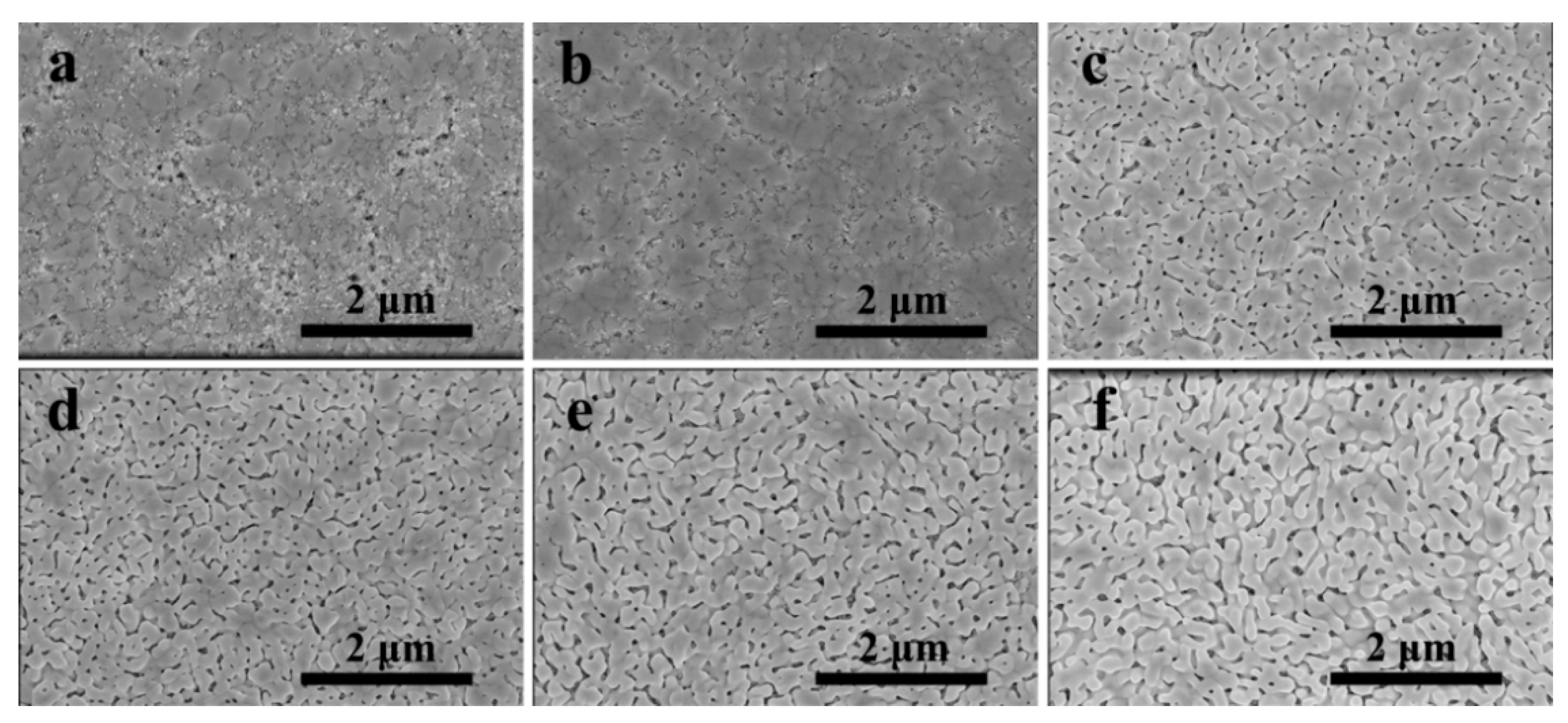
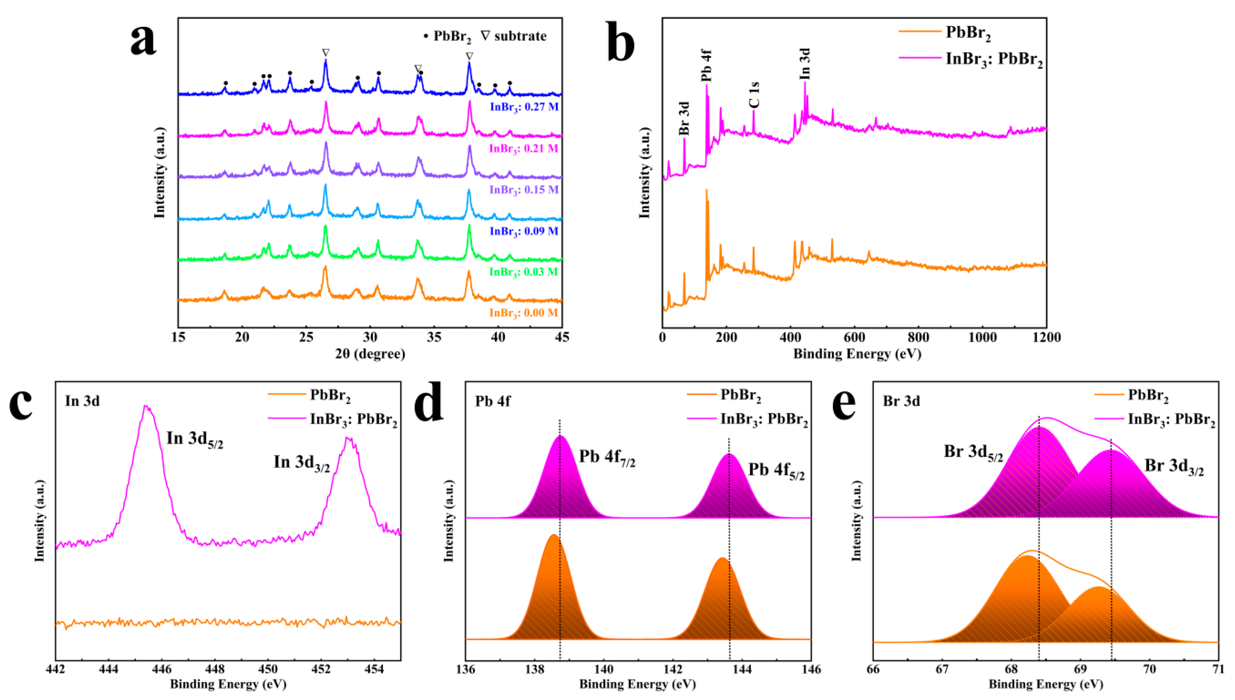
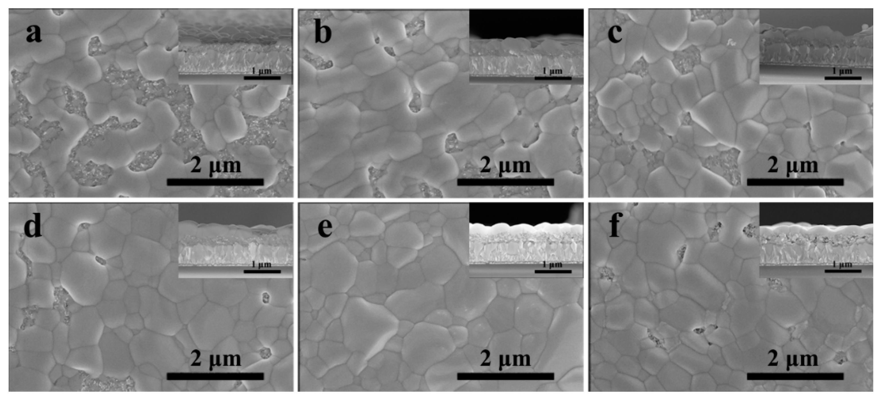
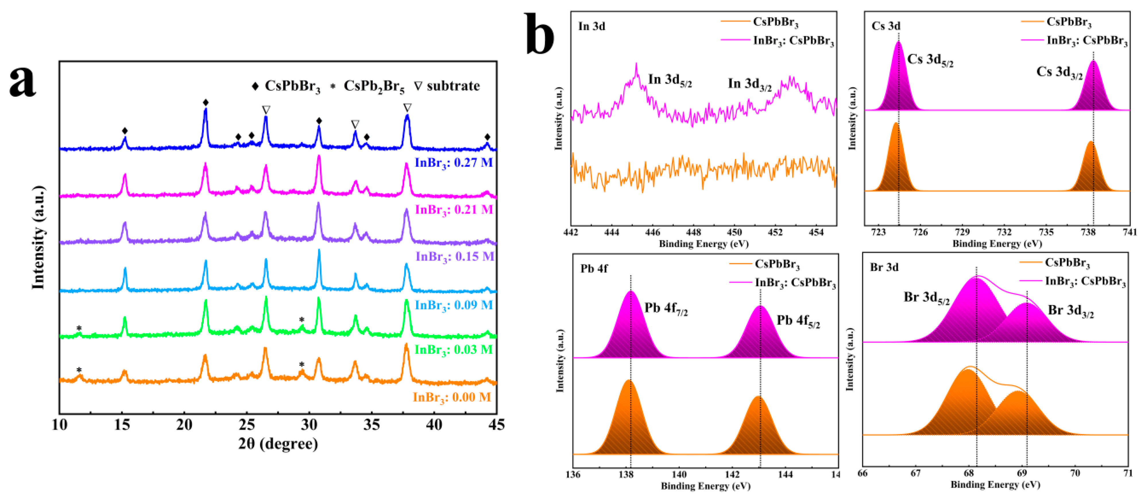
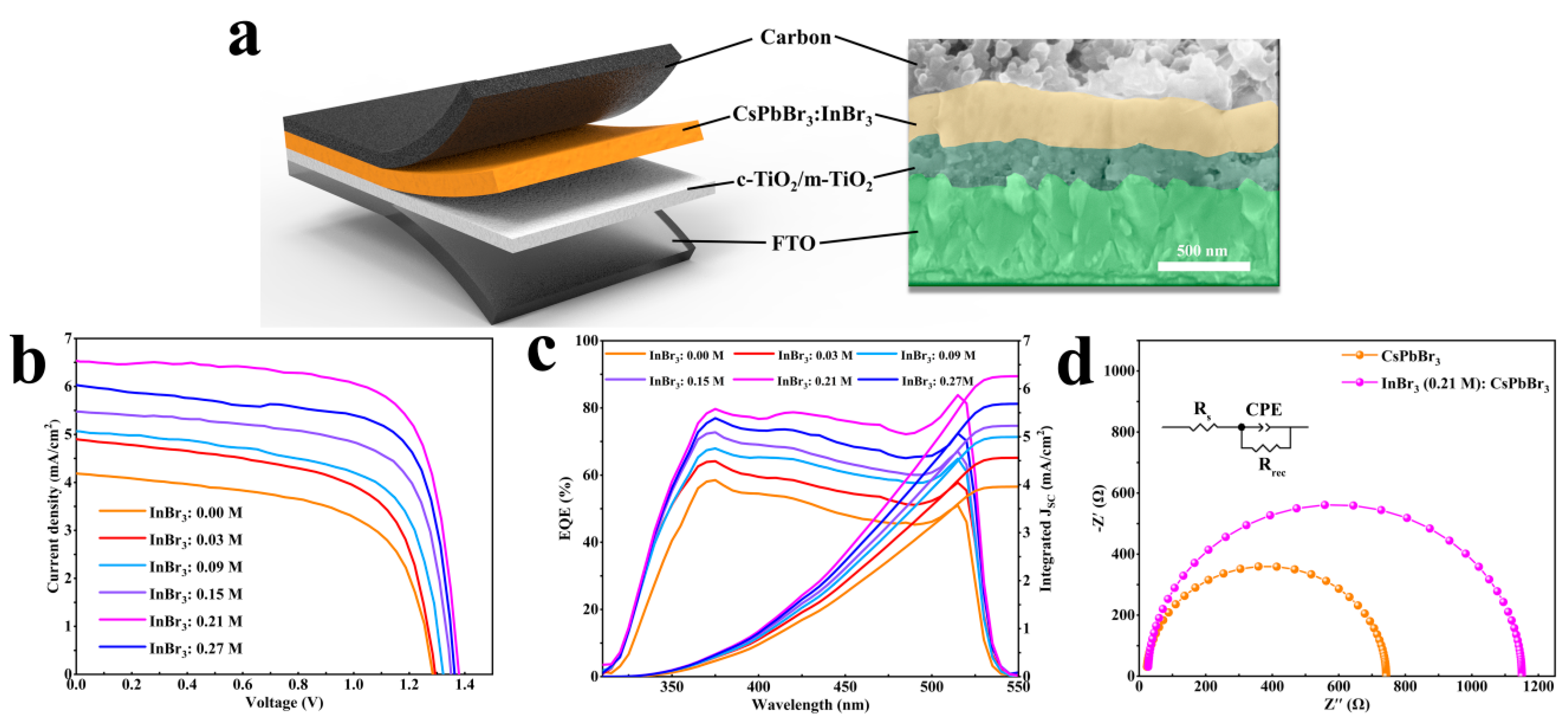
3. Results and Discussion

In the two-step or multi-step method of preparation of perovskite, the quality of the PbBr2 film determined the morphology of the following perovskite film. Figure 1 shows the top-view SEM images of PbBr2 films by introducing different concentrations of InBr3. When there was no InBr3 in the PbBr2 precursor solution, as shown in Figure 1a, the surface of the obtained sample was rough, and the PbBr2 grain distribution was extremely uneven, and a large area of exposed m-TiO2 could be directly observed. When the PbBr2 precursor solution was introduced into 0.03 M InBr3, as shown in Figure 1b, the surface of the PbBr2 film was flat, and the coverage of the m-TiO2 film was increased, and the observable exposed m-TiO2 area was significantly reduced. With the gradual increase in the concentration of introduced InBr3 (Figure 1c–f), the PbBr2 film appeared porous, but the number of pores decreased as the concentration of InBr3 increased. Meanwhile, the porosity volume increased as the concentration of InBr3 increased. From the cross-sectional view of PbBr2 shown in Figure S1 (Supplementary Materials), we could clearly see that the pure PbBr2 film has a flat surface and a uniform thickness of about 50~60 nm, and the m-TiO2 was filled with PbBr2. As the concentration of InBr3 introduced gradually increased, the thickness of the PbBr2 film also gradually increased (about 70 nm, 90 nm, 100 nm, 120 nm, 160 nm), and the film roughness increased. The above data could clearly demonstrate that the introduction of InBr3 could effectively affect the morphology of the PbBr2 film. The increase in the porosity volume, roughness, and thickness of the PbBr2 film facilitated the diffusion of the subsequent CsBr solution, increased the reaction efficiency with CsBr, and then achieved the full growth of CsPbBr3 grains [29,30].
To investigate the influence of InBr3 on the structure of PbBr2, XRD patterns of InBr3:PbBr2 films are shown in Figure 2a. It could be seen that Pure PbBr2 was in the orthorhombic phase crystal structure (PDF#84-1181) [23]. When InBr3 was introduced, for all concentrations of InBr3 used, two new diffraction peaks of (011) and (200) crystallographic planes of PbBr2 could be found at 2θ of 20.94° and 22.05°, but no diffraction peak belonging to InBr3 or other protobromides were found. Since InBr3 did not exist in the form of simple In3+ and Br- in the DMF solution, it was self-ionized and formed various complexes [31,32,33]. Therefore, we speculated that in the process of PbBr2 crystal growth, In (Ⅲ) could be in the form of free In3+ to replace a part of the Pb vacancy or exchange it with Pb, or the In cluster was directly bound to host lattice constituents [33,34,35]. Meanwhile, the PbBr2 crystal was made to grow along multiple ordered crystal orientations. When using the XPS technique to prove the presence of In in PbBr2 films, not surprisingly, characteristic peaks belonging to Br 3d, Pb 4f, and In 3d were found in the XPS spectra for the pure PbBr2 and InBr3:PbBr2 films, as shown in Figure 2b. According to Figure 2c–e, the core level In3d5/2 and 3d3/2 were located at 445.4 eV and 452.9 eV, respectively, and the Pb 4f5/2 and 4f7/2 peaks in Pb 4f spectrum and Br 3d3/2 and 3d5/2 peaks in Br 3d spectrum all moved towards higher binding energies, which showed that Pb-Br interactions were enhanced after In3+ or In cluster incorporation [36]. Additionally, the EDS mapping was also utilized to confirm the presence of In in the InBr3:PbBr2 films. Figure S2 (Supplementary Materials) demonstrated that all elements were uniformly distributed in the corresponding film, especially, there was no aggregation of In elements.
Figure 3 depicts the top-view SEM images of perovskite films without and with InBr3 with the corresponding cross-section SEM images inserted in the inset. The size of the crystal grain of the pure CsPbBr3 was quite different, the film uniformity and coverage were also bad, and the bare m-TiO2 could be clearly seen. As the concentration of introduced InBr3 gradually increased (0.03~0.21 M), the coverage of m-TiO2 by CsPbBr3 films also gradually increased, and the size and number of pores in each film showed a downward trend. This morphological change was conducive to the performance of the perovskite cells. However, when the concentration of InBr3 was further increased by 0.27 M, there were again obvious holes in the CsPbBr3 film. This result indicated that the quality and surface CsPbBr3 film depended on the morphology of the corresponding porous InBr3:PbBr2 film greatly that was, the morphology of CsPbBr3 film could be modified by changing InBr3 concentration.
The XRD patterns shown in Figure 4a revealed that all CsPbBr3 films had a cubic structure (PDF#54-0752) [23], and the positions of the diffraction peaks were not significantly shifted to high or low angles, which demonstrated that, although In cluster could promote growth along multiple ordered crystal orientations, it could not change the phase of CsPbBr3. When the concentration of the introduced InBr3 was 0.00 M and 0.03 M, there existed two peaks located at 11.7° and 29.4°, respectively, which belonged to (002) and (213) lattice planes of the CsPb2Br5 phase [37]. As the concentration of InBr3 was further increased (0.09~0.27 M), no obvious impurity peak belonging to CsPb2Br5 or Cs4PbBr6 phase could be observed. In fact, the control of the reaction rate between CsBr and PbBr2 was a necessary condition for preparing CsPbBr3 films with a high purity phase and high coverage. Based on Figure 1, the appropriate concentration of InBr3 could make the PbBr2 film have higher porosity, which provided more effective diffusion paths for the diffusion of CsBr methanol solution in the PbBr2 film, and appropriately increased the contact area between CsBr and PbBr2. That could also ensure the full growth of CsPbBr3 crystal grains and, at the same time, could prevent the formation of the impurity phase due to excessive PbBr2 or CsBr. However, if the concentration of the InBr3 introduced into PbBr2 was too low or too high, it was not conducive to controlling the reaction rate of CsBr and PbBr2. In the process of the reaction, due to the incomplete reaction of the precursors or the excessive growth of crystal grains, the morphology of the CsPbBr3 film was easily deteriorated, accompanied by the formation of byproducts. Further XPS was employed to certify the presence of the incorporated In3+ in the InBr3:CsPbBr3 film. Figure S3 (Supplementary Materials) exhibited the XPS of Cs 3d, Pb 4f, Br 3d, and In (Ш) 3d for the CsPbBr3 and the InBr3:CsPbBr3 films, respectively. As seen in Figure 4b, compared with CsPbBr3 film, two In signals corresponding to In 3d5/2 and 3d3/2 core levels were detected in InBr3:CsPbBr3 film, and Cs 3d, Pb 4f, and Br 3d all moved towards higher values, which means that the chemical state of the [PbBr6]4- octahedral was altered and Pb-Br and Cs-Br interactions were enhanced after replacing Pb2+ (1.7497 Å) with In3+ (1.6590 Å) with a smaller ion radius accompanied by the size of the [PbBr6]4- octahedral and the voids decreased [35]. The contraction of lattice and the enhancement of the spatial symmetry of the crystal structure caused by the incorporation of In3+ or In cluster could result in an efficient charge transport along with multiple directions, which perhaps was one of the important factors to improve the performance of CsPbBr3 cells [35,38]. The EDS mapping was used to characterize the cross-sectional of InBr3:CsPbBr3, and it was confirmed that In was evenly distributed inside the perovskite, which indicated the successful incorporation of CsPbBr3 by In (Figure S4, Supplementary Materials).
Subsequently, UV-vis Spectrometer, UPS, PL were used to characterize the cells with the FTO/c-TiO2/m-TiO2/CsPbBr3 structure. Figure S5a (Supplementary Materials) shows the absorption spectra of the CsPbBr3 with different concentrations of InBr3. The absorption edge of each perovskite film was at approximately 530 nm within the visible region, which revealed that the concentration change of the introduced InBr3 did not significantly affect the light absorption range of CsPbBr3. Correspondingly, the calculated bandgaps (2.34 eV) did not reveal obvious and meaningful changes (Figure S5b, Supplementary Materials). As the concentration of InBr3 increased, so did the film’s capacity to absorb visible light. This was mainly attributed to the phase-purity of the perovskite film and the full growth of crystal grains, which was beneficial to improve the short current density (JSC) of the cells. The mechanism of this phenomenon was mainly attributed to the partial substitution of Pb2+ by In3+ or In cluster [34,35]. Figure 5a,b present the UPS spectra of the pristine and InBr3 (0.21M):CsPbBr3 films. By formula valence band maximum EVBM = 21.22 eV − (Ecutoff − Eonset) [39,40], it could be calculated that the valence band (EV) of CsPbBr3 and InBr3:CsPbBr3 were −5.60 and −5.28 eV, respectively, which was ascribed to the rearrangement of electrons outside the Cs, Pb, and Br atoms after the incorporation of In3+ or In cluster [34,35]. Combined with Figure S5b, the corresponding calculated conduction band (EC) was −3.26 and −2.94 eV, and the energy band diagram of isolated semiconductors of the PSCs using carbon electrodes is plotted in Figure 5c [39,41]. For HTL-free PSCs, Ev of the perovskite should be deeper than the work function (WF) of the carbon electrode [39] so as to facilitate the extraction of photogenerated holes and reduce the energy loss of the holes during the transmission process [39]. Obviously, the incorporation of In3+ or In cluster effectively reduced the difference in interface energy levels, thereby facilitating the charge extraction and transfer and enhancing the photovoltaic performance of PSCs. In addition, the PL was conducted to analyze the carrier transfer behavior of CsPbBr3 and InBr3:CsPbBr3 films. As shown in Figure 5d, all perovskite films showed the typical emission band around 523 nm. InBr3 (0.21 M):CsPbBr3 film showed a strong quenching in contrast with the pristine and other CsPbBr3 films introduced with InBr3, which indicated that InBr3 could effectively inhibit the carrier recombination and enhance the charge extraction ability. The main reason behind this was that the defect density caused by the pinholes of CsPbBr3 films surface, and the impurity phase of CsPbBr3 films are obviously improved by adding InBr3, and the enhancement of the spatial symmetry of the crystal structure caused by partial substitution of Pb2+ by In3+ or In cluster [34,35,39,42].
The HTL-free PSCs were synthesized based on the standard mesoscopic architecture of c-TiO2/m-TiO2/InBr3:CsPbBr3/carbon, and the cross-section of the complete device is given in Figure 6a. The current J–V characteristics of relevant devices under reverse scanning are presented in Figure 6b, the corresponding forward scanning curve is shown in Figure S6 (Supplementary Materials), and the key parameters including Jsc, Voc, FF, PCE, and hysteresis index (HI) are summarized in Table 1. The PCE of all devices with InBr3 introduced were better than that of the pristine ones, and all parameters showed a regular trend of first increasing and then decreasing with an increase of the concentration of InBr3 introduced. When the concentration of InBr3 was 0.21 M, the corresponding device exhibited the best performance. Compared with the pristine device, the PCE of InBr3 (0.21 M):CsPbBr3 device was significantly improved from 3.29% to 6.48% with the continuously increased JSC of 4.21 and 6.52 mA/cm2, Voc of 1.28 and 1.38 V, FF of 0.61 and 0.72, and HI of 0.25 and 0.03. When the InBr3 concentration was further increased to 0.27 M, the JSC of the device dropped by about 0.5 mA/cm2, while the Voc and FF did not change significantly, which was due to the deterioration of the InBr3:CsPbBr3 film morphology. The PEC of PSCs was determined by a variety of complex factors. According to the experimental results of SEM, UV-vis, UPS, and PL, the improvements of Voc and FF were due to the rise in the energy difference between the perovskite conduction band and electron transport layer, thereby reducing the energy loss of the holes in the transmission process. The improved Jsc was not only ascribed to the quality of the InBr3:CsPbBr3 film morphology or the increase in film coverage to absorb more photons to generate more electrons but also reduced vacancy defects in the optimized CsPbBr3 films to improve the charge extraction and transfer process after the incorporation of In3+ or In cluster. In addition, the smaller hysteresis of the InBr3:CsPbBr3 cells performed than that of the pristine device might be enabled by the passivation function of InBr3 to diminish the defects of Pb2+ and Br [34,35]. Figure 6c shows the external quantum efficiency (EQE) spectrum. The highest EQE value of 84% was achieved at the InBr3 concentration of 0.21 M, whereas the reference devices with less or excessive InBr3 concentration displayed lower EQE responses. This regular change was consistent with the results of J–V characteristics. Additionally, the integrated current density calculated by the EQE curve of each device was very close to the JSC, and the mismatch was less than 5%. Figure 6d demonstrates the Nyquist plots of pristine CsPbBr3 and InBr3 (0.21 M):CsPbBr3 devices measured at a reverse potential of 1.0 V and the corresponding equivalent circuit model. Table S1 (Supplementary Materials) also provides a list of the fitting values of the series resistance (Rs) and the charge recombination resistance (Rrec). After the introduction of InBr3, Rrec increased from 765 to 1152 Ω, which showed that the incorporation of In had efficient repression of carrier recombination due to the significantly improved film formation quality of perovskites, thus reducing the trap state density and improving carriers mobility [39].

4. Conclusions

In the process of preparing the CsPbBr3 film by the multi-step method, we introduced InBr3 into the PbBr2 precursor, so that the PbBr2 film was transformed from a flat membrane to a porous membrane, which was beneficial to improve the reaction efficiency of CsBr and PbBr2, reduced the impurity in CsPbBr3, and optimized the surface morphology, and, finally, enabled the performance of CsPbBr3 PSCs to be significantly improved. When combined with host lattices, the In3+ or In cluster could effectively suppress the carrier recombination in the CsPbBr3 film and shift up the Ev of CsPbBr3, thereby enhancing the charge extraction and transportation capabilities. When the InBr3 concentration in the PbBr2 precursor solution was 0.21 M, the InBr3:CsPbBr3 device presented the best photovoltaic performance with a PCE of 6.48% and, especially the VOC significantly increased by 100 mV compared with the pristine CsPbBr3. These research results confirmed that InBr3 has solid potentials for improving the performance of CsPbBr3 PSCs and also provided a reference for InBr3 or some other metal bromide applications in the inorganic CsPbI3 PSCs field and developmental direction.

Supplementary Materials

The following are available online at https://www.mdpi.com/article/10.3390/nano11051253/s1, Figure S1: Cross-sectional SEM images of PbBr2 films by introducing different concentrations of InBr3: (a) 0.00 M; (b) 0.03 M; (c) 0.09 M; (d) 0.15 M; (e) 0.21 M; (f) 0.27 M; Figure S2: The SEM image of InBr3:PbBr2 film (a) and the corresponding EDS mapping of Pb (b), Br (c) and In (d); Figure S3: XPS spectra of InBr3:CsPbBr3 film; Figure S4: The cross-sectional SEM image of InBr3:CsPbBr3 film (a) and the corresponding EDS mapping of Cs (b), Pb (c), Br (d) and In (e); Figure S5: UV-vis absorption spectra (a) and (αhν)2 vs. hν plots (b) of the modules by introducing different concentrations of InBr3; Figure S6: JV curves with forward and reverse voltage scanning for the InBr3:CsPbBr3 devices: (a) 0.00 M; (b) 0.03 M; (c) 0.09 M; (d) 0.15 M; (e) 0.21 M; (f) 0.27 M; Table S1: Electrochemical Impedance Spectroscopy parameters of the pristine and InBr3 (0.21 M):CsPbBr3 modules.

Author Contributions

K.C., H.Y. and W.F. conceived the idea; X.M. performed research, analyzed data, and wrote the paper; K.C., Q.L., B.F., P.Z., H.W. and T.G. provided assistance for data acquisition and data analysis. All authors have read and agreed to the published version of the manuscript.

Funding

This work was financially supported by the National Natural Science Foundation of China (No. 51272086) and Scientific Research Staring Foundation for the Doctors of the Northeast Electric Power University (No. BSJXM-2018223).

Conflicts of Interest

The authors declare no conflict of interest.

References

  1. Kojima, A.; Teshima, K.; Shirai, Y.; Miyasaka, T. Organometal Halide Perovskites as Visible-Light Sensitizers for Photovoltaic Cells. J. Am. Chem. Soc. 2009, 131, 6050–6051. [Google Scholar] [CrossRef] [PubMed]
  2. Chen, W.; Li, X.; Li, Y.; Li, Y. A review: Crystal growth for high-performance all-inorganic perovskite solar cells. Energy Environ. Sci. 2020, 13, 1971–1996. [Google Scholar] [CrossRef]
  3. Park, N.-G.; Grätzel, M.; Miyasaka, T.; Zhu, K.; Emery, K. Towards stable and commercially available perovskite solar cells. Nat. Energy 2016, 1, 16152. [Google Scholar] [CrossRef]
  4. Zhou, H.; Chen, Q.; Li, G.; Luo, S.; Song, T.-B.; Duan, H.-S.; Hong, Z.; You, J.; Liu, Y.; Yang, Y. Interface engineering of highly efficient perovskite solar cells. Science 2014, 345, 542–546. [Google Scholar] [CrossRef] [PubMed]
  5. Jiang, Q.; Zhao, Y.; Zhang, X.; Yang, X.; Chen, Y.; Chu, Z.; Ye, Q.; Li, X.; Yin, Z.; You, J. Surface passivation of perovskite film for efficient solar cells. Nat. Photonics 2019, 13, 460–466. [Google Scholar] [CrossRef]
  6. Wang, Q.; Zhang, X.; Jin, Z.; Zhang, J.; Gao, Z.; Li, Y.; Liu, S. Energy-Down-Shift CsPbCl3:Mn Quantum Dots for Boosting the Efficiency and Stability of Perovskite Solar Cells. ACS Energy Lett. 2017, 2, 1479–1486. [Google Scholar] [CrossRef]
  7. Park, B.; Seok, S.I. Intrinsic Instability of Inorganic–Organic Hybrid Halide Perovskite Materials. Adv. Mater. 2019, 31, e1805337. [Google Scholar] [CrossRef] [PubMed]
  8. Zhang, J.; Hodes, G.; Jin, Z.; Liu, S. All-Inorganic CsPbX3 Perovskite Solar Cells: Progress and Prospects. Angew. Chem. Int. Ed. 2019, 58, 15596–15618. [Google Scholar] [CrossRef]
  9. Eperon, G.E.; Paternò, G.M.; Sutton, R.J.; Zampetti, A.; Haghighirad, A.A.; Cacialli, F.; Snaith, H.J. Inorganic caesium lead iodide perovskite solar cells. J. Mater. Chem. A 2015, 3, 19688–19695. [Google Scholar] [CrossRef]
  10. Wang, Y.; Liu, X.; Zhang, T.; Wang, X.; Kan, M.; Shi, J.; Zhao, Y. The Role of Dimethylammonium Iodide in CsPbI3 Perovskite Fabrication: Additive or Dopant? Angew. Chem. Int. Ed. 2019, 58, 16691–16696. [Google Scholar] [CrossRef]
  11. Wang, H.; Dong, Z.; Liu, H.; Li, W.; Zhu, L.; Chen, H. Roles of Organic Molecules in Inorganic CsPbX3 Perovskite Solar Cells. Adv. Energy Mater. 2021, 11, 2002940. [Google Scholar] [CrossRef]
  12. Zeng, Q.; Zhang, X.; Liu, C.; Feng, T.; Chen, Z.; Zhang, W.; Zheng, W.; Zhang, H.; Yang, B. Inorganic CsPbI2 Br Perovskite Solar Cells: The Progress and Perspective. Sol. RRL 2019, 3, 1800239. [Google Scholar] [CrossRef] [Green Version]
  13. Duan, J.; Xu, H.; Sha, W.E.I.; Zhao, Y.; Wang, Y.; Yang, X.; Tang, Q. Inorganic perovskite solar cells: An emerging member of the photovoltaic community. J. Mater. Chem. A 2019, 7, 21036–21068. [Google Scholar] [CrossRef]
  14. Faheem, M.B.; Khan, B.; Feng, C.; Farooq, M.U.; Raziq, F.; Xiao, Y.; Li, Y. All-Inorganic Perovskite Solar Cells: Energetics, Key Challenges, and Strategies toward Commercialization. ACS Energy Lett. 2020, 5, 290–320. [Google Scholar] [CrossRef]
  15. Liang, J.; Wang, C.; Wang, Y.; Xu, Z.; Lu, Z.; Ma, Y.; Zhu, H.; Hu, Y.; Xiao, C.; Yi, X.; et al. All-Inorganic Perovskite Solar Cells. J. Am. Chem. Soc. 2016, 138, 15829–15832. [Google Scholar] [CrossRef] [PubMed]
  16. Zhao, Z.; Gu, F.; Rao, H.; Ye, S.; Liu, Z.; Bian, Z.; Huang, C. Metal Halide Perovskite Materials for Solar Cells with Long-Term Stability. Adv. Energy Mater. 2019, 9, 1802671. [Google Scholar] [CrossRef]
  17. Mariotti, S.; Hutter, O.S.; Phillips, L.J.; Yates, P.J.; Kundu, B.; DuRose, K. Stability and Performance of CsPbI2Br Thin Films and Solar Cell Devices. ACS Appl. Mater. Interfaces 2018, 10, 3750–3760. [Google Scholar] [CrossRef] [PubMed]
  18. Li, Y.; Wang, Y.; Zhang, T.; Yoriya, S.; Kumnorkaew, P.; Chen, S.; Guo, X.; Zhao, Y. Li dopant induces moisture sensitive phase degradation of an all-inorganic CsPbI2Br perovskite. Chem. Commun. 2018, 54, 9809–9812. [Google Scholar] [CrossRef]
  19. Akbulatov, A.F.; Luchkin, S.Y.; Frolova, L.A.; Dremova, N.N.; Gerasimov, K.L.; Zhidkov, I.S.; Anokhin, D.V.; Kurmaev, E.Z.; Stevenson, K.J.; Troshin, P.A. Probing the Intrinsic Thermal and Photochemical Stability of Hybrid and Inorganic Lead Halide Perovskites. J. Phys. Chem. Lett. 2017, 8, 1211–1218. [Google Scholar] [CrossRef] [PubMed]
  20. Li, X.; Cao, F.; Yu, D.; Chen, J.; Sun, Z.; Shen, Y.; Zhu, Y.; Wang, L.; Wei, Y.; Wu, Y.; et al. All Inorganic Halide Perovskites Nanosystem: Synthesis, Structural Features, Optical Properties and Optoelectronic Applications. Small 2017, 13, 1603996. [Google Scholar] [CrossRef]
  21. Tian, J.; Xue, Q.; Yao, Q.; Li, N.; Brabec, C.J.; Yip, H. Inorganic Halide Perovskite Solar Cells: Progress and Challenges. Adv. Energy Mater. 2020, 10, 2000183. [Google Scholar] [CrossRef]
  22. Kulbak, M.; Gupta, S.; Kedem, N.; Levine, I.; Bendikov, T.; Hodes, G.; Cahen, D. Cesium Enhances Long-Term Stability of Lead Bromide Perovskite-Based Solar Cells. J. Phys. Chem. Lett. 2016, 7, 167–172. [Google Scholar] [CrossRef] [PubMed] [Green Version]
  23. Zhao, Y.; Duan, J.; Wang, Y.; Yang, X.; Tang, Q. Precise stress control of inorganic perovskite films for carbon-based solar cells with an ultrahigh voltage of 1.622 V. Nano Energy 2020, 67, 104286. [Google Scholar] [CrossRef]
  24. Rühle, S. The detailed balance limit of perovskite/silicon and perovskite/CdTe tandem solar cells. Phys. Status Solidi 2017, 214, 1600955. [Google Scholar] [CrossRef]
  25. Duan, J.; Zhao, Y.; He, B.; Tang, Q. High-Purity Inorganic Perovskite Films for Solar Cells with 9.72% Efficiency. Angew. Chem. Int. Ed. 2018, 57, 3787–3791. [Google Scholar] [CrossRef]
  26. Huang, D.; Xie, P.; Pan, Z.; Rao, H.; Zhong, X. One-step solution deposition of CsPbBr3 based on precursor engineering for efficient all-inorganic perovskite solar cells. J. Mater. Chem. A 2019, 7, 22420–22428. [Google Scholar] [CrossRef]
  27. Dong, C.; Han, X.; Li, W.; Qiu, Q.; Wang, J. Anti-solvent assisted multi-step deposition for efficient and stable carbon-based CsPbI2Br all-inorganic perovskite solar cell. Nano Energy 2019, 59, 553–559. [Google Scholar] [CrossRef]
  28. Lee, E.J.; Kim, D.-H.; Chang, R.P.H.; Hwang, D.-K. Induced Growth of CsPbBr3 Perovskite Films by Incorporating Metal Chalcogenide Quantum Dots in PbBr2 Films for Performance Enhancement of Inorganic Perovskite Solar Cells. ACS Appl. Energy Mater. 2020, 3, 10376–10383. [Google Scholar] [CrossRef]
  29. Tu, Y.; Wu, J.; He, X.; Guo, P.; Wu, T.; Luo, H.; Liu, Q.; Wang, K.; Lin, J.; Huang, M.; et al. Solvent engineering for forming stonehenge-like PbI2 nano-structures towards efficient perovskite solar cells. J. Mater. Chem. A 2017, 5, 4376–4383. [Google Scholar] [CrossRef]
  30. Cao, X.; Zhi, L.; Li, Y.; Fang, F.; Cui, X.; Yao, Y.; Ci, L.; Ding, K.; Wei, J. Control of the morphology of PbI2 films for efficient perovskite solar cells by strong Lewis base additives. J. Mater. Chem. C 2017, 5, 7458–7464. [Google Scholar] [CrossRef]
  31. McGarvey, B.R.; Trudell, C.O.; Tuck, D.G.; Victoriano, L. Coordination compounds of indium. 37. Indium-115 NMR studies of anionic indium species in nonaqueous solution. Inorg. Chem. 1980, 19, 3432–3436. [Google Scholar] [CrossRef]
  32. Sayevich, V.; Guhrenz, C.; Sin, M.; Dzhagan, V.M.; Weiz, A.; Kasemann, D.; Brunner, E.; Ruck, M.; Zahn, D.R.T.; Leo, K.; et al. Chloride and Indium-Chloride-Complex Inorganic Ligands for Efficient Stabilization of Nanocrystals in Solution and Doping of Nanocrystal Solids. Adv. Funct. Mater. 2016, 26, 2163–2175. [Google Scholar] [CrossRef]
  33. Lee, W.S.; Kang, Y.G.; Woo, H.K.; Ahn, J.; Kim, H.; Kim, D.; Jeon, S.; Han, M.J.; Choi, J.-H.; Oh, S.J. Designing High-Performance CdSe Nanocrystal Thin-Film Transistors Based on Solution Process of Simultaneous Ligand Exchange, Trap Passivation, and Doping. Chem. Mater. 2019, 31, 9389–9399. [Google Scholar] [CrossRef]
  34. Wang, Z.-K.; Li, M.; Yang, Y.-G.; Hu, Y.; Ma, H.; Gao, X.-Y.; Liao, L.-S. High Efficiency Pb-In Binary Metal Perovskite Solar Cells. Adv. Mater. 2016, 28, 6695–6703. [Google Scholar] [CrossRef] [PubMed]
  35. Liu, C.; Li, W.; Li, H.; Wang, H.; Zhang, C.; Yang, Y.; Gao, X.; Xue, Q.; Yip, H.-L.; Fan, J.; et al. Structurally Reconstructed CsPbI2 Br Perovskite for Highly Stable and Square-Centimeter All-Inorganic Perovskite Solar Cells. Adv. Energy Mater. 2019, 9, 1803572. [Google Scholar] [CrossRef]
  36. Liu, M.; Zhong, G.; Yin, Y.; Miao, J.; Clifton, S.; Wang, C.; Xu, X.; Jingsheng, M.; Meng, H. Aluminum-Doped Cesium Lead Bromide Perovskite Nanocrystals with Stable Blue Photoluminescence Used for Display Backlight. Adv. Sci. 2017, 4, 1700335. [Google Scholar] [CrossRef]
  37. Liu, X.; Tan, X.; Liu, Z.; Ye, H.; Sun, B.; Shi, T.; Tang, Z.; Liao, G. Boosting the efficiency of carbon-based planar CsPbBr3 perovskite solar cells by a modified multistep spin-coating technique and interface engineering. Nano Energy 2019, 56, 184–195. [Google Scholar] [CrossRef]
  38. Swarnkar, A.; Mir, W.J.; Nag, A. Can B-Site Doping or Alloying Improve Thermal- and Phase-Stability of All-Inorganic CsPbX3 (X = Cl, Br, I) Perovskites? ACS Energy Lett. 2018, 3, 286–289. [Google Scholar] [CrossRef] [Green Version]
  39. Li, X.; He, B.; Gong, Z.; Zhu, J.; Zhang, W.; Chen, H.; Duan, Y.; Tang, Q. Compositional Engineering of Chloride Ions Doped CsPbBr3 Halides for Highly Efficient and Stable All-Inorganic Perovskite Solar Cells. Sol. RRL 2020, 4, 2000362. [Google Scholar] [CrossRef]
  40. He, J.; Su, J.; Ning, Z.; Ma, J.; Zhou, L.; Lin, Z.; Zhang, J.; Liu, S.; Chang, J.; Hao, Y. Improved Interface Contact for Highly Stable All-Inorganic CsPbI2Br Planar Perovskite Solar Cells. ACS Appl. Energy Mater. 2020, 3, 5173–5181. [Google Scholar] [CrossRef]
  41. Chen, J.; Choy, W.C.H. Efficient and Stable All-Inorganic Perovskite Solar Cells. Sol. RRL 2020, 4, 2000408. [Google Scholar] [CrossRef]
  42. Chen, L.; Wan, L.; Li, X.; Zhang, W.; Fu, S.; Wang, Y.; Li, S.; Wang, H.-Q.; Song, W.; Fang, J. Inverted All-Inorganic CsPbI2Br Perovskite Solar Cells with Promoted Efficiency and Stability by Nickel Incorporation. Chem. Mater. 2019, 31, 9032–9039. [Google Scholar] [CrossRef]
Figure 1. Top-view scanning electron microscope (SEM) images of PbBr2 films by introducing different concentrations of InBr3: (a) 0.00 M; (b) 0.03 M; (c) 0.09 M; (d) 0.15 M; (e) 0.21 M; (f) 0.27 M.
Nanomaterials 11 01253 g001
Figure 2. (a) X-ray diffraction (XRD) patterns of PbBr2 films by introducing different concentrations of InBr3. (b) X-ray photoelectron spectroscopy (XPS) spectra, and (c) In 3d, (d) Pb 4f, (e) Br 3d XPS core spectra of InBr3:PbBr2 film.
Nanomaterials 11 01253 g002
Figure 3. Top-view and cross-sectional (insets) SEM images of CsPbBr3 films by introducing different concentrations of InBr3: (a) 0.00 M; (b) 0.03 M; (c) 0.09 M; (d) 0.15 M; (e) 0.21 M; (f) 0.27 M.
Nanomaterials 11 01253 g003
Figure 4. (a) XRD patterns of CsPbBr3 films by introducing different concentrations of InBr3. (b) In 3d, Cs 3d, Pb 4f, Br 3d XPS core spectra of InBr3:CsPbBr3 film.
Nanomaterials 11 01253 g004
Figure 5. (a,b) UPS spectra of the pristine and InBr3 (0.21 M):CsPbBr3 films. The linear fittings indicate the photoemission cutoff energy boundary (Ecutoff) and onset (Eonset) values. (c) Energy level diagram for the carbon-based pristine and InBr3 (0.21 M):CsPbBr3 PSCs. (d) PL spectra of the cells by introducing different concentrations of InBr3.
Nanomaterials 11 01253 g005
Figure 6. (a) Cross-sectional SEM image of the InBr3:CsPbBr3 device, (b) J–V characteristics, and (c) EQE spectra and integrated photocurrent densities for the InBr3:CsPbBr3 devices. (d) Nyquist plots of the pristine CsPbBr3 and InBr3 (0.21 M):CsPbBr3 devices with the equivalent circuit depicted in the inset.
Nanomaterials 11 01253 g006
Table 1. Key J–V parameters of the InBr3:CsPbBr3.
SamplesScanJSC (mA/cm2)VOC (V)FFPCE (%)HI
InBr3: 0.00 MForward
Reverse
4.05
4.21
1.27
1.28
0.48
0.61
2.46
3.29
0.25
InBr3: 0.03 MForward
Reverse
4.82
4.87
1.27
1.29
0.53
0.62
3.24
3.90
0.17
InBr3: 0.09 MForward
Reverse
5.14
5.08
1.31
1.32
0.59
0.65
3.97
4.36
0.09
InBr3: 0.15 MForward
Reverse
5.45
5.49
1.33
1.35
0.64
0.68
4.63
5.04
0.08
InBr3: 0.21 MForward
Reverse
6.49
6.52
1.37
1.38
0.71
0.72
6.31
6.48
0.03
InBr3: 0.27 MForward
Reverse
5.95
6.01
1.35
1.37
0.66
0.70
5.30
5.76
0.08
Publisher’s Note: MDPI stays neutral with regard to jurisdictional claims in published maps and institutional affiliations.

