
High-Performance Photodetectors Based on Nanostructured Perovskites
by

Chunlong Li
1,*, 
Jie Li
2,
Zhengping Li
1,
Huayong Zhang
1,
Yangyang Dang
3,4,* and
Fangong Kong
1,* 1
Key Laboratory of Pulp and Paper Science & Technology of Ministry of Education, Qilu University of Technology, Shandong Academy of Sciences, Jinan 250353, China
2
International College of Optoelectronic Engineering, Qilu University of Technology, Shandong Academy of Sciences, Jinan 250014, China
3
Shandong Provincial Key Laboratory of Laser Polarization and Information Technology, School of Physics and Physical Engineering, Qufu Normal University, Qufu 273100, China
4
Tianjin Key Laboratory of Molecular Optoelectronic Sciences, Department of Chemistry, School of Sciences, Collaborative Innovation Center of Chemical Science and Engineering, Tianjin University, Tianjin 300072, China
*
Authors to whom correspondence should be addressed.
Nanomaterials 2021, 11(4), 1038; https://doi.org/10.3390/nano11041038
Submission received: 18 March 2021
/
Revised: 5 April 2021
/
Accepted: 9 April 2021
/
Published: 19 April 2021
(This article belongs to the Special Issue Nano Fabrications of Solid-State Sensors and Sensor Systems)
Abstract
:In recent years, high-performance photodetectors have attracted wide attention because of their important applications including imaging, spectroscopy, fiber-optic communications, remote control, chemical/biological sensing and so on. Nanostructured perovskites are extremely suitable for detective applications with their long carrier lifetime, high carrier mobility, facile synthesis, and beneficial to device miniaturization. Because the structure of the device and the dimension of nanostructured perovskite have a profound impact on the performance of photodetector, we divide nanostructured perovskite into 2D, 1D, and 0D, and review their applications in photodetector (including photoconductor, phototransistor, and photodiode), respectively. The devices exhibit high performance with high photoresponsivity, large external quantum efficiency (EQE), large gain, high detectivity, and fast response time. The intriguing properties suggest that nanostructured perovskites have a great potential in photodetection.
1. Introduction
Photodetectors—the vital components of modern imaging and communication systems—have been playing an increasingly important role in modern industrial production, basic scientific research, space development, ocean exploration, military and national defense, environmental protection, medical diagnosis, transportation, and other fields. For example, ultraviolet photodetectors can be used in ozone sensing, flame sensing, etc. [1,2,3]. The visible photodetectors can be used in biological sensing, video imaging, and convert communications [4,5,6,7]. Infrared photodetectors can be used as infrared night vision. [8,9,10] The THz photodetectors can be used in the security detection of customs, airports, and other special occasions [11,12,13]. Therefore, the further research of photodetectors is of great significance. A semiconductor, which is essential for a photodetector, can absorb the incident photons and generate electron and hole pairs. In the presence of a built-in or applied electric field, electric current is generated when the electrodes extracted and collected photogenerated carriers. In order to obtain a high-performance photodetector with high sensitivity and fast response, the semiconductor needs to have effective charge collection, low trap state density, and high carrier mobility. Till now, a large variety of semiconductor materials have been used for constructing photodetectors, including Si [14,15,16], carbon nanotubes [17,18], group II–VI and III–V compounds [19,20,21], and remarkable progress has been made in improving the detection performance. Epitaxial growth technology with stringent conditions, which is the most commonly used for synthesis, hampers their commercial application [22]. Therefore, it is of great significance to exploit candidates to reduce production cost and improve photodetector performance.
Recently, perovskites with a typical formula of ABX3 has attracted wide research interest in the photodetector field [23,24,25]. For ABX3, A is a monovalent cation (CH3NH3+ (MA), Cs+, etc.), B is the divalent metal cation (Pb2+, Sn2+, etc.), and X is a halide ion (Br−, Cl− and I−). Many properties of perovskite make it an ideal material for photodetectors. For example, ambipolar transport, low density of defects and traps within bandgap can effectively reduce the charge recombination, and thus improve the performance of photodetectors. [26] The absorption spectra can cover the UV–Visible–Infrared region by facile halide substitution, which is desirable for broadband photodetector applications [27,28]. High absorption coefficient and direct bandgap result in a fast photoresponse in a very thin perovskite layer because of short transmission distance of photongenerated carriers [29,30]. In addition, low cost and easy preparation remove obstacles in future mass preparation. For example, MAPbI3 film-based photodetectors with a metal–semiconductor–metal (MSM) structure exhibited a broad photoresponse range from 310 nm to 780 nm, with a photoresponsivity of 3.49 A W−1 and external quantum efficiency (EQE) of 1.19 × 10³% [31]. However, there is an inherent paradox to simultaneously possess both low dark currents and high photocurrents. The former requires a large number of defects or barriers that appear in polycrystalline film to inhibit the transmission of thermally excited carriers [32,33,34], while the latter requires single crystals with good crystallinity for effective charge transfer [35,36,37]. Compared with photodetectors based on polycrystalline film and bulk crystals, nanostructured photodetectors exhibit superior performances. The large surface-to-volume ratios of nanostructures result in longer photocarrier lifetime, which is conducive to higher sensitivity and responsivity. In addition, the reduced dimension shortens the carrier transmission time and improves the response speed [19,38,39,40,41]. Therefore, the performance of photodetector based on nanostructured perovskites will be better. For example, a high responsivity of 1294 A W−1 with a ultrahigh detectivity of 2.6 × 10¹⁴ Jones was obtained in α-CsPbI3 nanowire-based photodetector [42]. In addition, an ultrahigh response speed (19/25 µs) was obtained in a photodetector based on atom-thin 2D CsPbBr3 nanosheets [43]. An ultrahigh EQE over 107% was demonstrated by a phototransistor based on CsPbI3-xBrx quantum dots (QDs)/monolayer MoS2 heterostructure [44]. All these are enough to show that the photodetectors based on nanostructured perovskites have more advantages in ultrahigh responsivity and ultrafast response speed. There have been some reviews on nanostructured perovskite-based photodetectors. Gu et al. [45] focus on the effect of elemental composition and dimensionality of the perovskite materials on photodetector performance. Wang et al. [46] systematically summarized the synthesis, optoelectronic properties, and performance of photodetectors based on low-dimensional perovskites. Here, more emphasis is placed on the effect of the device structure and the dimension of nanostructured perovskites on the device performance.
The key parameters of photodetectors are shown in Table 1.
In this study, we will review research results in nanostructured perovskite-based photodetectors, focusing on the photodetection performance and potential mechanism. It is well known that the electrons of nanostructured perovskite are quantum confined in three directions for 0D QDs, two directions for 1D nanowires (NWs), and one direction for 2D nanosheets [45]. The band structures of the nanostructured perovskite could be heavily influenced by the quantum size effect induced by dimensionality constraint, and thus deeply affect the optoelectronic properties. Therefore, we discussed the performance of perovskite photodetectors based on 1D, 2D, and other nanostructured perovskites, respectively. Finally, a brief summary and outlook will be given to enhance the performance of the perovskite-based photodetectors.
2. Photodetectors
Perovskite-based photodetector devices can be divided into two categories, photovoltaic and photoconductive photodetectors. According to the spatial layout of the photoactive medium and electrodes, perovskite-based photodetector devices can be further divided into vertical type and lateral type. In general, vertical photodetectors provide fast response and low driving voltage because of the small electrode spacing with a short carrier transit length; in contrast, lateral photodetectors show slow response and high driving voltage due to their large electrode spacing. For photovoltaic photodetector, or photodiode (Figure 1a), the device structure is similar to that of solar cell configuration. Photodiodes based on perovskite polycrystalline films or single crystals are widely reported, but those based on nanostructured perovskites are rarely reported. Photodiodes typically rely on PN junction, which can provide a built-in electrical field at the junction interface to aid the electrons and holes to transport in opposite directions toward electrodes. Owing to the junction barrier at the interface, photodiodes exhibit low dark current and large detectivity. However, they suffer from low responsivity and external quantum efficiency (EQE ≤ 100%). As for photoconductive photodetector, it can be further divided into photoconductor (Figure 1b) and phototransistor (Figure 1c). Compared with photovoltaic photodetector, photoconductive photodetector exhibits high responsivity, EQE (beyond 100%) and large gain. External voltage leading to multiple electrical carriers recycling per single incident photon should be responsible for the large gain [47,48,49,50]. However, large gain, in turn, usually results in a slow response speed because both the response time and the gain are determined by the carrier lifetime. Therefore, the intrinsic contradictions between the responsivity and response speed always exist. One solution is to fabricate phototransistor by adding gate electrode (Si) and dielectric layer (SiO2) to the photoconductor. The charge transport can be controlled by applying a gate voltage. It is demonstrated that phototransistor can simultaneously enhance the photoresponsivity and exhibit an ultrafast photoresponse speed [51].
2.1. Photoconductor
2.1.1. Photoconductor Based on 2D Perovskites
Among the various perovskite compositions, CsPbX3 and CH3NH3PbX3 (MAPbX3) (X = Br, I) have attracted more attention in photodetection. Song et.al report, [43] for the first time, the preparation of atom-thin 2D CsPbBr3 nanosheets and their high-performance in flexible photodetector with solution treatment. The UV–vis absorption spectrum (Figure 2a) of the CsPbBr3 nanosheets exhibited a favorable absorption capability and a direct bandgap of about 2.32 eV. The schematic of a flexible photodetector device based on the as-fabricated CsPbBr3 nanosheet is shown in Figure 2b. The flexible photodetector exhibited a high on/off ratio (>103, Figure 2c), which indicated a good light-switching behavior, high responsivity of 0.25 A W−1(Figure 2d) and peak EQE value of 53% (Figure 2e). The high switching ratio as shown in Figure 2f results from large absorption coefficient of the perovskites. The rise and decay times were 19 and 25 µs (Figure 2g), respectively, which are much shorter than the previously reported [52]. The high response speed can be attributed to the high carrier transport speed caused by high crystal quality and atomic 2D plane of the CsPbBr3 nanosheets. A fluctuation that was <3% after bending for 10,000 times indicates high flexibility (Figure 2h). In addition, a fluctuation of less than 2.6% after 12 h of exposure indicates excellent stability (Figure 2i). These results show that there is a great potential for CsPbBr3 nanosheets in high-sensitivity detectors.
Qin et al. [53] successfully prepared high-quality MAPbI3 with the morphologies of nanowires (NWs) and nanoplates by a simple solution immersing method. Schematic diagrams of photodetectors based on nanowire and nanoplate are shown in Figure 3a,b. The stability was tested by dozens of cycles under different illumination (Figure 3c,d). Both the photocurrent and switching ratio were maintained well, and the switching ratio was well controlled by adjusting the applied illumination intensity. The on/off ratio of the nanowire-based MAPbI3 photodetector reached 314, while the on/off ratio of nanoplate-based photodetector up to 1210, which was several orders of magnitude higher than that of polycrystalline film photodetector [54]. The nanoplate-based devices usually exhibit a relatively better performance than nanowire-based devices due to the higher crystal quality with smoother surface and more regular shapes. It suggested that higher performance could be expected by further improving the crystal quality.
Due to low responsivity induced by poor charge transport of perovskites, many studies have combined perovskites with high mobility materials to increase responsivity. For example, Li et.al [55] constructed a photodetector based on CsPbBr3 nanosheet/carbon nanotubes (CNTs) heterojunction to improve performance. CNTs act as a transport layer with high carrier mobility, and CsPbBr3 nanosheets act as a photo absorber with strong absorption. The schematic diagram of the photodetector was illustrated in Figure 4a. The experiment proved that CsPbBr3 nanosheet/CNT (6%) composite-based photoconductor exhibits almost the best responsivity. The highest external quantum efficiency (EQE) reaches 7488% (Figure 4b) and the highest responsivity reaches 31.1 A W−1 (Figure 4c). The on/off ratio reaches 823 (Figure 4d). A nonlinear I–V curve demonstrates Schottky contact between CsPbBr3 nanosheet/CNT and electrodes. Figure 4e shows a broad LDR of the device. The I–t curves exhibit excellent reproducibility and stability (Figure 4f). The rise and decay times were 16 µs and 0.38 ms, respectively (Figure 4g). The high response speed indicates the rapid separation and efficient extraction of photogenerated carriers, which can be attributed to the improved electrical conductivity of CNTs.
2.1.2. Photoconductor Based on 1D Perovskites
Deng et al. [56] first reported photodetectors based on single-crystalline MAPbI3 microwire (MW) arrays (Figure 5a). The device demonstrated an obvious response to visible light, but was rather insensitive to the UV and NIR light. (Figure 5b,c). High responsivity of 13.57 A W−1 (Figure 5d), high detectivity of 5.25 × 10¹² Jones and broad LDR (Figure 5e) were achieved in the MW array-based photodetectors. Compared with thin film-based photodetector, the MW array-based ones exhibit better stability by recording the dark and photocurrents of the photodetectors for 50 d (Figure 5f). The outstanding device performance can be attributed to the high optical absorption coefficient of MAPbI3 and high crystallinity of the MWs.
Li et al. [57] synthesized high crystalline MAPbI3 MWs arrays by a solution-based blade coating and solvent recrystallization method. The corresponding schematic diagram of the as-fabricated photodetector was illustrated in Figure 6a. Apparently, the device exhibits a significant response to the UV and visible light, but is insensitive to the near-IR. (Figure 6b). The energy band diagram was shown in the inset of Figure 6c. Photoresponsivity of 0.04 AW−1, on/off ratio of 0.84 × 10⁴ and specific detectivity of 0.6 × 10¹² Jones are shown in Figure 6e. The rise and decay time is 178/173 µs (Figure 6f). It is worth noting that the performance of the as-fabricated device has been significantly improved. The main reasons may be as follows: (i) High crystallinity and suitable surface roughness of the MAPbI3 MWs are beneficial for the transport of carriers. (ii) The MAPbI3 MWs and Ag electrodes form a stable and available Ohmic Contact. The results demonstrate that the MAPbI3 MWs have a good application prospect in high-performance photodetectors.
By reacting Pb-containing precursor NWs with MABr and HBr in an organic solvent, Zhuo et al. [58] successfully prepared porous MAPbBr3 NWs. The UV/Vis absorption spectrum (Figure 7a) indicates a favorable absorption capability with a direct band gap about 2.22 eV. A good ohmic contact was demonstrated by the typical linear and symmetrical I–V curve (Figure 7b). The on/off ratios of 61.9 suggested a good response to the light intensity. As shown in Figure 7d, the rise and decay times were 0.12 s and 0.086 s, respectively. The excellent photoelectric properties are mainly attributed to their unique 1D porous geometry, numerous active sites, and outstanding light absorption.
Deng et al. [59] reported high-quality single-crystalline MAPb(I1−xBrx)3 (x = 0, 0.1, 0.2, 0.3, 0.4) NWs with an absorption spectrum ranging from 680 to 780 nm by modifying I/Br ratio. The schematic diagram of the NWs-based device is shown in Figure 8a. The NWs-based photodetectors demonstrated an ultrahigh responsivity of 1.25 × 10⁴ A W−1 due to the high-quality crystal structure of NWs (Figure 8c). In addition, other excellent figure-of-merit parameters were also obtained by the device, such as 3 dB bandwidth (0.8 MHz), large detectivity (1.73 × 10¹¹ Jones), LDR of 150 dB (Figure 8d), maximum G of 36,800 and robust stability. The high performance could be attributed to the long carrier lifetime and high carrier mobility in high-crystalline MAPbI3 NWs. Thus, a variety of high-performance integrated optoelectronic devices could be fabricated by the NW arrays.
Tang et al. [60] successfully synthesized CsPb(Br/I)3 nanorods with a facile hot-injection method. The PL and UV–vis absorption spectra indicate that the bandgap is ≈ 1.98 eV (Figure 9c). The schematic of the photodetector was illustrated in Figure 9a. The photosensitivity of the photodetector reaches 103, and the rise and decay times were 0.68 s and 0.66 s, respectively (Figure 9d). Figure 9e indicated the photodetector meets well with the ohmic characteristics with a linear I–V curve. I–t curve demonstrated a remarkable high on/off ratio of 2000. The good performance of the photodetector can be related to the long lifetime and short transit time of the photocarriers in CsPb(Br/I)3 nanorods with large surface-to-volume ratio and high density of deep level surface trap states.
It is a common method to enhance the stability of perovskite by ligands to improve the performance of photodetector. Gao et al. [61] successfully synthesized MAPbI3 NWs array by optimizing one-step self-assembly method. It turned out that the devices prepared by OA (Oleic acid)-passivated MAPbI3 NWs have the best performance. The photodetector structure is schematically shown in Figure 10a. A broadband photoresponse range from 400 to 750 nm. The calculated responsivity is 0.45 AW−1 (Figure 10b). The rising and decay time are within 0.1 ms (Figure 10c). On/off ratio of 4000 reflects an excellent photosensitivity of the device (Figure 10d). Additionally, the ultralow dark currents result from low carrier density and low thermal emission (recombination) rates enable the device to detect very weak optical signals. In addition, the detectivity of 2 × 10¹³ Jones was achieved (Figure 10d). The improved performance can be attributed to the increasing of carrier lifetime after OA passivation, which can reduces the non-radiating composite centers on the surface of the NWs and gives the device more time to collect and transfer the photogenerated carriers.
To verify the influence of perovskite morphology on photodetector performance, Liu et al. [62] prepared MAPbI3 with various morphology including NWs, microwires, a network, and islands by inkjet printing method with proper solvent and controlling the crystal growth rate. Photoconductor based on these different crystals were fabricated and among which, the MW-based photodetector exhibited better performance, such as a switching ratio of 16,000%, responsivity of 1.2 A/W, and normalized detectivity of 2.39 × 10¹² Jones. The reason might be a more balance between the uniformity and low defects in MW MAPbI3. Both the rise time and decay time are within 10 ms (Figure 11c), which indicated the ability of MW MAPbI3-based photodetector to detect the rapidly changing optical signal.
Chen et al. [42] synthesized α-CsPbI3 perovskite nanowire arrays with preferential (100) crystallographic orientation to further enhance the photodetector performance. High photoluminescence (PL) intensity (Figure 12a) and long PL lifetime (Figure 12b) demonstrated a low trap density in α-CsPbI3 NWs, which originates from their suppressed grain boundaries and surface defects. High-performance photodetectors based on the as-fabricated NWs were constructed. The schematic diagram of photodetector was shown in the insert of Figure 12c. The photodetector exhibits high responsivity of 1294 A W−1 and detectivity of 2.6 × 10¹⁴ Jones (Figure 12d). The rise time is 0.85 ms, and the decay time is 0.78 ms (Figure 12f). The performance can maintain 90% after 30 days demonstrated an excellent long-term stability. The high performance mainly benefits from fewer grain boundaries and ordered crystallographic orientation.
In order to reduce the toxicity of lead to future applications, Han et al. [63] fabricated lead-free all-inorganic CsSnX3 (X = Cl, Br, I) perovskite NW arrays on a mica substrate with the growth direction of [100] by Chemical vapor deposition. Uniform and strong PL peak suggested a high crystallinity. Furthermore, the narrow band gap of CsSnI3 NW array extends the optoelectronic applications of perovskites from visible to near-infrared region and the as-fabricated photodetector based on CsSnI3 NW array is the first reported near-infrared detector. The performance of the CsSnI3 NW array-based photodetector is shown in Figure 13. The maximum responsivity occurred at 940 nm, so the photodetector is irradiated with 940 nm laser (Figure 13a). The photocurrents increase with the increase of the incident intensity and excellent stability and reproducibility were shown in Figure 13b. The rise and decay time were 83.8 and 243.4 ms, respectively. The fast photoresponse can be attributed to the high-quality of CsSnI3 NW array with less surface states and trap centers. The responsivity and detectivity were 54 mA W−1 and 3.85 × 10⁵ Jones, respectively.
Li et al. [64] constructed a polarization-sensitive UV photodetector based on another all-inorganic perovskite CsCu2I3 NW (Figure 14a). Anisotropy ratio of PL intensity can be up to 3.16 (Figure 14c). The schematic diagram of a photodetector based on CsCu2I3 NW was shown in Figure 14d. As shown in Figure 14e, the device can respond to light from 230 to 350 nm. The asymmetrical I–V curves demonstrated the formation of a Schottky barrier (Figure 14f). The performance of photodetector based on CsCu2I3 NW is impressive, such as a high on/off ratio of 2.6 × 10³ (Figure 14g), a photoresponsivity of ~32.3 AW−1, a high specific detectivity of 1.89 × 10¹² Jones (Figure 14h), and a fast response speed of 6.94/214 µs (Figure 14i). In addition, a good flexibility and stability had been demonstrated by 1000 bending cycles without no photoresponse degradation (Figure 14j).
2.1.3. Photoconductor Based on Other Nanostructured Perovskites
Dong et al. [65], for the first time, fabricated a photodetector based on the all-inorganic perovskite CsPbBr3 nanocrystals (NCs) with synergetic effect of preferred-orientation and plasmonic effect. The schematic diagram of the device is shown in Figure 15a. Figure 15b indicated a broadband photodetection range from 300 to 520 nm. The peak responsivity value is 20.92 mA W−1. The increase below 520 nm is attributed to the increased concentration of electron–hole pairs. The light on/off ratio is >1.6 × 10⁵, as shown in Figure 15c. Figure 15d exhibited stable and reproducible photoresponse. The rise and decay time were 0.2 and 1.3 ms, respectively (Figure 15e).
Ramasamy et al. [52] chose red emitting CsPbI3 NCs to fabricate photoelectronic devices because a relatively longer radiative lifetime than the green and blue emitting in CsPbX3 (X = Cl, Br) NCs helps to generate large photocurrent. The schematic diagram of the CsPbI3-based photodetector is shown in Figure 16a. The as-fabricated photodetector exhibits a high performance, including high photosensitivity of 105 (Figure 16b), reproducible response to ON/OFF cycles (Figure 16c), fast response time of 24/29 ms (Figure 16d), which make a promising application in photoelectric devices.
Algadi et al. [66] constructed nitrogen doped graphene quantum dots (GQDs)/CsPbBr3 NCs photodetectors, in which the GQDs act as an electron transfer layer, while the CsPbBr3 as light absorber. Figure 17a presents the schematic diagram of the hybrid photodetector. As shown in Figure 17b, the PL lifetime of the GQDs-passivated CsPbBr3 NCs is obviously decreased, demonstrating a great deal of charge transfer at the GQDs/CsPbBr3 interface. The heterostructure-based photodetector exhibits a higher performance than pure one, such as higher on/off ratio of 7.2 × 10⁴ (Figure 17c), higher photoresponsivity of 0.24 AW−1 (Figure 17d), larger specific detectivity of 2.5 × 10¹² Jones, EQE of 57% (Figure 17e), shorter decay time as 1.16 ms (Figure 17f).
2.2. Phototransistor
2.2.1. Phototransistor Based on 2D Perovskites
The above experimental results show that it is difficult to obtain high responsivity and fast response speed simultaneously by using photoconductive device. The phototransistor can achieve a balance between the responsivity and response speed by modulating the gate voltage.
Liu et al. [67] constructed a field-effect transistor (FET) based on 2D MAPbX3 nanosheet prepared by a combined solution process and vapor-phase conversion method. The schematic diagram of the FET device is shown in Figure 18a. Figure 18b shows the picture and PL mapping images of the FET. The photocurrent under dim light promises great potential as an effective photodetector. The linear I–V curves (Figure 18c) indicate the contact between 2D MAPbX3 nanosheet and gold electrodes is ohmic. The on/off ratio of the FET can reach up to 102 (Figure 18c, inset), which can be related to strong light–matter interaction and absorptive capacity of 2D MAPbX3 nanosheet. I–t curve further demonstrated an effective optical switching, as shown in Figure 18d. The responsivity of the FET was calculated to be 22 AW−1 (Figure 18e). Rise and decay times of the FET are within 20 and 40 ms, respectively (Figure 18f). The results demonstrate that the 2D perovskite photodetector has excellent photoresponsivity and relatively fast response speed.
Lv et.al [68] fabricated a FET based on 2D all-inorganic CsPbBr3 nanosheet to investigate photoelectronic performance. The schematic was illustrated in Figure 19a. I–V curve with a significantly increased photocurrent (Figure 19b) demonstrates that 2D CsPbBr3 nanosheet has a great potential to be an efficient photodetector. The fast and reproducible on/off cycle exhibit an excellent photo switching and stability of the as-fabricated photodetector (Figure 19c). The rise time was 17.8 ms, and the decay times were determined to be 14.7 and 15.2 ms (Figure 19d).
2.2.2. Phototransistor Based on 1D Perovskites
In 2014, Horvath et al. [69] reported the first MAPbI3 NWs-based photodetectors. Figure 20a,b showed the schematic diagram and the microscope image of the device, respectively. The linear output characteristics indicate that the contacts between MAPbI3 NWs and electrodes are ohmic (Figure 20c). The current increases parabolically with the incident power, but the photocurrent does not reach saturation (inset to Figure 20c). Responsivity was calculated to be 5 mA/W. The rise and decay time were 0.35 ms and 0.25 ms, respectively, demonstrated a fast response behavior in the photodetector (Figure 20d). In addition, the EQE of the perovskites MWs-based device is twice as high as nanoparticles-based one, which demonstrated the morphological properties could play an essential role in photodetection.
Zhu et al. [70] constructed a FET based on MAPbI3 MWs to study photoelectronic characteristics. The schematic diagram of FET is shown in Figure 21a. SEM image of the FET based on MAPbI3 microwires was shown in the inset of Figure 21a. The on–off ratio was calculated to be 4.02 × 10³ (Figure 21b). A stable and reproducible I–t curve demonstrated the fast response and stability of the MAPbI3 MWs-based device (Figure 21c). Good performance should be beneficial to the carrier charge transport caused by the oriented alignment of the microwires and narrow electrode channel distance of about 20 mm. In addition, a stable and available ohmic contact make contributions as well. The rise and decay time was 0.2 ms and 0.25 ms, respectively (Figure 21d). The relatively low responsivity of 0.3 A W−1 may be caused by low efficient electron transfer during the light absorption.
Xiao et al. [71] fabricated a phototransistor based on MAPbI3 NWs with well-defined facets and smooth surfaces. The SEM image of the device was shown in Figure 22a. Under illumination, the I–Vsd curves are nonlinear, and the current reaches saturation at high Vsd (Figure 22b), which indicates a diode contact barrier. At high Vsd, the saturation region exhibits a linear laser power-photocurrent curve (Figure 22c). The responsivity R was calculated to be 0.11 AW−1. A gain was estimated to be 0.25. In addition, they demonstrated that the photocurrent becomes stronger as the excitation energy close to the bandgap due to the strong light coupling, which provides new insights to the carrier transport and dynamics.
Spina et al. [72] fabricated a phototransistor based on MAPbI3 NWs/monolayer graphene to improve the performance of the pure MAPbI3-based photodetector by using high carrier mobility in graphene. Schematic diagram was shown in Figure 23a. In this device, positive charge carriers were injected into the graphene and negative charges accumulated in the NWs. The accumulating negative charges serve as an additional light tunable gate, further reducing the Fermi energy of graphene (Figure 23b). The key role of MAPbI3 NWs in the photon-induced carrier generation can be revealed by spectral sensitivity (Figure 23c). The responsivity reaches up to 2.6 × 10⁶ A W−1 (Figure 23e). The rise and decay time were 55 s and 75 s, respectively (Figure 23f). As the size of the device is reduced by 5-fold, the photoresponse is increased by about 10-fold. It should be contributed to the more effective collection of the photogenerated charge carriers.
Chen et al. [73] fabricated a phototransistor based on the C8BTBT/CsPbI3 nanorod heterojunction. Figure 24a illustrated the schematic of the phototransistor. The ID–VD curve of the phototransistor exhibit both linear and saturation regions (Figure 24b,c). The transfer curves (ID–VG) as shown in Figure 24d show a typical p-type semiconductor behavior. The photocurrent shows that the larger gate voltage applied, the faster photocurrent increased (Figure 24e). The responsivity of 4.3 × 10³ A W−1 was obtained, as shown in Figure 24f. The on/off ratio was calculated to be 2.2 × 10⁶ as shown in Figure 24g. More importantly, due to the high stabilities of the two materials and device structure, the hybrid phototransistors possessed long-term stabilities under ambient conditions.
Meng et al. fabricated a phototransistor based on CsPbX3 (X = Cl, Br, or I) NWs with a uniform diameter of ~150 nm. As shown in Figure 25, these devices exhibit high performance with the responsivity exceeding 4489 A/W and detectivity over 7.9 × 10¹² Jones. The response times are found to be less than 50 ms. The excellent performance can be attributed to the reduced defect concentration in CsPbX3 NWs as well as the field-effect transistors (FET) with superior hole field-effect mobility of 3.05 cm2/(V s) [74].
Yang et al. constructed a phototransistor based on CsPbI3 nanorods. The schematic diagram of the device was shown in Figure 26a. The linear and symmetric I–V curves demonstrated that the contact was ohmic, as shown in Figure 26b. The as-fabricated device exhibited a totally excellent performance, such as high responsivity of 2.92 × 10³ A·W−1, large EQE of 0.9 × 10⁶%, fast response time of 0.05 ms, and a high detectivity of 5.17 × 10¹³ Jones (Figure 26c–f). The excellent performance is mainly due to the following two reasons. First, high absorption coefficient, low recombination of charge carriers and low density of defects of CsPbI3 nanorods generate strong photoelectric effect. Second, the high-quality nanorod provides a smooth and short path for carrier transfer, and significantly improves the response speed [75].
Du et al. developed a phototransistor based on CsPbI3 nanotubes, which can be stable for more than two months under air conditions. The schematic diagram was shown in Figure 27a. The phototransistor exhibited an excellent performance with an EQE, detectivity, photoresponsivity and response time of 5.65 × 10⁵%, 9.99 × 10¹³ Jones, 1.84 × 10³ A W−1 and 3.78 ms/359 ms, respectively (Figure 27b–d). It is comparable to the best of all inorganic perovskite photodetectors, which is mainly attributed to the enhanced light absorption resulting from the light trapping effect within the tube cavity [76].
2.2.3. Phototransistor Based on Other Nanostructured Perovskites
Kwak et al. [77] constructed a graphene/CsPbBr3-xIx NCs-based photodetector with high performance. Figure 28a illustrated the schematic of the hybrid photodetector. A responsivity as high as 8.2 × 10⁸ A W−1 and detectivity of 2.4 × 10¹⁶ Jones were achieved (Figure 28b). The high performance of the phototransistor based on graphene/CsPbBr3-xIx NCs can be attributed to the fast carrier transport of graphene and strong light absorption of perovskite NCs. The photocurrent increased obviously with the increasing of incident power and showed a good on/off switching behavior (Figure 28c). The rise and decay time as shown in Figure 28d were calculated to be 0.81 s and 3.65 s, respectively.
Surendran et al. [78] demonstrated another graphene/CsPbBrxI3-x NCs-based phototransistor. Figure 29a shows the schematic diagram of the hybrid phototransistor. The PL peak and absorption edge can be redshifted to 650 nm (Figure 29b). The obviously decreased PL lifetime of hybrid structure (Figure 29c) indicates that massive charge extracted from perovskite layer and injected into graphene, and thus improving the photodetector performance (Figure 29d). The responsivity of 1.12 × 10⁵ A/W and the detectivity of 1.17 × 10¹¹ Jones were achieved in this device (Figure 29e). The rise and decay times were 273.6 ms and 2.26 s, respectively, with excellent reproducibility (Figure 29f). Meanwhile, a large photoconductive gain of 9.32 × 10¹⁰ further demonstrated the potential for detecting extremely low power light. The device exhibits a significant improvement in stability with the photocurrent retention of ~82% after 37 h.
Wu et al. [44] fabricated a phototransistor based on CsPbI3-xBrx quantum dots (QDs)/monolayer MoS2 heterostructure with high-performance and low-cost. The schematic diagram of the phototransistor was shown in Figure 30a. The TEM image shown in Figure 30a inset demonstrated a cubic shape of the CsPbI3-xBrx quantum dots. The linear and symmetric ID–VD curves indicate a Schottky barriers at the contact interface. As shown in Figure 30b,c, the on/off ratio exceeds 104, the photoresponsivity reach up to 7.7 × 10⁴ A W−1, the specific detectivity of 5.6 × 10¹¹ Jones and an ultrahigh EQE over 107%. It should be noted that both R and D* decreased exponentially with increasing incident power because of high recombination and scattering. Stable and reproducible showed a good on/off photoswitching characteristic (Figure 30d). The rise and decay times were 0.59 s and 0.32 s, respectively (Figure 30e).
Zou et al. [79] report a phototransistor based on CsPbI3 QD/DPP-DTT heterojunction. The DPP-DTT polymer with narrow bandgap and high carrier mobility was chosen to improve the detection range and performance. The schematic was shown in Figure 31a. Figure 31b showed the intersecting surface. The phototransistor exhibits broadband detection from 350 to 940 nm by combining UV–vis absorption of CsPbI3 QDs and NIR absorption of DPPDTT. A high responsivity of 110 A W−1 (Figure 31c) and a specific detectivity of 2.9 × 10¹³ Jones (Figure 31d) were achieved due to the heterojunction strategy and gate modulation. The on/off ratio of 6 × 10³ (Figure 31e) indicated good photoswitching characteristics. In addition, the responsivity can be maintained 80% after one month demonstrated an excellent stability of the device.
2.3. Photodiode Based on Nanostructured Perovskites
Since most of the photodiode is based on thin film that is constructed by nanostructured perovskites, this part is not divided into different dimensions here. Easy to combine with other materials makes polycrystalline film a perfect choice for making photodiodes. The first perovskite photodiode using polycrystalline film as the active layer was reported by Yang et al. The device with the structure of PEDOT: PSS/MAPbI3−xClx/ PCBM/Al was adopted. PEDOT: PSS served as hole-transporting layer (HTL), PCBM as electron-transporting layer (ETL), and water/alcohol-soluble conjugated polymer serve as hole blocking layer. 2,9-dimethyl-4,7-diphenyl-1,10-phenanthroline (BCP) and poly[(9,9-bis(3′-(N,N-dimethylamino)propyl)-2,7-fluorene)-alt-2,7-(9,9-dioctylfluorene)] (PFN) were added to reduce the dark current density under reverse bias (Figure 32a,b). The photodetectors exhibit a high detectivity, a fast photoresponse and a linear dynamic range. (Figure 32c,d) [80] The performance is even better than commercial Si-based photodetectors. The HTL was replaced with cross-linkable N4,N4-Bis(4-(6-([3-ethyloxetan-3-yl]methoxy)hexyl)phenyl)-N4,N4-diphe nylbiphenyl-4,4-diamine (OTPD) layer to reduce the dark current (Figure 32e,f). Meanwhile, PCBM/C60 double layer was employed as the hole blocking layer and C60 can passivate most of the charge traps. As a result, the dark current was suppressed to 9.1 × 10⁻⁹ A cm−2 at −2 V, which was much lower than the former detector using PEDOT: PSS as HTL. In addition, as shown in Figure 32g,h, the photodetector exhibits an ultrahigh detectivity of 7.4 × 10¹² Jones, a large LDR of 94 dB and fast response time (120 ns) [81].
Lin et al. also chose a thick PCBM/C60 interlayer as hole blocking layer to coat the perovskite homojunction and the dark current was reduced to 5 × 10⁻¹⁰ A cm−2 under −0.5 V [82]. Meanwhile, as a low shunt capacitor, the interlayer plays a key role in improving the diode temporal response. The interlayer also provides electro-optical control of the spectral response. Sutherland et al. fabricate a photodiode with a structure of Au/Spiro/MAPbI3/TiO2/FTO [83]. Addition of Al2O3 and PCBM layer between TiO2 and MAPbI3 can effectively reduce the dark current and improve the responsivity, which should be consistent with the posited passivation of charge-trapping recombination centers at the interface (Figure 33a,b). High sensitivity throughout the visible and into the near-infrared region. As shown in Figure 33c,d, both the peak responsivity (0.395 A W−1) and specific detectivity (1012 Jones) can be comparable to those of commercial silicon photodetectors [84,85]. Furthermore, the photodetector exhibits bias-independent responsivity and stable photocurrent after the detection of one billion laser pulses. These parameters indicate that perovskite materials have great potential in high-performance photodetectors. Dong et al. fabricated a photodiode with a structure of Ag/MoO3/4,4′-bis[(p-trichlorosilylpropylphenyl)phenylamino]-biphenyl(TPD-Si2)/MAPbI3. TPD-Si2 serves as the blocking layer. MoO3 is used for anode work function modification. PCBM/C60 passivation layers were cancelled to reserve surface trap states (Figure 33e,f). The large gain, which results from the hole traps caused by large concentration of Pb2+ cations in the perovskite film surface, makes the as-fabricated devices work as photoconductor rather than photodiode under illumination. The photodetector exhibits a broadband response ranging from the UV to the NIR, very high responsivity of 242 A W−1, a short response time and an excellent LDR of 85 dB (Figure 33g,h) [86].
In Table 2, we summarize some key parameters of the photoconductors based on nanostructured perovskites. It seems that 1D perovskite-based photodetectors are much more studied and often perform better than 2D perovskite-based photodetectors. This may be due to the relatively better crystal quality of 1D perovskites and better ohmic contact between 1D perovskites and electrodes.
3. Conclusions and Outlook
In summary, the research advancements of nanostructured perovskite-based photodetectors are reviewed. The performances of the detectors are influenced by the type of devices as well as the structures of nanostructured perovskites with different morphology. As a whole, photodetectors based on nanostructure perovskites perform well due to long carrier lifetime, great carrier mobility, and low carrier recombination result from few grain boundary and lower trap state density. Our conclusion is that nanostructured perovskites have great potential to be applied in low-voltage, low-cost, fast-response, high-detectivity, and ultra-highly integrated optoelectronic devices.
Despite great progress has been made on the perovskite photodetectors, there are still many challenges. First, both the photoconductors and phototransistors only achieve part of photodetection parameters enhancement. However, an ideal photodetector should improve performance including high responsivity, large detectivity, fast speed, etc. Second, perovskites easily degrade in air with the presence of oxygen and moisture. Thus, the instability of perovskite impedes the commercial use of the device. It is of great significance to improve the perovskite with new protection strategies though the heterojunction structures exhibit relatively better stability. In addition, some literatures only reported the best performance of the device, but ignored the average performance of the device, which would lead to a misleading effect on the industrialization direction, and also show that the authors have no confidence in the stability of the device. Finally, the toxicity of perovskite has cast a shadow over its application because of the use of lead in widely studied materials, such as MAPbI3, and CsPbBr3. Therefore, more efforts should be made to prepare environmental perovskite materials with non-toxic elements instead of Pb.
Funding
This work is funded by the National Natural Science Foundation of China (Grant No. 51802215), and the Foundation (No. ZZ20190206 and No. ZR20190107) of State Key Laboratory of Biobased Material and Green Papermaking, Qilu University of Technology, Shandong Academy of Sciences. Y.D. acknowledges the China Postdoctoral Science Foundation (Grant No. 2017M621067 and 2018T110197).
Conflicts of Interest
There are no conflicts to declare.
References
- Xu, Z.; Zhang, Y.; Wang, Z. ZnO-based photodetector: From photon detector to pyro-phototronic effect enhanced detector. J. Phys. D Appl. Phys. 2019, 52, 223001. [Google Scholar] [CrossRef]
- Li, D.; Jiang, K.; Sun, X.; Guo, C. AlGaN photonics: Recent advances in materials and ultraviolet devices. Adv. Opt. Photonics 2018, 10, 43–110. [Google Scholar] [CrossRef]
- Oh, S.; Kim, C.-K.; Kim, J. High responsivity β-Ga2O3 metal–semiconductor–metal solar-blind photodetectors with ultraviolet transparent graphene electrodes. Acs Photonics 2017, 5, 1123–1128. [Google Scholar] [CrossRef]
- Qi, J.; Qiao, W.; Zhou, X.; Yang, D.; Zhang, J.; Ma, D.; Wang, Z.Y. High--Detectivity All--Polymer Photodetectors with Spectral Response from 300 to 1100 nm. Macromol. Chem. Phys. 2016, 217, 1683–1689. [Google Scholar] [CrossRef]
- Luo, L.-B.; Yang, X.-B.; Liang, F.-X.; Jie, J.-S.; Li, Q.; Zhu, Z.-F.; Wu, C.-Y.; Yu, Y.-Q.; Wang, L. Transparent and flexible selenium nanobelt-based visible light photodetector. CrystEngComm 2012, 14, 1942–1947. [Google Scholar] [CrossRef]
- Qiu, X.; Wang, Z.; Hou, X.; Yu, X.; Yang, D. Visible-blind short-wavelength infrared photodetector with high responsivity based on hyperdoped silicon. Photonics Res. 2019, 7, 351–358. [Google Scholar] [CrossRef]
- Yu, P.; Hu, K.; Chen, H.; Zheng, L.; Fang, X. Novel p–p Heterojunctions Self-Powered Broadband Photodetectors with Ultrafast Speed and High Responsivity. Adv. Funct. Mater. 2017, 27, 1703166. [Google Scholar] [CrossRef]
- Gong, F.; Fang, H.; Wang, P.; Su, M.; Li, Q.; Ho, J.C.; Chen, X.; Lu, W.; Liao, L.; Wang, J. Visible to near-infrared photodetectors based on MoS2 vertical Schottky junctions. Nanotechnology 2017, 28, 484002. [Google Scholar] [CrossRef] [PubMed]
- Wang, L.; Jie, J.; Shao, Z.; Zhang, Q.; Zhang, X.; Wang, Y.; Sun, Z.; Lee, S.T. MoS2/Si heterojunction with vertically standing layered structure for ultrafast, high--detectivity, self--driven visible–near infrared photodetectors. Adv. Funct. Mater. 2015, 25, 2910–2919. [Google Scholar] [CrossRef]
- Rogalski, A.; Antoszewski, J.; Faraone, L. Third-generation infrared photodetector arrays. J. Appl. Phys. 2009, 105, 4. [Google Scholar] [CrossRef] [Green Version]
- Meledin, D.V.; Marrone, D.P.; Tong, C.-Y.; Gibson, H.; Blundell, R.; Paine, S.N.; Papa, D.C.; Smith, M.; Hunter, T.R.; Battat, J. A 1-THz superconducting hot-electron-bolometer receiver for astronomical observations. IEEE Trans. Microw. Theory Tech. 2004, 52, 2338–2343. [Google Scholar] [CrossRef]
- Tong, C.-Y.; Meledin, D.V.; Marrone, D.P.; Paine, S.N.; Gibson, H.; Blundell, R. Near field vector beam measurements at 1 THz. IEEE Microw. Wirel. Compon. Lett. 2003, 13, 235–237. [Google Scholar] [CrossRef]
- Mittleman, D.M. Twenty years of terahertz imaging. Opt. Express 2018, 26, 9417–9431. [Google Scholar] [CrossRef]
- Zhang, H.; Zhang, X.; Liu, C.; Lee, S.-T.; Jie, J. High-responsivity, high-detectivity, ultrafast topological insulator Bi2Se3/silicon heterostructure broadband photodetectors. ACS Nano 2016, 10, 5113–5122. [Google Scholar] [CrossRef] [PubMed]
- Xie, C.; Nie, B.; Zeng, L.; Liang, F.-X.; Wang, M.-Z.; Luo, L.; Feng, M.; Yu, Y.; Wu, C.-Y.; Wu, Y. Core–shell heterojunction of silicon nanowire arrays and carbon quantum dots for photovoltaic devices and self-driven photodetectors. ACS Nano 2014, 8, 4015–4022. [Google Scholar] [CrossRef]
- Zhang, A.; Kim, H.; Cheng, J.; Lo, Y.-H. Ultrahigh responsivity visible and infrared detection using silicon nanowire phototransistors. Nano Lett. 2010, 10, 2117–2120. [Google Scholar] [CrossRef]
- Barone, P.W.; Baik, S.; Heller, D.A.; Strano, M.S. Near-infrared optical sensors based on single-walled carbon nanotubes. Nat. Mater. 2005, 4, 86–92. [Google Scholar] [CrossRef] [PubMed]
- Arnold, M.S.; Zimmerman, J.D.; Renshaw, C.K.; Xu, X.; Lunt, R.R.; Austin, C.M.; Forrest, S.R. Broad spectral response using carbon nanotube/organic semiconductor/C60 photodetectors. Nano Lett. 2009, 9, 3354–3358. [Google Scholar] [CrossRef] [PubMed]
- Kind, H.; Yan, H.; Messer, B.; Law, M.; Yang, P. Nanowire ultraviolet photodetectors and optical switches. Adv. Mater. 2002, 14, 158–160. [Google Scholar] [CrossRef]
- Jin, Y.; Wang, J.; Sun, B.; Blakesley, J.C.; Greenham, N.C. Solution-processed ultraviolet photodetectors based on colloidal ZnO nanoparticles. Nano Lett. 2008, 8, 1649–1653. [Google Scholar] [CrossRef] [PubMed]
- Baeg, K.J.; Binda, M.; Natali, D.; Caironi, M.; Noh, Y.Y. Organic light detectors: Photodiodes and phototransistors. Adv. Mater. 2013, 25, 4267–4295. [Google Scholar] [CrossRef] [PubMed]
- Herman, M.A.; Sitter, H. Molecular Beam Epitaxy: Fundamentals and Current Status; Springer: Berlin/Heidelber, Germany, 2012; Volume 7. [Google Scholar]
- Bao, C.; Zhu, W.; Yang, J.; Li, F.; Gu, S.; Wang, Y.; Yu, T.; Zhu, J.; Zhou, Y.; Zou, Z. Highly flexible self-powered organolead trihalide perovskite photodetectors with gold nanowire networks as transparent electrodes. ACS Appl. Mater. Interfaces 2016, 8, 23868–23875. [Google Scholar] [CrossRef]
- Lin, Q.; Armin, A.; Burn, P.L.; Meredith, P. Filterless narrowband visible photodetectors. Nat. Photonics 2015, 9, 687–694. [Google Scholar] [CrossRef]
- Maculan, G.; Sheikh, A.D.; Abdelhady, A.L.; Saidaminov, M.I.; Haque, M.A.; Murali, B.; Alarousu, E.; Mohammed, O.F.; Wu, T.; Bakr, O.M. CH3NH3PbCl3 single crystals: Inverse temperature crystallization and visible-blind UV-photodetector. J. Phys. Chem. Lett. 2015, 6, 3781–3786. [Google Scholar] [CrossRef] [PubMed] [Green Version]
- Xing, G.; Mathews, N.; Sun, S.; Lim, S.S.; Lam, Y.M.; Grätzel, M.; Mhaisalkar, S.; Sum, T.C. Long-range balanced electron-and hole-transport lengths in organic-inorganic CH3NH3PbI3. Science 2013, 342, 344–347. [Google Scholar] [CrossRef]
- Bekenstein, Y.; Koscher, B.A.; Eaton, S.W.; Yang, P.; Alivisatos, A.P. Highly Luminescent Colloidal Nanoplates of Perovskite Cesium Lead Halide and Their Oriented Assemblies. J. Am. Chem. Soc. 2015, 137, 16008–16011. [Google Scholar] [CrossRef] [PubMed] [Green Version]
- Tong, Y.L.; Zhang, Y.W.; Ma, K.; Cheng, R.; Wang, F.; Chen, S. One-Step Synthesis of FA-Directing FAPbBr3 Perovskite Nanocrystals toward High-Performance Display. ACS Appl. Mater. Interfaces 2018, 10, 31603–31609. [Google Scholar] [CrossRef]
- Takahashi, Y.; Hasegawa, H.; Takahashi, Y.; Inabe, T. Hall mobility in tin iodide perovskite CH3NH3SnI3: Evidence for a doped semiconductor. J. Solid State Chem. 2013, 205, 39–43. [Google Scholar] [CrossRef]
- Yin, W.J.; Shi, T.; Yan, Y. Unique properties of halide perovskites as possible origins of the superior solar cell performance. Adv. Mater. 2014, 26, 4653–4658. [Google Scholar] [CrossRef]
- Hu, X.; Zhang, X.; Liang, L.; Bao, J.; Li, S.; Yang, W.; Xie, Y. High-Performance Flexible Broadband Photodetector Based on Organolead Halide Perovskite. Adv. Funct. Mater. 2014, 24, 7373–7380. [Google Scholar] [CrossRef]
- Saidaminov, M.I.; Adinolfi, V.; Comin, R.; Abdelhady, A.L.; Peng, W.; Dursun, I.; Yuan, M.; Hoogland, S.; Sargent, E.H.; Bakr, O.M. Planar-integrated single-crystalline perovskite photodetectors. Nature Commun. 2015, 6, 1–7. [Google Scholar] [CrossRef] [PubMed] [Green Version]
- Fang, Y.; Dong, Q.; Shao, Y.; Yuan, Y.; Huang, J. Highly narrowband perovskite single-crystal photodetectors enabled by surface-charge recombination. Nat. Photonics 2015, 9, 679–686. [Google Scholar] [CrossRef]
- Han, Q.; Bae, S.H.; Sun, P.; Hsieh, Y.T.; Yang, Y.; Rim, Y.S.; Zhao, H.; Chen, Q.; Shi, W.; Li, G. Single crystal formamidinium lead iodide (FAPbI3): Insight into the structural, optical, and electrical properties. Adv. Mater. 2016, 28, 2253–2258. [Google Scholar] [CrossRef] [PubMed]
- Liu, X.; Gu, L.; Zhang, Q.; Wu, J.; Long, Y.; Fan, Z. All-printable band-edge modulated ZnO nanowire photodetectors with ultra-high detectivity. Nat. Commun. 2014, 5, 1–9. [Google Scholar] [CrossRef] [Green Version]
- Wu, X.; Trinh, M.T.; Niesner, D.; Zhu, H.; Norman, Z.; Owen, J.S.; Yaffe, O.; Kudisch, B.J.; Zhu, X.-Y. Trap states in lead iodide perovskites. J. Am. Chem. Soc. 2015, 137, 2089–2096. [Google Scholar] [CrossRef]
- De Quilettes, D.W.; Vorpahl, S.M.; Stranks, S.D.; Nagaoka, H.; Eperon, G.E.; Ziffer, M.E.; Snaith, H.J.; Ginger, D.S. Impact of microstructure on local carrier lifetime in perovskite solar cells. Science 2015, 348, 683–686. [Google Scholar] [CrossRef] [Green Version]
- Soci, C.; Zhang, A.; Xiang, B.; Dayeh, S.A.; Aplin, D.; Park, J.; Bao, X.; Lo, Y.-H.; Wang, D. ZnO nanowire UV photodetectors with high internal gain. Nano Lett. 2007, 7, 1003–1009. [Google Scholar] [CrossRef]
- McDonald, S.A.; Konstantatos, G.; Zhang, S.; Cyr, P.W.; Klem, E.J.; Levina, L.; Sargent, E.H. Solution-processed PbS quantum dot infrared photodetectors and photovoltaics. Nat. Mater. 2005, 4, 138–142. [Google Scholar] [CrossRef]
- Fang, X.; Bando, Y.; Liao, M.; Gautam, U.K.; Zhi, C.; Dierre, B.; Liu, B.; Zhai, T.; Sekiguchi, T.; Koide, Y. Single--crystalline ZnS nanobelts as ultraviolet--light sensors. Adv. Mater. 2009, 21, 2034–2039. [Google Scholar] [CrossRef]
- Huang, X.; Wang, M.; Willinger, M.-G.; Shao, L.; Su, D.S.; Meng, X.-M. Assembly of three-dimensional hetero-epitaxial ZnO/ZnS core/shell nanorod and single crystalline hollow ZnS nanotube arrays. ACS Nano 2012, 6, 7333–7339. [Google Scholar] [CrossRef]
- Chen, G.; Feng, J.; Gao, H.; Zhao, Y.; Pi, Y.; Jiang, X.; Wu, Y.; Jiang, L. Stable α--CsPbI3 Perovskite Nanowire Arrays with Preferential Crystallographic Orientation for Highly Sensitive Photodetectors. Adv. Funct. Mater. 2019, 29, 1808741. [Google Scholar] [CrossRef]
- Song, J.; Xu, L.; Li, J.; Xue, J.; Dong, Y.; Li, X.; Zeng, H. Monolayer and Few-Layer All-Inorganic Perovskites as a New Family of Two-Dimensional Semiconductors for Printable Optoelectronic Devices. Adv. Mater. 2016, 28, 4861–4869. [Google Scholar] [CrossRef]
- Wu, H.; Si, H.; Zhang, Z.; Kang, Z.; Wu, P.; Zhou, L.; Zhang, S.; Zhang, Z.; Liao, Q.; Zhang, Y. All-Inorganic Perovskite Quantum Dot-Monolayer MoS2 Mixed-Dimensional van der Waals Heterostructure for Ultrasensitive Photodetector. Adv. Sci. 2018, 5, 1801219. [Google Scholar] [CrossRef] [PubMed] [Green Version]
- Gu, H.; Chen, S.C.; Zheng, Q. Emerging Perovskite Materials with Different Nanostructures for Photodetectors. Adv. Opt. Mater. 2020, 2001637. [Google Scholar] [CrossRef]
- Wang, H.P.; Li, S.; Liu, X.; Shi, Z.; Fang, X.; He, J.H. Low-Dimensional Metal Halide Perovskite Photodetectors. Adv. Mater. 2021, 33, e2003309. [Google Scholar] [CrossRef]
- Song, J.; Cui, Q.; Li, J.; Xu, J.; Wang, Y.; Xu, L.; Xue, J.; Dong, Y.; Tian, T.; Sun, H.; et al. Ultralarge All-Inorganic Perovskite Bulk Single Crystal for High-Performance Visible-Infrared Dual-Modal Photodetectors. Adv. Opt. Mater. 2017, 5, 1700157. [Google Scholar] [CrossRef]
- Liang, F.-X.; Wang, J.-Z.; Zhang, Z.-X.; Wang, Y.-Y.; Gao, Y.; Luo, L.-B. Broadband, Ultrafast, Self-Driven Photodetector Based on Cs-Doped FAPbI3 Perovskite Thin Film. Adv. Opt. Mater. 2017, 5, 1700654. [Google Scholar] [CrossRef]
- Wang, F.; Mei, J.; Wang, Y.; Zhang, L.; Zhao, H.; Zhao, D. Fast Photoconductive Responses in Organometal Halide Perovskite Photodetectors. ACS Appl. Mater. Interfaces 2016, 8, 2840–2846. [Google Scholar] [CrossRef] [PubMed]
- Li, Y.; Shi, Z.-F.; Li, S.; Lei, L.-Z.; Ji, H.-F.; Wu, D.; Xu, T.-T.; Tian, Y.-T.; Li, X.-J. High-performance perovskite photodetectors based on solution-processed all-inorganic CsPbBr3 thin films. J. Mater. Chem. 2017, 5, 8355–8360. [Google Scholar] [CrossRef]
- Li, F.; Ma, C.; Wang, H.; Hu, W.; Yu, W.; Sheikh, A.D.; Wu, T. Ambipolar solution-processed hybrid perovskite phototransistors. Nat. Commun. 2015, 6. [Google Scholar] [CrossRef] [PubMed] [Green Version]
- Ramasamy, P.; Lim, D.-H.; Kim, B.; Lee, S.-H.; Lee, M.-S.; Lee, J.-S. All-inorganic cesium lead halide perovskite nanocrystals for photodetector applications. Chem. Commun. 2016, 52, 2067–2070. [Google Scholar] [CrossRef]
- Qin, X.; Yao, Y.; Dong, H.; Zhen, Y.; Jiang, L.; Hu, W. Perovskite Photodetectors based on CH3NH3PbI3 Single Crystals. Chem. Asian J. 2016, 11, 2675–2679. [Google Scholar] [CrossRef]
- Xia, H.-R.; Li, J.; Sun, W.-T.; Peng, L.-M. Organohalide lead perovskite based photodetectors with much enhanced performance. Chem. Commun. 2014, 50, 13695–13697. [Google Scholar] [CrossRef] [PubMed]
- Li, X.; Yu, D.; Chen, J.; Wang, Y.; Cao, F.; Wei, Y.; Wu, Y.; Wang, L.; Zhu, Y.; Sun, Z.; et al. Constructing Fast Carrier Tracks into Flexible Perovskite Photodetectors To Greatly Improve Responsivity. ACS Nano 2017, 11, 2015–2023. [Google Scholar] [CrossRef] [PubMed]
- Deng, W.; Zhang, X.; Huang, L.; Xu, X.; Wang, L.; Wang, J.; Shang, Q.; Lee, S.T.; Jie, J. Aligned Single-Crystalline Perovskite Microwire Arrays for High-Performance Flexible Image Sensors with Long-Term Stability. Adv. Mater. 2016, 28, 2201–2208. [Google Scholar] [CrossRef] [PubMed]
- Li, S.; Li, Y.; Shi, Z.; Lei, L.; Ji, H.; Wu, D.; Xu, T.; Li, X.; Du, G. Fabrication of morphology-controlled and highly-crystallized perovskite microwires for long-term stable photodetectors. Sol. Energy Mater. Sol. Cells 2019, 191, 275–282. [Google Scholar] [CrossRef]
- Zhuo, S.; Zhang, J.; Shi, Y.; Huang, Y.; Zhang, B. Self-template-directed synthesis of porous perovskite nanowires at room temperature for high-performance visible-light photodetectors. Angew. Chem. 2015, 54, 5693–5696. [Google Scholar] [CrossRef]
- Deng, W.; Huang, L.; Xu, X.; Zhang, X.; Jin, X.; Lee, S.T.; Jie, J. Ultrahigh-Responsivity Photodetectors from Perovskite Nanowire Arrays for Sequentially Tunable Spectral Measurement. Nano Lett. 2017, 17, 2482–2489. [Google Scholar] [CrossRef] [PubMed]
- Tang, X.; Zu, Z.; Shao, H.; Hu, W.; Zhou, M.; Deng, M.; Chen, W.; Zang, Z.; Zhu, T.; Xue, J. All-inorganic perovskite CsPb(Br/I)3 nanorods for optoelectronic application. Nanoscale 2016, 8, 15158–15161. [Google Scholar] [CrossRef]
- Gao, L.; Zeng, K.; Guo, J.; Ge, C.; Du, J.; Zhao, Y.; Chen, C.; Deng, H.; He, Y.; Song, H.; et al. Passivated Single-Crystalline CH3NH3PbI3 Nanowire Photodetector with High Detectivity and Polarization Sensitivity. Nano Lett. 2016, 16, 7446–7454. [Google Scholar] [CrossRef]
- Liu, Y.; Li, F.; Perumal Veeramalai, C.; Chen, W.; Guo, T.; Wu, C.; Kim, T.W. Inkjet-Printed Photodetector Arrays Based on Hybrid Perovskite CH3NH3PbI3 Microwires. ACS Appl. Mater. Iinterfaces 2017, 9, 11662–11668. [Google Scholar] [CrossRef] [PubMed]
- Han, M.; Sun, J.; Peng, M.; Han, N.; Chen, Z.; Liu, D.; Guo, Y.; Zhao, S.; Shan, C.; Xu, T.; et al. Controllable Growth of Lead-Free All-Inorganic Perovskite Nanowire Array with Fast and Stable Near-Infrared Photodetection. J. Phys. Chem. 2019, 123, 17566–17573. [Google Scholar] [CrossRef]
- Li, Y.; Shi, Z.; Wang, L.; Chen, Y.; Liang, W.; Wu, D.; Li, X.; Zhang, Y.; Shan, C.; Fang, X. Solution-processed one-dimensional CsCu2I3 nanowires for polarization-sensitive and flexible ultraviolet photodetectors. Mater. Horiz. 2020, 7, 1613–1622. [Google Scholar] [CrossRef]
- Dong, Y.; Gu, Y.; Zou, Y.; Song, J.; Xu, L.; Li, J.; Xue, J.; Li, X.; Zeng, H. Improving All-Inorganic Perovskite Photodetectors by Preferred Orientation and Plasmonic Effect. Small 2016, 12, 5622–5632. [Google Scholar] [CrossRef]
- Algadi, H.; Mahata, C.; Sahoo, B.; Kim, M.; Koh, W.-G.; Lee, T. Facile method for the preparation of high-performance photodetectors with a GQDs/perovskite bilayer heterostructure. Org. Electron. 2020, 76, 105444. [Google Scholar] [CrossRef]
- Liu, J.; Xue, Y.; Wang, Z.; Xu, Z.Q.; Zheng, C.; Weber, B.; Song, J.; Wang, Y.; Lu, Y.; Zhang, Y.; et al. Two-Dimensional CH3NH3PbI3 Perovskite: Synthesis and Optoelectronic Application. ACS Nano 2016, 10, 3536–3542. [Google Scholar] [CrossRef]
- Lv, L.; Xu, Y.; Fang, H.; Luo, W.; Xu, F.; Liu, L.; Wang, B.; Zhang, X.; Yang, D.; Hu, W. Generalized colloidal synthesis of high-quality, two-dimensional cesium lead halide perovskite nanosheets and their applications in photodetectors. Nanoscale 2016, 8, 13589–13596. [Google Scholar] [CrossRef]
- Horvath, E.; Spina, M.; Szekrenyes, Z.; Kamaras, K.; Gaal, R.; Gachet, D.; Forro, L. Nanowires of methylammonium lead iodide (CH3NH3PbI3) prepared by low temperature solution-mediated crystallization. Nano Lett. 2014, 14, 6761–6766. [Google Scholar] [CrossRef] [PubMed] [Green Version]
- Zhu, C.; Tang, Y.; Chen, F.; Manohari, A.G.; Zhu, Y.; Shi, Z.; Xu, C. Fabrication of self-assembly polycrystalline perovskite microwires and photodetectors. J. Cryst. Growth 2016, 454, 121–127. [Google Scholar] [CrossRef]
- Xiao, R.; Hou, Y.; Fu, Y.; Peng, X.; Wang, Q.; Gonzalez, E.; Jin, S.; Yu, D. Photocurrent Mapping in Single-Crystal Methylammonium Lead Iodide Perovskite Nanostructures. Nano Lett. 2016, 16, 7710–7717. [Google Scholar] [CrossRef]
- Spina, M.; Lehmann, M.; Nafradi, B.; Bernard, L.; Bonvin, E.; Gaal, R.; Magrez, A.; Forro, L.; Horvath, E. Microengineered CH3NH3PbI3 Nanowire/Graphene Phototransistor for Low-Intensity Light Detection at Room Temperature. Small 2015, 11, 4824–4828. [Google Scholar] [CrossRef] [Green Version]
- Chen, Y.; Wu, X.; Chu, Y.; Zhou, J.; Zhou, B.; Huang, J. Hybrid Field-Effect Transistors and Photodetectors Based on Organic Semiconductor and CsPbI3 Perovskite Nanorods Bilayer Structure. Nano-Micro Lett. 2018, 10, 57. [Google Scholar] [CrossRef] [Green Version]
- Meng, Y.; Lan, C.; Li, F.; Yip, S.; Wei, R.; Kang, X.; Bu, X.; Dong, R.; Zhang, H.; Ho, J.C. Direct Vapor-Liquid-Solid Synthesis of All-Inorganic Perovskite Nanowires for High-Performance Electronics and Optoelectronics. ACS Nano 2019, 13, 6060–6070. [Google Scholar] [CrossRef]
- Yang, T.; Zheng, Y.; Du, Z.; Liu, W.; Yang, Z.; Gao, F.; Wang, L.; Chou, K.C.; Hou, X.; Yang, W. Superior Photodetectors Based on All-Inorganic Perovskite CsPbI3 Nanorods with Ultrafast Response and High Stability. ACS Nano 2018, 12, 1611–1617. [Google Scholar] [CrossRef] [PubMed]
- Du, Z.; Fu, D.; Teng, J.; Wang, L.; Gao, F.; Yang, W.; Zhang, H.; Fang, X. CsPbI3 Nanotube Photodetectors with High Detectivity. Small 2019, 15, e1905253. [Google Scholar] [CrossRef]
- Kwak, D.-H.; Lim, D.-H.; Ra, H.-S.; Ramasamy, P.; Lee, J.-S. High performance hybrid graphene–CsPbBr3−xIx perovskite nanocrystal photodetector. RSC Advances 2016, 6, 65252–65256. [Google Scholar] [CrossRef]
- Surendran, A.; Yu, X.; Begum, R.; Tao, Y.; Wang, Q.J.; Leong, W.L. All Inorganic Mixed Halide Perovskite Nanocrystal-Graphene Hybrid Photodetector: From Ultrahigh Gain to Photostability. ACS Appl. Mater. Interfaces 2019, 11, 27064–27072. [Google Scholar] [CrossRef] [PubMed]
- Zou, C.; Xi, Y.; Huang, C.Y.; Keeler, E.G.; Feng, T.; Zhu, S.; Pozzo, L.D.; Lin, L.Y. A Highly Sensitive UV–vis–NIR All--Inorganic Perovskite Quantum Dot Phototransistor Based on a Layered Heterojunction. Adv. Opt. Mater. 2018, 6, 1800324. [Google Scholar] [CrossRef]
- Dou, L.; Yang, Y.M.; You, J.; Hong, Z.; Chang, W.H.; Li, G.; Yang, Y. Solution-processed hybrid perovskite photodetectors with high detectivity. Nat. Commun. 2014, 5, 5404. [Google Scholar] [CrossRef] [PubMed]
- Fang, Y.; Huang, J. Resolving Weak Light of Sub-picowatt per Square Centimeter by Hybrid Perovskite Photodetectors Enabled by Noise Reduction. Adv. Mater. 2015, 27, 2804–2810. [Google Scholar] [CrossRef]
- Lin, Q.; Armin, A.; Lyons, D.M.; Burn, P.L.; Meredith, P. Low noise, IR-blind organohalide perovskite photodiodes for visible light detection and imaging. Adv. Mater. 2015, 27, 2060–2064. [Google Scholar] [CrossRef] [PubMed]
- Sutherland, B.R.; Johnston, A.K.; Ip, A.H.; Xu, J.; Adinolfi, V.; Kanjanaboos, P.; Sargent, E.H. Sensitive, Fast, and Stable Perovskite Photodetectors Exploiting Interface Engineering. ACS Photonics 2015, 2, 1117–1123. [Google Scholar] [CrossRef]
- Zhao, Y.; Li, C.; Shen, L. Recent advances on organic--inorganic hybrid perovskite photodetectors with fast response. InfoMat 2019, 1, 164–182. [Google Scholar] [CrossRef] [Green Version]
- Konstantatos, G.; Sargent, E.H. Nanostructured materials for photon detection. Nat. Nanotechnol. 2010, 5, 391–400. [Google Scholar] [CrossRef]
- Dong, R.; Fang, Y.; Chae, J.; Dai, J.; Xiao, Z.; Dong, Q.; Yuan, Y.; Centrone, A.; Zeng, X.C.; Huang, J. High-gain and low-driving-voltage photodetectors based on organolead triiodide perovskites. Adv. Mater. 2015, 27, 1912–1918. [Google Scholar] [CrossRef] [PubMed]
Figure 1.
Schematic and characteristics of perovskite-based photodetectors. (a) photodiode, (b) photoconductor, and (c) phototransistor.
Figure 1.
Schematic and characteristics of perovskite-based photodetectors. (a) photodiode, (b) photoconductor, and (c) phototransistor.

Figure 2.
(a) UV–vis absorbance spectrum of CsPbBr3 nanosheets. (b) The schematic of a flexible photodetector device based on the CsPbBr3 nanosheet. (c) Logarithmic I–V characteristics of the photodetector in the dark and under irradiation with 442 nm light. (d) Responsivity and (e) EQE spectra of the photodetector. (f) I–t curves of the photodetector under 442 nm irradiation with different intensities. (g) Rise and decay times of the photodetector. (h) Photoresponse for the 1st and 10,000th bending-recovery cycle. (i) Excellent stability of photocurrent of CsPbBr3 photodetectors. Reprinted with permission from ref. [43]. Copyright 2016 Wiley-VCH.

Figure 3.
(a,b) Schematics of photodetectors based on an individual (a) nanowire crystal and (b) nanoplate crystal of MAPbI3. (c,d) Time response behavior of the photodetectors based on wire and platelet crystals, respectively. Reprinted with permission from ref. [53]. Copyright 2016 Wiley-VCH.
Figure 3.
(a,b) Schematics of photodetectors based on an individual (a) nanowire crystal and (b) nanoplate crystal of MAPbI3. (c,d) Time response behavior of the photodetectors based on wire and platelet crystals, respectively. Reprinted with permission from ref. [53]. Copyright 2016 Wiley-VCH.

Figure 4.
(a) Schematic illustration of the CsPbBr3 nanosheet/ carbon nanotube (CNT)-based photodetector. (b) EQE and (c) responsivity spectra under different biases. (d) Logarithmic I–V curves under dark and 442 nm light illumination. (e) Photocurrent versus light intensity of the photodetector. (f) I–t curve of the photodetector. (g) Rise and decay time of the device. Reprinted with permission from ref. [55]. Copyright 2017 American Chemical Society.

Figure 5.
(a) Device structure of the MAPbI3 microwire (MW) array-based photodetector. (b,c) I–V curves of a typical photodetector. (d) Photoresponsivity and photodetectivity of the MAPbI3 MW array-based photodetector. (e) Photocurrent versus light intensity of the device under 550 nm light illumination. (f) Variation of dark current/photocurrent of MAPbI3 MW arrays-based photodetector in ambient air. Reprinted with permission from ref. [56]. Copyright 2016 Wiley-VCH.

Figure 6.
(a) The schematic diagram of the MAPbI3 MWs-based photodetector. (b) I–V curves of the photodetector. (c) Wavelength-dependent responsivity of the photodetector. The inset is the energy band diagrams of the structure. (d) I–V curve of the photodetector with various light illumination power (650 nm). (e) On/off ratio, responsivity, and specific detectivity of the photodetectors. (f) Rise and decay time of the device. Reprinted with permission from ref. [57]. Copyright 2019 Elsevier.

Figure 7.
(a) UV/Vis absorption spectrum. (b) Typical I–V curves. (c,d) Photoresponse of the porous CH3NH3PbBr3 nanowires (NWs). Reprinted with permission from ref. [58]. Copyright 2015 Wiley-VCH.
Figure 7.
(a) UV/Vis absorption spectrum. (b) Typical I–V curves. (c,d) Photoresponse of the porous CH3NH3PbBr3 nanowires (NWs). Reprinted with permission from ref. [58]. Copyright 2015 Wiley-VCH.

Figure 8.
(a) Schematic of transistor based on the MAPbI3 NWs. (b) SEM (scanning electron microscope) images of the phototransistor. (c) Responsivity and gain under different wavelength. (d) Dynamic response of the phototransistor. Reprinted with permission from ref. [59]. Copyright 2017 American Chemical Society.

Figure 9.
(a) The schematic of CsPb(Br/I)3 nanorods-based photodetector; (b) SEM image of the device. (c) photoluminescence (PL) and absorption spectrum of the nanorods. (d) Rise and decay time of the photodetector. (e) I–V curve of the photodetector. (f) I–t curve as a function of bias voltages. Reprinted with permission from ref. [60]. Copyright 2016 Royal Society of Chemistry.

Figure 10.
(a) Schematic of device structure of device. (b) Wavelength-dependent photocurrent and responsivity. (c) Transient response (current–time curve). (d) Light intensity dependent responsivity and detectivity. Copyright 2016, American Chemical Society [61].
Figure 10.
(a) Schematic of device structure of device. (b) Wavelength-dependent photocurrent and responsivity. (c) Transient response (current–time curve). (d) Light intensity dependent responsivity and detectivity. Copyright 2016, American Chemical Society [61].

Figure 11.
(a) Schematic of the photodetector. (b) Current-time curve of the MW-based photodetector. (c) Photoresponse time of the MW-based photodetector. Reprinted with permission from ref. [62]. Copyright 2019 American Chemical Society.
Figure 11.
(a) Schematic of the photodetector. (b) Current-time curve of the MW-based photodetector. (c) Photoresponse time of the MW-based photodetector. Reprinted with permission from ref. [62]. Copyright 2019 American Chemical Society.

Figure 12.
(a) Normalized PL emission, and (b) time-resolved PL spectra of CsPbI3 NWs. (c) The typical I–V curves of α-CsPbI3 nanowire arrays, inset is the schematic illustration of device. (d) Photocurrent and responsivity of photodetector. (e) I–t response and (f) photoresponse time of photodetectors. Reprinted with permission from ref. [42]. Copyright 2019 Wiley-VCH.

Figure 13.
Near-infrared photodetection performance of CsSnI3 NW array-based photodetector. (a) Spectral response of the photodetector illuminated from 475 to 940 nm. (b) Time-response curves of photodetector. (c) Rise and decay time constants. (d) Responsivity and detectivity of the photodetector. Reprinted with permission from ref. [63]. Copyright 2019 Scientific Publishers of India.

Figure 14.
(a) Schematic diagram of polarization PL measurements. (b) PL spectra vs. incident light polarization. The color represents the emission intensity. (c) Polarization-dependent PL intensity of CsCu2I3 NWs. (d) Schematic diagram of the CsCu2I3 NW-based photodetector. (e) Responsivity for different incident wavelength. Inset is the optical microscope image of the photodetector. (f) I–V and (g) I–t curves of the photodetector with different incident power. (h) Responsivity and specific detectivity with different incident power. (i) Rise and decay time of the photodetector. (j) Photoresponse maintained well after 1000 bending cycles. Reprinted with permission from ref. [64]. Copyright 2020 Royal Society of Chemistry.

Figure 15.
(a) Schematic and microscope image of CsPbBr3 NC-based photodetector. (b) Responsivity of the photodetector. (c) I–V curves of photodetector with different light irradiation intensity. (d) I-t curve of photodetector. (e) Rise and decay time of the device. Reprinted with permission from ref. [65]. Copyright 2016 Wiley-VCH.

Figure 16.
(a) Schematic diagram of the CsPbI3 nanocrystals (NCs)-based photodetector. (b) I–V curve of photodetector with incident light intensity. (c) I–t curve as a function of applied bias. (d) Rise and decay time of the device. Reprinted with permission from ref. [52]. Copyright 2016 Royal Society of Chemistry.

Figure 17.
(a) Schematic diagram of the graphene quantum dots (GQDs)/CsPbBr3-based photodetector. (b) Time-resolved PL decay transients for the pure and hybrid structures. (c) On/off ratio, (d) Photoresponsivity, (e) specific detectivity (D*), and EQE of the pure CsPbBr3-based and hybrid photodetectors. (f) Rise and decay time of the hybrid photodetector. Reprinted with permission from ref. [66]. Copyright 2020 Elsevier.

Figure 18.
(a) Schematic diagram of a phototransistor based on 2D MAPbX3 nanosheet. (b) Picture (left) and PL mapping image (right) of field-effect transistor (FET). (c) I–V curves of the FET. Inset: I–t curve under different power with a voltage bias of 1 V. (d) I–t curve of the FET under the different power. (e) Photocurrent and responsivity as a function of incident power. (f) Rise and decay times of the FET are within 20 and 40 ms, respectively. Reprinted with permission from ref. [67]. Copyright 2016 American Chemical Society.

Figure 19.
(a) Schematic diagram of the phototransistor based on CsPbBr3 nanosheets. (b) I–V curves of the photodetector. (c) I–t curve of the photodetector. (d) Rise and decay times of the photodetector. Reprinted with permission from ref. [68]. Copyright 2016 Royal Society of Chemistry.
Figure 19.
(a) Schematic diagram of the phototransistor based on CsPbBr3 nanosheets. (b) I–V curves of the photodetector. (c) I–t curve of the photodetector. (d) Rise and decay times of the photodetector. Reprinted with permission from ref. [68]. Copyright 2016 Royal Society of Chemistry.

Figure 20.
(a) Schematic diagram of the MAPbI3 NWs-based FET and I–V photocurrent measurements. (b) Microscopy image of the FET based on MAPbI3 NWs. (c) Dark and laser illuminated I–V curves as a function of laser power. (d) Rise and decay time of the FET. Reprinted with permission from ref. [69]. Copyright 2014 American Chemical Society.

Figure 21.
(a) Schematic diagram of the FET based on MAPbI3 MWs, inset: SEM image of the FET. (b) I–V curve of the photodetector under dark and illumination at 100 mWcm−2. (c) I–t curves of the photodetector. (d) Rise and decay time were 0.2 ms and 0.25 ms, respectively. Reprinted with permission from ref. [70]. Copyright 2016, Elsevier.

Figure 22.
(a) SEM image of the MAPbI3 NM-based photodetector. (b) I–Vsd curves of the device. (c) Laser-power-dependent photocurrent in the saturation region at high Vsd. (d) I–t curves of the photodetector. Reprinted with permission from ref. [71]. Copyright 2016 American Chemical Society.
Figure 22.
(a) SEM image of the MAPbI3 NM-based photodetector. (b) I–Vsd curves of the device. (c) Laser-power-dependent photocurrent in the saturation region at high Vsd. (d) I–t curves of the photodetector. Reprinted with permission from ref. [71]. Copyright 2016 American Chemical Society.

Figure 23.
(a) Schematic diagram of the phototransistor based on MAPbI3 NWs/monolayer graphene. (b) The band diagram of the MAPbI3 NW/graphene heterojunction. (c) Wavelength-dependent photocurrent. (d) I–V curves of the photodetector. (e) The responsivity as a function of the device length. (f) Time response of the phototransistor. Reprinted with permission from ref. [72]. Copyright 2015 Wiley-VCH.

Figure 24.
(a) Schematic diagram of phototransistor based on C8BTBT/CsPbI3 nanorod heterojunction. ID–VD transistor characteristics in the dark state (b) and under a white-light illumination (c). (d) Transfer characteristics (VD = −30 V) under different incident power. (e) Photocurrent as a function of the incident power under different gate voltages. (f) Responsivity as a function of incident power. (g) On/off ratio as a function of incident power. Reprinted with permission from ref. [73]. Copyright 2018 Springer Singapore.

Figure 25.
(a,b) Responsivity and detectivity vs. light intensity. (c,d) I–t curve under illumination (9 mW/cm2) and a bias voltage of 5 V. Reprinted with permission from ref. [74]. Copyright 2019 American Chemical Society.
Figure 25.
(a,b) Responsivity and detectivity vs. light intensity. (c,d) I–t curve under illumination (9 mW/cm2) and a bias voltage of 5 V. Reprinted with permission from ref. [74]. Copyright 2019 American Chemical Society.

Figure 26.
(a) Schematic diagram of the as-fabricated phototransistor based on a single CsPbI3 nanorod. (b) I–V characteristics under dark and 405 nm irradiation. (c,d) Representative, EQE and Detectivity vs. wavelength. (e,f) I–t curve and response time of the photodetector. Reprinted with permission from ref. [75]. Copyright 2018 American Chemical Society.

Figure 27.
(a) The schematic diagram for the phototransistor based on CsPbI3 nanotubes. (b) Responsivity and EQE vs. incident intensity. (c) Responsivity and Detectivity vs. drain voltage. (d) Response time of the device. Reprinted with permission from ref. [76]. Copyright 2019 Wiley-VCH.
Figure 27.
(a) The schematic diagram for the phototransistor based on CsPbI3 nanotubes. (b) Responsivity and EQE vs. incident intensity. (c) Responsivity and Detectivity vs. drain voltage. (d) Response time of the device. Reprinted with permission from ref. [76]. Copyright 2019 Wiley-VCH.

Figure 28.
(a) Schematic of graphene/CsPbBr3-xIx NCs-based photodetector. (b) Responsivity and detectivity of the phototransistor. (c) I–t curve under different incident power. (d) Response time of the photodetector. Reprinted with permission from ref. [77]. Copyright 2015 Wiley-VCH.
Figure 28.
(a) Schematic of graphene/CsPbBr3-xIx NCs-based photodetector. (b) Responsivity and detectivity of the phototransistor. (c) I–t curve under different incident power. (d) Response time of the photodetector. Reprinted with permission from ref. [77]. Copyright 2015 Wiley-VCH.

Figure 29.
(a) Schematic diagram of the hybrid phototransistor, inset: the crystal structure of CsPbBrxI3-x NCs. (b) PL spectra of the hybrid structure. (c) A decrease of time-resolved PL in hybrid structure. (d) Responsivity and detectivity as a function of incident power. (e) I–t curve under different gate biases. (f) Response time of the phototransistor. Reprinted with permission from ref. [78]. Copyright 2019 Wiley-VCH.

Figure 30.
(a) Schematic of phototransistor based on CsPbI3-xBrx quantum dots/monolayer MoS2 heterostructure, inset: TEM image of the CsPbI3-xBrx quantum dots. (b) Photocurrent of the phototransistor. The inset shows the ID–VD curves under different incident powers. (c) Photoresponsivity and specific detectivity of the phototransistor, inset: the EQE as a function of incident power. (d) I–t curve demonstrated a stable and reproducible photoswitch. (e) Response time of the device. Reprinted with permission from ref. [44]. Copyright 2018 Wiley-VCH.

Figure 31.
(a) The schematic of the phototransistor based on CsPbI3 QD/DPP-DTT heterojunction. (b) The intersecting surface of the device. Gate-dependent (c) responsivity, (d) specific detectivity, and (e) light–dark current ratios as a function of incident power. Reprinted with permission from ref. [79]. Copyright 2018 Wiley-VCH.

Figure 32.
(a) The schematic of the photovoltaic device. (b) Energy diagram of the device. (c) EQE and detectivity of the photodetector at different wavelength. (d) Transient photocurrent response of the photodetector at a pulse frequency of 1 MHz with a device area of 0.1 cm2 (blue line) and 0.01 cm2 (red line), respectively. Copyright 2014, Nature Publishing Group [80] (e) The schematic of perovskite photodetectors. (f) The energy diagram of the perovskite photodetectors. (g) Dynamic response of the photodetector. (h) The short photoresponse time of the device. Reprinted with permission from ref. [81]. Copyright 2015 Wiley-VCH.

Figure 33.
(a) The schematic of the photovoltaic device. (b) Energy diagram of the device. (c) Broadband response spectra of the device. (d) Responsivity versus incident light with different intensities. Copyright 2015, American Chemical Society [83]. (e) The schematic of the MoO3-MAPbI3 photodetector. (f) Energy diagram of the photodetector. (g) Transient photocurrent of the MAPbI3 photodetector. (h) Dynamic response of the photodetector. Reprinted with permission from ref. [86]. Copyright 2015 Wiley-VCH.


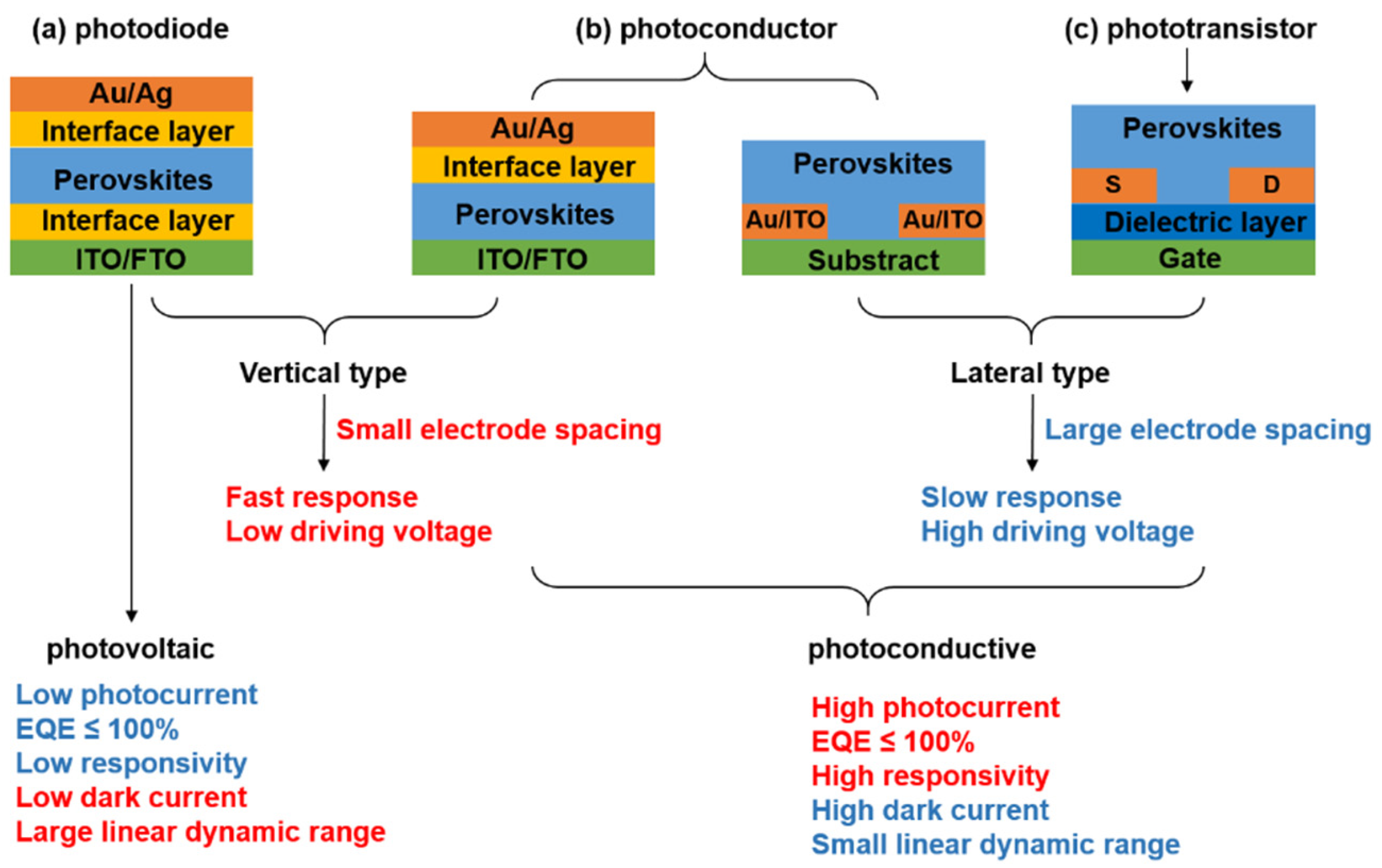
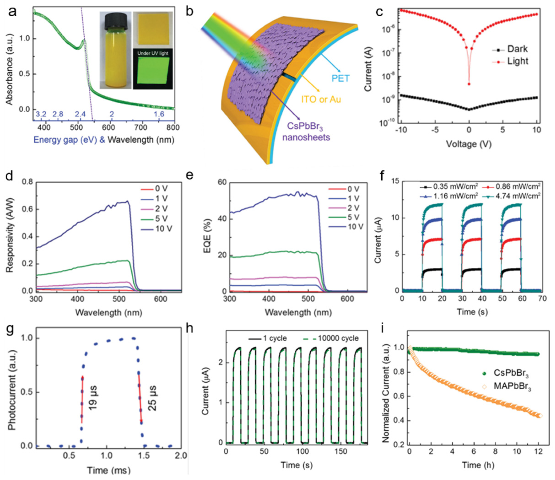
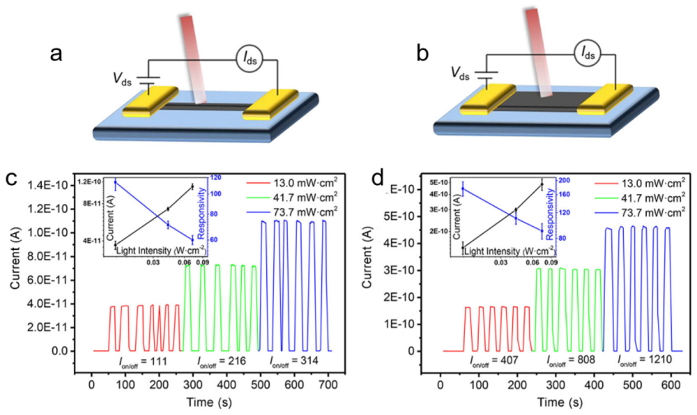
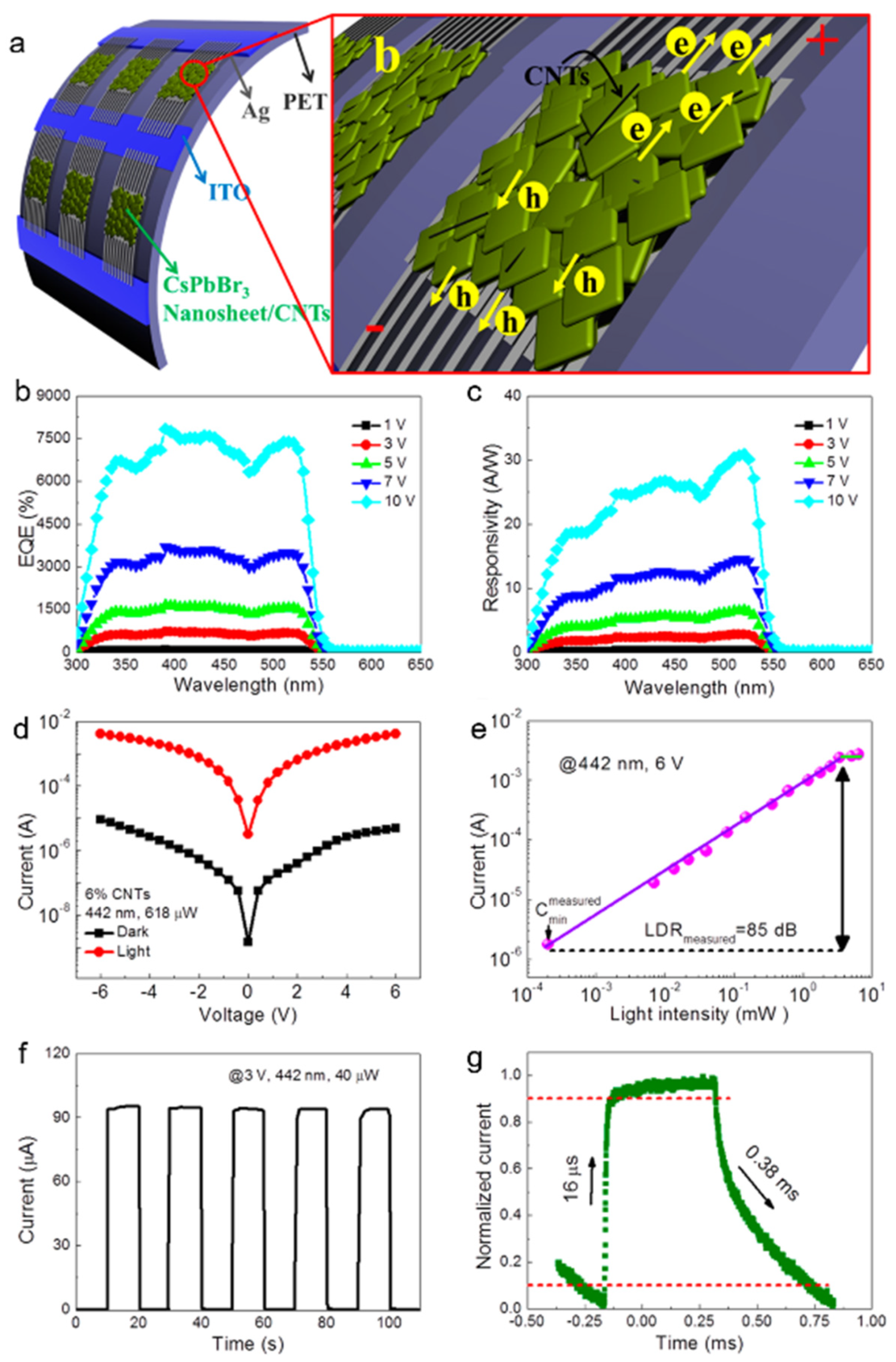
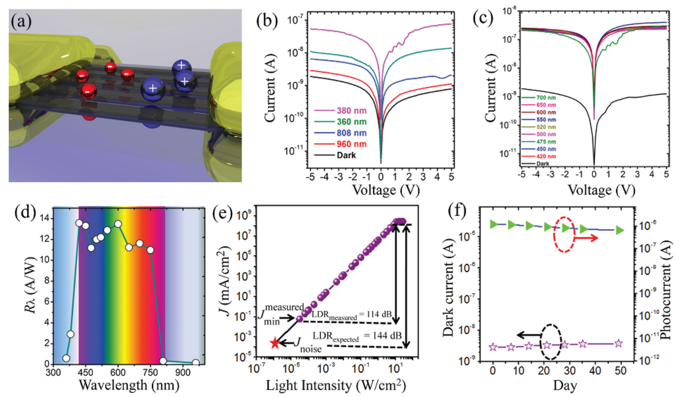
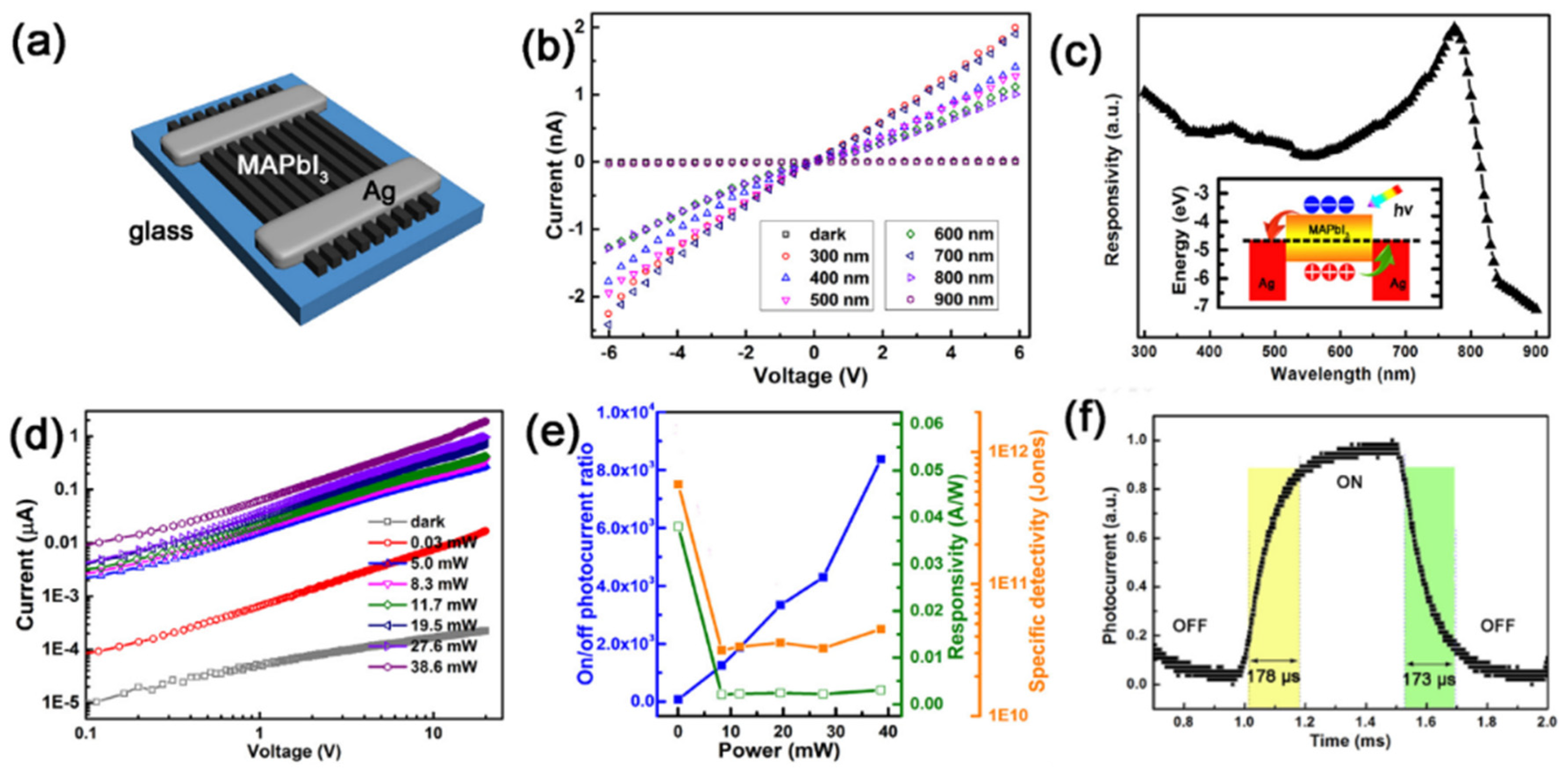
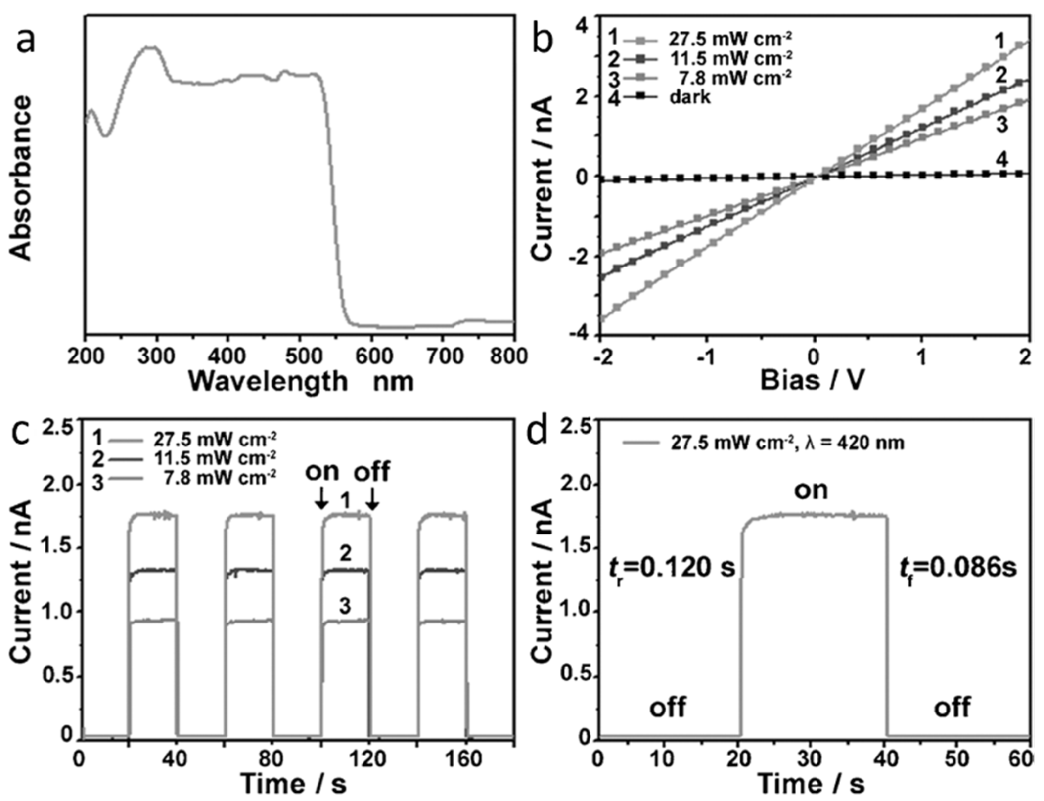
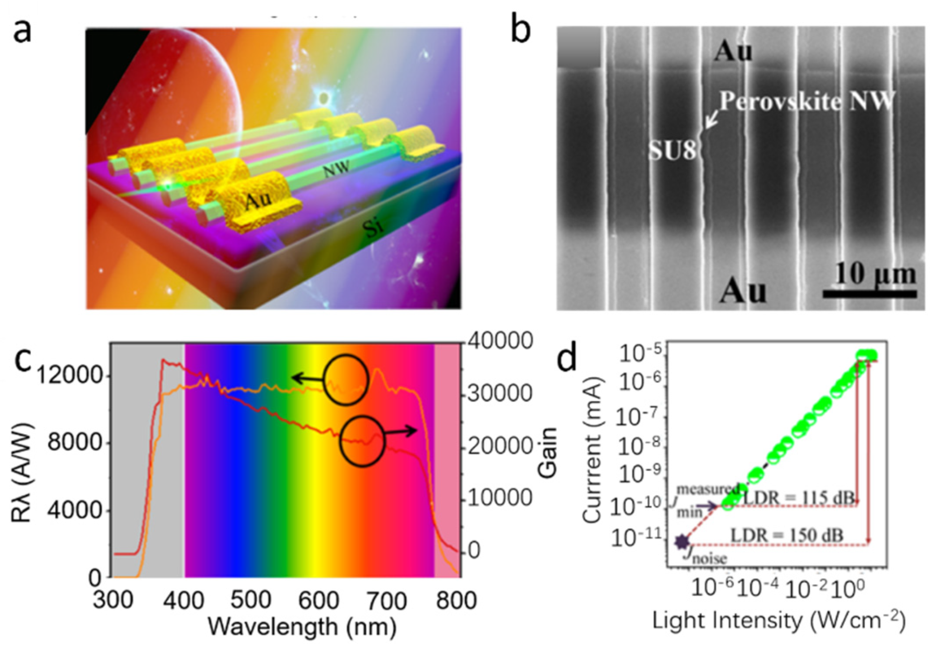
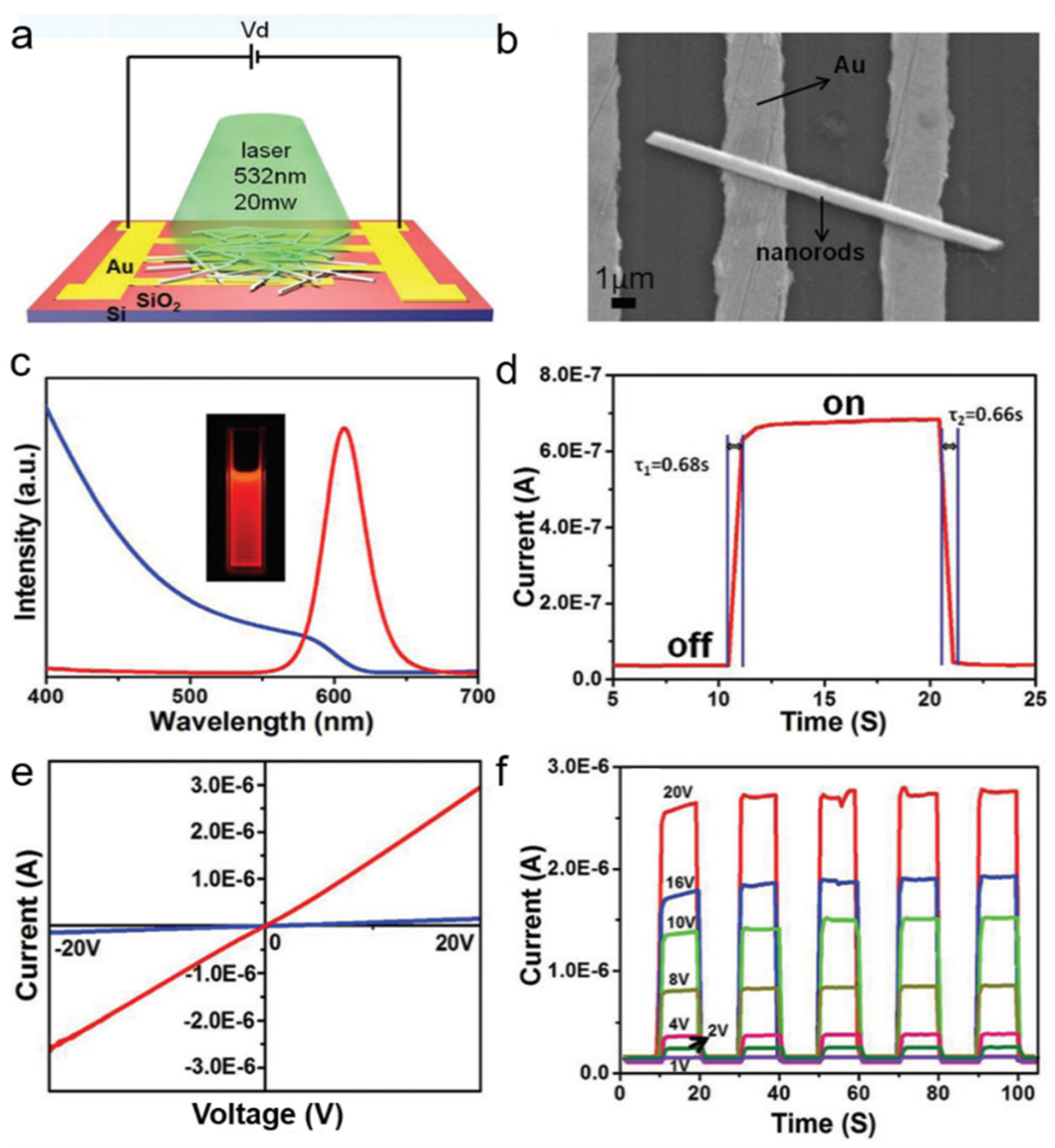
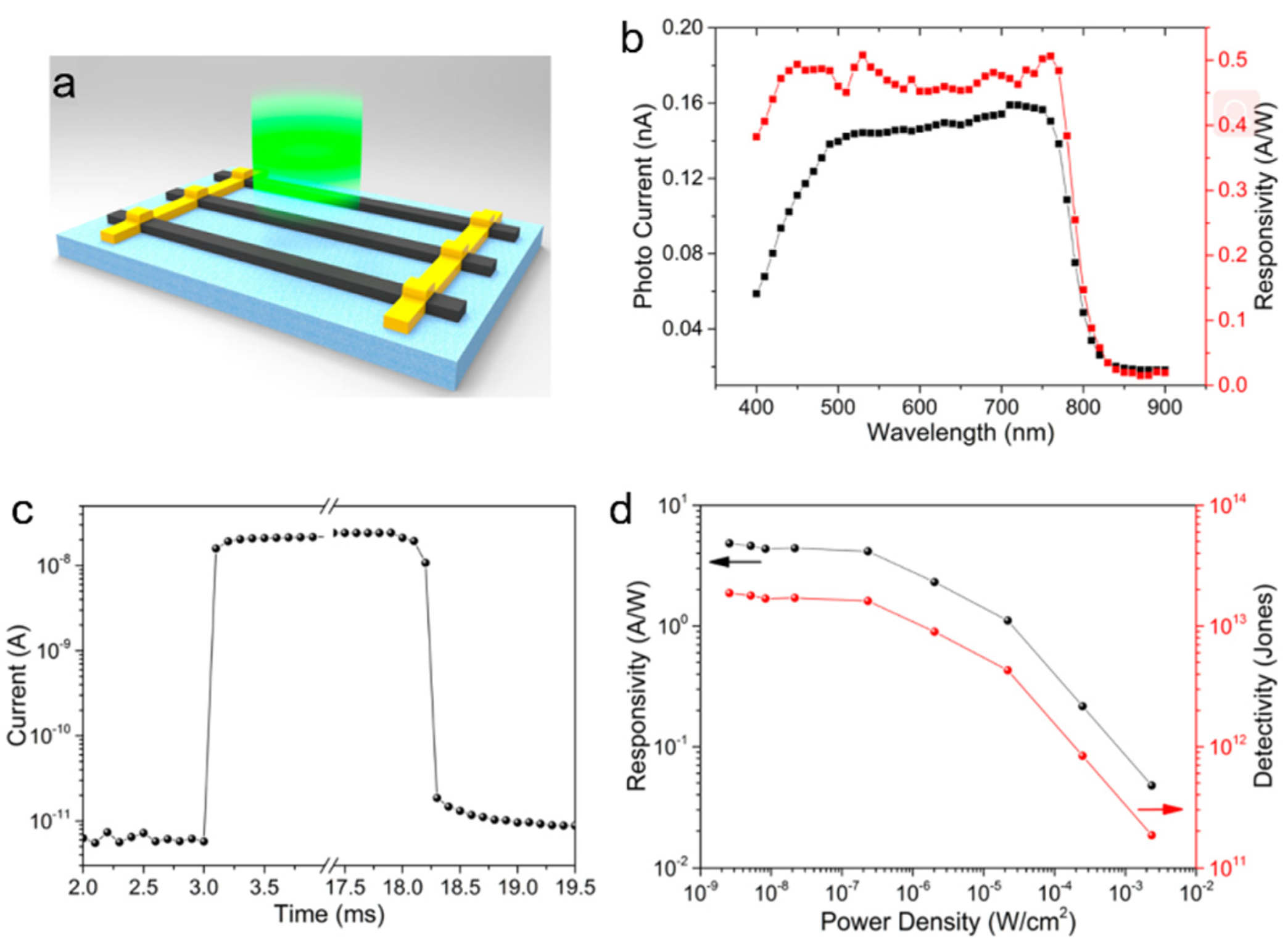
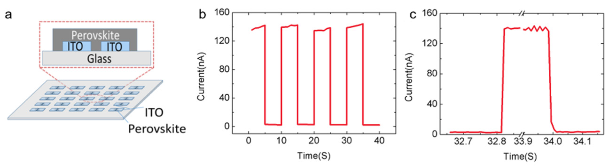
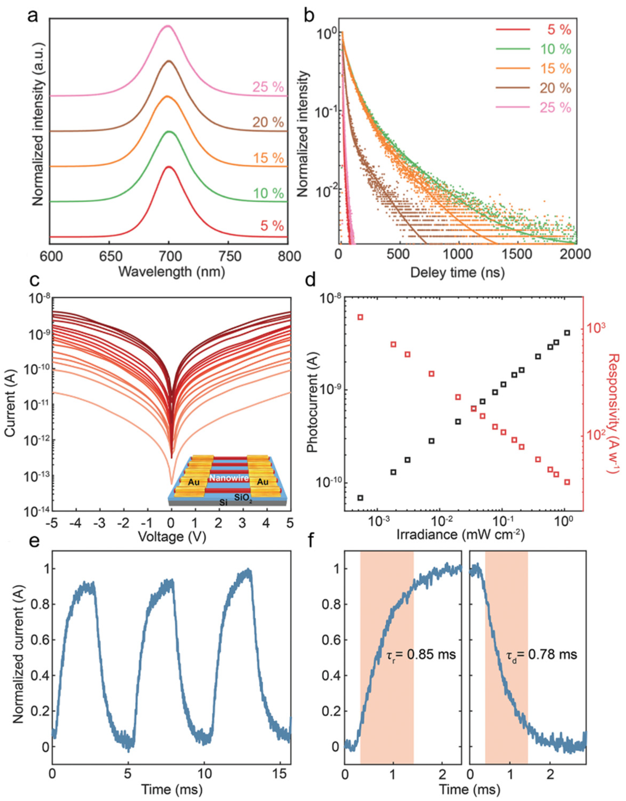
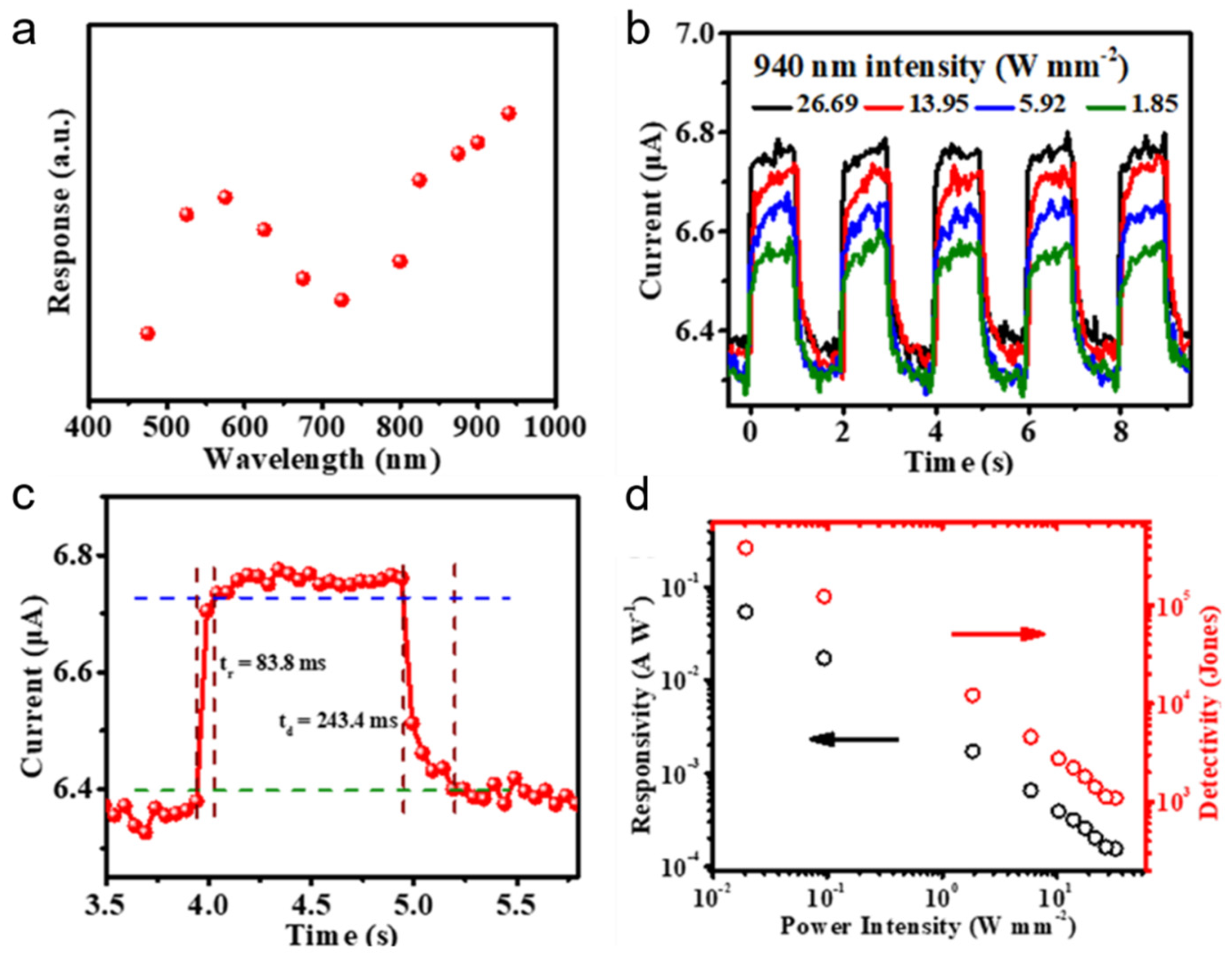
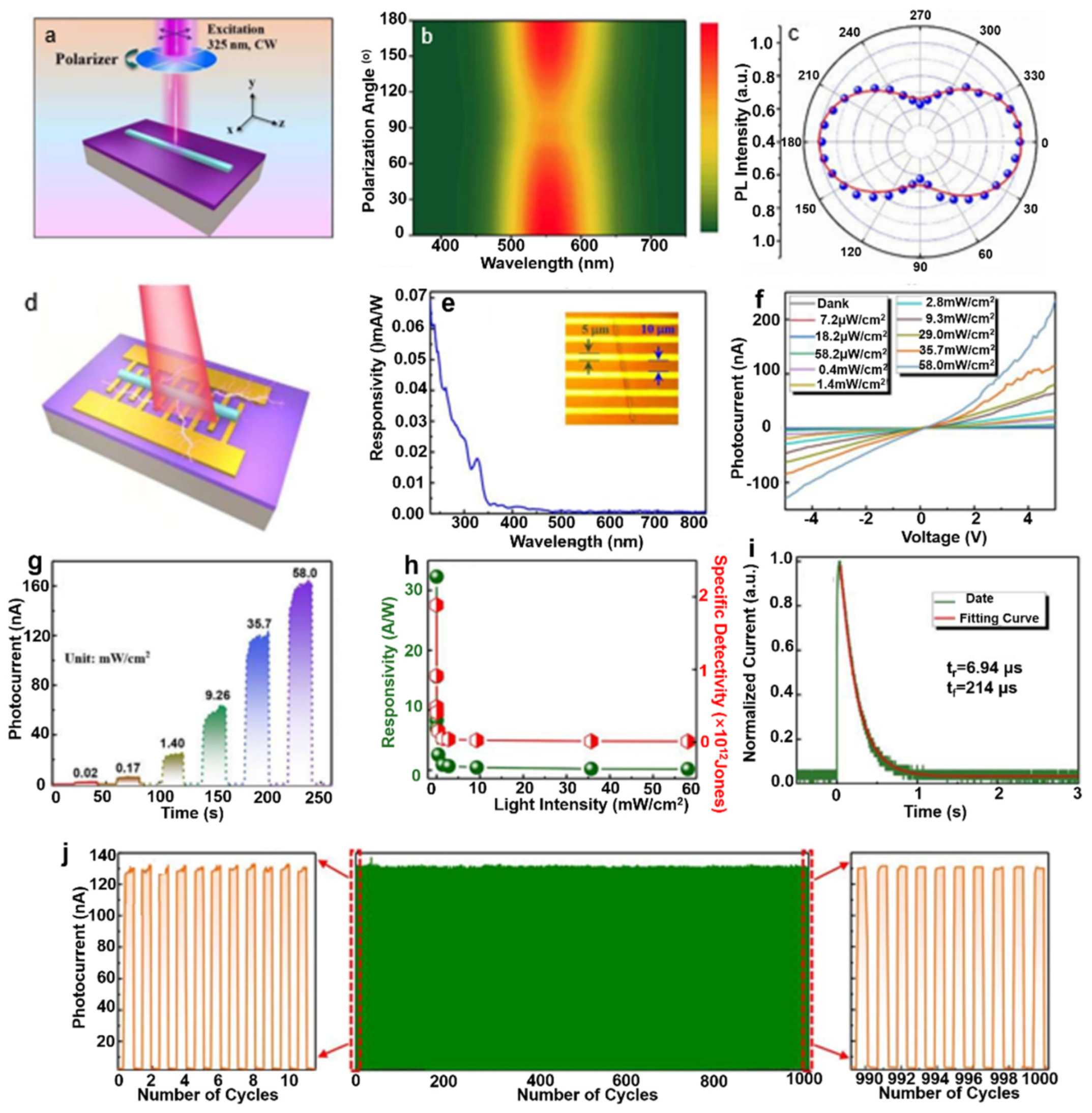
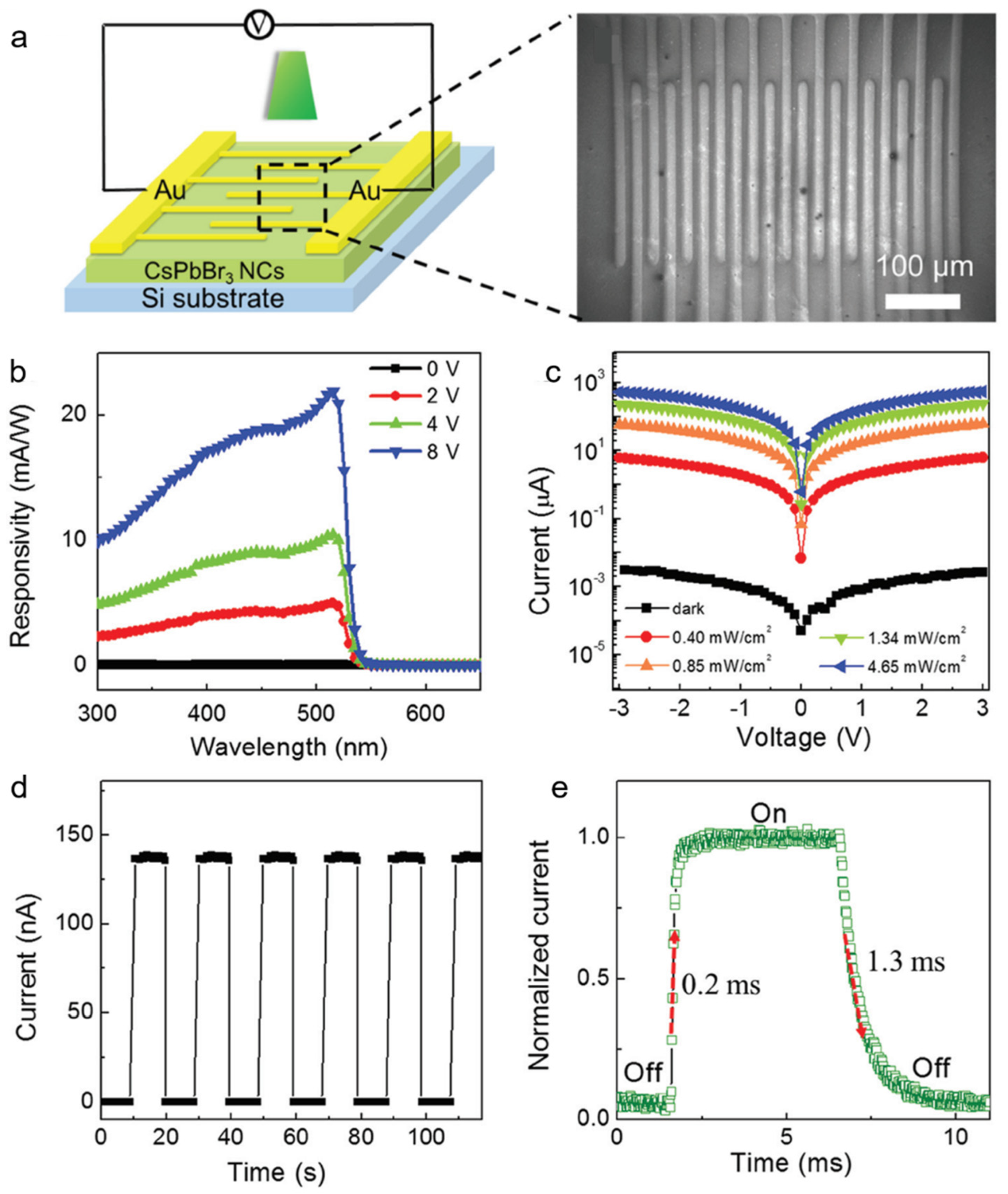
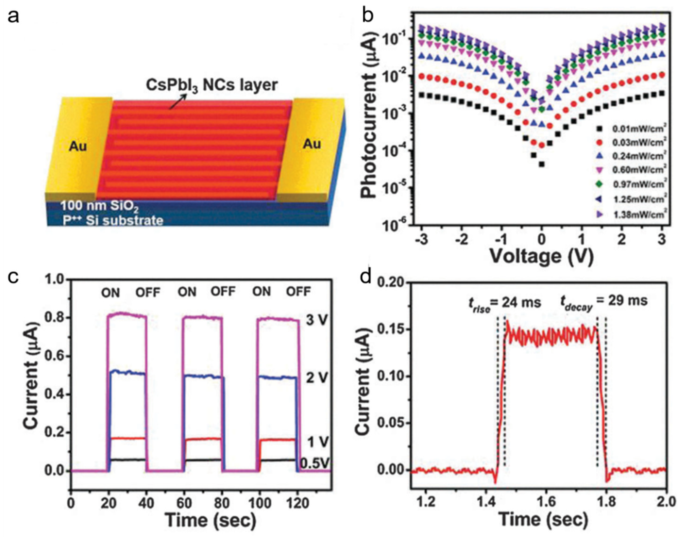
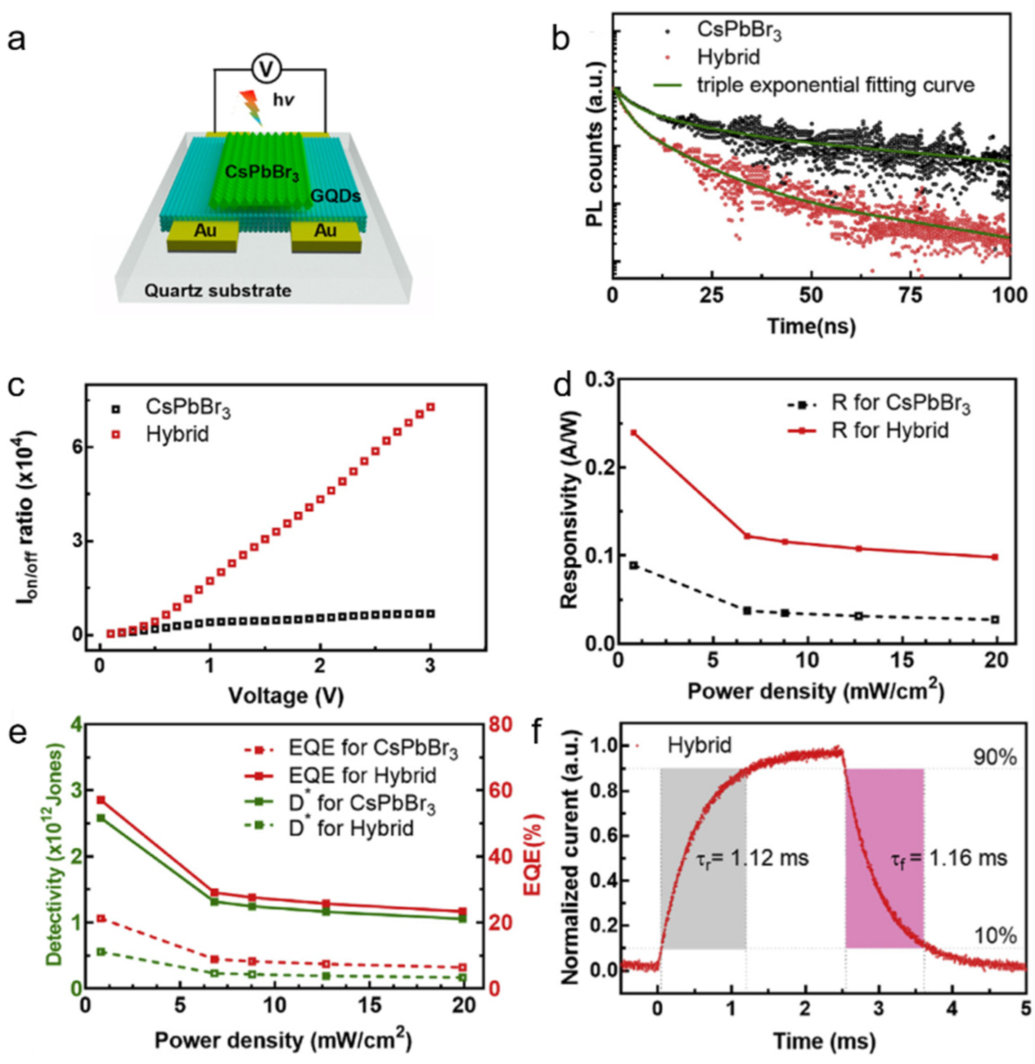
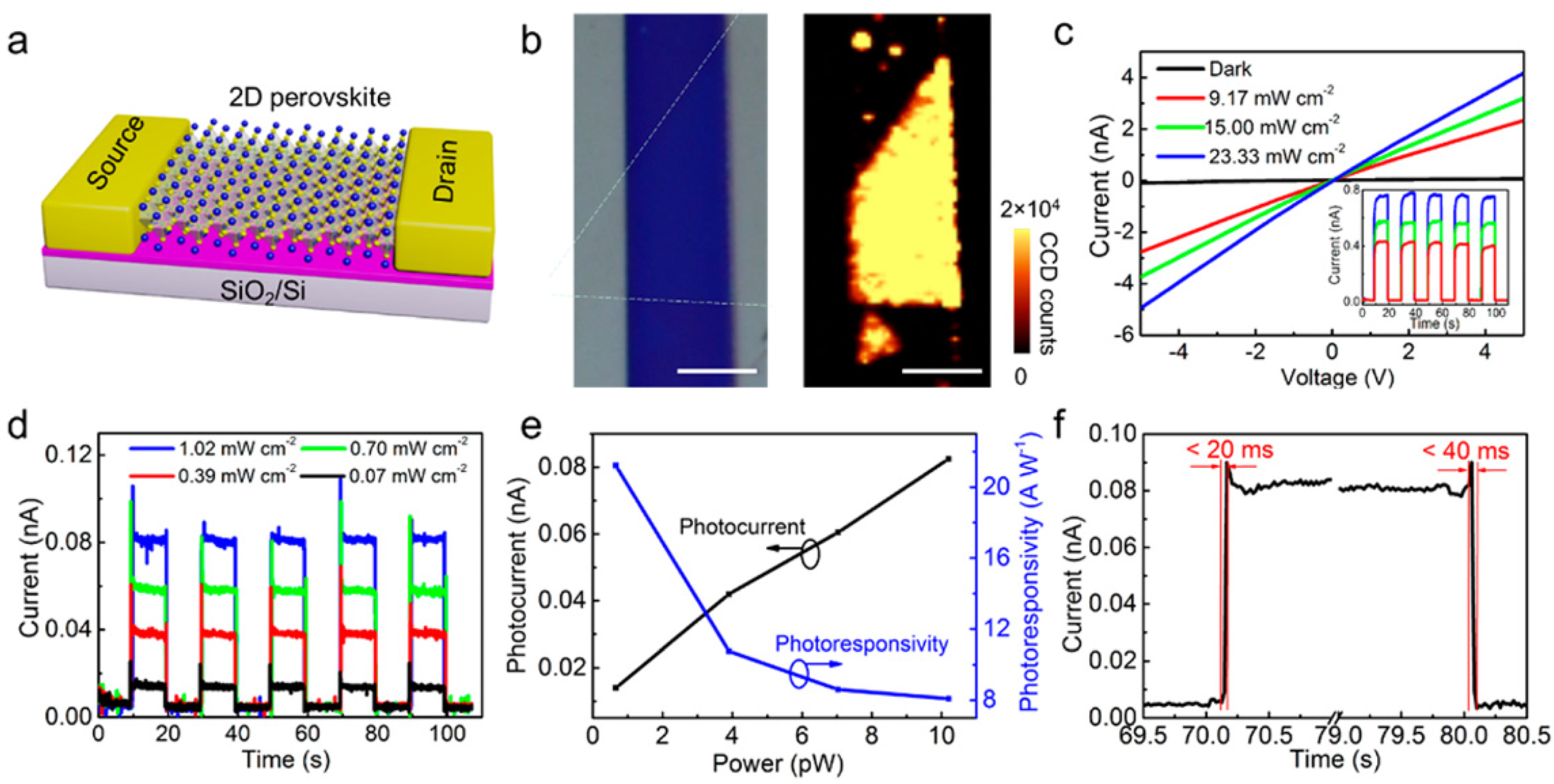
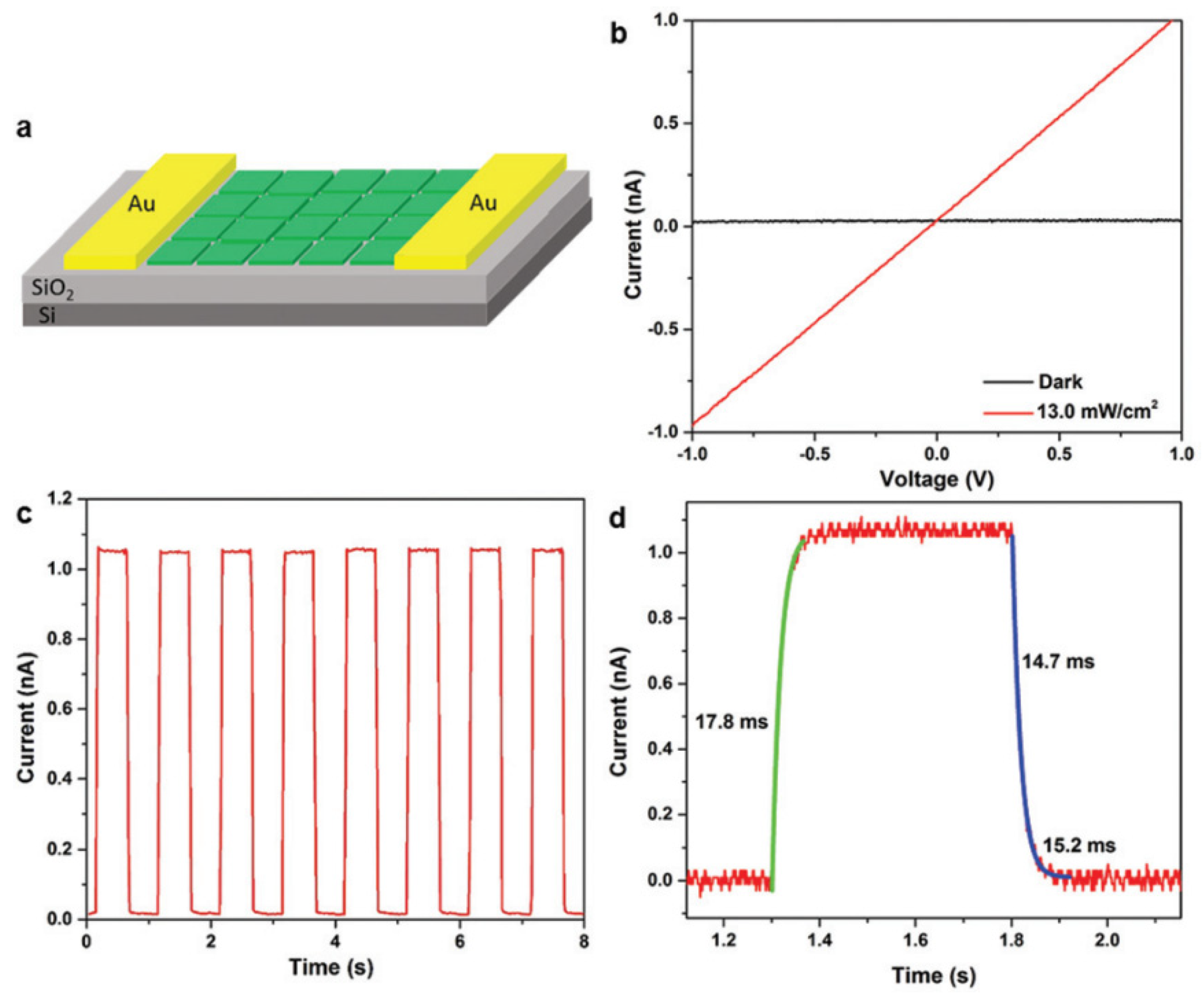
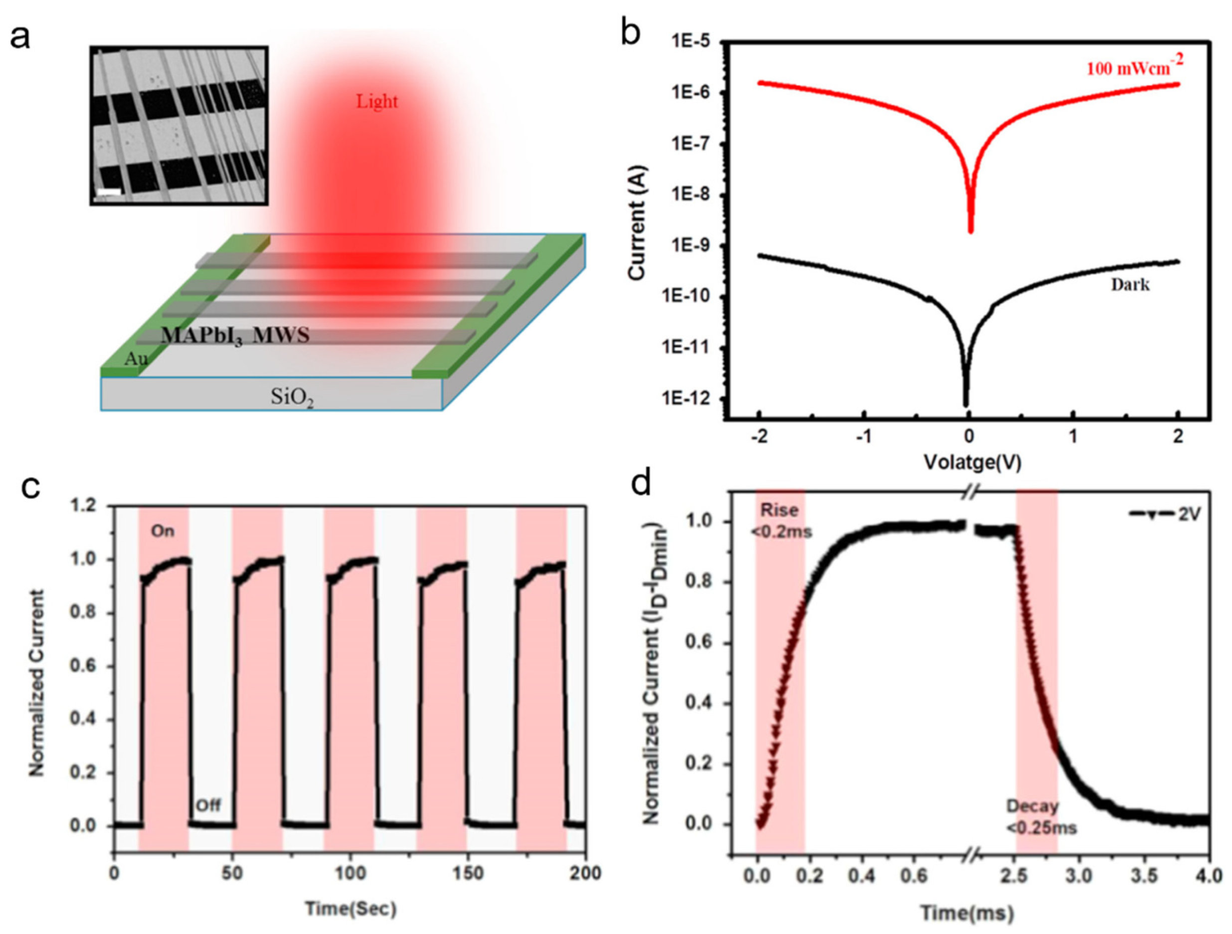
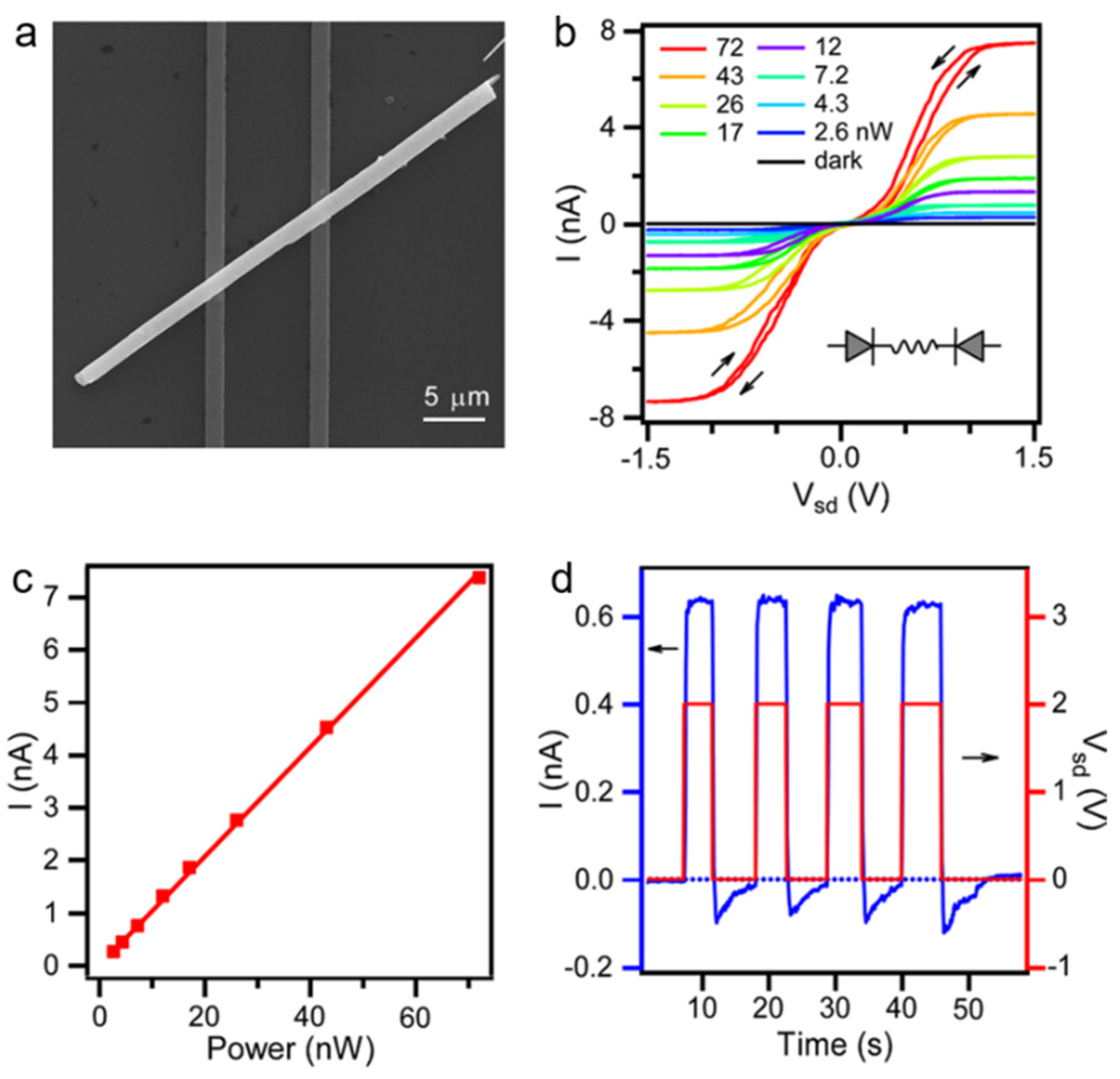
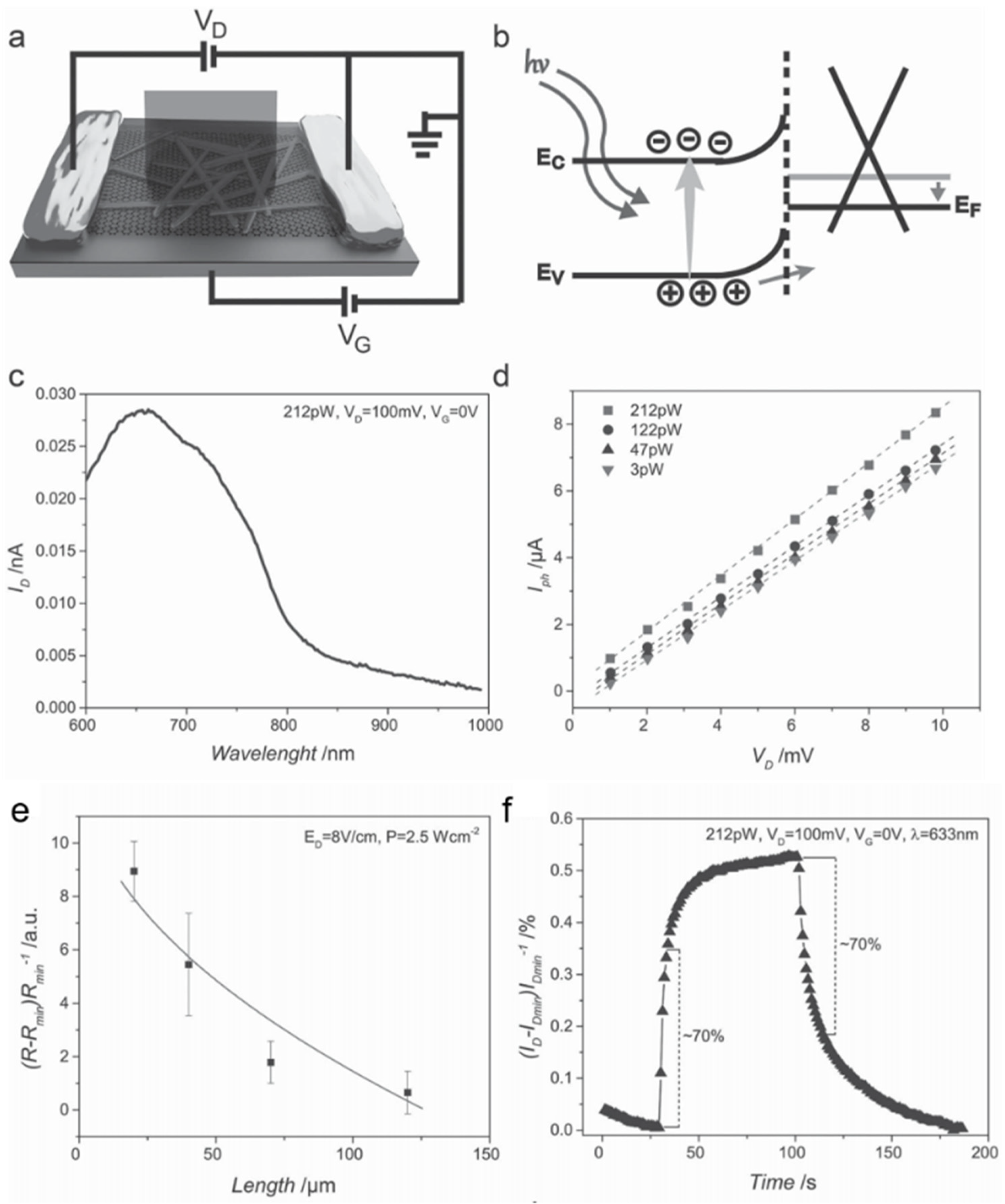
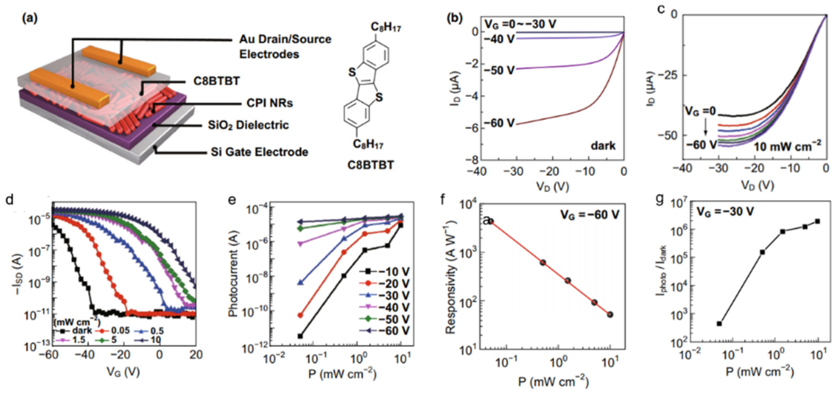
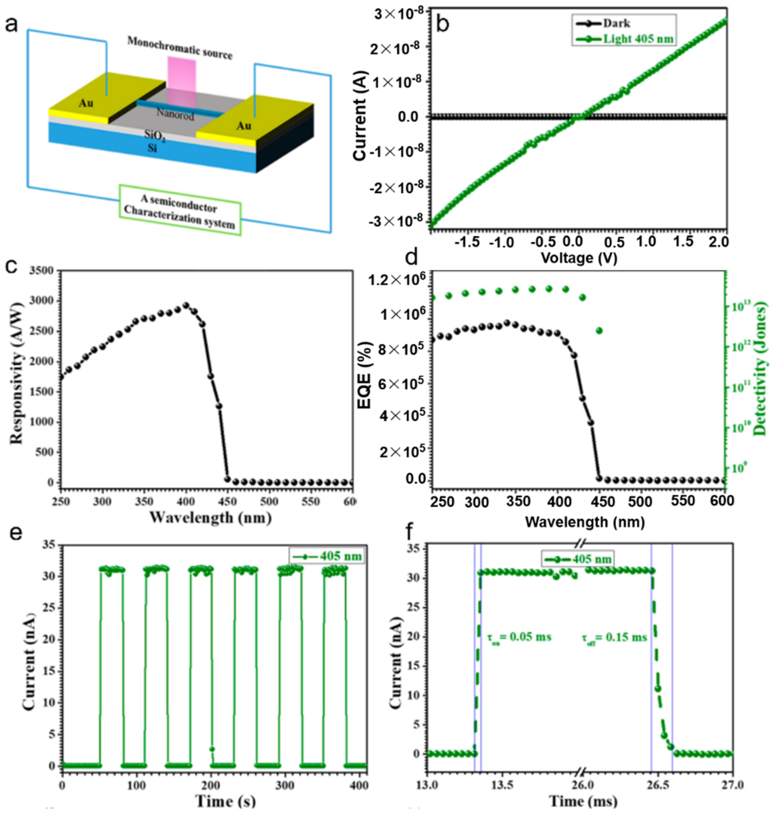
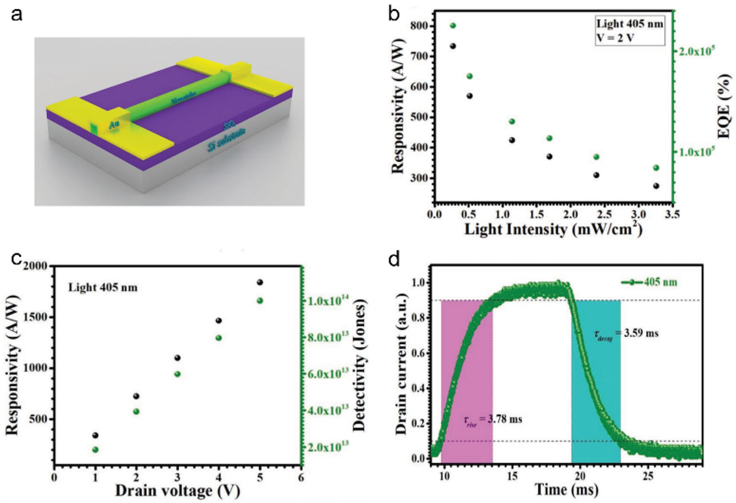
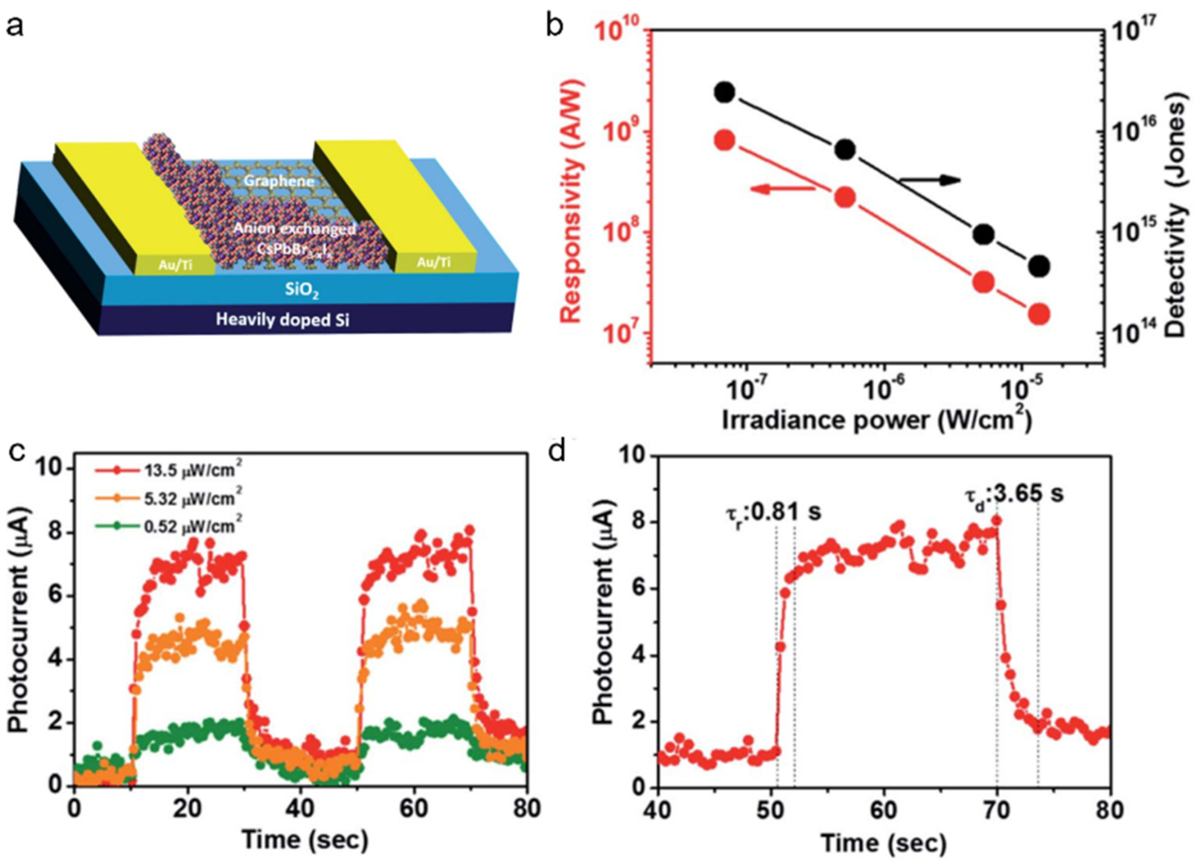
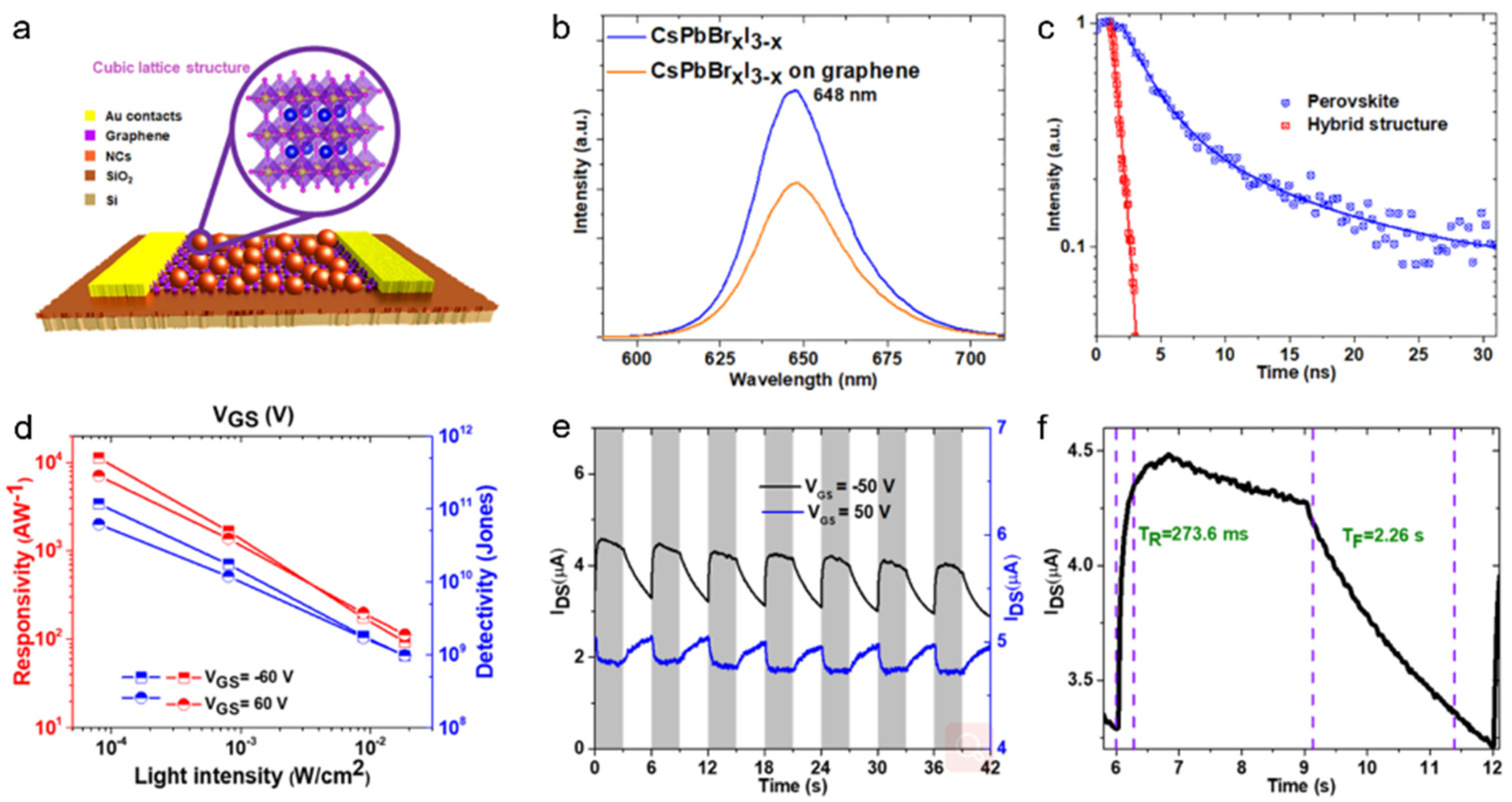
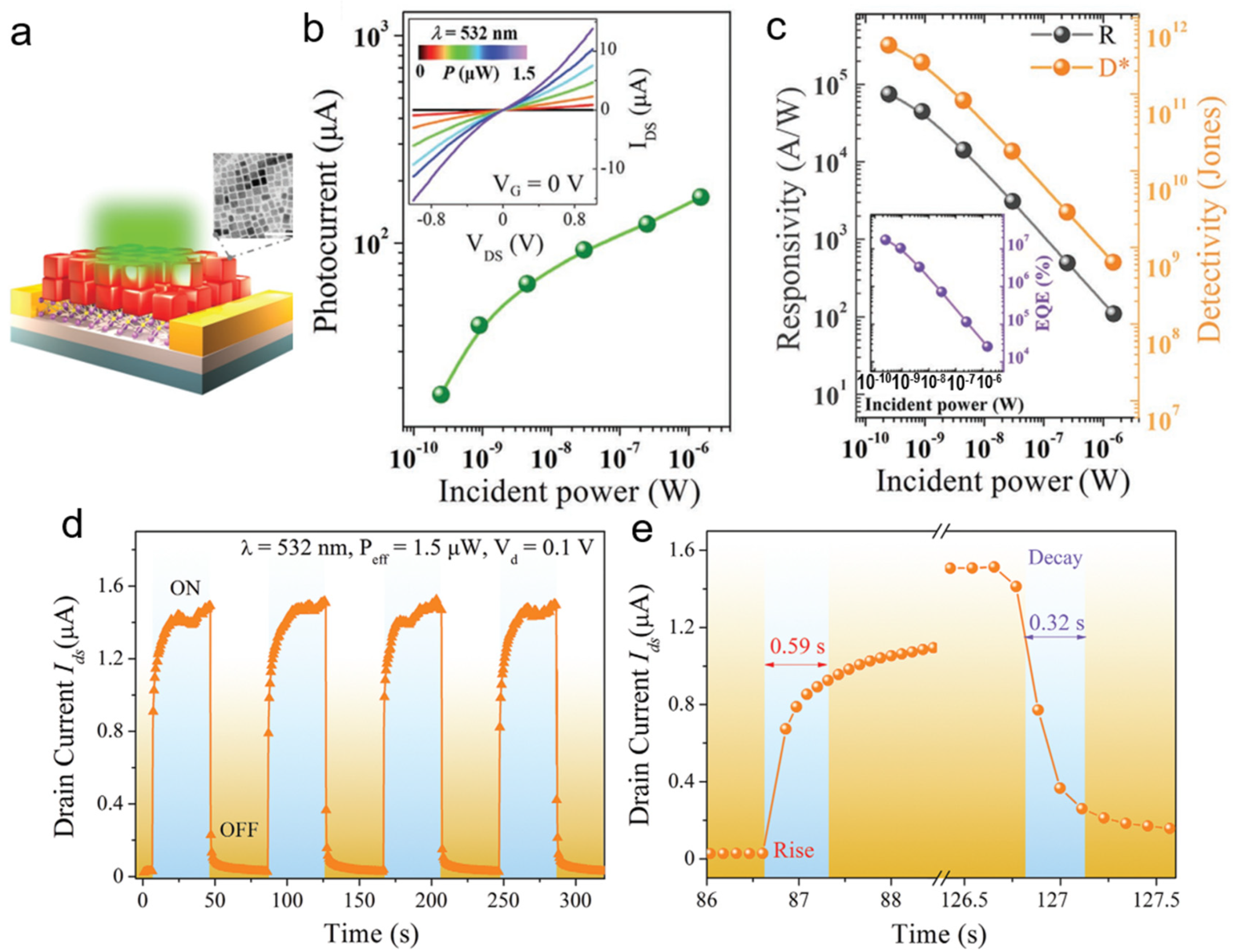
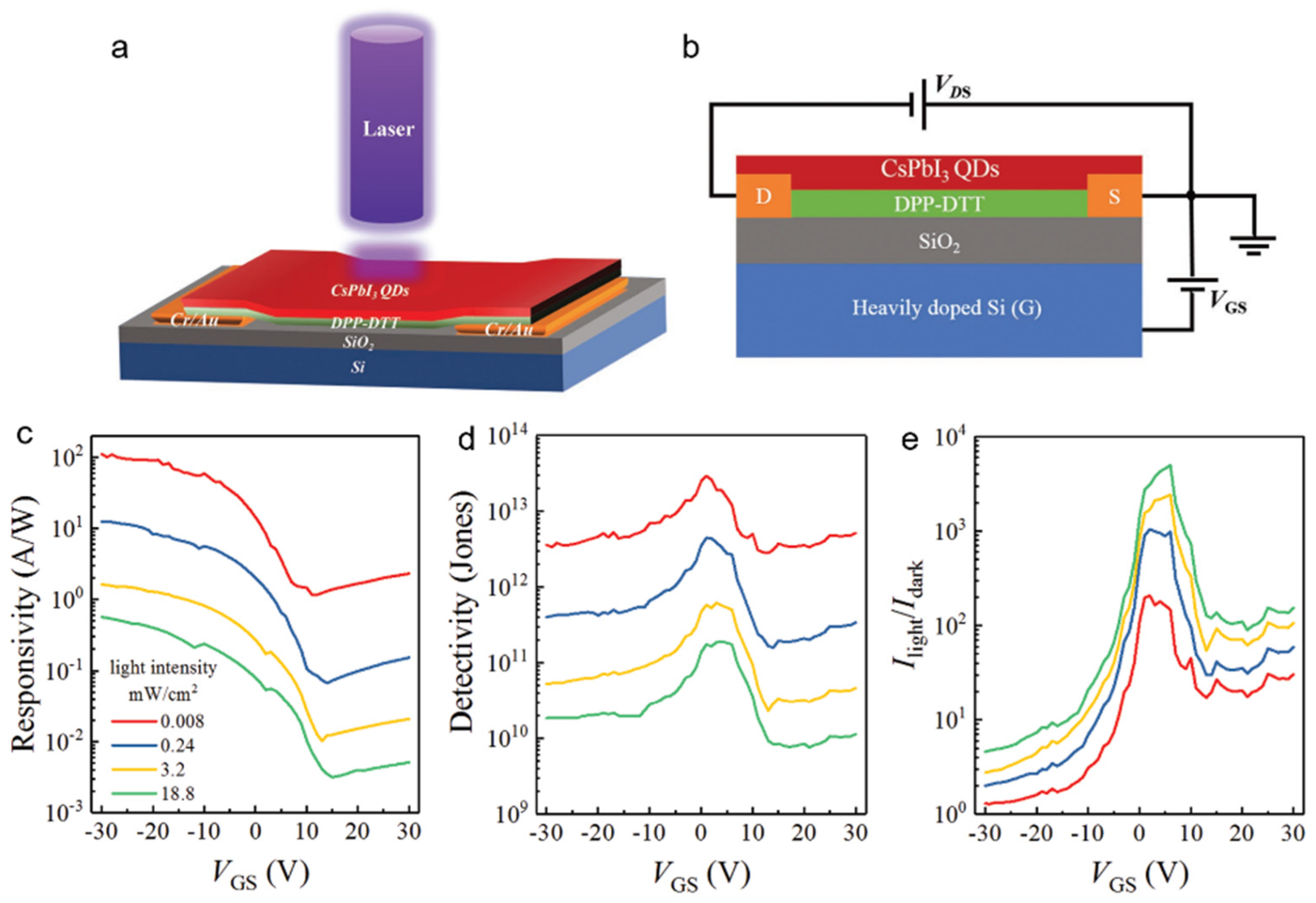
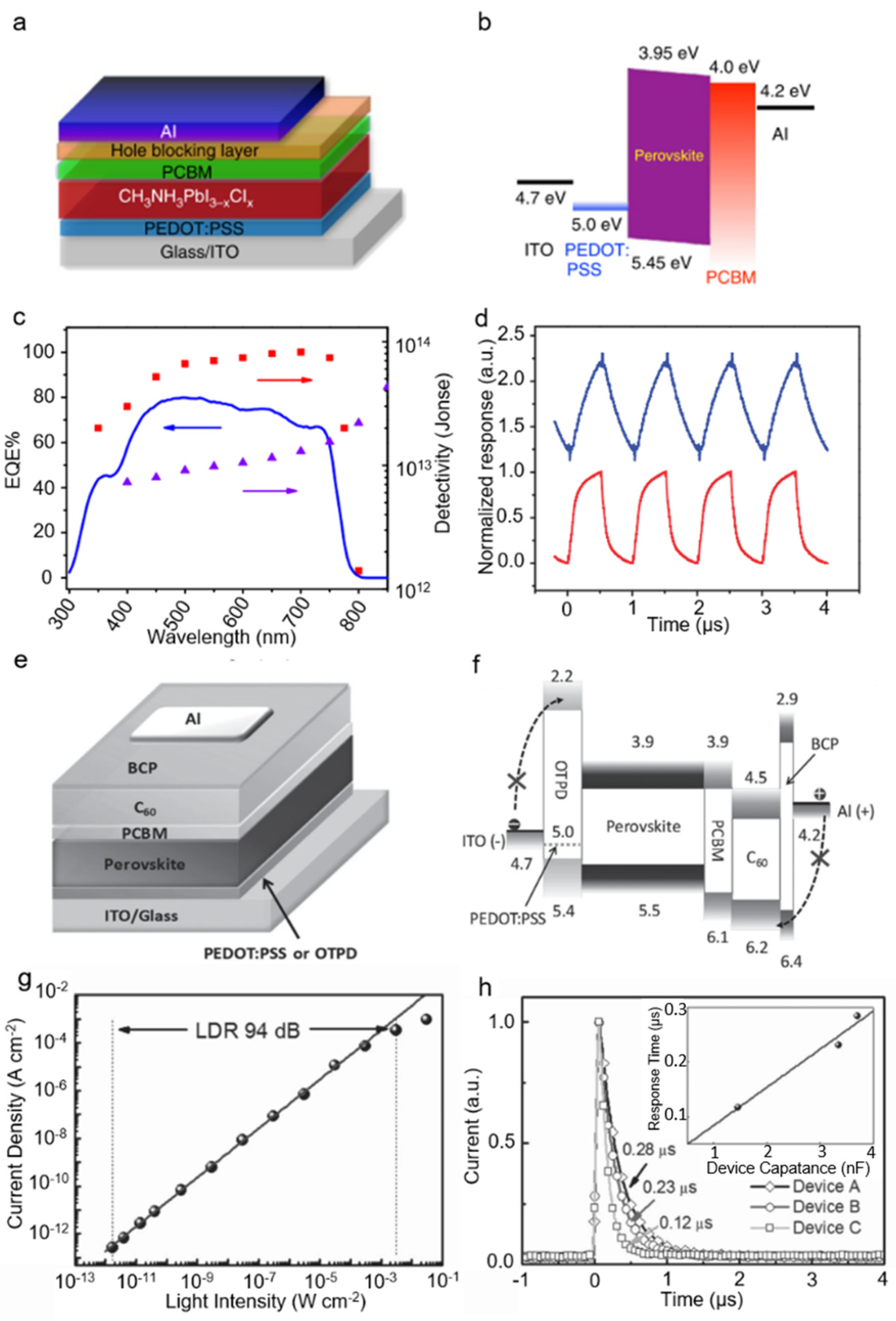
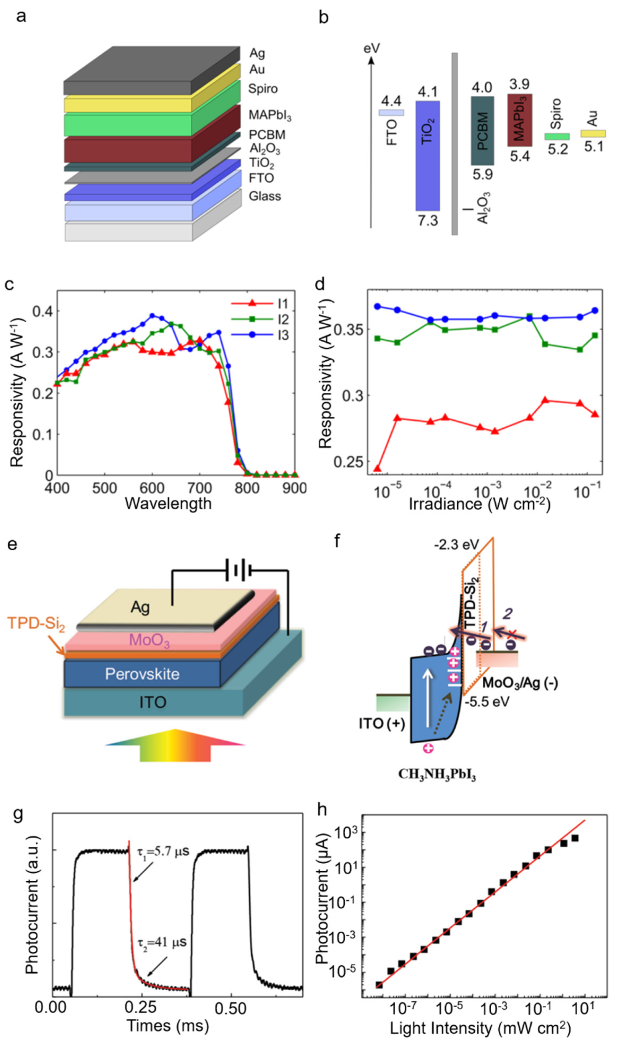
Table 1.
The key parameters of photodetectors.
| Parameters | Definition |
|---|---|
| Photoresponsivity (R) | the ratio of the photocurrent to the incident power on the active area: R = (Ip − Id)/(PA), where Ip is the photocurrent, Id is the dark current, P is the light intensity, A is the active area |
| EQE | Photoelectric conversion efficiency. EQE = Rhc/e, where h is the Planck’s constant, c is the light velocity, e is the electronic charge. |
| Gain (G) | The number of charge carriers through external circuit for per incident photon: G = τl/τt = τl(µV)/d2, where τl is the carrier lifetime, τt is the carrier transit time, µ is the carrier mobility, V is bias voltage, d is the channel length |
| Detectivity (D*) | D* = (A△ f)1/2/NEP, where A is the active area of the detector, △f is the electrical bandwidth, NEP is the noise equivalent power. |
| LDR | LDR usually stands for “Linear Dynamic Range”, defined as the range in which the current response of the photodetector is linearly proportional to the light intensity. LDR = 20 log (Ip*/Id), Where Id is the dark current. |
| Response speed (rise/decay time) | The ability of devices to track the incident light signal. |
Table 2.
Key characteristics of nanostructured perovskites-based photodetectors.
| Device | Dimension | Perovskite | R | D | EQE | On/Off Ratio | Gain | LDR | Rise/Decay Time | Ref |
|---|---|---|---|---|---|---|---|---|---|---|
| Photoconductor | 2D | CsPbBr3 | 0.25 | 53% | 19 µs/25 µs | [43] | ||||
| MAPbI3 | 1210 | [53] | ||||||||
| CsPbBr3/CNTs | 31.1 | 7488% | 16 µs/0.38 ms | [55] | ||||||
| 1D | MAPbI3 | 13.57 | 5.25 × 10¹² | [56] | ||||||
| MAPbI3 | 0.04 | 0.6 × 10¹² | 0.84 × 10⁴ | 178 µs/173 µs | [57] | |||||
| MAPbBr3 | 61.9 | 0.12 s/0.086 s | [58] | |||||||
| MAPb(I1-xBrx)3 | 1.25 × 10⁴ | 1.73 × 10¹¹ | 36,800 | 150 | [59] | |||||
| MAPb(I/Br)3 | 103 | 2000 | 0.68 s/0.66 s | [60] | ||||||
| MAPbI3 | 0.45 | 2 × 10¹³ | 4000 | <0.1 ms | [61] | |||||
| MAPbI3 | 1.2 | 2.39 × 10¹² | 160 | [62] | ||||||
| CsPbI3 | 1294 | 2.6 × 10¹⁴ | 0.85 ms/0.78 ms | [42] | ||||||
| CsSnI3 | 0.054 | 3.85 × 10⁵ | 83.8 ms/243.4 ms | [63] | ||||||
| CsCu2I3 | 32.3 | 1.89 × 10¹² | 2.6 × 10³ | 6.94 µs/214 µs | [64] | |||||
| others | CsPbBr3 | 0.0209 | 1.6 × 10⁵ | 0.2 ms/1.3 s | [65] | |||||
| CsPbX3 | 105 | 24 ms/29 ms | [52] | |||||||
| GQDs/CsPbBr3 | 0.24 | 2.5 × 10¹² | 57% | 7.2 × 10⁴ | 1.16 ms (Decay) | [66] | ||||
| Phototransistor | 2D | MAPbX3 | 22 | 1012 | 20 ms/40 ms | [67] | ||||
| CsPbBr3 | 17.8 ms/(14.7 ms/15.2 ms) | [68] | ||||||||
| 1D | MAPbI3 | 0.35 ms/0.25 ms | [69] | |||||||
| MAPbI3 | 0.3 | 4.02 × 10³ | 0.2 ms/0.25 ms | [70] | ||||||
| MAPbI3 | 0.11 | 0.25 | [71] | |||||||
| MAPbI3 | 2.6 × 10⁶ | 55 s/75 s | [72] | |||||||
| C8BTBT/CsPbI3 | 4.3 × 10³ | 2.2 × 1066 | [73] | |||||||
| CsPbX3 | 4489 | 7.9 × 10¹² | <50 ms | [74] | ||||||
| CsPbI3 | 2.92 × 10³ | 5.17 × 10¹³ | 0.6 × 10⁶% | 50ms | [75] | |||||
| CsPbI3 | 1.84 × 10³ | 9.9 × 10¹³ | 5.65 × 10⁵% | 3.78 ms/539 ms | [76] | |||||
| others | Graphene/CsPbBr3-xIx | 8.2 × 10⁸ | 2.4 × 10¹⁶ | 0.81 s/3.65 s | [77] | |||||
| Graphene/CsPbBrxI3-x | 1.12 × 10⁵ | 1.17 × 10¹¹ | 9.32 × 10¹⁰ | 273.6 ms/2.26 s | [78] | |||||
| CsPbI3-xBrx | 7.7 × 10⁴ | 5.6 × 10¹¹ | 107% | 0.59 s/0.32 s | [44] | |||||
| CsPbI3/DPP-DTT | 110 | 2.9 × 10¹³ | 6 × 10³ | [79] |
Publisher’s Note: MDPI stays neutral with regard to jurisdictional claims in published maps and institutional affiliations. |
© 2021 by the authors. Licensee MDPI, Basel, Switzerland. This article is an open access article distributed under the terms and conditions of the Creative Commons Attribution (CC BY) license (https://creativecommons.org/licenses/by/4.0/).
Share and Cite
MDPI and ACS Style
Li, C.; Li, J.; Li, Z.; Zhang, H.; Dang, Y.; Kong, F. High-Performance Photodetectors Based on Nanostructured Perovskites. Nanomaterials 2021, 11, 1038. https://doi.org/10.3390/nano11041038
AMA Style
Li C, Li J, Li Z, Zhang H, Dang Y, Kong F. High-Performance Photodetectors Based on Nanostructured Perovskites. Nanomaterials. 2021; 11(4):1038. https://doi.org/10.3390/nano11041038
Chicago/Turabian StyleLi, Chunlong, Jie Li, Zhengping Li, Huayong Zhang, Yangyang Dang, and Fangong Kong. 2021. "High-Performance Photodetectors Based on Nanostructured Perovskites" Nanomaterials 11, no. 4: 1038. https://doi.org/10.3390/nano11041038
Note that from the first issue of 2016, this journal uses article numbers instead of page numbers. See further details here.