Graphene Templated DNA Arrays and Biotin-Streptavidin Sensitive Bio-Transistors Patterned by Dynamic Self-Assembly of Polymeric Films Confined within a Roll-on-Plate Geometry

 and
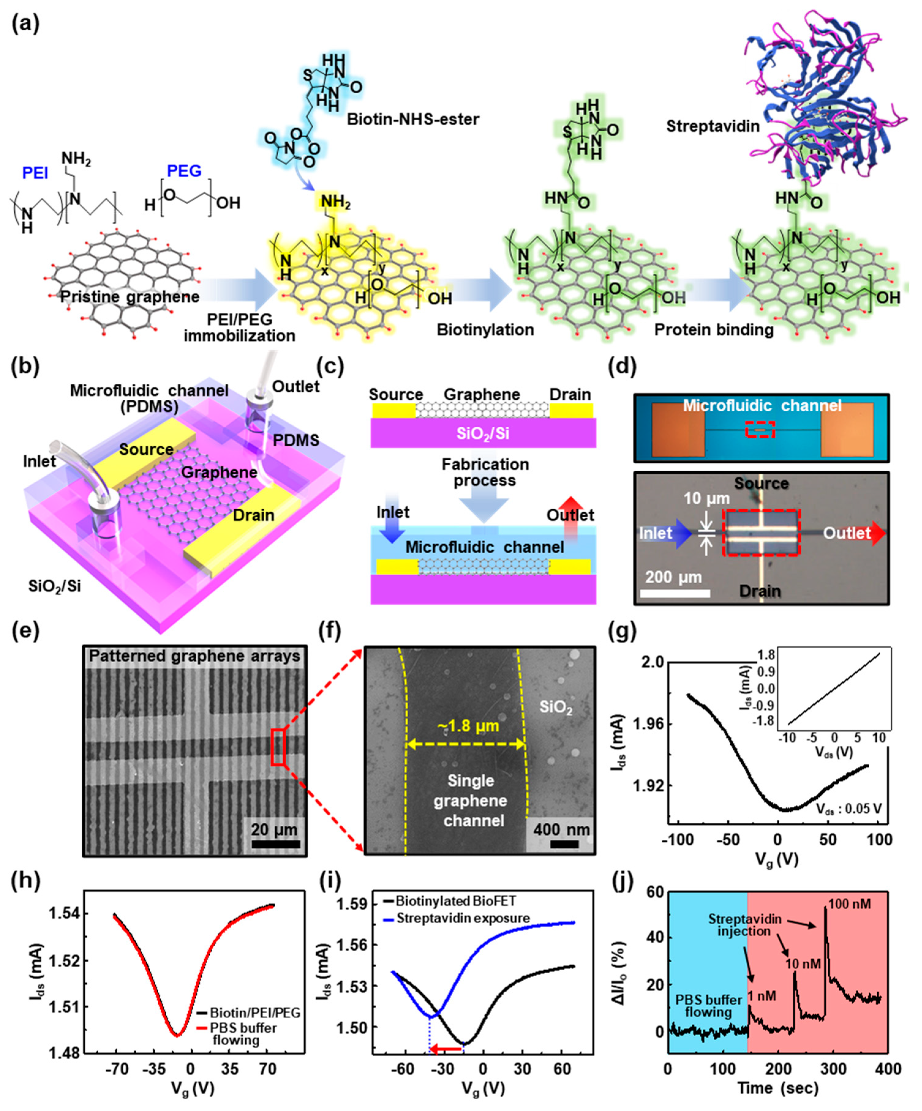
and 
Abstract
:1. Introduction
2. Materials and Methods
2.1. Roll-on-Plate Confined Geometry
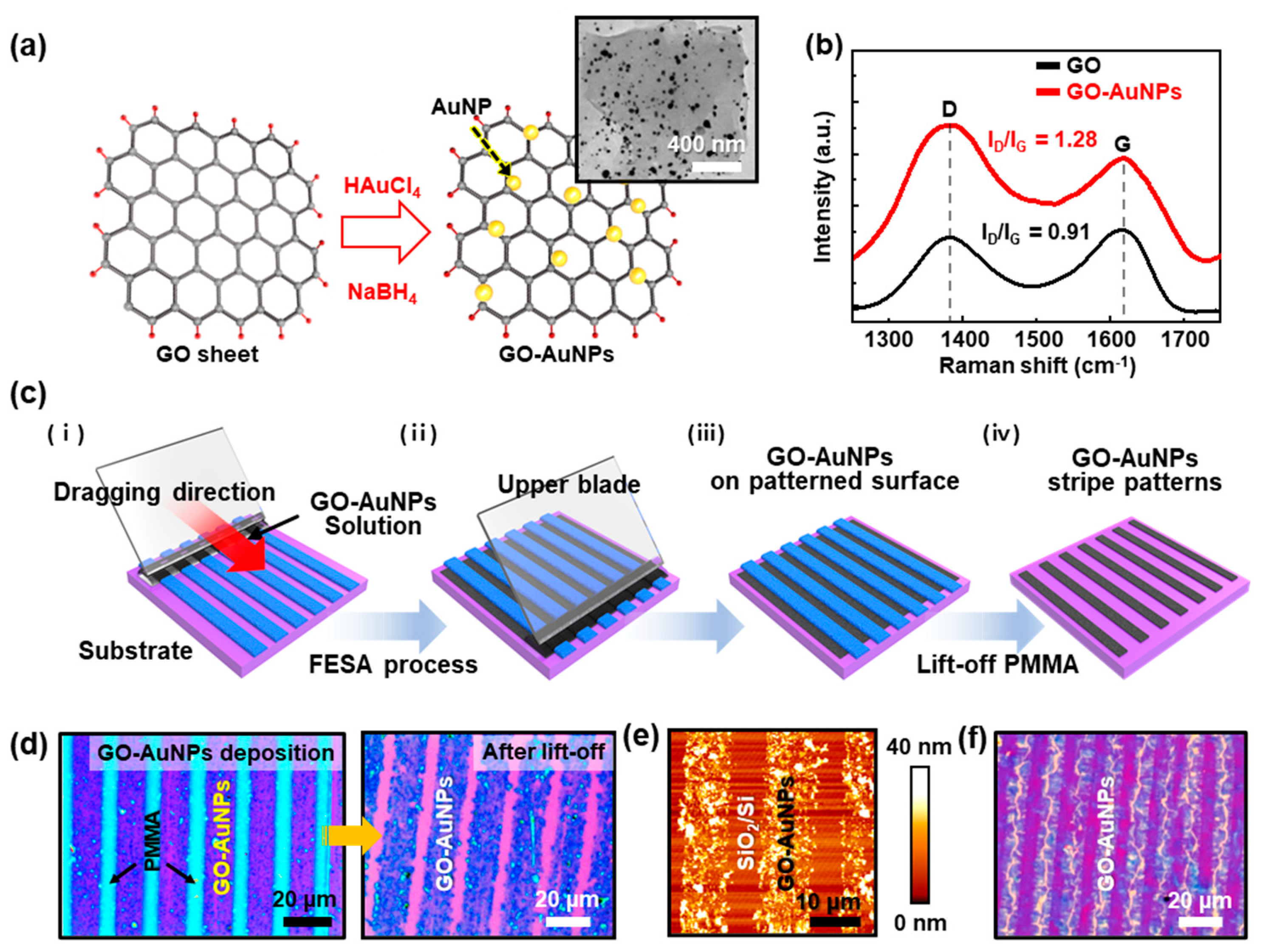
2.2. Synthesis of the Au Nanoparticles Decorated Graphene Oxide (GO/AuNPs)
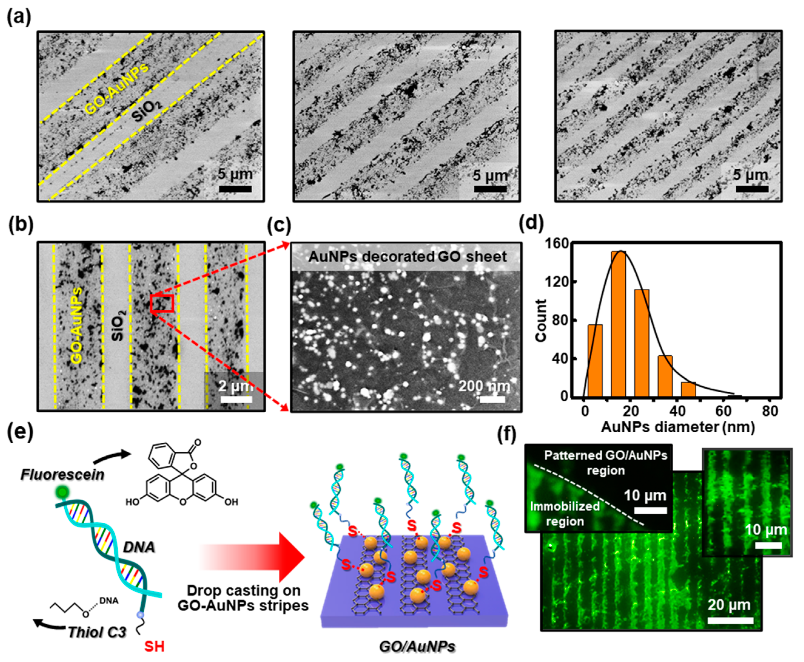
2.3. Fabrication of GO/AuNPs Patterns and DNA Immobilization
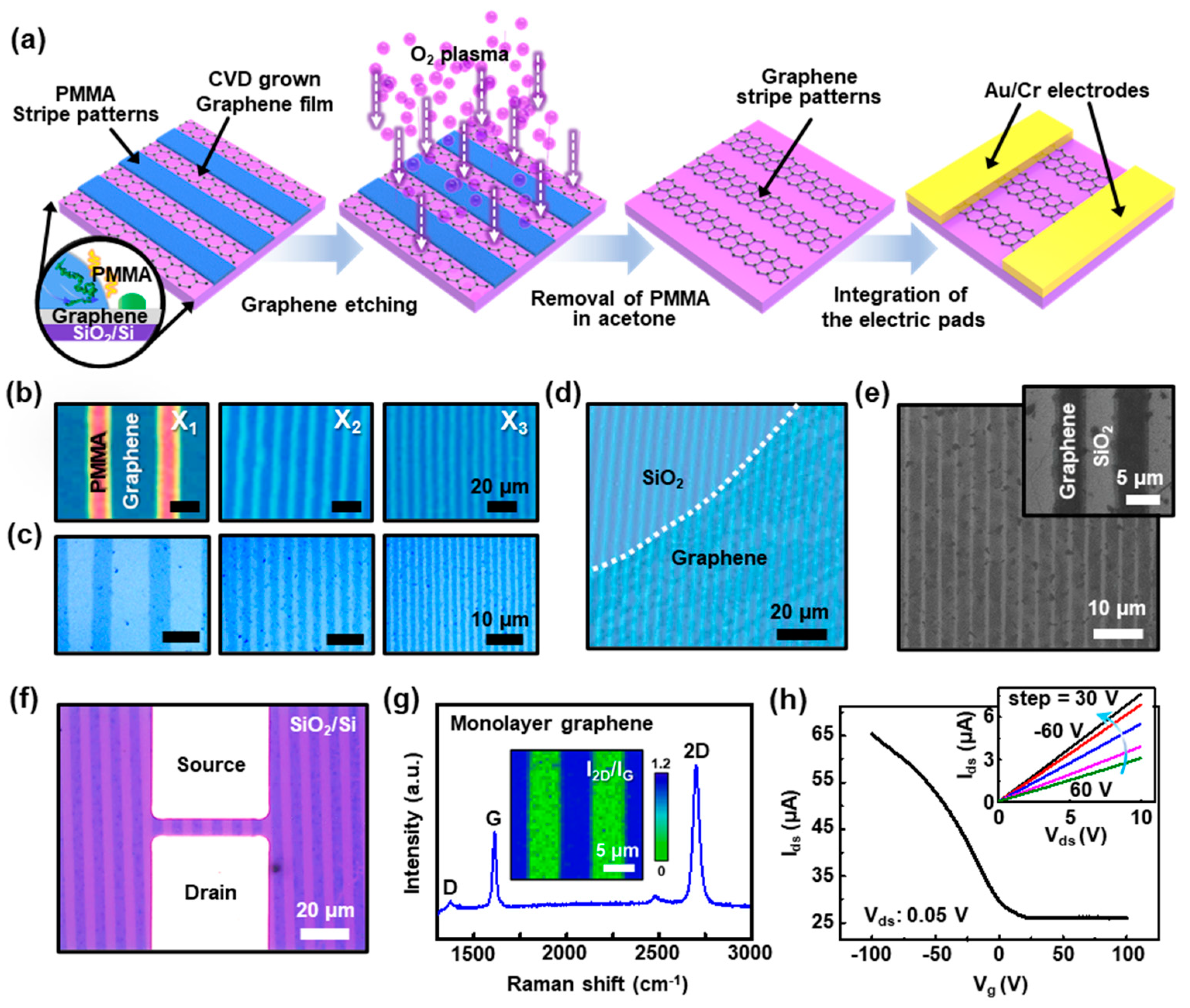
2.4. Synthesis of Monolayer Graphene
2.5. Fabrication of Microfluidic Channel
2.6. Graphene Surface Modification: Biotinylation and Streptavidin Detection
2.7. Characterization and Measurements
3. Results and Discussion
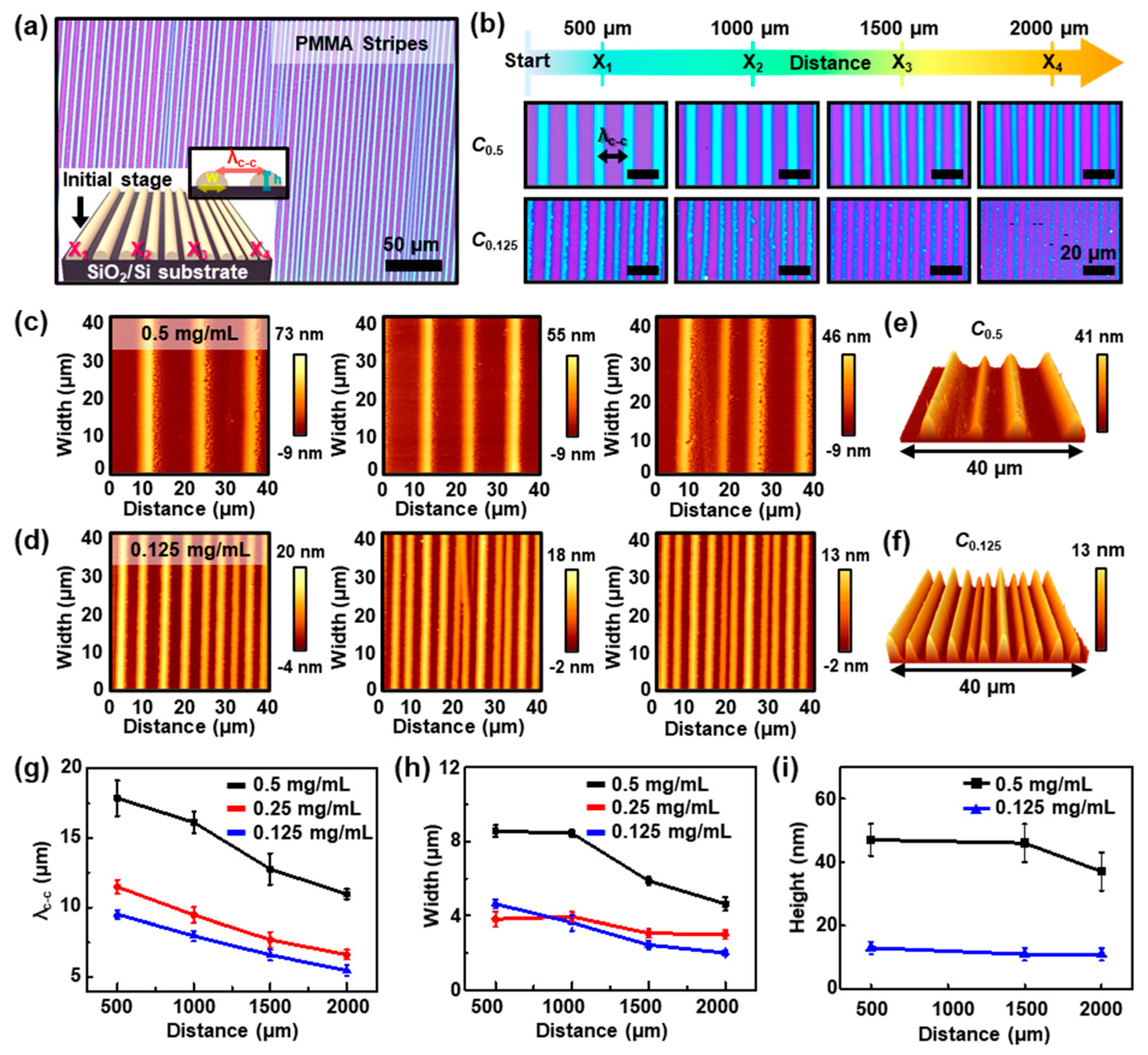
3.1. Evaporative Self-Assembly of PMMA Microstructures in Roll-to-Plate Geometry
3.2. Concentration Effect on the PMMA Pattern Formation
3.3. Template-Assisted Formation of GO/AuNPs Stripe Patterns
3.4. Selective Immobilization of Fluorescein-Labeled DNAs on the Patterned GO/AuNPs
3.5. PMMA Stripes as Etch Masks for the Aligned Arrays of CVD Grown Graphene Sheets
3.6. Graphene-Based BioGFETs for Biotin-Streptavidin Real-time Detection
4. Conclusions
Supplementary Materials
Author Contributions
Funding
Conflicts of Interest
References
- Birkholz, O.; Burns, J.R.; Richter, C.P.; Psathaki, O.E.; Howorka, S.; Piehler, J. Multi-functional DNA nanostructures that puncture and remodel lipid membranes into hybrid materials. Nat. Commun. 2018, 9, 1521. [Google Scholar] [CrossRef] [PubMed]
- Liu, Q.; Wu, C.; Cai, H.; Hu, N.; Zhou, J.; Wang, P. Cell-based biosensors and their application in biomedicine. Chem. Rev. 2014, 114, 6423–6461. [Google Scholar] [CrossRef] [PubMed]
- Grazon, C.; Baer, R.C.; Kuzmanovic, U.; Nguyen, T.; Chen, M.; Zamani, M.; Chern, M.; Arquino, P.; Zhang, X.; Lecommandoux, S.; et al. A progesterone biosensor derived from microbial screening. Nat. Commun. 2020, 11, 1276. [Google Scholar] [CrossRef] [PubMed] [Green Version]
- Li, H.; Liu, X.; Li, L.; Mu, X.; Genov, R.; Mason, A.J. CMOS electrochemical instrumentation for biosensor microsystems: A review. Sensors 2016, 17, 74. [Google Scholar] [CrossRef] [PubMed]
- Panwar, N.; Soehartono, A.M.; Chan, K.K.; Zeng, S.; Xu, G.; Qu, J.; Coquet, P.; Yong, K.T.; Chen, X. Nanocarbons for biology and medicine: Sensing, imaging, and drug delivery. Chem. Rev. 2019, 119, 9559–9656. [Google Scholar] [CrossRef] [PubMed]
- Maduraiveeran, G.; Sasidharan, M.; Ganesan, V. Electrochemical sensor and biosensor platforms based on advanced nanomaterials for biological and biomedical applications. Biosens. Bioelectron. 2018, 103, 113–129. [Google Scholar] [CrossRef]
- Naveen, M.H.; Gurudatt, N.G.; Shim, Y.-B. Applications of conducting polymer composites to electrochemical sensors: A review. Appl. Mater. Today 2017, 9, 419–433. [Google Scholar] [CrossRef]
- Anichini, C.; Czepa, W.; Pakulski, D.; Aliprandi, A.; Ciesielski, A.; Samorì, P. Chemical sensing with 2D materials. Chem. Soc. Rev. 2018, 47, 4860–4908. [Google Scholar] [CrossRef] [Green Version]
- Nekoueian, K.; Amiri, M.; Sillanpaa, M.; Marken, F.; Boukherroub, R.; Szunerits, S. Carbon-based quantum particles: An electroanalytical and biomedical perspective. Chem. Soc. Rev. 2019, 48, 4281–4316. [Google Scholar] [CrossRef]
- Tiwari, J.N.; Tiwari, R.N.; Kim, K.S. Zero-dimensional, one-dimensional, two-dimensional and three-dimensional nanostructured materials for advanced electrochemical energy devices. Prog. Mater. Sci. 2012, 57, 724–803. [Google Scholar] [CrossRef]
- Wang, Y.; Cai, R.; Chen, C. The nano-bio interactions of nanomedicines: Understanding the biochemical driving forces and redox reactions. Acc. Chem. Res. 2019, 52, 1507–1518. [Google Scholar] [CrossRef] [PubMed]
- Cai, P.Q.; Leow, W.R.; Wang, X.Y.; Wu, Y.L.; Chen, X.D. Programmable nano-bio interfaces for functional biointegrated devices. Adv. Mater. 2017, 29, 1605529. [Google Scholar] [CrossRef]
- Papageorgiou, D.G.; Kinloch, I.A.; Young, R.J. Mechanical properties of graphene and graphene-based nanocomposites. Prog. Mater. Sci. 2017, 90, 75–127. [Google Scholar] [CrossRef]
- Han, T.H.; Kim, H.; Kwon, S.J.; Lee, T.W. Graphene-based flexible electronic devices. Mater. Sci. Eng. R Rep. 2017, 118, 1–43. [Google Scholar] [CrossRef]
- Lv, W.; Li, Z.; Deng, Y.; Yang, Q.H.; Kang, F. Graphene-based materials for electrochemical energy storage devices: Opportunities and challenges. Energy Storage Mater. 2016, 2, 107–138. [Google Scholar] [CrossRef]
- Li, X.; Tao, L.; Chen, Z.; Fang, H.; Li, X.; Wang, X.; Xu, J.B.; Zhu, H. Graphene and related two-dimensional materials: Structure-property relationships for electronics and optoelectronics. Appl. Phys. Rev. 2017, 4, 021306. [Google Scholar] [CrossRef]
- Bonaccorso, F.; Sun, Z.; Hasan, T.; Ferrari, A.C. Graphene photonics and optoelectronics. Nat. Photonics 2010, 4, 611–622. [Google Scholar] [CrossRef] [Green Version]
- Hess, L.H.; Seifert, M.; Garrido, J.A. Graphene transistors for bioelectronics. Proc. IEEE 2013, 101, 1780–1792. [Google Scholar] [CrossRef] [Green Version]
- Kim, S.J.; Cho, H.R.; Cho, K.W.; Qiao, S.; Rhim, J.S.; Soh, M.; Kim, T.; Choi, M.K.; Choi, C.; Park, I.; et al. Multifunctional cell-culture platform for aligned cell sheet monitoring, transfer printing, and therapy. ACS Nano 2015, 9, 2677–2688. [Google Scholar] [CrossRef]
- Yang, Y.; Song, Y.; Bo, X.; Min, J.; Pak, O.S.; Zhu, L.; Wang, M.; Tu, J.; Kogan, A.; Zhang, H.; et al. A Laser-engraved wearable sensor for sensitive detection of uric acid and tyrosine in sweat. Nat. Biotechnol. 2020, 38, 217–224. [Google Scholar] [CrossRef] [Green Version]
- Kim, J.; Campbell, A.S.; de Avila, B.E.; Wang, J. Wearable biosensors for healthcare monitoring. Nat. Biotechnol. 2019, 37, 389–406. [Google Scholar] [CrossRef] [PubMed]
- Yang, Y.; Asiri, A.M.; Tang, Z.; Du, D.; Lin, Y. Graphene based materials for biomedical applications. Mater. Today 2013, 16, 365–373. [Google Scholar] [CrossRef]
- Hong, G.; Diao, S.; Antaris, A.L.; Dai, H. Carbon nanomaterials for biological imaging and nanomedicinal therapy. Chem. Rev. 2015, 115, 10816–10906. [Google Scholar] [CrossRef]
- Justino, C.I.L.; Gomes, A.R.; Freitas, A.C.; Duarte, A.C.; Rocha-Santos, T.A.P. Graphene based sensors and biosensors. Trends Anal. Chem. 2017, 91, 53–66. [Google Scholar] [CrossRef]
- Fu, W.; Jiang, L.; van Geest, E.P.; Lima, L.M.C.; Schneider, G.F. Sensing at the surface of graphene field-effect transistors. Adv. Mater. 2017, 29, 1603610. [Google Scholar] [CrossRef] [PubMed] [Green Version]
- Kim, J.; Kim, M.; Lee, M.S.; Kim, K.; Ji, S.; Kim, Y.-T.; Park, J.; Na, K.; Bae, K.-H.; Kim, H.K.; et al. Wearable smart sensor systems integrated on soft contact lenses for wireless ocular diagnostics. Nat. Commun. 2017, 8, 1–8. [Google Scholar] [CrossRef] [PubMed] [Green Version]
- Hong, S.W.; Byun, M.; Lin, Z. Robust self-assembly of highly ordered complex structures by controlled evaporation of confined microfluids. Angew. Chem. 2009, 48, 512–516. [Google Scholar] [CrossRef]
- Khalil, I.; Yehye, W.A.; Julkapli, N.M.; Rahmati, S.; Sina, A.A.I.; Basirun, W.J.; Johan, M.R. Graphene oxide and gold nanoparticle based dual platform with short DNA probe for the PCR free DNA biosensing using surface-enhanced raman scattering. Biosens. Bioelectron. 2019, 131, 214–223. [Google Scholar] [CrossRef] [Green Version]
- Keighley, S.D.; Li, P.; Estrela, P.; Migliorato, P. Optimization of DNA immobilization on gold electrodes for label-free detection by electrochemical impedance spectroscopy. Biosens. Bioelectron. 2008, 23, 1291–1297. [Google Scholar] [CrossRef]
- Kim, S.; Han, K.I.; Lee, I.G.; Yoon, Y.; Park, W.K.; Hong, S.W.; Yang, W.S.; Hwang, W.S. A zero-power, low-cost ultraviolet-C colorimetric sensor using a gallium oxide and reduced graphene oxide hybrid via photoelectrochemical reactions. Catalysts 2017, 7, 248. [Google Scholar] [CrossRef] [Green Version]
- Park, R.; Kim, H.; Lone, S.; Jeon, S.; Kwon, Y.W.; Shin, B.; Hong, S.W. One-step laser patterned highly uniform reduced graphene oxide thin films for circuit-enabled tattoo and flexible humidity sensor application. Sensors 2018, 18, 1857. [Google Scholar] [CrossRef] [PubMed] [Green Version]
- Li, X.; Colombo, L.; Ruoff, R. Synthesis of graphene films on Cu foils by chemical vapor deposition. Adv. Mater. 2016, 28, 6247–6252. [Google Scholar] [CrossRef]
- Jeon, S.; Kwon, Y.W.; Park, J.Y.; Hong, S.W. Fluorescent detection of bovine serum albumin using surface imprinted films formed on PDMS microfluidic channels. J. Nanosci. Nanotechnol. 2019, 19, 4736–4739. [Google Scholar] [CrossRef] [PubMed]
- Berdichevsky, Y.; Khandurina, J.; Guttman, A.; Lo, Y.-H. UV/ozone modification of poly(dimethylsiloxane) microfluidic channels. Sens. Actuators B Chem. 2004, 97, 402–408. [Google Scholar] [CrossRef]
- Bae, D.G.; Jeong, J.-E.; Kang, S.H.; Byun, M.; Han, D.-W.; Lin, Z.; Woo, H.Y.; Hong, S.W. A nonconventional approach to patterned nanoarrays of DNA strands for template-assisted assembly of polyfluorene nanowire. Small 2016, 12, 4254–4263. [Google Scholar] [CrossRef]
- Li, B.; Jiang, B.; Han, W.; He, M.; Li, X.; Wang, W.; Hong, S.W.; Byun, M.; Lin, S.; Lin, Z. Harnessing colloidal crack formation by flow-enabled self-assembly. Angew. Chem. 2017, 56, 4554–4559. [Google Scholar] [CrossRef]
- Kang, S.H.; Shin, Y.C.; Hwang, E.Y.; Lee, J.H.; Kim, C.-S.; Lin, Z.; Hur, S.H.; Han, D.-W.; Hong, S.W. Engineered “coffee-rings” of reduced graphene oxide as ultrathin contact guidance to enable patterning of living cells. Mater. Horiz. 2019, 6, 1066–1079. [Google Scholar] [CrossRef]
- Hong, S.W.; Giri, S.; Lin, V.S.Y.; Lin, Z. Simple route to gradient concentric metal and metal oxide rings. Chem. Mater. 2006, 18, 5164–5166. [Google Scholar] [CrossRef]
- Hong, S.W.; Xia, J.; Byun, M.; Zou, Q.; Lin, Z. Mesoscale patterns formed by evaporation of a polymer solution in the proximity of a sphere on a smooth substrate: Molecular weight and curvature effects. Macromolecules 2007, 40, 2831–2836. [Google Scholar] [CrossRef]
- Hong, S.W.; Xia, J.; Lin, Z. Spontaneous formation of mesoscale polymer patterns in an evaporating bound solution. Adv. Mater. 2007, 19, 1413–1417. [Google Scholar] [CrossRef]
- Chang, C.; Sakdinawat, A. Ultra-high aspect ratio high-resolution nanofabrication for hard X-ray diffractive optics. Nat. Commun. 2014, 5, 1–7. [Google Scholar] [CrossRef] [PubMed] [Green Version]
- Adegoke, O.; Pereira-Barros, M.A.; Zolotovskaya, S.; Abdolvand, A.; Daeid, N.N. Aptamer-based cocaine assay using a nanohybrid composed of ZnS/Ag2Se quantum dots, graphene oxide and gold nanoparticles as a fluorescent probe. Microchim. Acta 2020, 187, 104. [Google Scholar] [CrossRef] [PubMed] [Green Version]
- Mei, Z.; Tang, L. Surface-plasmon-coupled fluorescence enhancement based on ordered gold nanorod array biochip for ultrasensitive DNA analysis. Anal. Chem. 2017, 89, 633–639. [Google Scholar] [CrossRef] [PubMed]
- Chen, M.S.; Goodman, D.W. The structure of catalytically active gold on titania. Science 2004, 306, 252–255. [Google Scholar] [CrossRef] [Green Version]
- Jian, J.M.; Fu, L.; Ji, J.; Lin, L.; Guo, X.; Ren, T.-L. Electrochemically reduced graphene oxide/gold nanoparticles composite modified screen-printed carbon electrode for effective electrocatalytic analysis of nitrite in foods. Sens. Actuators B Chem. 2018, 262, 125–136. [Google Scholar] [CrossRef]
- Hong, S.W.; Jeong, W.; Ko, H.; Kessler, M.R.; Tsukruk, V.V.; Lin, Z. Directed self-assembly of gradient concentric carbon nanotube rings. Adv. Func. Mat. 2008, 18, 2114–2122. [Google Scholar] [CrossRef]
- Lee, S.M.; Song, S.K.; Yoon, S.; Chung, D.S.; Chang, S.T. Liquid thin film dewetting-driven micropatterning of reduced graphene oxide electrodes for high performance OFETs. J. Mater. Chem. C 2019, 7, 153–160. [Google Scholar] [CrossRef]
- Peng, H.P.; Hu, Y.; Liu, P.; Deng, Y.N.; Wang, P.; Chen, W.; Ai-Lin, L.; Yuan-Zhong, C.; Xin-Hua, L. Label-free electrochemical DNA biosensor for rapid detection of mutidrug resistance gene based on Au nanoparticles/toluidine blue-graphene oxide nanocomposites. Sens. Actuators B Chem. 2015, 207, 269–276. [Google Scholar] [CrossRef]
- Liu, F.; Choi, J.Y.; Seo, T.S. Graphene oxide arrays for detecting specific DNA hybridization by fluorescence resonance energy transfer. Biosens. Bioelectron. 2010, 25, 2361–2365. [Google Scholar] [CrossRef]
- Sandström, P.; Boncheva, M.; Åkerman, B. Nonspecific and thiol-specific binding of DNA to gold nanoparticles. Langmuir 2003, 19, 7537–7543. [Google Scholar] [CrossRef]
- Blair, E.O.; Corrigan, D.K. A review of microfabricated electrochemical biosensors for DNA detection. Biosens. Bioelectron. 2019, 134, 57–67. [Google Scholar] [CrossRef] [PubMed] [Green Version]
- Jeong, S.-J.; Jo, S.; Lee, J.; Yang, K.; Lee, H.; Lee, C.-S.; Park, H.; Park, S. Self-aligned multichannel graphene nanoribbon transistor arrays fabricated at wafer scale. Nano Lett. 2016, 16, 5378–5385. [Google Scholar] [CrossRef] [PubMed]
- Kang, S.H.; Hwang, W.S.; Lin, Z.; Kwon, S.H.; Hong, S.W. A robust highly aligned DNA nanowire array-enabled lithography for graphene nanoribbon transistors. Nano Lett. 2015, 15, 7913–7920. [Google Scholar] [CrossRef] [PubMed]
- Li, X.; Wang, X.; Zhang, L.; Lee, S.; Dai, H. Chemically derived, ultrasmooth graphene nanoribbon semiconductors. Science 2008, 319, 1229–1232. [Google Scholar] [CrossRef]
- Yi, D.; Jeon, S.; Hong, S.W. Selectively patterned regrowth of bilayer graphene for self-integrated electronics by sequential chemical vapor deposition. ACS Appl. Mater. Interfaces 2018, 10, 40014–40023. [Google Scholar] [CrossRef]
- Lowe, B.M.; Sun, K.; Zeimpekis, I.; Skylaris, C.-K.; Green, N.G. Field-effect sensors-from PH sensing to biosensing: Sensitivity enhancement using streptavidin−biotin as a model system. Analyst 2017, 142, 4173–4200. [Google Scholar] [CrossRef] [Green Version]
- Jeong, C.K.; Kim, I.; Park, K.; Oh, M.H.; Paik, H.; Hwang, G.T.; No, K.; Nam, Y.S.; Lee, K.J. Electrical biomolecule detection using nanopatterned silicon via block copolymer lithography. ACS Nano 2013, 7, 11016–11025. [Google Scholar] [CrossRef]
- Farmer, D.B.; Golizadeh-Mojarad, R.; Perebeinos, V.; Lin, Y.M.; Tulevski, G.S.; Tsang, J.C.; Avouris, P. Chemical doping and electron-hole conduction asymmetry in graphene devices. Nano Lett. 2009, 9, 388–392. [Google Scholar] [CrossRef] [Green Version]
- Sedlak, S.M.; Schendel, L.C.; Gaub, H.E.; Bernardi, R.C. Streptavidin/biotin: Tethering geometry defines unbinding mechanics. Sci. Adv. 2020, 6, eaay5999. [Google Scholar] [CrossRef] [Green Version]
- Star, A.; Gabriel, J.P.; Bradley, K.; Grüner, G. Electronic detection of specific protein binding using nanotube FET devices. Nano Lett. 2003, 3, 459–463. [Google Scholar] [CrossRef]
- Kim, J.E.; No, Y.H.; Kim, J.N.; Shin, Y.S.; Kang, W.T.; Kim, Y.R.; Kim, K.N.; Kim, Y.H.; Yu, W.J. Highly sensitive graphene biosensor by monomolecular self-assembly of receptors on graphene surface. Appl. Phys. Lett. 2017, 110, 203702. [Google Scholar] [CrossRef]
- Loh, K.P.; Bao, Q.; Ang, P.K.; Yang, J. The chemistry of graphene. J. Mater. Chem. 2010, 20, 2277–2289. [Google Scholar] [CrossRef]
- Zhou, X.; Moran-Mirabal, J.M.; Craighead, H.G.; McEuen, P.L. Supported lipid bilayer/carbon nanotube hybrids. Nat. Nanotechnol. 2007, 2, 185–190. [Google Scholar] [PubMed]
- Xu, S.; Zhan, J.; Man, B.; Jiang, S.; Yue, W.; Gao, S.; Guo, C.; Liu, H.; Li, Z.; Wang, J.; et al. Real-time reliable determination of binding kinetics of DNA hybridization using a multi-channel graphene biosensor. Nat. Commun. 2017, 8, 14902. [Google Scholar] [CrossRef] [Green Version]
- Ryu, B.; Nam, H.; Oh, B.-R.; Song, Y.; Chen, P.; Park, Y.; Wan, W.; Kurabayashi, K.; Liang, X. Cyclewise operation of printed MoS2 transistor biosensors for rapid biomolecule quantification at femtomolar levels. ACS Sens. 2017, 2, 274–281. [Google Scholar] [CrossRef]
- Fu, W.; Feng, L.; Panaitov, G.; Kireev, D.; Mayer, D.; Offenhäusser, A.; Krause, H.J. Biosensing near the neutrality point of graphene. Sci. Adv. 2017, 3, e1701247. [Google Scholar] [CrossRef] [Green Version]
- Tyagi, D.; Wang, H.; Huang, W.; Hu, L.; Tang, Y.; Guo, Z.; Ouyang, Z.; Zhang, H. Recent advances in two-dimensional-materials-based sensing technology toward health and environmental monitoring application. Nanoscale 2020, 12, 3535–3559. [Google Scholar] [CrossRef]


© 2020 by the authors. Licensee MDPI, Basel, Switzerland. This article is an open access article distributed under the terms and conditions of the Creative Commons Attribution (CC BY) license (http://creativecommons.org/licenses/by/4.0/).
Share and Cite
Jeon, S.; Lee, J.; Park, R.; Jeong, J.; Shin, M.C.; Eom, S.U.; Park, J.; Hong, S.W. Graphene Templated DNA Arrays and Biotin-Streptavidin Sensitive Bio-Transistors Patterned by Dynamic Self-Assembly of Polymeric Films Confined within a Roll-on-Plate Geometry. Nanomaterials 2020, 10, 1468. https://doi.org/10.3390/nano10081468
Jeon S, Lee J, Park R, Jeong J, Shin MC, Eom SU, Park J, Hong SW. Graphene Templated DNA Arrays and Biotin-Streptavidin Sensitive Bio-Transistors Patterned by Dynamic Self-Assembly of Polymeric Films Confined within a Roll-on-Plate Geometry. Nanomaterials. 2020; 10(8):1468. https://doi.org/10.3390/nano10081468
Chicago/Turabian StyleJeon, Sangheon, Jihye Lee, Rowoon Park, Jeonghwa Jeong, Min Chan Shin, Seong Un Eom, Jinyoung Park, and Suck Won Hong. 2020. "Graphene Templated DNA Arrays and Biotin-Streptavidin Sensitive Bio-Transistors Patterned by Dynamic Self-Assembly of Polymeric Films Confined within a Roll-on-Plate Geometry" Nanomaterials 10, no. 8: 1468. https://doi.org/10.3390/nano10081468