Optical-Based Thickness Measurement of MoO3 Nanosheets
by
 , , and
Sergio Puebla
1, 
Antonio Mariscal-Jiménez
2,
Rosalía Serna Galán
2,
Carmen Munuera
1 and
Andres Castellanos-Gomez
1,*
1
Instituto de Ciencia de Materiales de Madrid (ICMM-CSIC), E-28049 Madrid, Spain
2
Laser Processing Group, Instituto de Óptica (IO, CSIC), Serrano 121, 28006 Madrid, Spain
*
Author to whom correspondence should be addressed.
Nanomaterials 2020, 10(7), 1272; https://doi.org/10.3390/nano10071272
Submission received: 5 June 2020
/
Revised: 19 June 2020
/
Accepted: 22 June 2020
/
Published: 29 June 2020
(This article belongs to the Special Issue 2D Materials and Heterostructures with Application in Optoelectronics)
Abstract
:Considering that two-dimensional (2D) molybdenum trioxide has acquired more attention in the last few years, it is relevant to speed up thickness identification of this material. We provide two fast and non-destructive methods to evaluate the thickness of MoO3 flakes on SiO2/Si substrates. First, by means of quantitative analysis of the apparent color of the flakes in optical microscopy images, one can make a first approximation of the thickness with an uncertainty of ±3 nm. The second method is based on the fit of optical contrast spectra, acquired with micro-reflectance measurements, to a Fresnel law-based model that provides an accurate measurement of the flake thickness with ±2 nm of uncertainty.
1. Introduction
Since the isolation of graphene by mechanical exfoliation in 2004 [1], the catalog of different 2D materials with complementary properties keeps growing [2,3,4,5,6,7,8,9]. Among them, wide bandgap semiconductor materials have attracted a great deal of attention due to their potential in optoelectronic applications [10] requiring electrically conductive materials that are transparent to visible light. Molybdenum trioxide (MoO3) in its α-phase is a van der Waals material with a monolayer thickness of ~0.7 nm [11,12] and a direct bandgap of approximately 3 eV [13,14,15], suitable for such applications [16]. It has been used in thin films to enhance the injection of holes in organic light-emitting diodes as a buffer layer [17,18], in organic photovoltaics [19], perovskite solar cells [20] and silicon solar cells [21], furthermore it can be used in gas sensors [15,22,23]. Moreover, MoO3 is interesting because of its photochromic, thermochromic, electrochromic effects [24,25,26,27,28] and catalytic properties in the partial oxidation of methanol to formaldehyde [29,30,31,32,33]. Sub-stoichiometric MoO3 quantum dots have been synthesized as surface-enhanced Raman scattering substrates [34]. Furthermore, this material displays an in-plane anisotropy of the crystal structure in its layered phase (α-MoO3) [16,35,36,37,38], which can be exploited to fabricate novel optical and optoelectronic devices [39,40,41], and anisotropic phonon polariton propagation along the MoO3 surface has been observed [42].
A rapid and non-destructive method to measure the thickness of MoO3 would be highly desirable for the further development of this line of research. This is precisely the goal of this manuscript: to provide a guide to evaluate the thickness of MoO3 nanosheets (in the 0–100 nm range) by optical microscopy-based methods. We propose two complementary approaches: first, a coarse thickness estimation based on the apparent interference color of the flakes and, second, a quantitative analysis of the reflection spectra using a Fresnel law-based model.
2. Materials and Methods
MoO3 flakes were grown by a simple physical vapor transport method carried out at atmospheric conditions, developed in Reference [35]. A molybdenum foil was oxidized by heating it up on a hotplate at 540 °C, then a silicon wafer was placed on top. The molybdenum oxide sublimed and crystallized on the surface of the Si wafer, at a slightly lower temperature, forming MoO3 flakes. The MoO3 grown by this method was characterized by X-ray photoemission spectroscopy (XPS) finding that it was composed of a single-phase fully oxidized MoO3 [35]. These MoO3 flakes can be easily lifted from the Si wafer surface with a Gel-Film (WF x4 6.0 mil, from Gel-Pak) viscoelastic substrate and subsequently transferred to an arbitrary target substrate. We transferred the flakes onto silicon chips with a 297 nm SiO2 capping layer (see the Supporting Information for the quantitative determination of the SiO2 thickness) as it is one of the standard substrates for work with 2D materials.
2.1. Atomic Force Microscopy (AFM)
AFM characterization was performed at ambient conditions using two commercial AFM systems: (1) a Nanotec AFM system has been used [43] in dynamic mode with a NextTip (NT-SS-II) cantilever (resonance frequency of 75 kHz), (2) an ezAFM (by Nanomagnetics) AFM operated in dynamic mode with Tap190Al-G by Budget Sensors AFM cantilevers (force constant 48 Nm−1 and resonance frequency 190 kHz).
2.2. Optical Microscopy and Spectroscopy
Optical microscopy images were acquired using a Motic BA310 Me-T microscope (Motic, Barcelona, Spain) (equipped with a 50× 0.55 NA objective and an AMScope MU1803 CMOS Camera) and reflection spectra were collected from a spot of ~1.5–2 µm diameter with a Thorlabs CCS200/M fiber-coupled spectrometer (Thorlabs Inc., Newton, New Jersey, United States). More details about the micro-reflectance setup can be found in Reference [44].
3. Results and Discussion
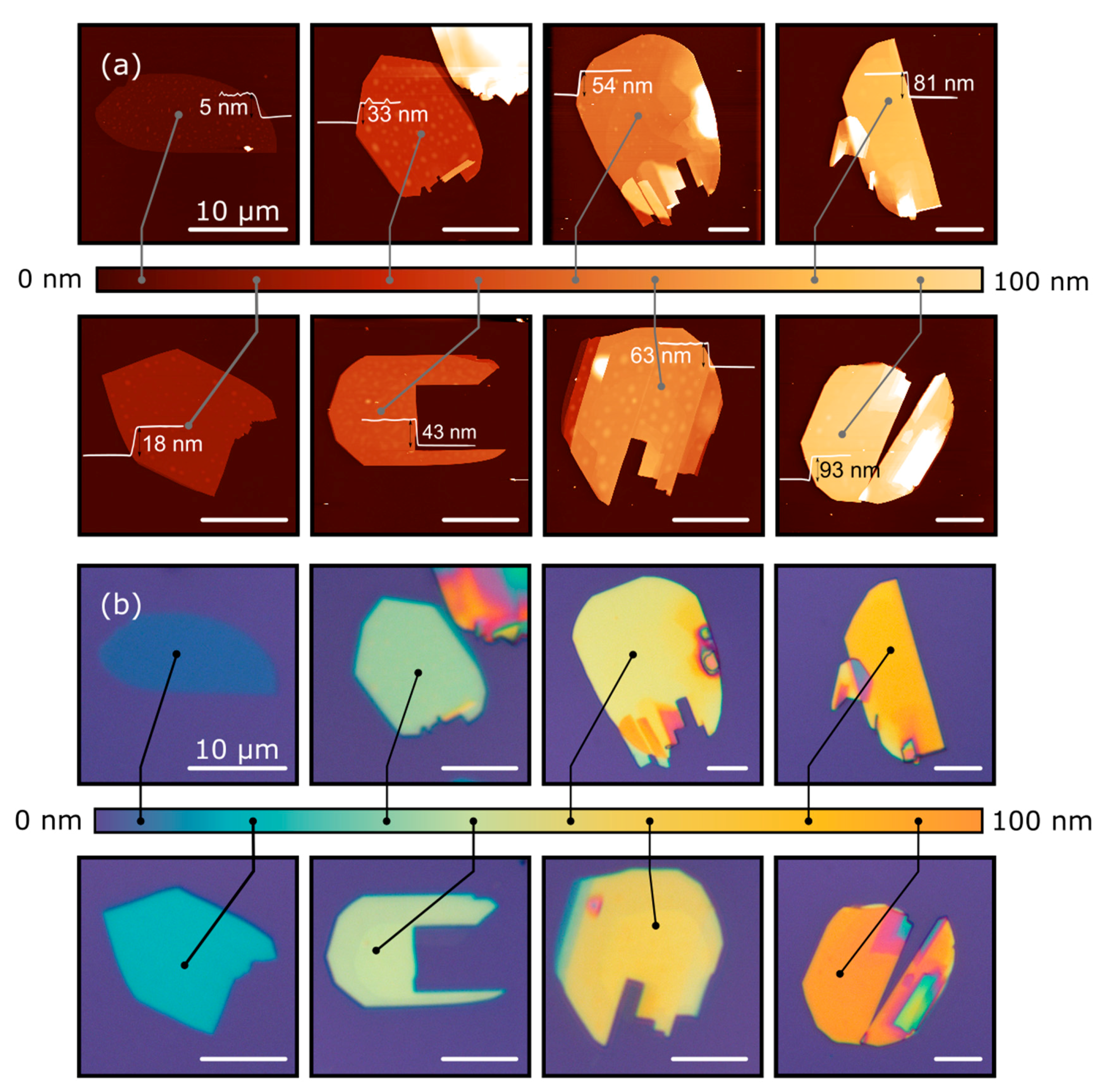
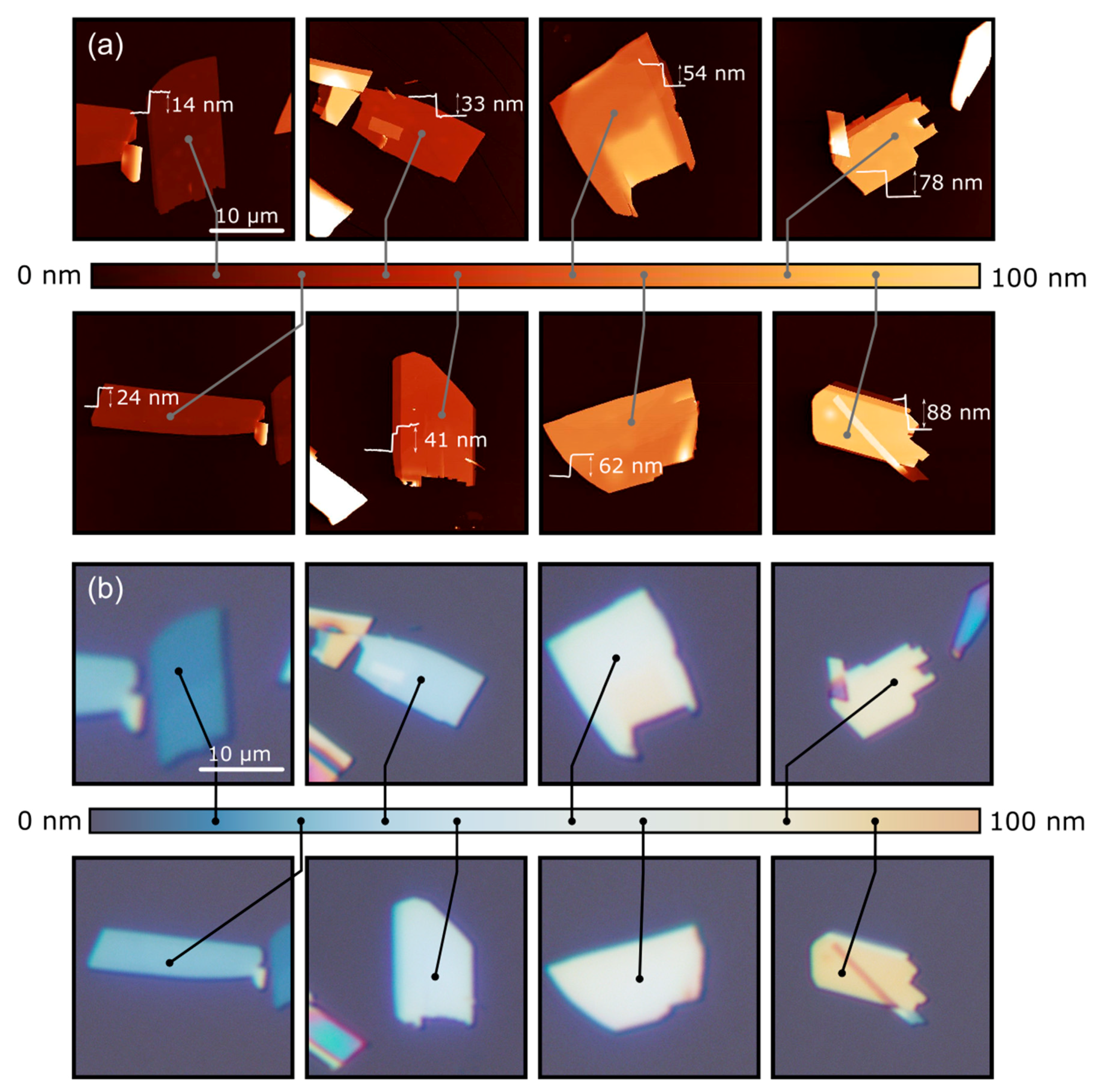
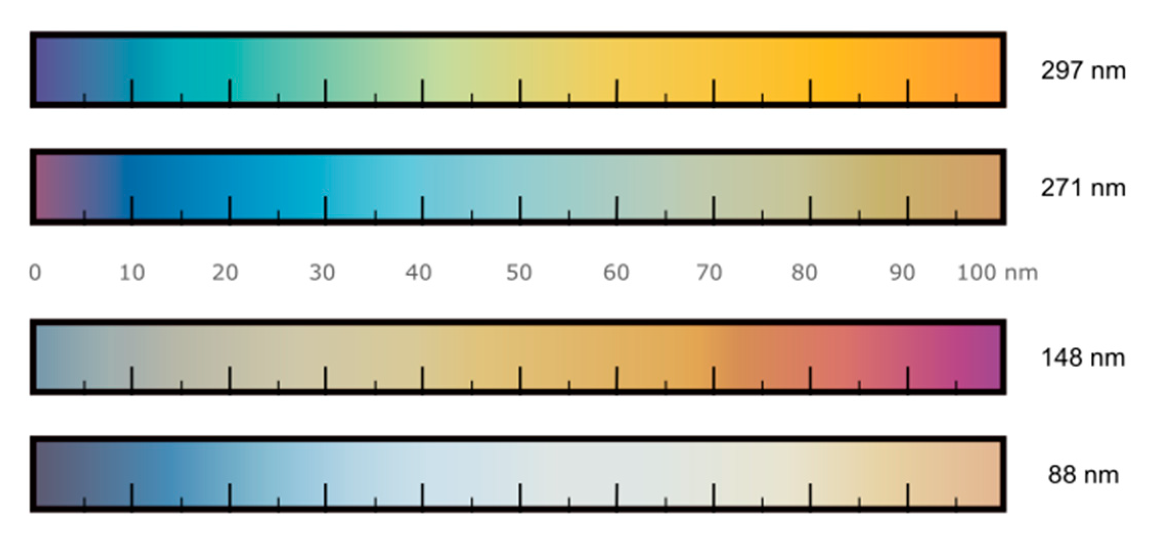
Figure 1a shows the atomic force microscopy (AFM) topography of eight MoO3 flakes with different thicknesses, and Figure 1b shows their corresponding optical microscopy images. The direct comparison between the AFM and the optical images allows us to build up a color-chart correlating the apparent color of the MoO3 flakes deposited on top of the 297 nm SiO2/Si substrate (the SiO2 thickness is experimentally measured by reflectometry with ±0.5 nm uncertainty) with their corresponding thickness with an uncertainty of ±3 nm. Similar approaches have been reported for graphene [45], transition metal dichalcogenides [46], TiS3 [47] and franckeite [48]. This method has the main limitation that it requires the use of a specific SiO2 thickness as the interference colors of the MoO3 flakes strongly depend on the underlying substrate. In this work, we provide color-charts for four different nominal SiO2 capping layer thicknesses: 297 nm, 271 nm, 148 nm and 88 nm. Figure 2 shows the correlation of optical images and AFM images for MoO3 flakes transferred onto an 88 nm SiO2/Si substrate. We address the reader to the Supporting Information for the data corresponding to the 148 nm and 271 nm thick SiO2 substrates, named as Figures S1 and S2, respectively. Figure 3 shows a comparison between the apparent color vs. the thickness color-charts obtained for the four different SiO2 thicknesses studied here. If a different SiO2 thickness is used, a new calibration measurement, like that shown in Figure 1, has to be carried out again for the desired SiO2 thickness.
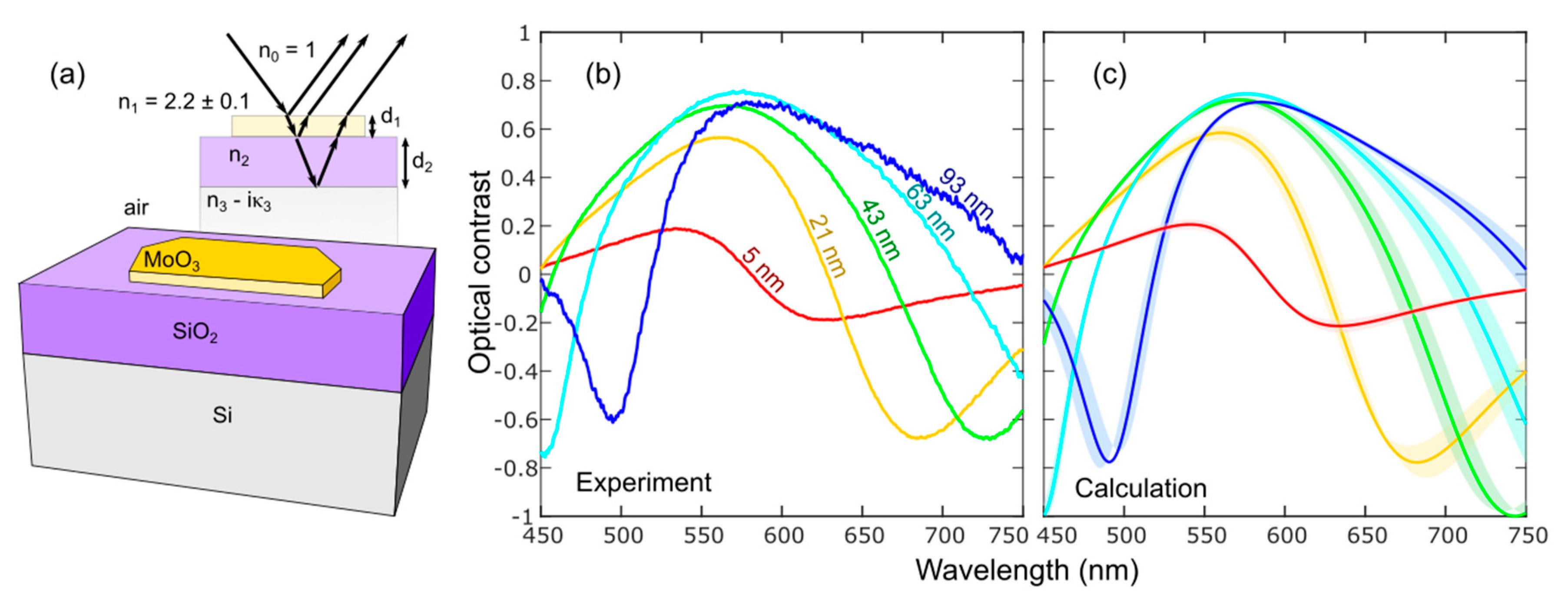
Further, we quantitatively analyze the reflection spectra of MoO3 flakes to measure their thickness more accurately, similarly to previous works in transition metal dichalcogenides, muscovite mica and black phosphorus [44,49,50,51]. Differential reflectance spectra are acquired in normal incidence with a modified metallurgical microscope (BA 310 MET-T, Motic), details in Reference [44]. A spectrum is first acquired onto the bare substrate (Is) and then onto the flake (If) and the optical contrast (C) can be calculated as:
In Figure 4a, we sketch the optical system, indicating the different optical media, used to model the optical contrast spectra. The refractive index values of the different media used for the model are shown in Figure S3a. Figure 4b shows the experimental optical contrast obtained for different values of thickness of MoO3.
The optical contrast of this kind of multilayer optical system can be calculated with high accuracy using a Fresnel law-based model [54]. The reflection coefficient in a four media Fresnel model is expressed as [55]:
where sub index 0 refers to air, 1 to MoO3, 2 to SiO2 and 3 to Si. Assuming normal incidence, Φi = 2πñidi/λ is the phase shift induced by the propagation of the light beam in the media i, being and the complex refractive index, thickness of the media and wavelength, respectively; rij = (ñi − ñj)/(ñi + ñj) is the Fresnel coefficient at the interface between the media i and j.
The reflection coefficient in a three media Fresnel model (i.e., the case of the bare substrate without the MoO3 flake) is expressed as:
where sub index 0 is air, 1 is SiO2 and 2 is Si. With these equations, one can calculate the optical contrast by firstly calculating the reflected intensity:
Then the optical contrast can be defined through the following operation that correlates the reflected intensity by the bare substrate (R3) with the reflected intensity by the MoO3 flake (R4) as:
Interestingly, we found that one can accurately reproduce the experimental optical contrast spectra by simply assuming a refractive index of MoO3 of ñ1 = 2.2 − i0. Note that, according to Reference [35], the band structure of MoO3 has a negligible thickness dependence and thus we do not expect the refractive index to depend on the flake thickness. The results of the calculated spectra with this model are depicted in Figure 4c. The real part of the refractive index of bulk MoO3 nMoO3 spans in the literature from 1.8 to 2.3 [14,56,57]. Since the literature values of the extinction coefficient in the visible range are very low, we neglect that term in our calculations, still providing a good fit to the experimental data. As verification, Figure S3b shows the complex refractive index as a function of wavelength, ñ = n + iκ, measured with ellipsometry of polycrystalline MoO3 films showing values of n = 2–2.3 in the visible part of the spectrum (from 1.5 to 3 eV) and a negligible value of κ in the same region (from 0.02 to 0.1). This ellipsometry measurement on polycrystalline MoO3 verifies that the assumed refractive index for single crystalline MoO3 flakes (ñ1 = 2.2 − i0) is reasonable.
Some of the features present in the optical contrast spectra, like the local maxima and minima, strongly depend on the thickness of the MoO3 medium. In fact, the shape of the optical contrast spectra, including the maxima and minima features, arises from the interference colors effect. It is therefore clear that these features will depend on the thickness of the MoO3 flake as the optical paths of the light beams passing through flakes with different thicknesses will be different. Therefore, one can evaluate the thickness of a MoO3 flake by calculating the optical contrast according to Equations (2)–(5) for different thicknesses of MoO3 and determining the best fit by minimum squares.
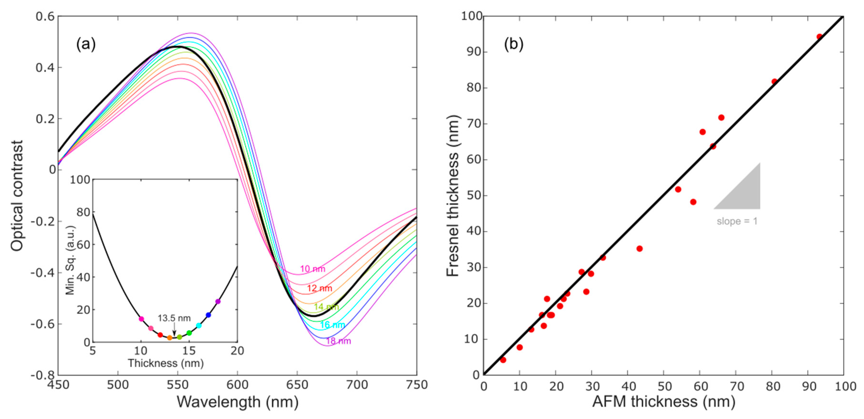
Figure 5a compares the optical contrast measured for a MoO3 flake (16.5 nm thick according to the AFM) with the optical contrast calculated assuming a thickness in the range of 0–100 nm. The best match is obtained for a thickness of 13.5 nm. The inset in Figure 5a shows the square of the difference between the measured contrast and the calculated one as a function of the thickness assumed for the calculation. The plot shows a well-defined minimum at a thickness of 13.5 nm.
In order to benchmark this thickness determination method, Figure 5b compares the thickness values measured with AFM for 23 flakes from 5 nm to 100 nm thick with the values obtained following the optical contrast fit method discussed above. In the plot, we include a straight line with a slope of 1 that indicates the perfect agreement between the thickness of MoO3 nanosheets measured by AFM and the fit to the Fresnel law-based model. The low dispersion along the slope = 1 line indicates the good agreement between the thickness evaluated by both methods. In effect, the calculated linear regression of the data points in Figure 5b has a slope of 1.02.
4. Conclusions
In summary, we provided two fast and non-destructive complementary methods to evaluate the number of layers of MoO3 nanosheets using optical microscopy. First, one can get a coarse estimation of the thickness (with ±3 nm of uncertainty) by comparing the apparent color of the flakes with a pre-calibrated color-chart. This method is very fast, but it requires the previous calibration of a color-chart that depends on the SiO2 capping layer thickness (nonetheless, we provide pre-calibrated color-charts for four commonly used SiO2 capping layer thicknesses). The second method is based on the measurement of the optical contrast spectrum of the MoO3 flake under study and the subsequent fit to a Fresnel law-based model that includes the optical constants of each medium. This method requires a modification of the optical microscope to allow for differential reflectance measurements, but it can provide lower uncertainty (±2 nm of median standard deviation for the samples on 297 nm of SiO2), and it can be easily employed for flakes transferred on SiO2/Si substrates with different SiO2 thicknesses. We believe that the development of these thickness determination methods can be very helpful for the community working on MoO3 as it can effectively speed up the research on this 2D material.
Supplementary Materials
The following are available online at https://www.mdpi.com/2079-4991/10/7/1272/s1, Figure S1: Color-chart of MoO3 on SiO2/Si with 148 nm of SiO2 capping layer, Figure S2: Color-chart of MoO3 on SiO2/Si with 271 nm of SiO2 capping layer, Figure S3: (a) Index of refraction of MoO3 films, SiO2 and Si materials. These values are obtained from bibliography [56,57,58,59] and they are in accordance with our spectroscopic ellipsometry measurements. (b) Index of refraction (n) and extinction coefficient (κ) measured by ellipsometry on a pollycrystalline α-MoO3 film transferred onto a SiO2/Si substrate with 280 nm of SiO2 thickness layer, Figure S4: Calculated optical contrast dependence on illumination wavelength and SiO2 thickness for a monolayer MoO3 on a SiO2/Si substrate.
Author Contributions
S.P. fabricated the MoO3 flake samples and performed the experimental work. A.M.-J. and R.S.G. performed the ellipsometry measurements on the polycrystalline MoO3 film. C.M. and A.C.-G. supervised and designed the experiments. S.P. and A.C.-G. drafted the firsts version of the manuscript. All authors contributed to writing the final version of the manuscript.
Funding
This project has received funding from the European Research Council (ERC) under the European Union’s Horizon 2020 research and innovation programme (grant agreement n° 755655, ERC-StG 2017 project 2D-TOPSENSE), the European Commission, under the Graphene Flagship (Core 3, grant number 881603), the Spanish Ministry of Economy, Industry and Competitiveness through the grant MAT2017-87134-C2-2-R and partially funded by the Spanish Ministerio de Ciencia e Innovación through grant RTI2018-096498-B-I00 (MCIU/AEI/FEDER, UE). SP acknowledges the fellowship PRE2018-084818.
Conflicts of Interest
The authors declare no conflicts of interest.
References
- Novoselov, K.S.; Geim, A.K.; Morozov, S.V.; Jiang, D.; Zhang, Y.; Dubonos, S.V.; Grigorieva, I.V.; Firsov, A.A. Electric field effect in atomically thin carbon films. Science 2004, 306, 666–669. [Google Scholar] [CrossRef] [Green Version]
- Burzurí, E.; Prins, F.; van der Zant, H.S.J. Characterization of Nanometer-Spaced Few-Layer Graphene Electrodes. Graphene 2012, 01, 26–29. [Google Scholar] [CrossRef] [Green Version]
- Tsai, D.S.; Liu, K.K.; Lien, D.H.; Tsai, M.L.; Kang, C.F.; Lin, C.A.; Li, L.J.; He, J.H. Few-layer MoS2 with high broadband photogain and fast optical switching for use in harsh environments. ACS Nano 2013, 7, 3905–3911. [Google Scholar] [CrossRef] [PubMed]
- Dean, C.R.; Young, A.F.; Meric, I.; Lee, C.; Wang, L.; Sorgenfrei, S.; Watanabe, K.; Taniguchi, T.; Kim, P.; Shepard, K.L.; et al. Boron nitride substrates for high-quality graphene electronics. Nat. Nanotechnol. 2010, 5, 722–726. [Google Scholar] [CrossRef]
- Akhtar, M.; Anderson, G.; Zhao, R.; Alruqi, A.; Mroczkowska, J.E.; Sumanasekera, G.; Jasinski, J.B. Recent advances in synthesis, properties, and applications of phosphorene. npj 2D Mater. Appl. 2017, 1–12. [Google Scholar] [CrossRef]
- De Castro, I.A.; Datta, R.S.; Ou, J.Z.; Castellanos-Gomez, A.; Sriram, S.; Daeneke, T.; Kalantar-zadeh, K. Molybdenum Oxides – From Fundamentals to Functionality. Adv. Mater. 2017, 29, 1–31. [Google Scholar] [CrossRef] [PubMed]
- Stanford, M.G.; Rack, P.D.; Jariwala, D. Emerging nanofabrication and quantum confinement techniques for 2D materials beyond graphene. npj 2D Mater. Appl. 2018, 2, 20. [Google Scholar] [CrossRef] [Green Version]
- Naguib, M.; Mochalin, V.N.; Barsoum, M.W.; Gogotsi, Y. 25th anniversary article: MXenes: A new family of two-dimensional materials. Adv. Mater. 2014, 26, 992–1005. [Google Scholar] [CrossRef]
- Duan, X.; Wang, C.; Pan, A.; Yu, R.; Duan, X. Two-dimensional transition metal dichalcogenides as atomically thin semiconductors: opportunities and challenges. Chem. Soc. Rev. 2015, 44, 8859–8876. [Google Scholar] [CrossRef]
- Yu, X.; Marks, T.J.; Facchetti, A. Metal oxides for optoelectronic applications. Nat. Mater. 2016, 15, 383–396. [Google Scholar] [CrossRef]
- Cai, L.; McClellan, C.J.; Koh, A.L.; Li, H.; Yalon, E.; Pop, E.; Zheng, X. Rapid flame synthesis of atomically thin MoO3 down to monolayer thickness for effective hole doping of WSe2. Nano Lett. 2017, 17, 3854–3861. [Google Scholar] [CrossRef]
- Kim, J.H.; Dash, J.K.; Kwon, J.; Hyun, C.; Kim, H.; Ji, E.; Lee, G.H. Van der Waals epitaxial growth of single crystal α-MoO3 layers on layered materials growth templates. 2D Mater. 2019, 6. [Google Scholar] [CrossRef]
- Balendhran, S.; Walia, S.; Nili, H.; Ou, J.Z.; Zhuiykov, S.; Kaner, R.B.; Sriram, S.; Bhaskaran, M.; Kalantar-Zadeh, K. Two-dimensional molybdenum trioxide and dichalcogenides. Adv. Funct. Mater. 2013, 23, 3952–3970. [Google Scholar] [CrossRef]
- Vos, M.F.J.; Macco, B.; Thissen, N.F.W.; Bol, A.A.; Kessels, W.M.M. (Erwin) Atomic layer deposition of molybdenum oxide from (N t Bu) 2 (NMe 2 ) 2 Mo and O 2 plasma. J. Vac. Sci. Technol. A Vac. Surf. Film. 2016, 34, 01A103. [Google Scholar] [CrossRef] [Green Version]
- Hussain, O.M.; Rao, K.S. Characterization of activated reactive evaporated MoO3 thin films for gas sensor applications. Mater. Chem. Phys. 2003, 80, 638–646. [Google Scholar] [CrossRef]
- Zhang, W.B.; Qu, Q.; Lai, K. High-mobility transport anisotropy in few-layer MoO3 and its origin. ACS Appl. Mater. Interfaces 2017, 9, 1702–1709. [Google Scholar] [CrossRef] [PubMed]
- You, H.; Dai, Y.; Zhang, Z.; Ma, D. Improved performances of organic light-emitting diodes with metal oxide as anode buffer. J. Appl. Phys. 2007, 101, 1–4. [Google Scholar] [CrossRef]
- Shin, W.J.; Lee, J.Y.; Kim, J.C.; Yoon, T.H.; Kim, T.S.; Song, O.K. Bulk and interface properties of molybdenum trioxide-doped hole transporting layer in organic light-emitting diodes. Org. Electron. 2008, 9, 333–338. [Google Scholar] [CrossRef]
- Tseng, Y.C.; Mane, A.U.; Elam, J.W.; Darling, S.B. Ultrathin molybdenum oxide anode buffer layer for organic photovoltaic cells formed using atomic layer deposition. Sol. Energy Mater. Sol. Cells 2012, 99, 235–239. [Google Scholar] [CrossRef]
- Zhao, Y.; Nardes, A.M.; Zhu, K. Effective hole extraction using MoO x -Al contact in perovskite CH 3 NH 3 PbI 3 solar cells. Appl. Phys. Lett. 2014, 104, 213906. [Google Scholar] [CrossRef]
- Battaglia, C.; de Nicolás, S.M.; De Wolf, S.; Yin, X.; Zheng, M.; Ballif, C.; Javey, A. Silicon heterojunction solar cell with passivated hole selective MoO x contact. Appl. Phys. Lett. 2014, 104, 113902. [Google Scholar] [CrossRef] [Green Version]
- Gurlo, A.; Bârsan, N.; Ivanovskaya, M.; Weimar, U.; Göpel, W. In2O3 and MoO3-In2O3 thin film semiconductor sensors: Interaction with NO2 and O3. Sens. Actuators B Chem. 1998, 47, 92–99. [Google Scholar] [CrossRef]
- Ferroni, M.; Guidi, V.; Martinelli, G.; Nelli, P.; Sacerdoti, M.; Sberveglieri, G. Characterization of a molybdenum oxide sputtered thin film as a gas sensor. Thin Solid Films 1997, 307, 148–151. [Google Scholar] [CrossRef]
- Quevedo-Lopez, M.A.; Reidy, R.F.; Orozco-Teran, R.A.; Mendoza-Gonzalez, O.; Ramirez-Bon, R. Enhancement of the photochromic and thermochromic properties of molybdenum oxide thin films by a cadmium sulfide underlayer. J. Mater. Sci. Mater. Electron. 2000, 11, 151–155. [Google Scholar] [CrossRef]
- Scarminio, J.; Lourenço, A.; Gorenstein, A. Electrochromism and photochromism in amorphous molybdenum oxide films. Thin Solid Films 1997, 302, 66–70. [Google Scholar] [CrossRef]
- Ivanova, T.; Gesheva, K.A.; Popkirov, G.; Ganchev, M.; Tzvetkova, E. Electrochromic properties of atmospheric CVD MoO3 and MoO 3-WO3 films and their application in electrochromic devices. Proc. Mater. Sci. Eng. B Solid State Mater. Adv. Technol. 2005, 119, 232–239. [Google Scholar] [CrossRef]
- Yao, J.N.; Hashimoto, K.; Fujishima, A. Photochromism induced in an electrolytically pretreated Mo03 thin film by visible light. Nature 1992, 355, 624–626. [Google Scholar] [CrossRef]
- He, T.; Yao, J. Photochromism of molybdenum oxide. J. Photochem. Photobiol. C Photochem. Rev. 2003, 4, 125–143. [Google Scholar] [CrossRef]
- Pham, T.T.P.; Nguyen, P.H.D.; Vo, T.T.; Luu, C.L.; Nguyen, H.H.P. Preparation of NO-doped β-MoO3 and its methanol oxidation property. Mater. Chem. Phys. 2016, 184, 5–11. [Google Scholar] [CrossRef]
- Mizushima, T.; Moriya, Y.; Phuc, N.H.H.; Ohkita, H.; Kakuta, N. Soft chemical transformation of α-MoO3 to β-MoO3 as a catalyst for vapor-phase oxidation of methanol. Catal. Commun. 2011, 13, 10–13. [Google Scholar] [CrossRef]
- Mizushima, T.; Fukushima, K.; Ohkita, H.; Kakuta, N. Synthesis of β-MoO3 through evaporation of HNO3-added molybdic acid solution and its catalytic performance in partial oxidation of methanol. Appl. Catal. A Gen. 2007, 326, 106–112. [Google Scholar] [CrossRef]
- Phuong, P.T.T.; Duy, N.P.H. Facile synthesis of a green metastable MoO 3 for the selective oxidation of methanol to formaldehyde. React. Kinet. Mech. Catal. 2016, 117, 161–171. [Google Scholar] [CrossRef]
- Machiels, C.J.; Cheng, W.H.; Chowdhry, U.; Farneth, W.E.; Hong, F.; Mc Carron, E.M.; Sleight, A.W. The effect of the structure of molybdenum oxides on the selective oxidation of methanol. Appl. Catal. 1986, 25, 249–256. [Google Scholar] [CrossRef]
- Zhang, J.; Pan, Y.; Chen, Y.; Lu, H. Plasmonic molybdenum trioxide quantum dots with noble metal-comparable surface enhanced Raman scattering. J. Mater. Chem. C 2018, 6, 2216–2220. [Google Scholar] [CrossRef]
- Molina-Mendoza, A.J.; Lado, J.L.; Island, J.O.; Niño, M.A.; Aballe, L.; Foerster, M.; Bruno, F.Y.; López-Moreno, A.; Vaquero-Garzon, L.; van der Zant, H.S.J.; et al. Centimeter-Scale Synthesis of Ultrathin Layered MoO3 by van der Waals Epitaxy. Chem. Mater. 2016, 28, 4042–4051. [Google Scholar] [CrossRef] [Green Version]
- Kalantar-Zadeh, K.; Tang, J.; Wang, M.; Wang, K.L.; Shailos, A.; Galatsis, K.; Kojima, R.; Strong, V.; Lech, A.; Wlodarski, W.; et al. Synthesis of nanometre-thick MoO3 sheets. Nanoscale 2010, 2, 429–433. [Google Scholar] [CrossRef]
- Zheng, B.; Wang, Z.; Chen, Y.; Zhang, W.; Li, X. Centimeter-sized 2D α -MoO 3 single crystal: growth, Raman anisotropy, and optoelectronic properties. 2D Mater. 2018, 5, 045011. [Google Scholar] [CrossRef]
- Reed, B.W.; Williams, D.R.; Moser, B.P.; Koski, K.J. Chemically Tuning Quantized Acoustic Phonons in 2D Layered MoO3 Nanoribbons. Nano Lett. 2019, 19, 4406–4412. [Google Scholar] [CrossRef]
- Zheng, Q.; Ren, P.; Peng, Y.; Zhou, W.; Yin, Y.; Wu, H.; Gong, W.; Wang, W.; Tang, D.; Zou, B. In-Plane Anisotropic Raman Response and Electrical Conductivity with Robust Electron-Photon and Electron-Phonon Interactions of Air Stable MoO 2 Nanosheets. J. Phys. Chem. Lett. 2019, 10, 2182–2190. [Google Scholar] [CrossRef]
- Yuan, H.; Liu, X.; Afshinmanesh, F.; Li, W.; Xu, G.; Sun, J.; Lian, B.; Curto, A.G.; Ye, G.; Hikita, Y.; et al. Polarization-sensitive broadband photodetector using a black phosphorus vertical p-n junction. Nat. Nanotechnol. 2015, 10, 707–713. [Google Scholar] [CrossRef] [Green Version]
- Wang, X.; Li, Y.; Huang, L.; Jiang, X.W.; Jiang, L.; Dong, H.; Wei, Z.; Li, J.; Hu, W. Short-Wave Near-Infrared Linear Dichroism of Two-Dimensional Germanium Selenide. J. Am. Chem. Soc. 2017, 139, 14976–14982. [Google Scholar] [CrossRef] [PubMed]
- Ma, W.; Alonso-González, P.; Li, S.; Nikitin, A.Y.; Yuan, J.; Martín-Sánchez, J.; Taboada-Gutiérrez, J.; Amenabar, I.; Li, P.; Vélez, S.; et al. In-plane anisotropic and ultra-low-loss polaritons in a natural van der Waals crystal. Nature 2018, 562, 557–562. [Google Scholar] [CrossRef] [PubMed] [Green Version]
- Horcas, I.; Fernández, R.; Gómez-Rodríguez, J.M.; Colchero, J.; Gómez-Herrero, J.; Baro, A.M. WSXM: A software for scanning probe microscopy and a tool for nanotechnology. Rev. Sci. Instrum. 2007, 78, 013705. [Google Scholar] [CrossRef] [PubMed]
- Frisenda, R.; Niu, Y.; Gant, P.; Molina-Mendoza, A.J.; Schmidt, R.; Bratschitsch, R.; Liu, J.; Fu, L.; Dumcenco, D.; Kis, A.; et al. Micro-reflectance and transmittance spectroscopy: a versatile and powerful tool to characterize 2D materials. J. Phys. D. Appl. Phys. 2017, 50, 074002. [Google Scholar] [CrossRef]
- Li, X.; Cai, W.; An, J.; Kim, S.; Nah, J.; Yang, D.; Piner, R.; Velamakanni, A.; Jung, I.; Tutuc, E.; et al. Large-area synthesis of high-quality and uniform graphene films on copper foils. Science 2009, 324, 1312–1314. [Google Scholar] [CrossRef] [Green Version]
- Li, H.; Wu, J.; Huang, X.; Lu, G.; Yang, J.; Lu, X.; Xiong, Q.; Zhang, H. Rapid and reliable thickness identification of two-dimensional nanosheets using optical microscopy. ACS Nano 2013, 7, 10344–10353. [Google Scholar] [CrossRef] [PubMed] [Green Version]
- Papadopoulos, N.; Frisenda, R.; Biele, R.; Flores, E.; Ares, J.R.; Sánchez, C.; Van Der Zant, H.S.J.; Ferrer, I.J.; D’Agosta, R.; Castellanos-Gomez, A. Large birefringence and linear dichroism in TiS3 nanosheets. Nanoscale 2018, 10. [Google Scholar] [CrossRef] [Green Version]
- Gant, P.; Ghasemi, F.; Maeso, D.; Munuera, C.; López-Elvira, E.; Frisenda, R.; De Lara, D.P.; Rubio-Bollinger, G.; Garcia-Hernandez, M.; Castellanos-Gomez, A. Optical contrast and refractive index of natural van der Waals heterostructure nanosheets of franckeite. Beilstein J. Nanotechnol. 2017, 8, 2357–2362. [Google Scholar] [CrossRef]
- Rubio-Bollinger, G.; Guerrero, R.; de Lara, D.; Quereda, J.; Vaquero-Garzon, L.; Agraït, N.; Bratschitsch, R.; Castellanos-Gomez, A. Enhanced Visibility of MoS2, MoSe2, WSe2 and Black-Phosphorus: Making Optical Identification of 2D Semiconductors Easier. Electronics 2015, 4, 847–856. [Google Scholar] [CrossRef] [Green Version]
- Niu, Y.; Gonzalez-Abad, S.; Frisenda, R.; Marauhn, P.; Drüppel, M.; Gant, P.; Schmidt, R.; Taghavi, N.; Barcons, D.; Molina-Mendoza, A.; et al. Thickness-Dependent Differential Reflectance Spectra of Monolayer and Few-Layer MoS2, MoSe2, WS2 and WSe2. Nanomaterials 2018, 8, 725. [Google Scholar] [CrossRef] [Green Version]
- Castellanos-Gomez, A.; Wojtaszek, M.; Tombros, N.; Agrait, N.; van Wees, B.J.; Rubio-Bollinger, G. Atomically thin mica flakes and their application as ultrathin insulating substrates for graphene. Small 2011, 7, 2491–2497. [Google Scholar] [CrossRef] [PubMed] [Green Version]
- Ares, P.; Zamora, F.; Gomez-Herrero, J. Optical Identification of Few-Layer Antimonene Crystals. ACS Photonics 2017, 4, 600–605. [Google Scholar] [CrossRef] [Green Version]
- Backes, C.; Abdelkader, A.M.; Alonso, C.; Andrieux-Ledier, A.; Arenal, R.; Azpeitia, J.; Balakrishnan, N.; Banszerus, L.; Barjon, J.; Bartali, R. Production and processing of graphene and related materials. 2D Mater. 2020, 7, 22001. [Google Scholar] [CrossRef]
- Hecht, E. Optics, 4th ed.; Addison Wesley: Boston, MA, USA, 2002; ISBN 0-321-18878-0. [Google Scholar]
- Anders, H. Thin Films in Optics; Focal Press: London, UK, 1967; ISBN 024044793X. [Google Scholar]
- Szekeres, A.; Ivanova, T.; Gesheva, K. Spectroscopic ellipsometry study of CVD molybdenum oxide films: effect of temperature. J. Solid State Electrochem. 2002, 7, 17–20. [Google Scholar] [CrossRef]
- Deb, S.K.; A, P.R.S.L. Physical properties of a transition metal oxide: optical and photoelectric properties of single crystal and thin film molybdenum trioxide. Proc. R. Soc. Lond. Ser. A Math. Phys. Sci. 1968, 304, 211–231. [Google Scholar] [CrossRef]
- Schinke, C.; Christian Peest, P.; Schmidt, J.; Brendel, R.; Bothe, K.; Vogt, M.R.; Kröger, I.; Winter, S.; Schirmacher, A.; Lim, S.; et al. Uncertainty analysis for the coefficient of band-to-band absorption of crystalline silicon. AIP Adv. 2015, 5, 067168. [Google Scholar] [CrossRef] [Green Version]
- Malitson, I.H. Interspecimen Comparison of the Refractive Index of Fused Silica*,†. J. Opt. Soc. Am. 1965, 55. [Google Scholar] [CrossRef]
Figure 1.
Thickness dependent apparent color of MoO3 flakes. (a) AFM measurements of the exfoliated flakes with different thickness placed on a 297 nm SiO2/Si substrate. (b) Optical images of the flakes and a colorbar with the apparent color of flakes with thickness from 5 nm up to 93 nm (from 7 to ~130 layers). Scale bars: 10 µm.

Figure 2.
Thickness dependent apparent color of MoO3 flakes. (a) AFM measurements of the exfoliated flakes with different thickness placed on an 88 nm SiO2/Si substrate. (b) Optical images of the flakes and a colorbar with the apparent color of flakes with thickness up to 88 nm. Scale bars: 10 µm.
Figure 2.
Thickness dependent apparent color of MoO3 flakes. (a) AFM measurements of the exfoliated flakes with different thickness placed on an 88 nm SiO2/Si substrate. (b) Optical images of the flakes and a colorbar with the apparent color of flakes with thickness up to 88 nm. Scale bars: 10 µm.

Figure 3.
Thickness dependent apparent color of MoO3 flakes on SiO2/Si substrates with different oxide capping layer thickness.
Figure 3.
Thickness dependent apparent color of MoO3 flakes on SiO2/Si substrates with different oxide capping layer thickness.

Figure 4.
(a) Optical model used to calculate the MoO3 optical contrast. (b) Optical contrast spectra measured on MoO3 flakes, on a 297 nm SiO2/Si substrate, of different thickness. (c) Calculated optical contrast (solid lines) using the Fresnel law-based model [52]. The shaded area accounts for an uncertainty of ±1 nm in the thickness of the flake [53].

Figure 5.
(a) Experimental optical contrast (black) and comparison with the calculated ones (color lines) of MoO3 flakes, with thicknesses from 10 to 18 nm, placed onto a substrate of 297 nm of SiO2. Inset of figure: minimum square value for different values of thickness of the flakes. (b) Comparison of thickness measured with AFM and the Fresnel model. Experimental data represented as red dots and line in black has a slope of 1.

© 2020 by the authors. Licensee MDPI, Basel, Switzerland. This article is an open access article distributed under the terms and conditions of the Creative Commons Attribution (CC BY) license (http://creativecommons.org/licenses/by/4.0/).
Share and Cite
MDPI and ACS Style
Puebla, S.; Mariscal-Jiménez, A.; Galán, R.S.; Munuera, C.; Castellanos-Gomez, A. Optical-Based Thickness Measurement of MoO3 Nanosheets. Nanomaterials 2020, 10, 1272. https://doi.org/10.3390/nano10071272
AMA Style
Puebla S, Mariscal-Jiménez A, Galán RS, Munuera C, Castellanos-Gomez A. Optical-Based Thickness Measurement of MoO3 Nanosheets. Nanomaterials. 2020; 10(7):1272. https://doi.org/10.3390/nano10071272
Chicago/Turabian StylePuebla, Sergio, Antonio Mariscal-Jiménez, Rosalía Serna Galán, Carmen Munuera, and Andres Castellanos-Gomez. 2020. "Optical-Based Thickness Measurement of MoO3 Nanosheets" Nanomaterials 10, no. 7: 1272. https://doi.org/10.3390/nano10071272
Note that from the first issue of 2016, this journal uses article numbers instead of page numbers. See further details here.