Article

Researching the Aluminum Nitride Etching Process for Application in MEMS Resonators

1
Institute of Semiconductors, Chinese Academy of Sciences, Beijing 100083, China
2
State Key Laboratory of Transducer Technology, Chinese Academy of Sciences, Beijing 100083, China
*
Author to whom correspondence should be addressed.
Micromachines 2015, 6(2), 281-290; https://doi.org/10.3390/mi6020281
Submission received: 12 October 2014 / Accepted: 6 February 2015 / Published: 16 February 2015

Abstract

:
We investigated the aluminum nitride etching process for MEMS resonators. The process is based on Cl2/BCl3/Ar gas chemistry in inductively coupled plasma system. The hard mask of SiO2 is used. The etching rate, selectivity, sidewall angle, bottom surface roughness and microtrench are studied as a function of the gas flow rate, bias power and chamber pressure. The relations among those parameters are reported and theoretical analyses are given. By optimizing the etching parameters, the bottom surface roughness of 1.98 nm and the sidewall angle of 83° were achieved. This etching process can meet the manufacturing requirements of aluminum nitride MEMS resonator.

1. Introduction

Aluminum nitride (AlN) is an III-V group compound semiconductor material with the wide bandgap of 6.2 eV. The piezoelectric coefficient d33 is about 5.5 pm/V and d31 is about −2.6 pm/V [1]. The excellent electromechanical properties make it suitable for MEMS resonators. The film bulk acoustic wave resonators (FBAR) are widely studied and used. The resonant frequency of 1.8 GHz is achieved in FBAR [2]. Another type of resonator, the contour mode resonator (CMR), is becoming an important area of research, achieving more and more attention. The resonant frequency of CMR can be achieved as high as 10 GHz [3]. In addition, the Lamb wave resonators play an important role in MEMS resonators. This has some special advantages, such as the low motional resistance, high frequency and the multiple frequency capability. More research has been done by Chih-Ming Lin et al. [4,5,6]. With the development of wireless communication technology, the resonators should have higher resonant frequency and a higher quality factor value.
Piezoelectric AlN MEMS resonators have a “sandwich” structure: the bottom electrode layer, AlN layer and the top electrode layer. The substrate of these types of resonators is typically Si. In the manufacturing processes, the AlN etching is a key process. The etching result will strongly affect the performance parameters, such as resonant frequency and the quality factor. Recently, the inductively coupled plasma (ICP) etching process is widely used in the AlN etching process. However, there are still some problems in the process, such as poor sidewall angle, microtrenching effect and bottom roughness. Vladimir Bliznetsov et al. have done a lot of research in AlN etching. Their study shows the sidewall angle of 71.7°, the less obvious effects of microtrenching and the small bottom surface roughness of about 5–10 nm [7].
This paper focuses on the AlN etching process. The ICP etching technology was used. In this experiment, some major etching process parameters were studied. The etching results were characterized by the etching rate, selectivity, sidewall angle, bottom surface roughness and microtrenching.

2. Experimental Section

The etching sample in this experiment is polycrystalline AlN film with the thickness of 450 nm and the crystal orientation of (002). The full width of half maximum (FWHM) measured by X-ray diffraction is 1.7° and the roughness root-mean-square (RMS) is 3.2 nm measured by atomic force microscope (AFM). The grain size value is approximately 50 nm measured by scanning electron microscope (SEM). The hard mask of SiO2 with the thickness of 1 μm was used. In this paper, the selectivity is the etching rate ratio of AlN to SiO2. Chlorine-based gases were usually used in the etching process of AlN [8,9,10,11,12]. The etching products are a series of Al-Cl volatile compounds, such as AlCl3, Al2Cl6 and other Al-Cl compounds. In this experiment, the Sentech etcher was used and the etching gases are Cl2/BCl3/Ar. In the etching gases, BCl3 was added to reduce the surface roughness. The initial process parameters are Cl2/BCl3/Ar = 25/15/5 sccm, ICP source power of 700 W, bias power of 80 W and chamber pressure of 0.5 Pa. The single variability method was used in the experiment. That means that only one parameter is changed and the other parameters are fixed in each recipe. The results were measured by SEM and AFM.

3. Results and Discussion

3.1. Etching Rate and Selectivity

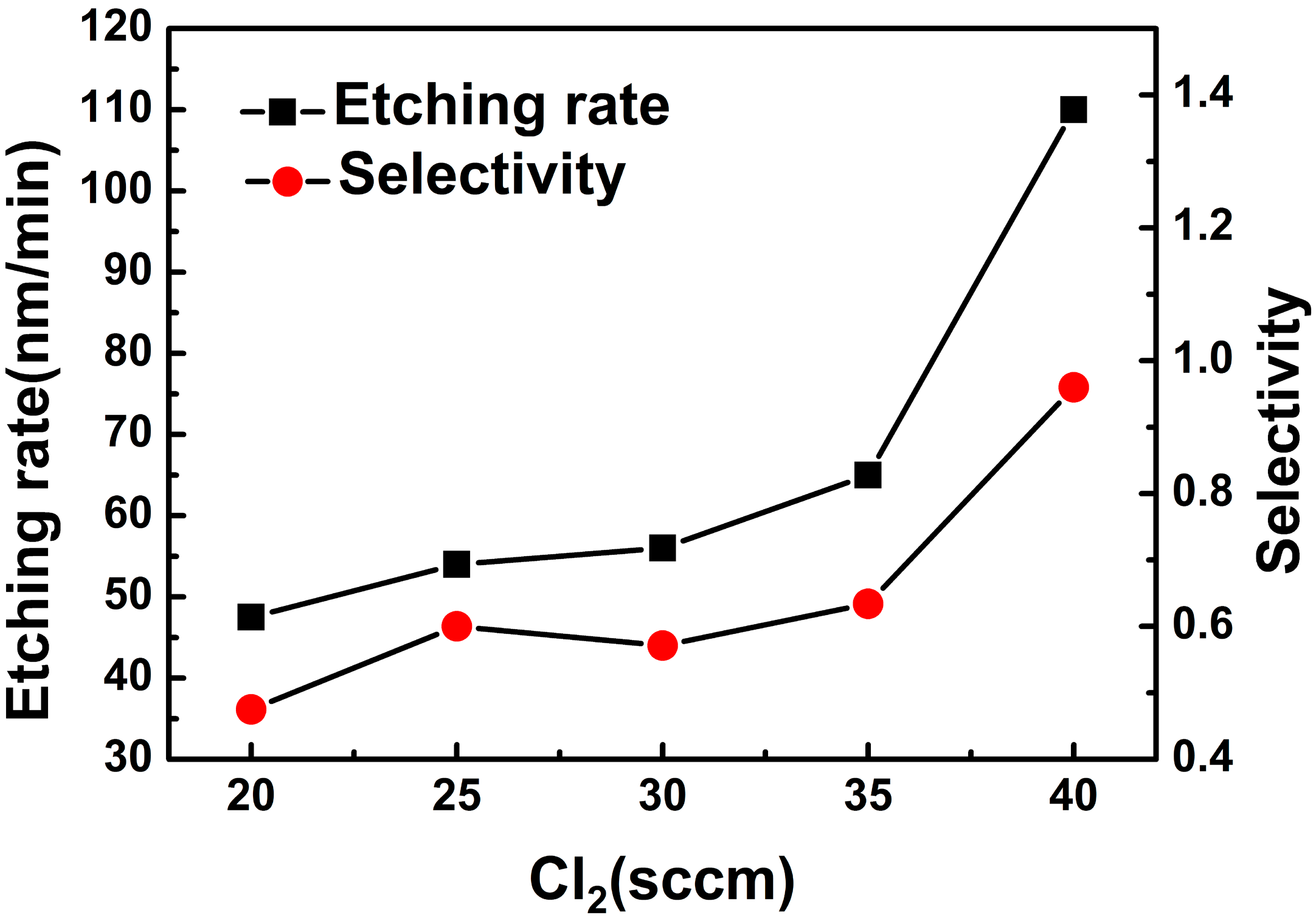
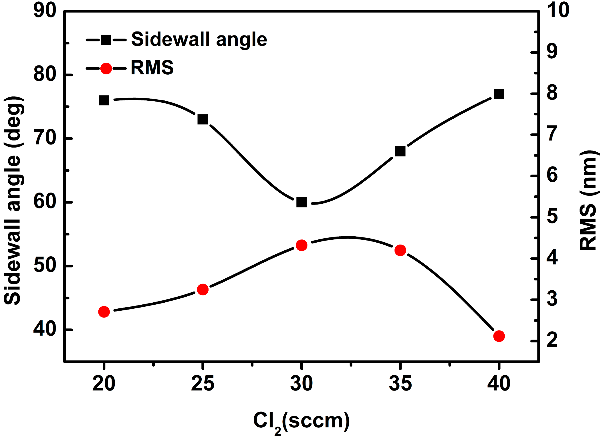
3.1.1. Cl2 Flow Rate

The etching rate and selectivity as a function of Cl2 flow rate are shown in Figure 1. The etching rate increases with the Cl2 flow rate. The value of etching rate is 47 nm/min when Cl2 flow rate is 20 sccm, whereas it increases to 110 nm/min with Cl2 flow rate 40 sccm. When other process parameters are fixed, the concentration of Cl atom and ion will increase with the increase of Cl2 flow rate. As a result, the chemical reactive etch will be enhanced, which will increase the etching rate.
Figure 1. Aluminum nitride (AlN) etching rate and selectivity versus the flow rate of Cl2.
Micromachines 06 00281 g001
The selectivity increases with the Cl2 flow rate too. It has the same trend with the etching rate versus to Cl2 flow rate. The selectivity increases from 0.5 to 1 when Cl2 flow rate increases from 20 to 40 sccm. In the etching process, the etching mechanism can be divided into two species, namely the chemical reactive etching and the physical bombardment etching. When the Cl2 flow rate is increased, the main mechanism of the etching process starts to deviate from the physical bombardment etching to chemical reactive etching. As a result, the etching rate of AlN film becomes faster. Whereas the etching rate of SiO2 is mainly decided by the physical bombardment etching, the etching rate of SiO2 mask is approximately independent of Cl2 flow rate. Thus, the selectivity increases with the increase of Cl2 flow rate.

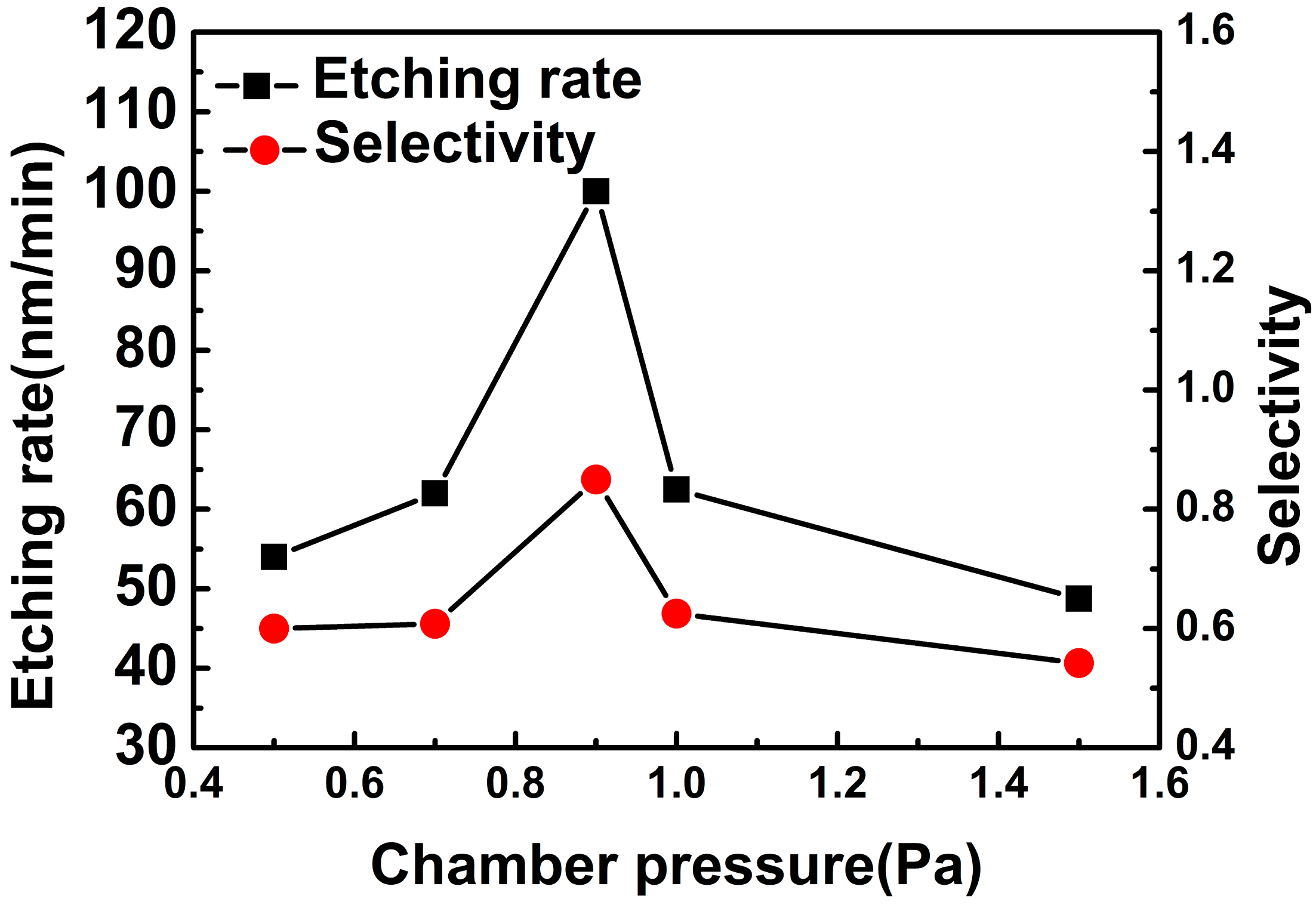
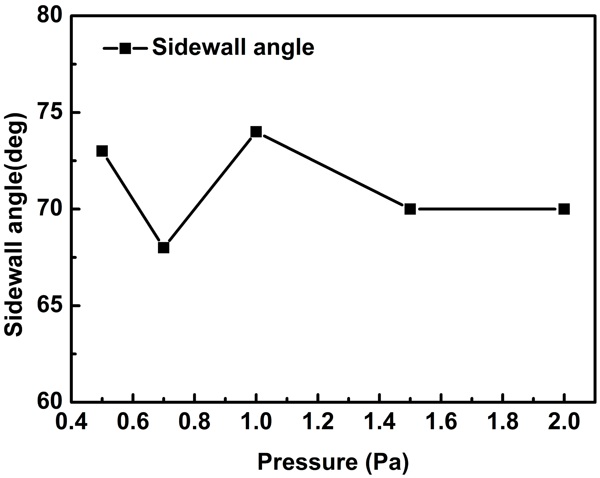
3.1.2. Chamber Pressure
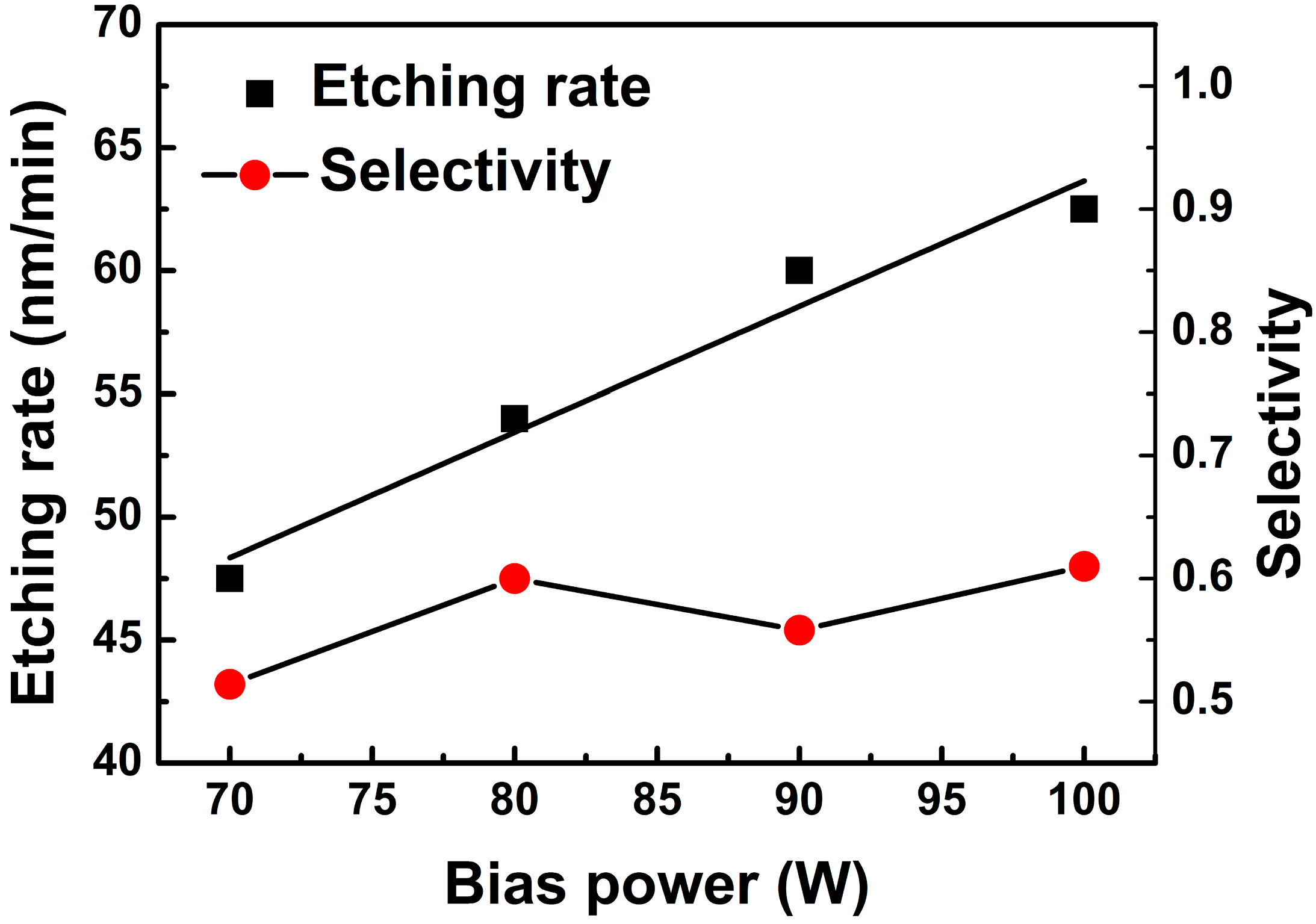
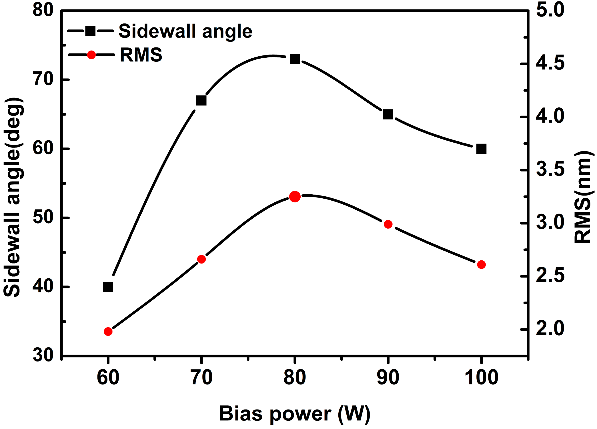
Figure 2 presents the etching rate and selectivity as a function of the chamber pressure. We note that the etching rates are shifted positively when the pressure is lower than 0.9 Pa, whereas negatively when it higher than 0.9 Pa. The chamber pressure is determined by the rate of inlet gas flow and outlet gas flow. A higher chamber pressure leads to a higher gas concentration. Thus, the etching rate increases with the increasing concentration of Cl atom and ion. However, the etching rate will shift downward with the pressure increased further. There are three reasons for this phenomenon. (1) More collisions take place between the particles when the concentration is higher, which shortens the mean free path. The kinetic energy will decrease when the etching particles move to the surface of AlN film. This reason leads to a decreased etching rate. (2) More collisions lead to more recombination between the etchant ions and atoms. This recombination will generate more stable molecules. Hence, the concentration of the active etchant will decrease. (3) Due to the fixed rate of inlet gas flow, the outlet gas flow rate will decrease to meet the increase of chamber pressure. However, the etching products cannot be exhausted immediately. Some products will attach to the surface of AlN. The etching process will be suppressed to a certain extent. This also leads to the etching rate decreased.
Figure 2. AlN etching rate and selectivity versus the chamber pressure.
Micromachines 06 00281 g002

3.1.3. Bias Power

The etching rate shows linearly increase with the bias power, as can be seen in Figure 3. The etching rate increased from 47 to 64 nm/min as the bias power was increased from 70 to 100 W. The kinetic energy of the bombardment particles is mainly dominated by the bias power. In the plasma system, the ions are accelerated by the electric field which is generated by the bias power. When the bias power is increased, the kinetic energy of the ions will be increased. The physical bombardment etching will be enhanced. As a consequence, the etching rate will linearly increase with the bias power.
Figure 3. AlN etching rate and selectivity versus the bias power.
Micromachines 06 00281 g003

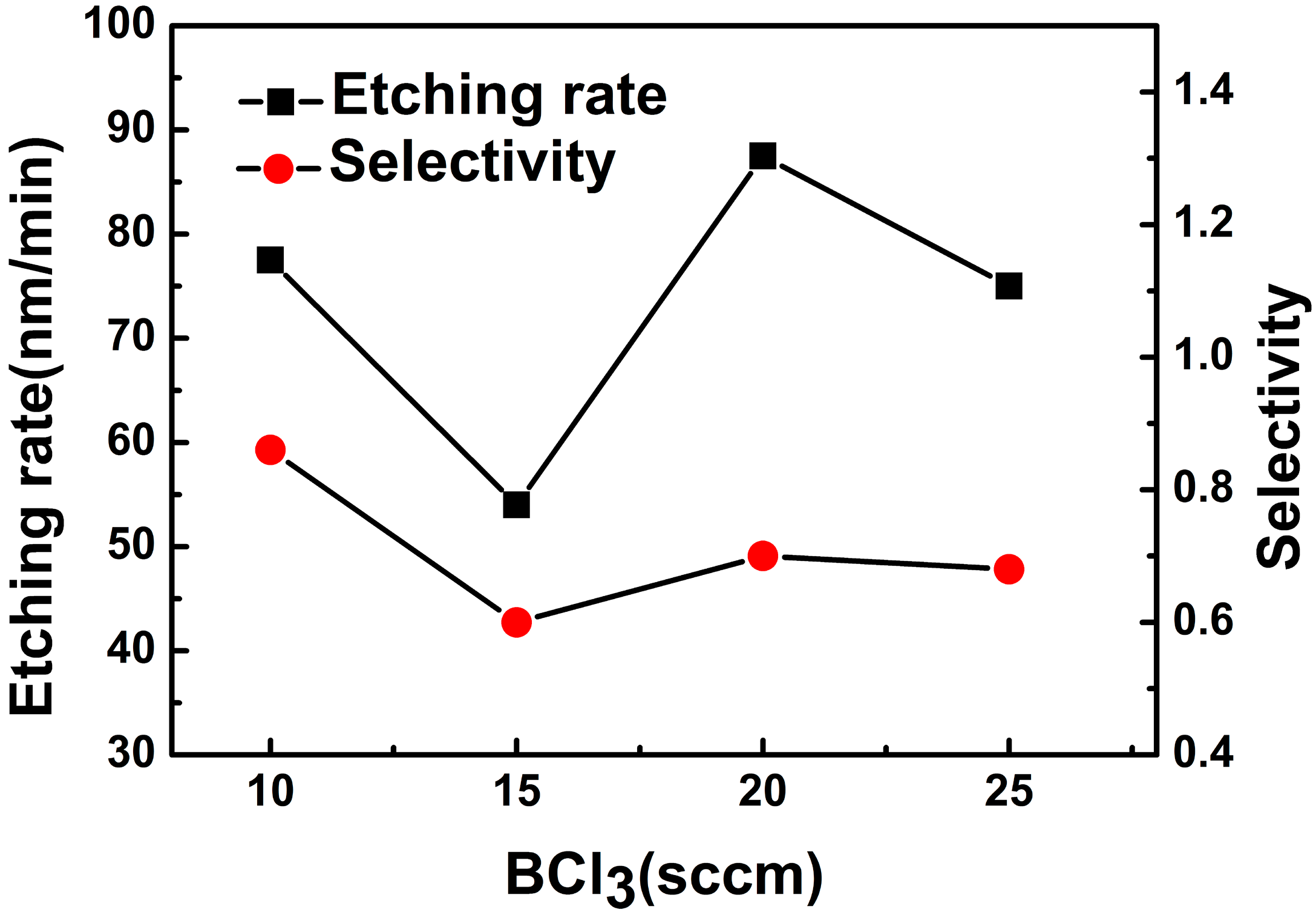
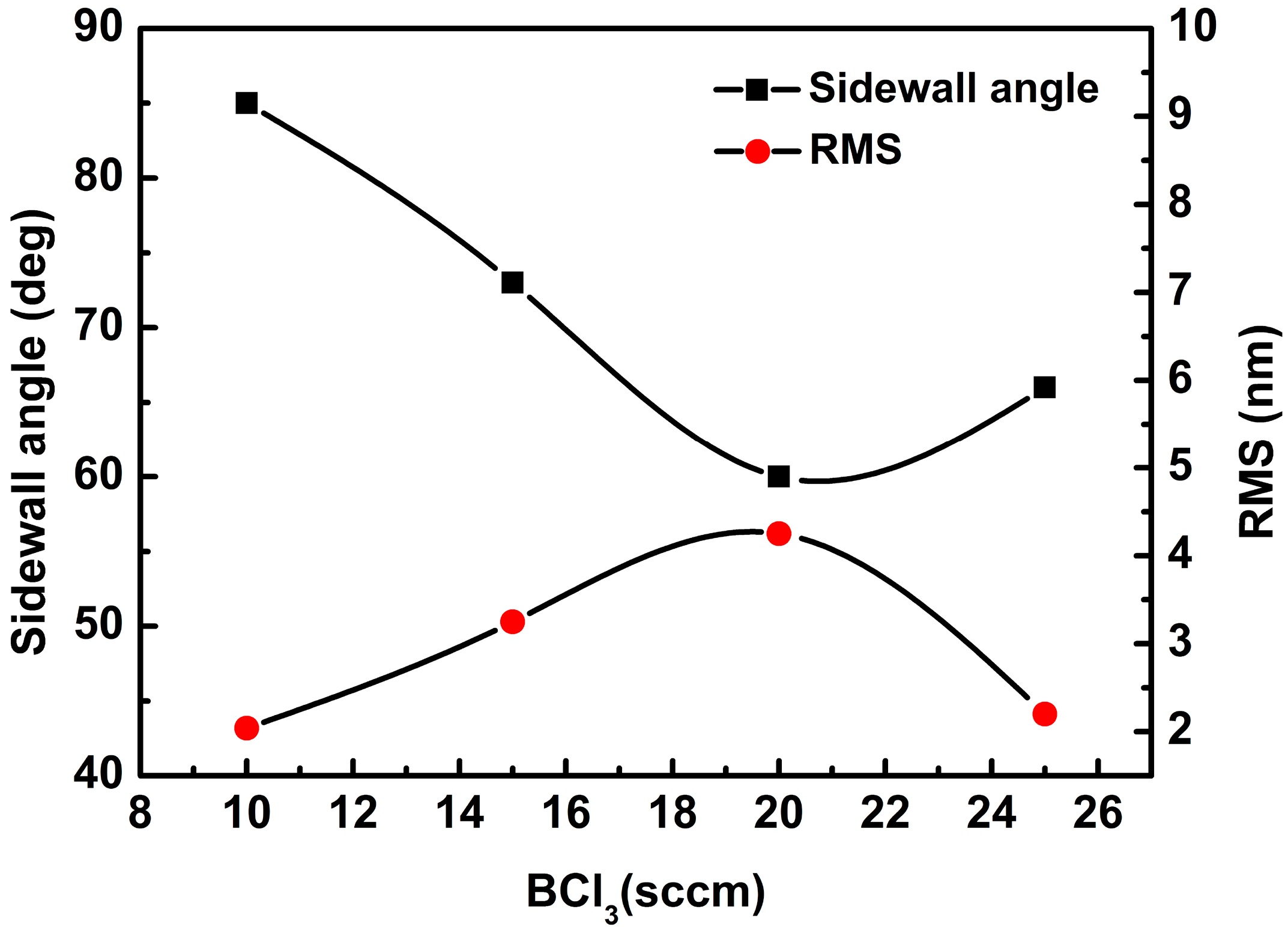
3.1.4. BCl3 Flow Rate

The etching rate and selectivity display a mixed effect with an increase of the flow rate of BCl3 as shown in Figure 4. However, the selectivity tends to a stable value with the further increase.
There is a positive correlation between the etching rate and the selectivity from the above Figure 1, Figure 2 and Figure 4. The reasons are analyzed as followed. In the etching process, the hard mask of SiO2 was etched mainly by physical bombardment etching. While AlN film was etched by both physical and chemical etching. When the chemical etching becomes the dominating mechanism, the etching rate of AlN is determined by the chemical etching. However, the etching rate of SiO2 is not obviously affected by the chemical etching. Thus, the selectivity has a positive correlation with etching rate.
However, the etching rate and selectivity do not exhibit a correlation if we only change the bias power. The main reason for this is that the physical etching mechanism will have an effect on both SiO2 and AlN etching rate. Both etching rates will be changed. Hence, there is no clear correlation between the etching rate and selectivity.
Figure 4. AlN etching rate and selectivity versus the flow rate of BCl3.
Micromachines 06 00281 g004

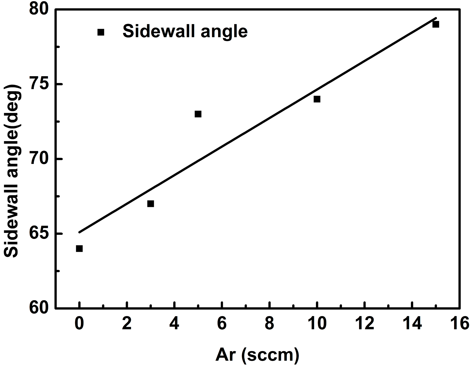
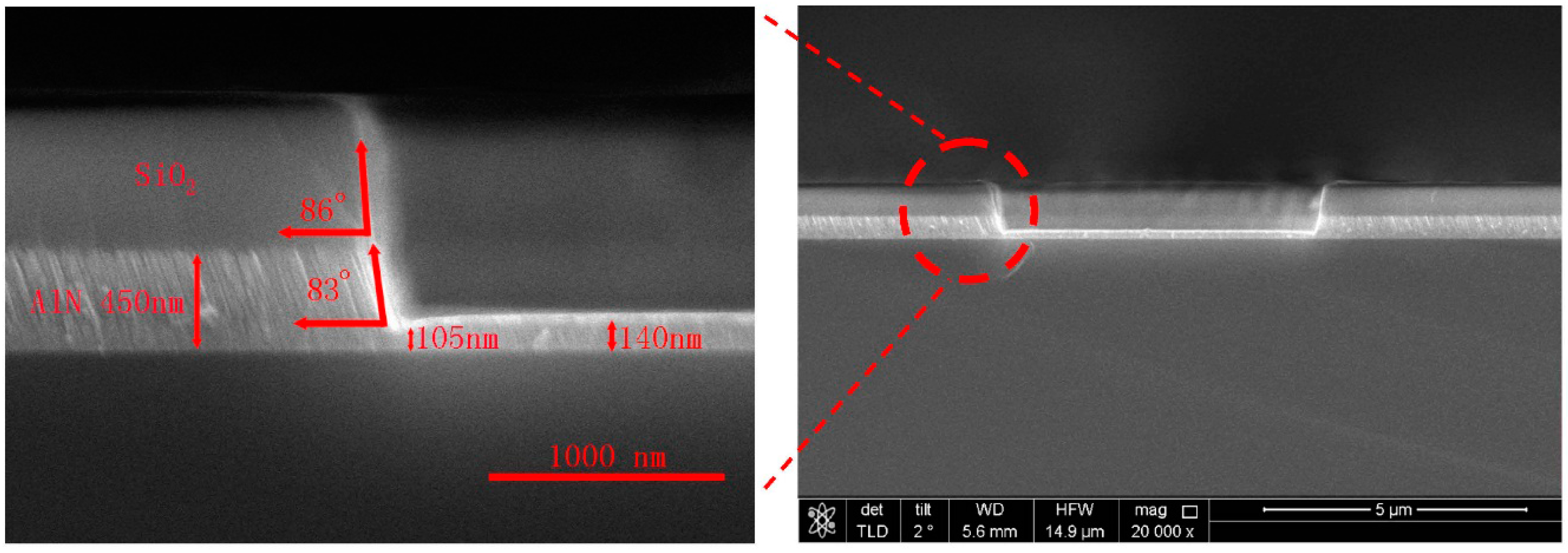
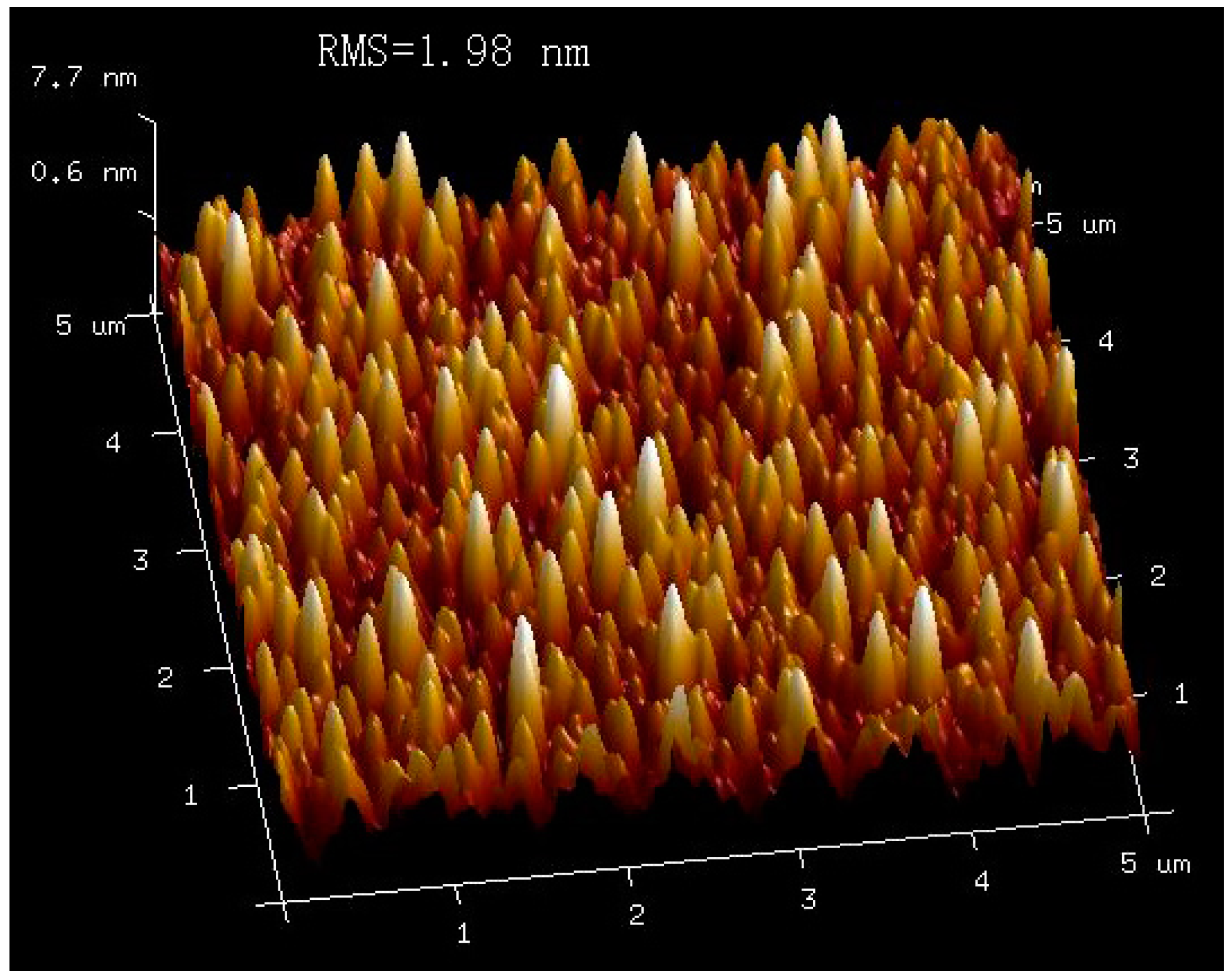
3.2. Sidewall Angle and Roughness

Figure 5 and Figure 6 present the relation between the sidewall angle and the flow rate of Cl2 as well as BCl3. It decreases with the increasing flow rate, and shifts upward with the further increase. However, the surface roughness shows the opposite trend. With the increase of Cl2 or BCl3, the RMS values first increase and then decrease.
With the increase of Cl2 or BCl3 flow rate, the chemical etching becomes the main etching mechanism. The etching rates in grains and at the grain boundaries are different. Hence, the difference between the two etching rates is enlarged with increasing concentration of Cl, which will lead to the increased surface roughness. However, the RMS trend turns to be decreased when the flow rate of Cl2 above 30 sccm (or the BCl3 flow rate above 20 sccm). Large gas flow rates lead to more particle collisions in the chamber. As a result, the energy of Cl will be reduced. Therefore, the difference of the etching rates between the grain boundaries and the inside grains will be reduced. The RMS presents a downward trend.
The relation between the sidewall angle and the bias power is shown in Figure 7. When the bias power is increased to 80 W, the sidewall angle rapidly increases to the value greater than 70°. However, when the bias power continued to increase, the sidewall angle will decrease slowly. The physical etching mechanism plays an important role in the change of the trend. In the chamber, some particles move at the direction perpendicular to the sample surface, while the others moving at an oblique direction. When the bias power lower than 80 W, with increasing bias power, the vertical etching becomes the dominating mechanism. Therefore, the sidewall angle increases rapidly. When the bias power is up to 80 W, with the further increase, the effect of oblique etching becomes obvious. Hence, the sidewall angle gradually decreases.
Figure 5. Sidewall angle and root-mean-square (RMS) versus the flow rate of Cl2.
Micromachines 06 00281 g005
Figure 6. Sidewall angle and RMS versus the flow rate of BCl3.
Micromachines 06 00281 g006
Figure 7. Sidewall angle and RMS versus the bias power.
Micromachines 06 00281 g007
The surface roughness shows the same trend with sidewall angle as shown in Figure 7. With the bias power increased, the difference of the etching rates between the grain boundaries and the inside grains will be enlarged. Therefore, the surface roughness will increase rapidly. The etching rates will be raised when the bias power is further increased. However, the difference will be decreased. Hence, the roughness decreases slowly. It is the same with the trend of RMS versus Cl2 or BCl3, as shown in Figure 5 and Figure 6.
The sidewall angle increases linearly with the increase of the flow rate of Ar, as shown in Figure 8. In the etching system, Ar acts as the bombardment particle. The physical bombardment etching is anisotropic. Therefore, the higher the flow rate of Ar, the higher the sidewall angle.
Figure 9 shows the sidewall angle as a function of the chamber pressure. The sidewall angle hovers around 70° with the pressure increased from 0.5 to 2 Pa.
Figure 8. Sidewall angle versus the flow rate of Ar.
Micromachines 06 00281 g008
Figure 9. Sidewall angle versus the pressure.
Micromachines 06 00281 g009

3.3. Microtrenching Effect and the Bottom Electrode

Figure 10 shows the etching results which were measured by SEM. The values of the thickness, height and angle are shown in it. From this figure, no obvious microtrenching effect can be seen. Figure 11 shows the bottom roughness of the etching area measured by AFM. The value of RMS is 1.98 nm.
Figure 10. SEM cross-section images of AlN etching.
Micromachines 06 00281 g010
Figure 11. The bottom surface roughness of AlN etching measured by AFM.
Micromachines 06 00281 g011
In the microtrenching effect, the etching rate of the bottom corner is faster than the center. Hence, there will be a small trench at the bottom corner. To indicate the microtrenching effect, a formula can be used as follows [7]:
M = d s d c d c × 100 %
where ds represents the etching depth of the corners and dc is that of the center. The higher the value of M, the more serious the microtrenching effect. In this experiment, a near vertical etching process is achieved. The value of M is 11.3%. This means the microtrenching effect is not obvious. The sidewall angle of AlN is 83°. The cross section view can be seen in Figure 10. The parameters of this vertical etching recipe are as follow. The Cl2/BCl3/Ar flow rates are 25/10/5 sccm respectively. Other parameters are the same as the initial process.
In the contour mode AlN resonator, the common bottom electrode is Pt/Ti [13]. Ti is used as an adhesive layer between the silicon substrate and the Pt layer. Compared with other metal materials, Pt has a low lattice and thermal expansion coefficient mismatches with (002)-orientated AlN. In the etching process, the Pt electrode acts as a stop layer due to the high selectivity of AlN/Pt. In the vertical etching recipe mentioned above, the selectivity of AlN/Pt is 3:1. The etching rate of AlN is 77.5 nm/min, while that of Pt is 25.5 nm/min. The physical bombardment etching plays a major role in the Pt etching. Hence, the etching rate of Pt is low. This stop layer can also solve the etching depth uniformity issues in the different size patterns effectively.

4. Conclusions

This paper focused on AlN ICP etching process. In this experiment, Cl2/BCl3/Ar was used as the basic etching gases. The etching parameters of gases flow rate, chamber pressure and bias power were adjusted. As a result, a sidewall angle of 83°, M value of 11.3% and RMS value of 1.98 nm were achieved. The selectivity of AlN/Pt is 3:1. The Pt layer plays an important role as the stop-layer. This etching result can meet the manufacturing requirements of AlN MEMS resonators.

Acknowledgments

The authors gratefully acknowledge Chinese National Science Foundation (Contract No. 61274001, and No. 61234007) and the Nurturing and Development Special Projects of Beijing Science and Technology Innovation Base’s financial support (Contract No. Z131103002813070).

Author Contributions

Jian Yang, Chaowei Si, Guowei Han, Meng Zhang, Liuhong Ma, Yongmei Zhao and Jin Ning conceived and designed the experiments; Jian Yang, Meng Zhang and Jin Ning performed the experiments; Jian Yang and Jin Ning analyzed the data; Jian Yang wrote the paper; Jian Yang, Liuhong Ma and Jin Ning revised the paper. All authors read and approved the final manuscript.

Conflicts of Interest

The authors declare no conflict of interest.

References

  1. Sanchez-Rojas, J.-L.; Hernando, J.; Ababneh, A.; Schmid, U.; Olivares, J.; Clement, M.; Iborra, E. Advanced determination of piezoelectric properties of AlN thin films on silicon substrates. In Proceedings of IEEE Ultrasonics Symposium, Beijing, China, 2–5 November 2008; pp. 903–906.
  2. Wang, S.; Xu, Y.; Zheng, S.; Han, D. Development of 1.8 GHz film bulk acoustic resonator based on AlN. J. Artic. Semiconduct. Technol. 2012, 37, 146–149. [Google Scholar]
  3. Rinaldi, M.; Zuniga, C.; Piazza, G. 5–10 GHz AlN contour-mode nanoelectromechanical resonators. In Proceedings of IEEE 22nd International Conference on Micro Electro Mechanical Systems, Sorrento, Italy, 25–29 January 2009; pp. 916–919.
  4. Lin, C.M.; Chen, Y.Y.; Felmetsger, V.V.; Senesky, D.G.; Pisano, A.P. AlN/3C-SiC composite plate enabling high-frequency and high-Q micromechanical resonators. Adv. Mater. 2012, 24, 2722–2727. [Google Scholar] [CrossRef] [PubMed]
  5. Lin, C.M.; Yantchev, V.; Zou, J.; Chen, Y.Y.; Pisano, A.P. Micromachined one-port aluminum nitride lamb wave resonators utilizing the lowest-order symmetric mode. J. Microelectromech. Syst. 2014, 23, 78–91. [Google Scholar] [CrossRef]
  6. Lin, C.M.; Yen, T.T.; Lai, Y.J.; Felmetsger, V.V.; Hopcroft, M.A.; Kuypers, J.H.; Pisano, A.P. Temperature-compensated aluminum nitride lamb wave resonators. IEEE Trans. Ultrason. Ferroelectr. Freq. Control 2010, 57, 524–532. [Google Scholar] [CrossRef] [PubMed]
  7. Bliznetsov, V.; Bin Johari, B.H.; Chentir, M.T.; Li, W.H.; Wong, L.Y.; Merugu, S.; Zhang, X.L.; Singh, N. Improving aluminum nitride plasma etch process for MEMS applications. J. Micromech. Microeng. 2013, 23, 117001. [Google Scholar] [CrossRef]
  8. Hahn, Y.; Hays, D.; Donovan, S.; Abernathy, C.; Han, J.; Shul, R.; Cho, H.; Jung, K.; Pearton, S. Effect of additive noble gases in chlorine-based inductively coupled plasma etching of GaN, InN, and AlN. J. Vac. Sci. Technol. A 1999, 17, 768–773. [Google Scholar] [CrossRef]
  9. Khan, F.; Zhou, L.; Kumar, V.; Adesida, I.; Okojie, R. High rate etching of AlN using BCl3/Cl2/Ar inductively coupled plasma. Mater. Sci. Eng. B 2002, 95, 51–54. [Google Scholar] [CrossRef]
  10. Shah, A.P.; Laskar, M.R.; Rahman, A.A.; Gokhale, M.R.; Bhattacharya, A. Inductively coupled plasma reactive ion etching of III-nitride semiconductors. Solid State Phys. 2013, 1512, 494–495. [Google Scholar]
  11. Shah, A.P.; Laskar, M.R.; Rahman, A.A.; Gokhale, M.R.; Bhattacharya, A. Inductively coupled plasma-reactive ion etching of c-and a-plane AlGaN over the entire Al composition range: Effect of BCl3 pretreatment in Cl2/Ar plasma chemistry. J. Vac. Sci. Technol. A 2013, 31, 061305. [Google Scholar] [CrossRef]
  12. Shul, R.; Willison, C.; Bridges, M.; Han, J.; Lee, J.; Pearton, S.; Abernathy, C.; MacKenzie, J.; Donovan, S.; Zhang, L. Selective inductively coupled plasma etching of group-III nitrides in Cl2 and BCl3 based plasmas. J. Vac. Sci. Technol. A 1998, 16, 1621–1626. [Google Scholar] [CrossRef]
  13. Xiong, J.; Gu, H.-S.; Hu, K.; Hu, M.-Z. Influence of substrate metals on the crystal growth of AlN films. Int. J. Miner. Metall. Mater. 2010, 17, 98–103. [Google Scholar] [CrossRef]

