UV-LIGA: From Development to Commercialization

Mimotec SA, Route des Iles 20, CH-1950 Sion, Switzerland
*
Author to whom correspondence should be addressed.
Micromachines 2014, 5(3), 486-495; https://doi.org/10.3390/mi5030486
Submission received: 17 June 2014
/
Revised: 14 July 2014
/
Accepted: 15 July 2014
/
Published: 23 July 2014
(This article belongs to the Special Issue 15 Years of SU8 as MEMS Material)
Abstract
:A major breakthrough in UV-LIGA (Lithographie, Galvanoformung and Abformung) started with the use of epoxy-based EPON® SU-8 photoresist in the mid-1990s. Using this photoresist has enabled the fabrication of tall and high aspect ratio structures without the use of a very expensive synchrotron source needed to expose the photoresist layer in X-ray LIGA. SU-8 photoresist appeared to be well-suited for LIGA templates, but also as a permanent material. Based on UV-LIGA and SU-8, Mimotec SA has developed processes to manufacture mold inserts and metallic components for various market fields. From one to three-level parts, from Ni to other materials, from simple to complicated parts with integrated functionalities, UV-LIGA has established itself as a manufacturing technology of importance for prototyping, as well as for mass-fabrication. This paper reviews some of the developments that led to commercial success in this field.
1. Introduction
Developed in the early 1980s by a team under the leadership of Becker and Ehrfeld [1], X-ray lithography demonstrated the fabrication of highly 2.5-dimensional structures with aspect ratios as high as 100:1. Combined with electroplating and known under the acronym X-ray LIGA (Lithographie, Galvanoformung and Abformung), this technique has been used in many research projects, but only on a limited scale for industrial applications. Although X-ray LIGA is well suited for fabricating very high aspect ratio structures, very precise shape definition, high straightness and planarity of sidewalls, this approach has not made its way into large-scale industrial applications, mainly because of the expensive synchrotron source needed to expose the photoresist layer and the rather small patterned area. An extensive review on X-ray LIGA can be found in [2].
In the early 1990s, Frazier and Allen used UV light and polyimide photoresist to fabricate microstructures [3], but real advances in so-called UV-LIGA started with the use of a near-ultraviolet-sensitive epoxy-based material called EPON® SU-8, first developed as a mask for reactive ion etching (RIE) at IBM Yorktown [4]. In 1996, Lorenz from EPFL and Despont from IBM Rüschlikon used SU-8 for making thick, sacrificial molds [5] and demonstrated the fabrication of high aspect ratio (close to 20:1) and tall (millimeter height) photoresist structures with standard contact lithography tools (Figure 1) [6]. Real LIGA is combined with injection molding (Abformung). In most cases, this latter step is omitted, and the electroplated layer is the final part. Sometimes, electroplating is also avoided, leading to parts in photoresist. For clarity, this paper will refer to all of these technologies (with and without electroplating and with and without injection molding) as LIGA.
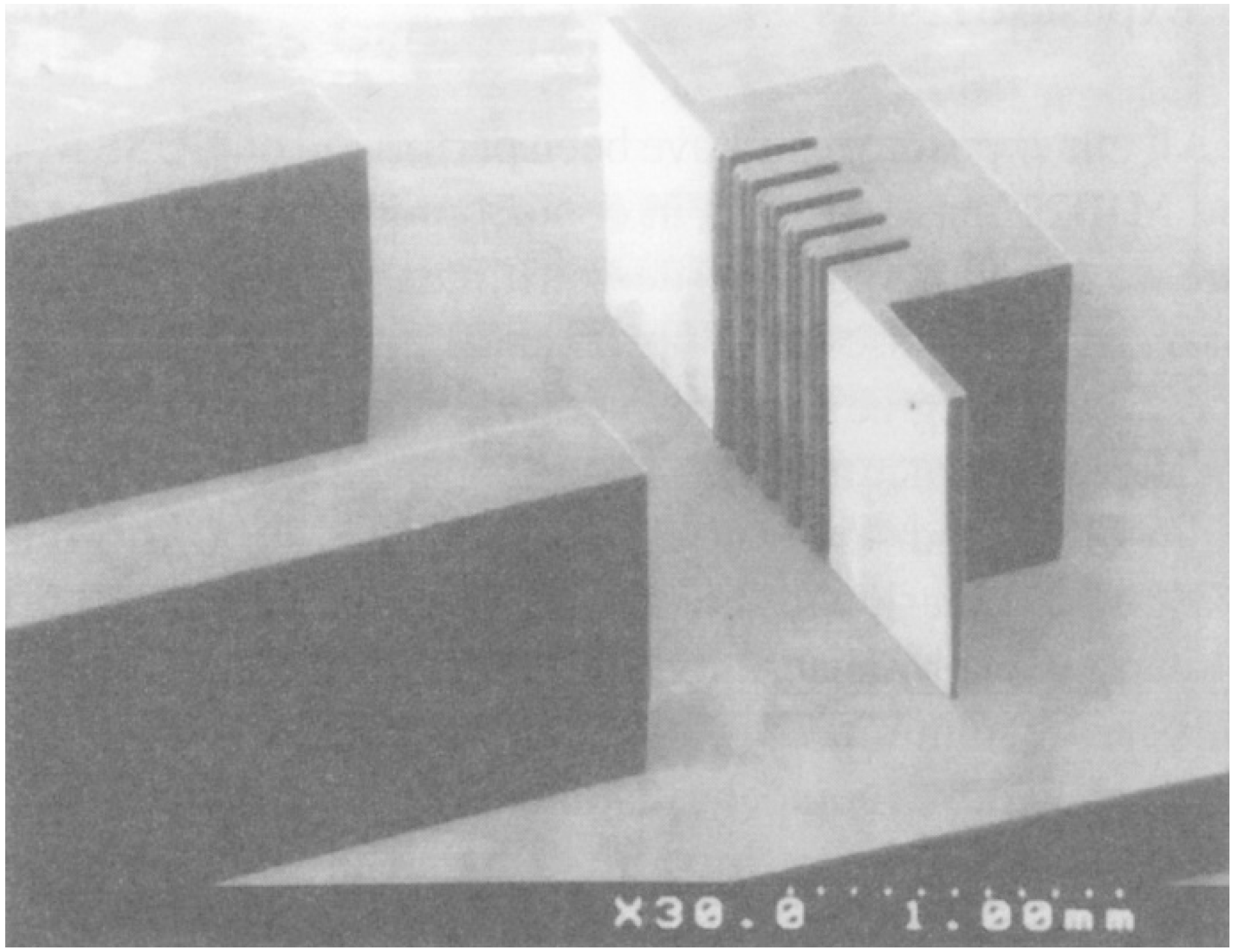
Figure 1.
SEM (scanning electron microscope) image of 1200 µm-thick structures in SU-8 with a linewidth of 65 µm, resulting in an aspect ratio of 18 (double-spin coated). From [6], © 1997 IEEE.
Figure 1.
SEM (scanning electron microscope) image of 1200 µm-thick structures in SU-8 with a linewidth of 65 µm, resulting in an aspect ratio of 18 (double-spin coated). From [6], © 1997 IEEE.

Beside bulk and surface micromachining techniques originally used for micromachining in the late 90s, LIGA can be considered a forerunner to additive manufacturing and a facilitator for the fabrication of micromechanical structures with a high degree of three dimensionality, or HARMS (high aspect ratio microstructures), desired for many applications.
2. SU-8 Microstructures
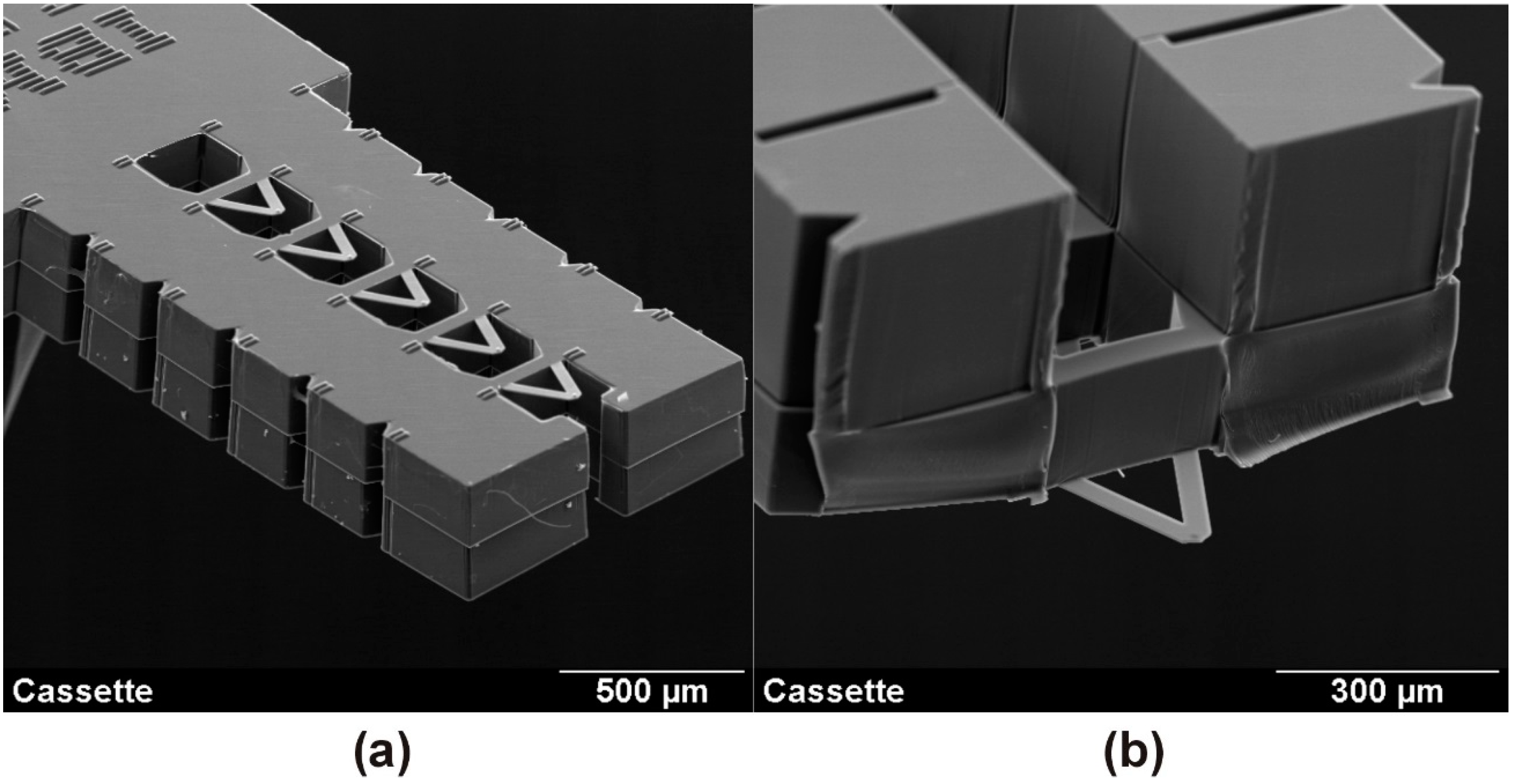
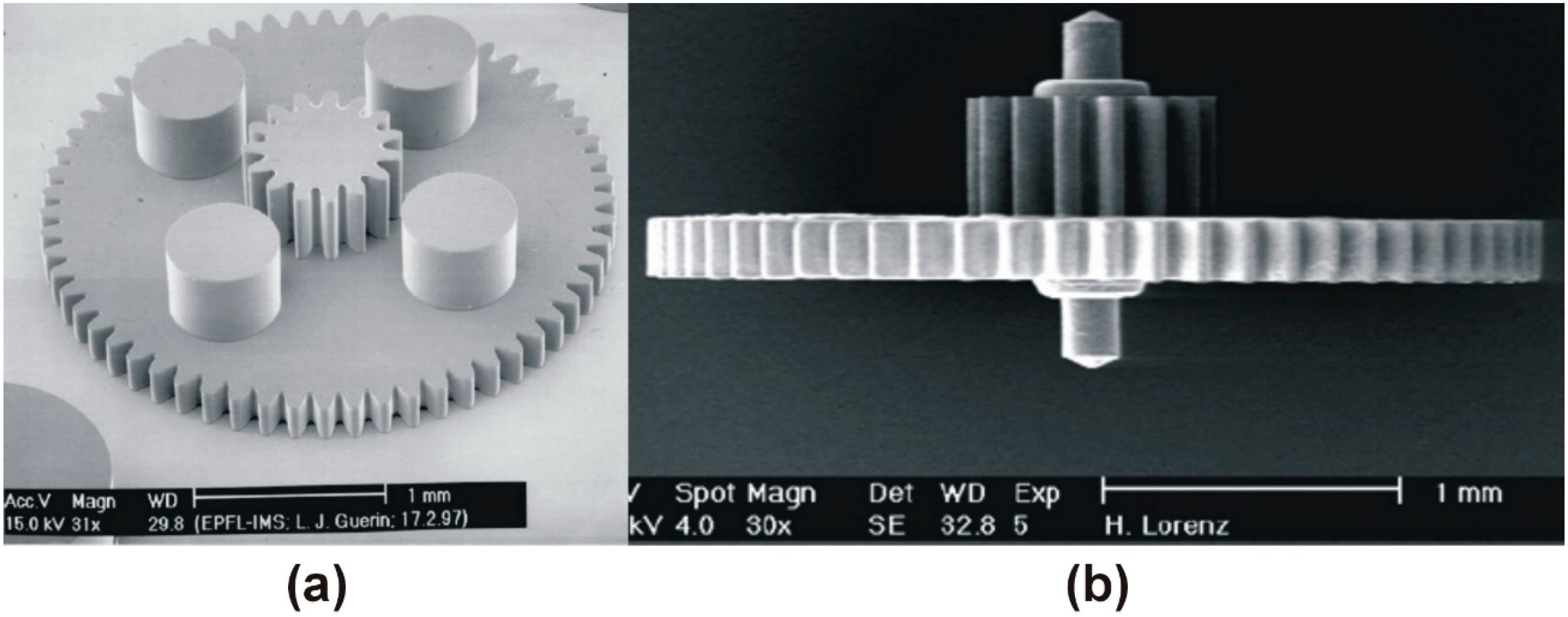
Due to its good mechanical, thermal and chemical stability, SU-8 turned out to be a very promising material for polymeric microstructures, also known as photoplastic parts. Low-cost micromechanical structures with micrometer and sub-micrometer features could be fabricated using this resist and standard photolithography steps. Near 3D microstructures could be batch fabricated on a wafer-scale, like micropumps, gearwheels [7] or microengines [8]. The low Young’s modulus of this material made it especially suitable for mechanical structures where low-stiffness parts were needed. Scanning probes for AFM (atomic force microscopy) or SNOM (scanning near-field optical microscopy) are good examples of possible applications brought by this photoplastic material [9]. Figure 2 shows an example where a complete cassette consisting of five different probes with pre-defined cut-off zones is entirely fabricated in SU-8 [10]. SU-8-based technology has established itself as an intermediate solution between the low-cost, high-volume fabrication provided by injection molding and the fine, controlled feature characteristics given by silicon technologies.
Figure 2.
(a) SU-8 cantilever cassette probe (shown tip-side up). The first lever is protected for ease of handling; (b) After breaking off the protective blocks, a cantilever is made ready for scanning. Trenches to facilitate the breaking off are clearly visible. Adapted from [10].
Figure 2.
(a) SU-8 cantilever cassette probe (shown tip-side up). The first lever is protected for ease of handling; (b) After breaking off the protective blocks, a cantilever is made ready for scanning. Trenches to facilitate the breaking off are clearly visible. Adapted from [10].

Direct use of SU-8 as a material has also been reported in numerous applications, like spacers for liquid crystal displays [11], waveguide and optical devices [12], micro-well arrays in microfluidic, dielectric material [13] or as a barrier layer in inkjet printing system [14], just to mention a few. The range of applications of SU-8 has reached such a great number that an exhaustive list is now far beyond the scope of this article.
3. Commercial Applications
3.1. Micromolds
The first real industrial applications using UV-LIGA technologies were developed in 1998 with the fabrication of micromold cavity inserts for injection molding. The advantages compared to traditional fabrication techniques, like wire electro discharge machining (WEDM), are very smooth sidewalls and the possibility to produce multi-layered auto-oriented cavities with sharp angles combining basic photolithographic steps and electroplating. Layer by layer, the epoxy photoresist is spin-coated onto a substrate, cured, exposed through a photomask and developed, resulting in a master built of SU-8 (Figure 3a). This master is then electroplated with nickel and destroyed. Afterwards, the resulting mold cavity is lapped down to a desired thickness and is ready to be used for micromolding plastic components (Figure 3b).
Figure 3.
(a) Two-level photoplastic SU-8 structure as a basis for micromold fabrication. From [6], © 1997 IEEE; (b) A micromolded multi-auto-oriented-level plastic polyoxymethylene (POM) component fabricated from an SU-8-based micromold.
Figure 3.
(a) Two-level photoplastic SU-8 structure as a basis for micromold fabrication. From [6], © 1997 IEEE; (b) A micromolded multi-auto-oriented-level plastic polyoxymethylene (POM) component fabricated from an SU-8-based micromold.

3.2. Microparts
Fabrication of metallic stand-alone parts without the idea of replication by injection molding was developed by a derivative process of LIGA. The structuration of the negative of the desired component into the photoresist and subsequent electroplating into this template resulted in the direct lateral definition of the parts. The microconnector, medical, pharmaceutical and biotechnology industries have a great need for components like mold inserts and microparts, but the watch industry has been shown to be the most receptive market for UV-LIGA.
3.3. Play-Free Engagement Gearing
In addition to a small sidewall roughness, the advantages given by the design freedom in the x-y plane enabled the fabrication of mechanical parts with integrated new functionalities. One of the most impressive examples of this characteristic has been shown with the manufacturing of gears with slotted teeth.
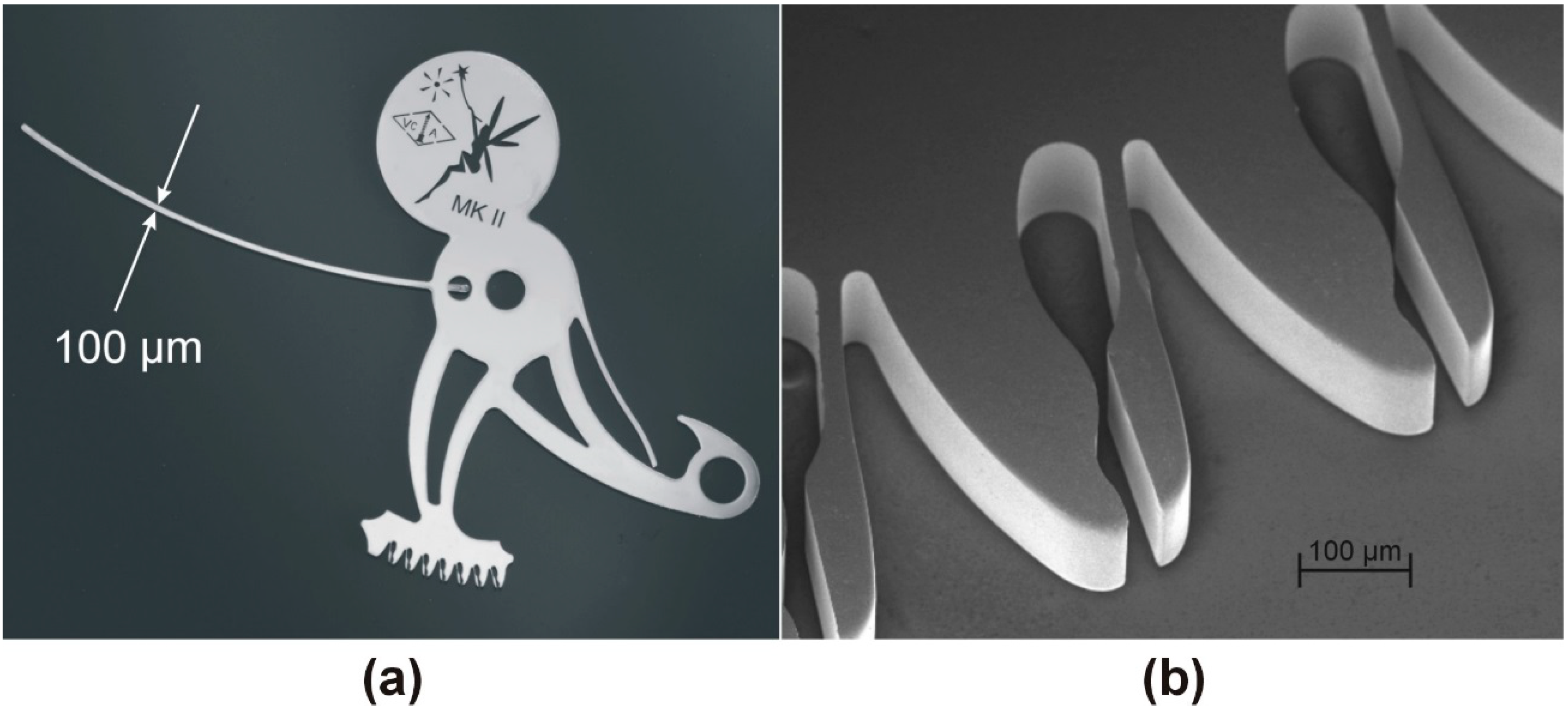
Developed by a Swiss watchmaker [15] inspired by the UV-LIGA technique, this invention [16] resulted in revolutionary improvements in mechanical watch movements. Thanks to unique design freedom brought by SU-8 photolithography, every tooth can be carved with an engineered shape in order to integrate a spring compensating any play in the gearing. First used in 2002, this play-free engagement system is now widely used in watches and delivers optimal transmission of force, a smooth display and more stability to the watch hands. Figure 4a shows a sector with different functions, like an identification number, an integrated logo, two spring blades and slotted teeth for play-free engagement. Figure 4b shows a close-up of the teeth. The part thickness is 120 µm, while the spring blade is 20 µm at its narrowest width.
Figure 4.
(a) Sector with identification number, integrated logo, springs and play-free engagement gearing; (b) SEM image of slotted-teeth. The spring part is 20 µm wide and 120 µm thick. Adapted from [17].
Figure 4.
(a) Sector with identification number, integrated logo, springs and play-free engagement gearing; (b) SEM image of slotted-teeth. The spring part is 20 µm wide and 120 µm thick. Adapted from [17].

3.4. Multi-Level Parts
The multiple photolithographic steps of SU-8 permitted the fabrication of multi-level parts. A single electroplating step on a multi-level mold obtains multi-level components. This solution reduces difficulties, uncertainties and failure risks brought by the subsequent assembly of sub-systems. Figure 5 shows a multi-level component fabricated in one electroplating in a multi-level resist template. A dart with a square foot and three auto-orientated levels have been electroplated in a three-level template.
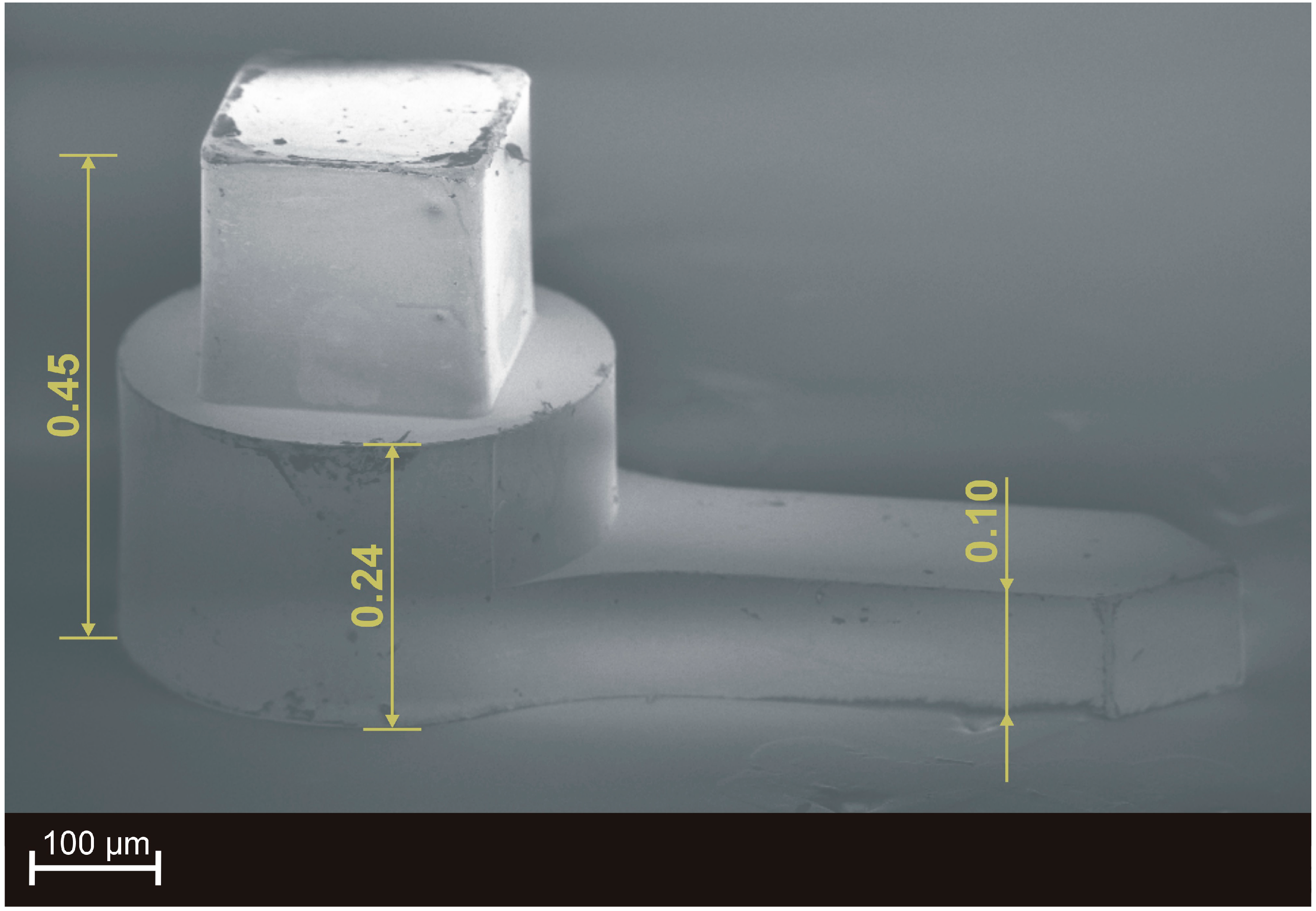
Figure 5.
SEM of a three-level dart. This part is shown upside-down, relating to its orientation during fabrication.
Figure 5.
SEM of a three-level dart. This part is shown upside-down, relating to its orientation during fabrication.

One advantage of using LIGA for fabricating mechanical elements is the excellent alignment between the different levels. This accuracy is a result of the alignment capabilities of mask alignment tools used during the photolithographic steps. Thanks to design freedom in the x-y plane, it is also possible to have levels with geometries difficult to obtain with standard machining techniques.
4. More than LIGA
4.1. Inserted Elements
Based on simple photolithographic steps, UV-LIGA has also shown a very high potential to be combined with other machining techniques. Insertion of single elements into the photoresist mold before electroplating enables fabrication of components with better functionalities [18]. This technique allows perfect positioning of the insert without any risk of damage during its fitting. The use of inserted elements in the watch industry or generally in microdevices gives the final part various advantages. A ruby can be inserted for tribological reasons or to avoid premature wear, for example. As rubies withstand any type of chemical products, inks or abrasive liquids, this makes them also ideal for nozzles.
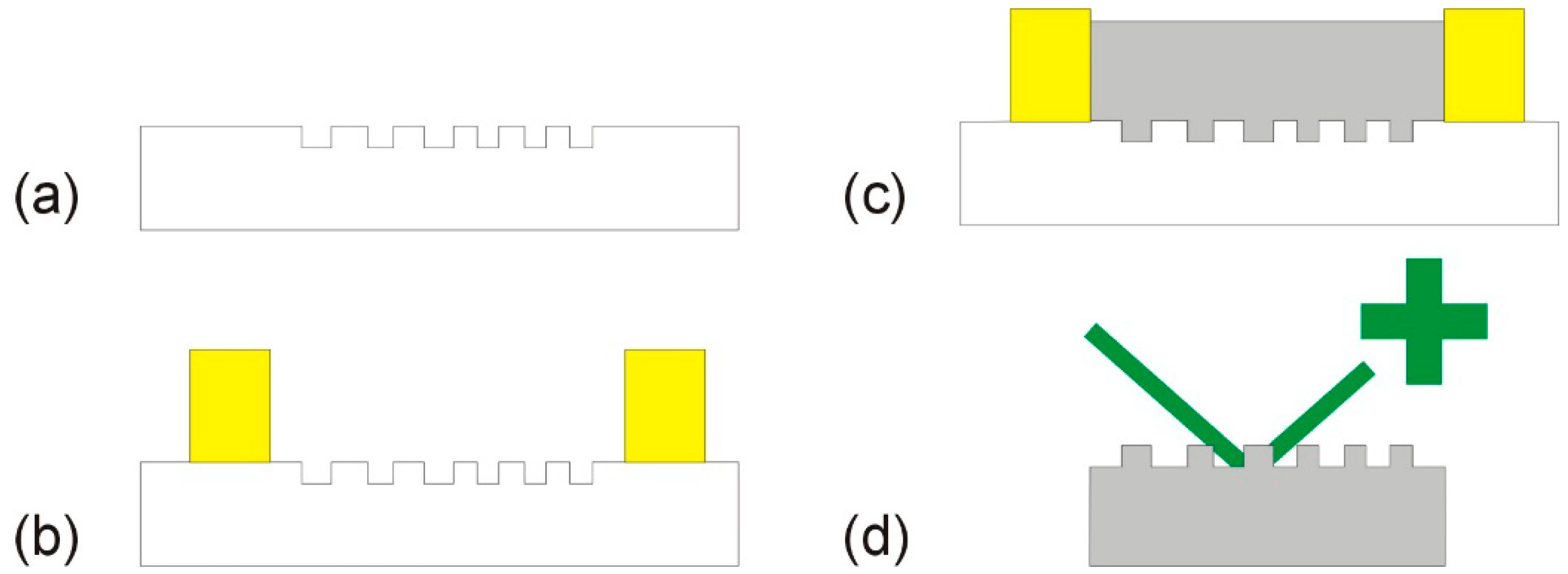
Figure 6 shows process steps for the fabrication of LIGA parts with integrated elements. A photoresist layer is spin-coated onto a substrate, cured, exposed and developed. This layer may define the final part, but may also be used in a multi-level process as a reference layer for the insert (Figure 6a). A part made with other manufacturing means is inserted into the photoresist template. Its well-defined position is given by the photolithography accuracy. This integrated element can be positioned by its key reference feature. This enables a decrease of the housing and integrated element tolerances (Figure 6b). Electroplating is done to fill the photoresist mold and the inserted element is then fastened by metal growth around its sidewalls (Figure 6c). Finally, after standard UV-LIGA steps, the metallic part with its inserted element is removed from the mold and substrate (Figure 6d).
Figure 6.
Process flow for the fabrication of parts with integrated elements using UV-LIGA technology: (a) SU-8 photoresist lithography for inserted element positioning and part template structuration; (b) positioning of inserted element; (c) electroplating in the photoresist template and around the inserted element; (d) removal of the substrate and photoresist to obtain the part with its integrated element.

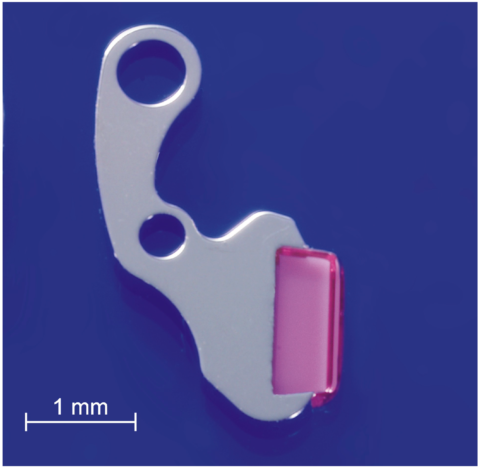
This fabrication technology is well adapted for fragile parts, as no driving forces are needed to assemble the different elements. Figure 7 shows an image of a LIGA part with an integrated ruby. Rubies are used in this case for their low friction coefficient and high hardness. Ruby positioning is given by its friction sidewall. Defined during the same photolithography step, the positioning of the rubies functional faces and the micropart holes are all in the micrometer range.
Figure 7.
Carrier lever with integrated ruby to reduce friction.

4.2. CLR-LIGA
Integration of a diffractive optical element (DOE) is another way of adding functionalization to a LIGA micropart [19]. Thanks to the very good replication properties of electroplating, it is possible to add nanometric features in functional micromechanical parts. Exposing a DOE segment with a coherent light displays an image. This technology has been called CLR-LIGA (covert laser readable-LIGA). Originally developed for authentication, such marking also serves for customization or tracking issues. The main advantage of using a DOE incorporated into a functional component for authentication is the insurance that the final product is real. Fabricating a mechanical part with a DOE combines standard micromachining technologies, like deep reactive ion etching (RIE) or KOH etching, for example, with UV-LIGA technology.
Figure 8 shows the process steps for the fabrication of LIGA parts with integrated diffractive optical elements. After calculation, a computer-generated diffractive pattern of an image is transferred into a substrate using wet or dry etching techniques or metal lift-off (Figure 8a). The standard LIGA process is then processed onto this pre-structured substrate, with photoresist spin-coating, curing, exposure and development (Figure 8b), followed by an electroplating step (Figure 8c). The part is released after removal of the photoresist and the substrate. The desired authenticator is revealed by covering the diffractive nanostructure with a laser (Figure 8d).
A critical step of this technology is the control of the etching thickness for DOE. This thickness is the main factor influencing diffraction efficiency.
Figure 9 shows SEM images of a functional LIGA part with a nanostructured diffractive optical element on one side. The depth of DOE is 130 nm, and the lateral resolution is 2 µm. The depth has been chosen to give optimal results with a standard green light laser pointer [20].
Figure 8.
Process flow for the fabrication of parts with an integrated diffractive optical element (DOE) using CLR-LIGA technology: (a) The nanostructuration of DOE onto the substrate using standard micromachining; (b) micromechanical part definition by SU-8 photolithography onto the pre-structured substrate; (c) electroplating in photoresist template and on DOE; (d) removing of the substrate and photoresist to obtain parts with integrated DOE.

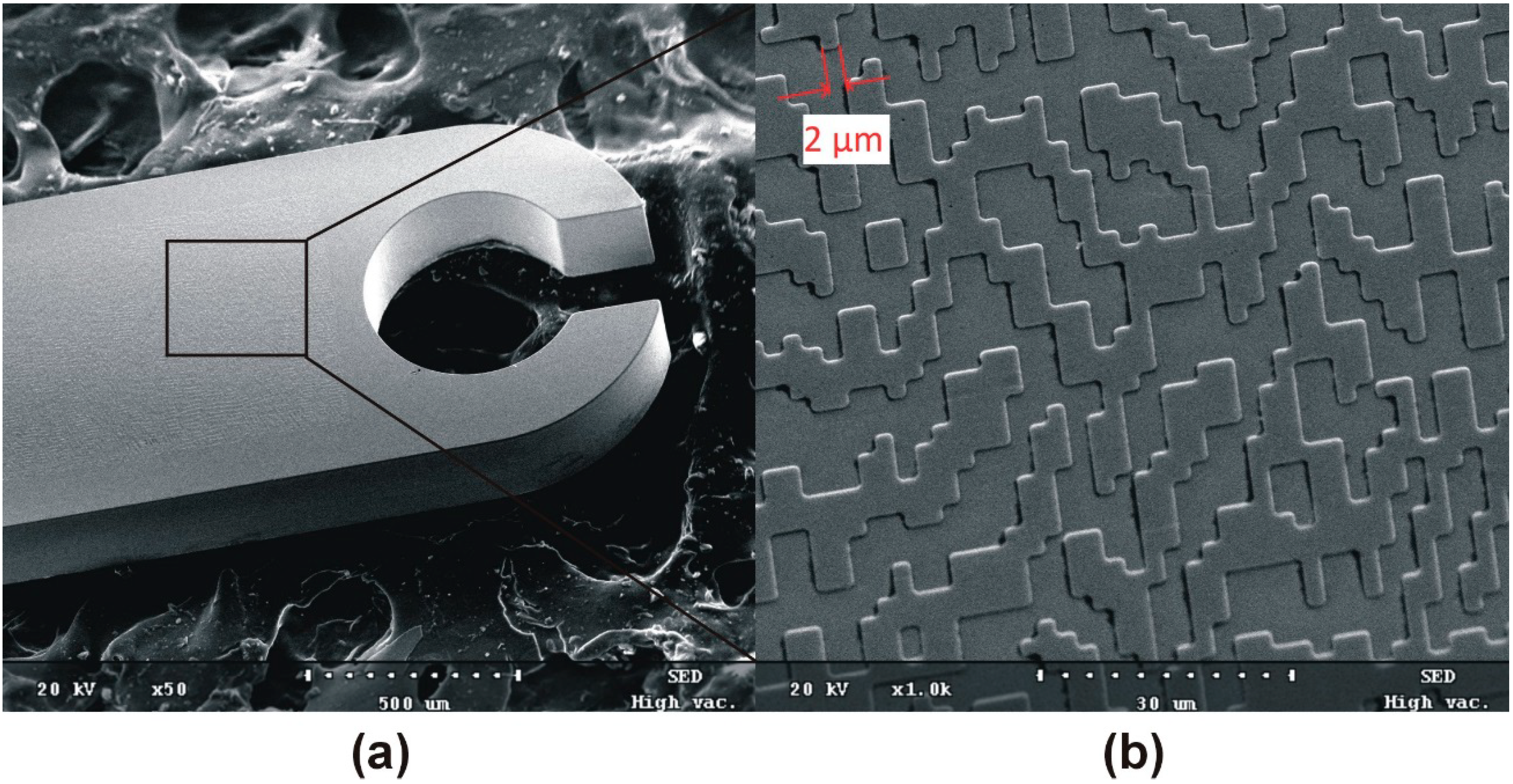
Figure 9.
SEM images of a LIGA part with a nanostructured DOE: (a) A 200 µm-thick functional microcomponent with an etched DOE; (b) a close-up of the nanostructured features. Pixels are 2 µm wide and 130 nm deep.
Figure 9.
SEM images of a LIGA part with a nanostructured DOE: (a) A 200 µm-thick functional microcomponent with an etched DOE; (b) a close-up of the nanostructured features. Pixels are 2 µm wide and 130 nm deep.

5. Conclusions
UV-LIGA has been shown to be well-adapted for the fabrication of mold inserts or microparts. However, innovation is a key element to keep this technology viable and competitive from an industrial and commercial point of view. The process evolution for introducing new functionalities and new features in the parts, process optimization for mass production and material development are some of the key issues that need to be continuously investigated to keep this technology as an alternative to the traditional machining of micro-components.
Author Contributions
Both authors contributed equally to this review.
Conflicts of Interest
The authors declare no conflict of interest.
References
- Becker, E.W.; Ehrfeld, W.; Münchmeyer, D.; Betz, H.; Heuberger, A.; Pongratz, S.; Glashauser, W.; Michel, H.J.; Siemens, R. Production of separation-nozzle systems for uranium enrichment by a combination of X-ray lithography and galvanoplastics. Naturwissenschaften 1982, 69, 520–523. [Google Scholar] [CrossRef]
- Saile, V.; Wallrabe, U.; Tabata, O.; Korvink, J.G. LIGA and Its Applications. In Advanced Micro & Nanosystems; Brand, O., Fedder, G.K., Hierold, C., Korvink, J.G., Tabata, O., Eds.; WILEY-VCH Verlag GmbH & Co. KGaA: Weinheim, Germany, 2009; Volume 7. [Google Scholar]
- Frazier, A.B.; Allen, M.G. Metallic microstructures fabricated using photosensitive polyimide electroplating molds. J. Microelectromech. Syst. 1993, 2, 87–94. [Google Scholar] [CrossRef]
- LaBianca, N.; Gelorme, J.D. High-Aspect-Ratio Resist for Thick-Film Applications. In Proceedings of SPIE 2438, Advances in Resist Technology and Processing XII, 846, Santa Clara, CA, USA, 9 June 1995.
- Lorenz, H.; Despont, M.; Fahrni, N.; LaBianca, N.; Vettiger, P.; Renaud, P. EPON SU-8: A Low-Cost Negative Resist for MEMS. In Proceedings of Micro Mechanics Europe, Barcelona, Spain, 21–22 October 1996; pp. 32–35.
- Despont, M.; Lorenz, H.; Fahrni, N.; Brugger, J.; Renaud, P.; Vettiger, P. High-Aspect-Ratio, Ultrathick, Negative-Tone Near-UV Photoresist for MEMS Applications. In Proceedings of the 10th IEEE International Workshop Micro Electro Mechanical Systems (MEMS’97), Nagoya, Japan, 26–30 January 1997; pp. 518–522.
- Seidemann, V.; Rabe, J.; Feldmann, M.; Buttgenbach, S. SU-8 micromechanical structures with in situ fabricated movable parts. Microsyst. Technol. 2002, 8, 348–350. [Google Scholar] [CrossRef]
- Peng, J.; Kyle, J.; Nianjun, S. Microfabrication of Ultra-Thick SU-8 Photoresist for Microengines. In Proceedings of SPIE 4979, Micromachining and Microfabrication Process Technology VIII, 105, San Jose, CA, USA, 25 January 2003.
- Genolet, G.; Despont, M.; Vettiger, P.; de Rooij, N. Sensors Update; Baltes, H., Hesse, J., Korvink, J.G., Eds.; WILEY-VCH Verlag GmbH: Weinheim, Germany, 2001; Volume 9, pp. 3–19. [Google Scholar]
- Genolet, G.; Despont, M.; Vettiger, P.; Anselmetti, D.; de Rooij, N.F. All-photoplastic, soft cantilever cassette probe for scanning force microscopy. J. Vac. Sci. Technol. B 2000, 3, 617–620. [Google Scholar] [CrossRef]
- Park, H.G.; Byun, S.U.; Jeong, H.C.; Lee, J.W.; Seo, D.S. Photoreactive spacer prepared using electrohydrodynamic printing for application in a liquid crystal device. ECS Solid State Lett. 2013, 2, R52–R54. [Google Scholar] [CrossRef]
- Borreman, A.; Musa, S.; Kok, A.A.M.; Diemeer, M.B.J.; Driessen, A. Fabrication of polymeric multimode waveguides and sevices in SU-8 photoresist using selective polymerization. In Proceedings of Symposium IEEE Lasers and Electro Optics Society (LEOS), Amsterdam, The Netherlands, 9 December 2002.
- MicroChem Corp. Website. Available online: http://www.microchem.com/Applications.htm (accessed on 26 May 2014).
- Lambright, T.M.; Selmeczy, A.; Lee, F.C.S.; Haluzak, C.C.; Trueba, K.E. Thermal inkjet print head with solvent resistance. U.S. Patent 8,454,149 B2, 28 June 2010. [Google Scholar]
- Agenhor Website. Available online: http://www.agenhor.ch (accessed on 26 May 2014).
- Wiederrecht, J.M. Gear for precision devices. WO Patent 2004/008004 A1, 27 May 2003. [Google Scholar]
- Genolet, G.; Lorenz, H.; Glassey, M.A. 10 ans de LIGA au service de l’horlogerie. Développements et nouveautés. In Nouveaux Matériaux et Innovations Technologiques en Horlogerie, Proceedings of the 12ème Journée d’Etude, Société Suisse de Chronométrie, La Chaux-de-Fonds, Switzerland, 17 September 2008. (In French)
- Lorenz, H.; Genolet, G.; Glassey, M.A. Mixed manufacturing method for parts by photolithography, adding inserts and electroforming. EP Patent 1916567 B1, 22 November 2006. [Google Scholar]
- Winkler, P. Pièces horlogères décorées avec des structures diffractives. Bulletin SSC (Société Suisse de Chronométrie) 2011, 66, 25–27. (In French) [Google Scholar]
- Mimotec SA Webpage. Available online: http://www.mimotec.ch/Anglais/Technology/technology.html (accessed on 26 May 2014).
© 2014 by the authors; licensee MDPI, Basel, Switzerland. This article is an open access article distributed under the terms and conditions of the Creative Commons Attribution license (http://creativecommons.org/licenses/by/3.0/).
Share and Cite
MDPI and ACS Style
Genolet, G.; Lorenz, H. UV-LIGA: From Development to Commercialization. Micromachines 2014, 5, 486-495. https://doi.org/10.3390/mi5030486
AMA Style
Genolet G, Lorenz H. UV-LIGA: From Development to Commercialization. Micromachines. 2014; 5(3):486-495. https://doi.org/10.3390/mi5030486
Chicago/Turabian StyleGenolet, Grégoire, and Hubert Lorenz. 2014. "UV-LIGA: From Development to Commercialization" Micromachines 5, no. 3: 486-495. https://doi.org/10.3390/mi5030486