Fabrication and Characterization of MoS2/h-BN and WS2/h-BN Heterostructures


1
Key Laboratory for Wide-Band Gap Semiconductor Materials and Devices of Education, School of Microelectronics, Xidian University, Xi’an 710071, China
2
State Grid Key Laboratory of Power Industrial Chip Design and Analysis Technology, Beijing Smart-Chip Microelectronics Technology Co., Ltd., Beijing 100192, China
*
Authors to whom correspondence should be addressed.
Micromachines 2020, 11(12), 1114; https://doi.org/10.3390/mi11121114
Submission received: 4 November 2020
/
Revised: 11 December 2020
/
Accepted: 13 December 2020
/
Published: 16 December 2020
(This article belongs to the Section D:Materials and Processing)
Abstract
:The general preparation method of large-area, continuous, uniform, and controllable vdW heterostructure materials is provided in this paper. To obtain the preparation of MoS2/h-BN and WS2/h-BN heterostructures, MoS2 and WS2 material are directly grown on the insulating h-BN substrate by atmospheric pressure chemical vapor deposition (APCVD) method, which does not require any intermediate transfer steps. The test characterization of MoS2/h-BN and WS2/h-BN vdW heterostructure materials can be accomplished by optical microscope, AFM, Raman and PL spectroscopy. The Raman peak signal of h-BN material is stronger when the h-BN film is thicker. Compared to the spectrum of MoS2 or WS2 material on SiO2/Si substrate, the Raman and PL spectrum peak positions of MoS2/h-BN heterostructure are blue-shifted, which is due to the presence of local strain, charged impurities and the vdW heterostructure interaction. Additionally, the PL spectrum of WS2 material shows the strong emission peak at 1.96 eV, while the full width half maximum (FWHM) is only 56 meV. The sharp emission peak indicates that WS2/h-BN heterostructure material has the high crystallinity and clean interface. In addition, the peak position and shape of IPM mode characteristic peak are not obvious, which can be explained by the Van der Waals interaction of WS2/h-BN heterostructure. From the above experimental results, the preparation method of heterostructure material is efficient and scalable, which can provide the important support for the subsequent application of TMDs/h-BN heterostructure in nanoelectronics and optoelectronics.
1. Introduction
The two-dimensional van der Waals (2D vdWs) heterostructure materials have attracted research interest from researchers, and the controlled stacking of different 2D materials would greatly expand the type and application of heterostructures, which is due to the unique planar structure, excellent electrical and optical properties [1,2]. As the representative transition metal dichalcogenides (TMDs) materials, MoS2 and WS2 materials show the direct optical band gap, which has the significant photoluminescence (PL) intensity [3]. The band gap and dielectric constant of hexagonal boron nitride (h-BN) material, respectively, are 6 eV and 4, which has the excellent physical characteristics and atomic surface flatness [4]. For the inherent properties exploration of atomic layer materials, h-BN material is used as the most suitable substrate, and the performance can be improved when TMDs materials are stacked on the insulating h-BN substrate. Besides, the clean and flat heterojunction interface with the low-density charged impurities and dangling bonds can be formed [5,6]. The TMDs/h-BN vertical heterostructure materials can provide the unique platform, which can explore the unique phenomena of condensed state physical and electrical properties [7,8]. Based on the vdW interlayer coupling interaction, various vdW heterostructures exhibit unique quantum phenomena, which can be widely used in field effect transistors [9], sensors [10,11] and photodetectors [12].
There are many unexplored problems in the interlayer coupling of TMDs/h-BN heterostructures, and it is necessary to have a better understanding and application of vdW heterostructure [13,14]. The heterostructure combination of any layered materials can be prepared by transfer method, so the devices with new functions and characteristics are also realized by combining the different characteristics materials [15,16]. For the mass production of heterostructure materials, the mechanical peeling stack method is not suitable, due to the lower yield [17]. During the transfer processes, it can introduce the impurity contamination at the interface between h-BN and Graphene, and it can be severely limited by the interfacial contamination, poor interlayer contact and insufficient production scale, which would decrease the interlayer interaction [18,19,20]. Additionally, the method has a great impact on the properties of heterostructures. It is a more scalable and controllable method when 2D layered materials directly grown on another layer of material, which can produce the clean interface [21,22]. During the preparation of vdW heterostructure, 2D h-BN material has the flat surface and charge uniformity, it can achieve a cleaner interface, which is a good ideal insulating substrate [23,24,25]. The large area, continuous, uniform, and controllable preparation of TMDs/h-BN heterostructure is still a huge challenge. Therefore, it is necessary to develop a general construction method, which can use the same preparation processes to arbitrarily stack high-quality layered materials.
The research mainly includes the following parts. First, the h-BN material on Pt substrate is prepared by CVD method, which is transferred to SiO2/Si substrate. To confirm the existence of h-BN material, the spectral characteristics of h-BN materials with different layers are then tested and analyzed, which can provide a good foundation for the preparation of heterostructures. Next, MoS2 and WS2 materials are directly grown on the insulating h-BN substrate by APCVD method, which can complete the preparation of MoS2/h-BN and WS2/h-BN hetero-structures. Subsequently, the test characterization of MoS2/h-BN and WS2/h-BN vdW heterostructure materials can be accomplished by optical microscope, AFM, Raman and PL spectroscopy. Finally, the above characteristics would facilitate the preparation of TMDs/h-BN vdW heterostructure, which would also promote the application of TMDs/h-BN heterostructures in the next-generation optoelectronic devices, flexible electronics, and optoelectronics [26,27].
2. The Controlled Growth Preparation Experiment and Transfer of h-BN
The platinum (Pt) sheet with a thickness of 20 µm and a purity of 99.95% is selected in the growth experiment of h-BN. This is because Pt substrate has the smooth atomic surface, which is conducive to the growth of high-quality, uniform h-BN thin film [28]. Besides, Pt substrate can also be reused by using the bubble transfer method. The following describes cleaning processes of Pt substrate. First, Pt sheet is cut to a size of 1.5 × l cm. Then, these Pt sheets are put successively in the acetone and alcohol solution for the ultrasonic cleaning of 10 min, which can remove organic matter and impurities on the surface of Pt sheets. Finally, Pt sheets are blown dry with nitrogen gas.
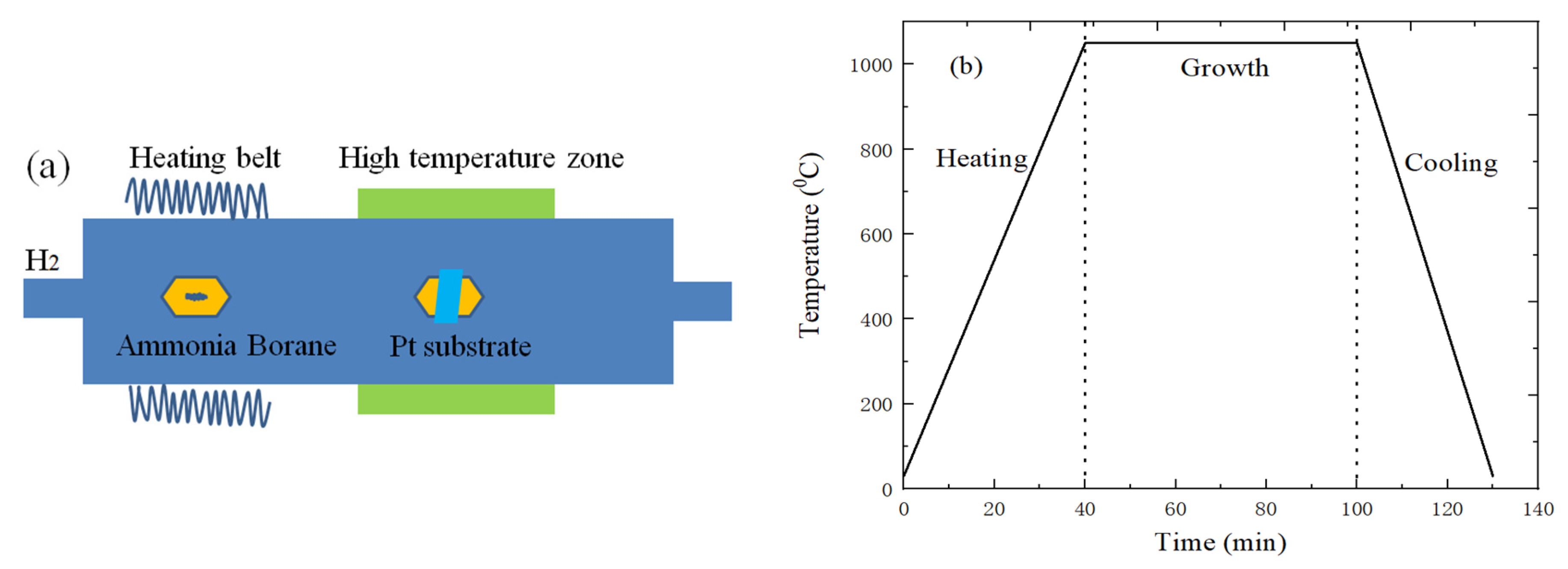
Figure 1a is the growth schematic diagram of h-BN on Pt substrate by CVD method. The ammonia borane precursor powder is heated by heating belt, and it can generate Hydrogen gas (H2), Aminoborane Polymer and Borazine [29]. As a solid material, aminoborane polymer remains in the quartz boat, and Borazane enters the high temperature heating zone of furnace under H2 gas. Meanwhile, Borazane can be dehydrogenated again under the catalytic action of Pt, so the B and N atoms combine to form h-BN. The preparation of h-BN would be affected by the precursor ammonia borane powder amount, heated temperature and growth time [30]. The h-BN film with different sizes, morphologies and nucleation density can be prepared by changing growth conditions.
The ammonia borane powder is, respectively, placed and wrapped in a U-shaped quartz boat and copper foil, and it is placed on the intake side in the air flow direction, which can decrease the amount of aminoborane polymer particles deposited on the surface of Pt substrate. At the same time, the open quartz boat with cleaned Pt substrate is placed in the high temperature heating zone of the CVD system. The following describe the specific growth processes of h-BN. The heating zone of the CVD tube furnace is first heated to 1050 °C, and Pt substrate is annealed and recrystallized for 30 min. Next, the ammonia borane powder can be heated by the heating belt. When entering the growth stage of h-BN, it is necessary to maintain the appropriate amount of H2; the specific growth temperature changes of h-BN are shown in Figure 1b. Finally, the heating belt and furnace power supply need to be quickly cut off when the growth of h-BN is over, and enter the cooling stage.
The following are the specific transfer processes of h-BN material [31]. First, PMMA polymer with 3% mass score is suspended successively on the surface of h-BN/Pt substrate in the rotating speed with 500 rpm of 10 s and 1500 rpm of 20 s, and the h-BN with PMMA polymer is put on the heating table at 100 °C for 5 min, which can cure the PMMA polymer. Then, the PMMA/h-BN/Pt sample is immersed in the aqua regia solution (1 mol/L) for 1 h, and PMMA/h-BN would float on the surface of solution when Pt substrate is etched. Next, PMMA/h-BN sample is fished in deionized water and allowed to stand for 30 min, and the operation is repeated three times to clean h-BN. Subsequently, PMMA/h-BN is picked up with SiO2/Si substrate, and the sample is placed on hot plate. It is heated at 60 °C to remove the water between PMMA/h-BN and SiO2/Si substrate, which would promote h-BN material and SiO2/Si substrate combined closely. Afterwards, PMMA/h-BN/SiO2/Si sample is immersed in acetone solution for 30 min, then the acetone solution is replaced and allowed to stand for 12 h, before the h-BN/SiO2/Si sample is blown dry with nitrogen gas. Finally, h-BN/SiO2/Si sample is annealed at 400 °C for 1 h, which removes the PMMA polymer, water and other impurities on the surface of h-BN.
3. The Preparation and Characterization of TMDs/h-BN Heterostructure
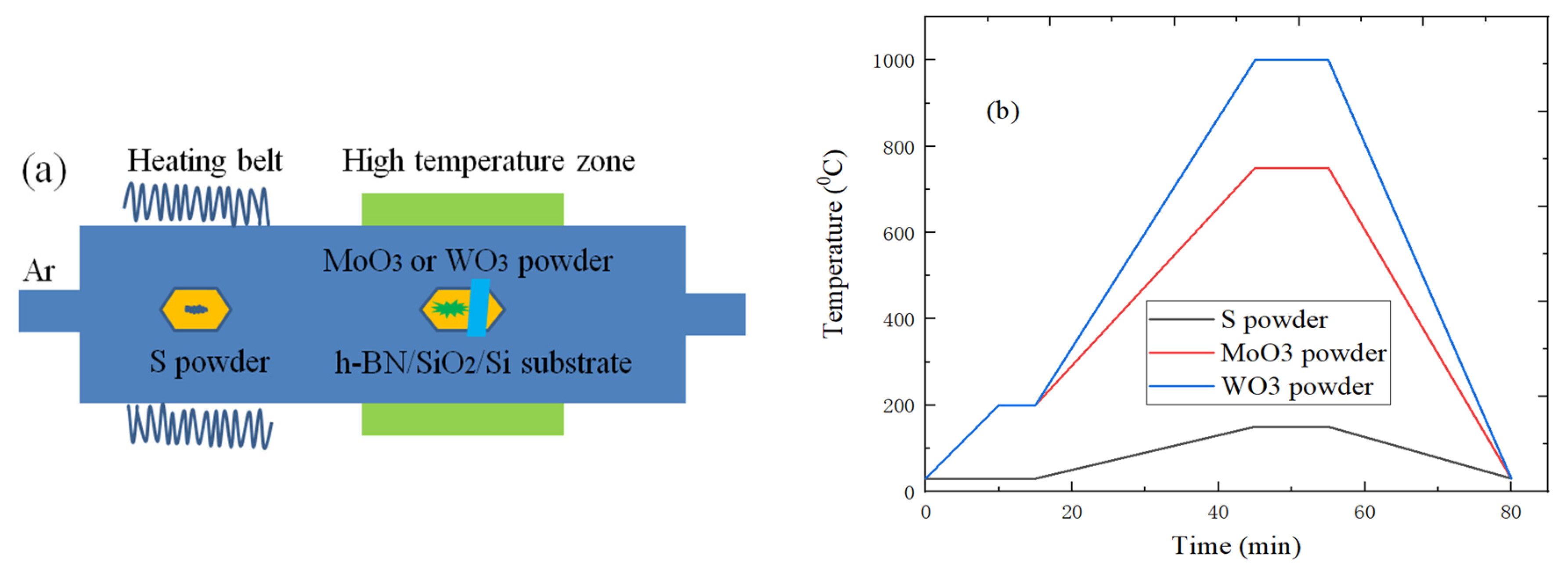
Figure 2a shows the preparation schematic diagram of TMDs/h-BN heterostructure, which can be achieved by using APCVD method to grow MoS2 and WS2 on h-BN/SiO2/Si substrate. The S powder, WO3 or MoO3 powder are, respectively, put into two quartz boats, h-BN/SiO2/Si substrate is placed on the top of quartz boat with WO3 (or MoO3) powder, and the above quartz boats are sent to the corresponding position of tube furnace, wherein the quartz boats with 100 mg S powder and 2 mg WO3 (or MoO3) powder are, respectively, placed in the area 1 and area 2, as show in Figure 2a. Additionally, the high-purity argon gas is used as carrier gas during the growth process. In Figure 2b, each temperature zone of the CVD system is set to the corresponding reactants temperature, the temperature of S powder is set to 150 °C, and the WO3 or MoO3 powders are 1000 °C and 750 °C, respectively. It is necessary to continuously provide 300 sccm Ar gas for 20 min before heating to exhaust the air and purify CVD growth system. Subsequently, the flow rate of Ar gas is adjusted to 50 sccm, and the growth time is maintained for 10 min. The S powder would evaporate and react with the MoO3 or WO3 powders during the growth processes. The competitive processes of sublimation, reaction, transfer, diffusion and precipitation can be balanced, which is beneficial to the dense growth of WS2 and MoS2 materials. When the chemical reaction is over, the system can naturally cool to room temperature. At the same time, it is necessary to continue to provide Ar gas to eliminate the residual gas of tube furnace. The temperature of S powder, WO3 or MoO3 powders can be separately controlled by tube furnace, and the supply rate of reactants can also be controlled by furnace temperature. In order to stably provide the optimal rate for each reactant material, it is crucial to independently control the supply rate and growth temperature. The TMDs material growth is completed under the optimal conditions, which would improve the operability of the reaction process.
The morphology and size of WS2/h-BN and MoS2/h-BN heterostructure materials (SixCarbon Technology Shenzhen, Shenzhen, China) can be observed and measured by the optical microscope, Atomic force microscopy (AFM), Raman and photoluminescence (PL) spectroscopy, which can study the structure, film thickness, internal and external strains of TMDs/h-BN heterostructures [32]. The Raman and PL spectroscopy analysis are carried out with the high-resolution dispersion Raman spectrometer, and the corresponding test condition is under the 532 nm laser with a spatial resolution of 1 µm. The horizontal and vertical spatial resolution is 1 and 2 µm, respectively. The 100× objective lens is used to focus the laser beam onto the TMDs/h-BN heterostructure in this experiment, and scattered light can also be collected by the objective lens. The excitation power is less than 1 mW, and the laser power is adjusted from 0.1% to 100% continuously and automatically, which can achieve the accurate measurement of Raman and PL spectrum. The notch filter is used to filter out the Rayleigh radiation, and the charge-coupled device (CCD) is also used to detect Raman and PL signals. The focal length, scanning speed, Raman filter, and the lowest wave number are 800 mm, 3 µs/pixel, 50 cm−1 and 10 cm−1. The Raman measurement range is 0–1500 cm−1, and the photoluminescence spectrum measurement range is 550–800 nm. All optical characterizations are carried out under the normal pressure and temperature.
4. The Characterization of MoS2/h-BN Heterostructure
4.1. The Optical Micrograph of MoS2/h-BN Heterostructure
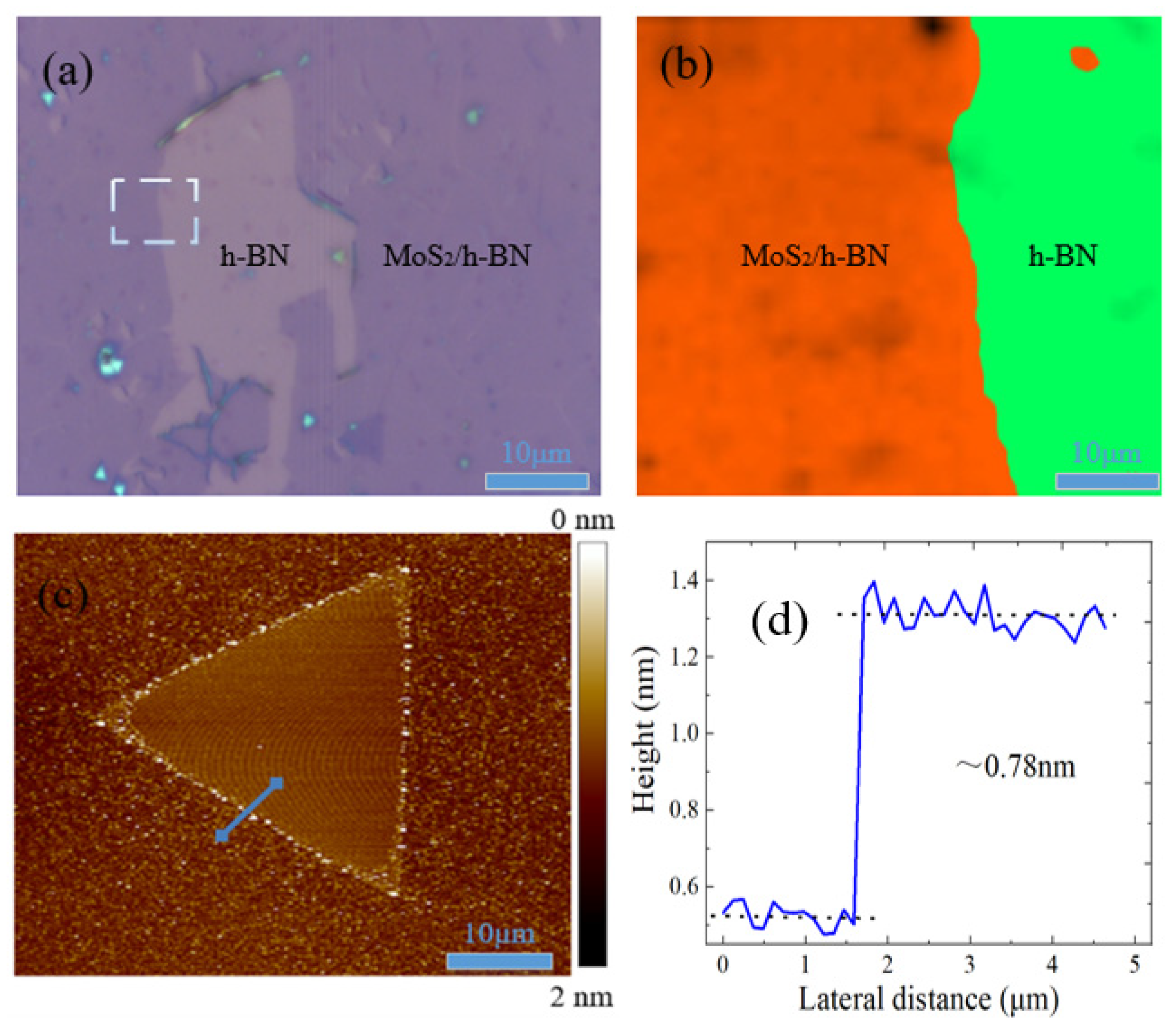
Although the lattice constants of two materials are highly mismatched, the vdW epitaxy technology can still cause one type of 2D material to grow on another material through the rotationally proportional manner, which can form the TMDs/h-BN heterostructure materials with oriented lattice match. Figure 3 shows the optical microscope images of MoS2/h-BN heterostructure on SiO2/Si substrate at different position. The growth mode of MoS2 on h-BN is Frank Van der Merwe mechanism, and MoS2 would first form a small 2D nucleus and then grow into the large 2D crystal. In addition, the clean and smooth surface of h-BN is suitable to the CVD growth of single crystal MoS2, and it can determine the crystal orientation, which is conducive to form the continuous film. Additionally, the low relative rotation angle between MoS2 and h-BN can be attributed to vdW epitaxy, which can be affected by the Coulomb interaction and vdWs force. Figure 3b is the Raman spectrum mapping of MoS2/h-BN heterojunction; there are few defects, the fluorescence efficiency is very high, and the quality and uniformity of heterojunction sample are very uniform and good, respectively. Besides, AFM is the most commonly used test method to characterize the thickness of nanomaterials. It can be found by observing Figure 3c,d that the height difference between the sample surface of MoS2 material and the surface of h-BN/SiO2/Si substrate is 0.78 nm, which can be judged as the monolayer MoS2 material.
4.2. The Spectral Characteristics of h-BN on SiO2/Si Substrate
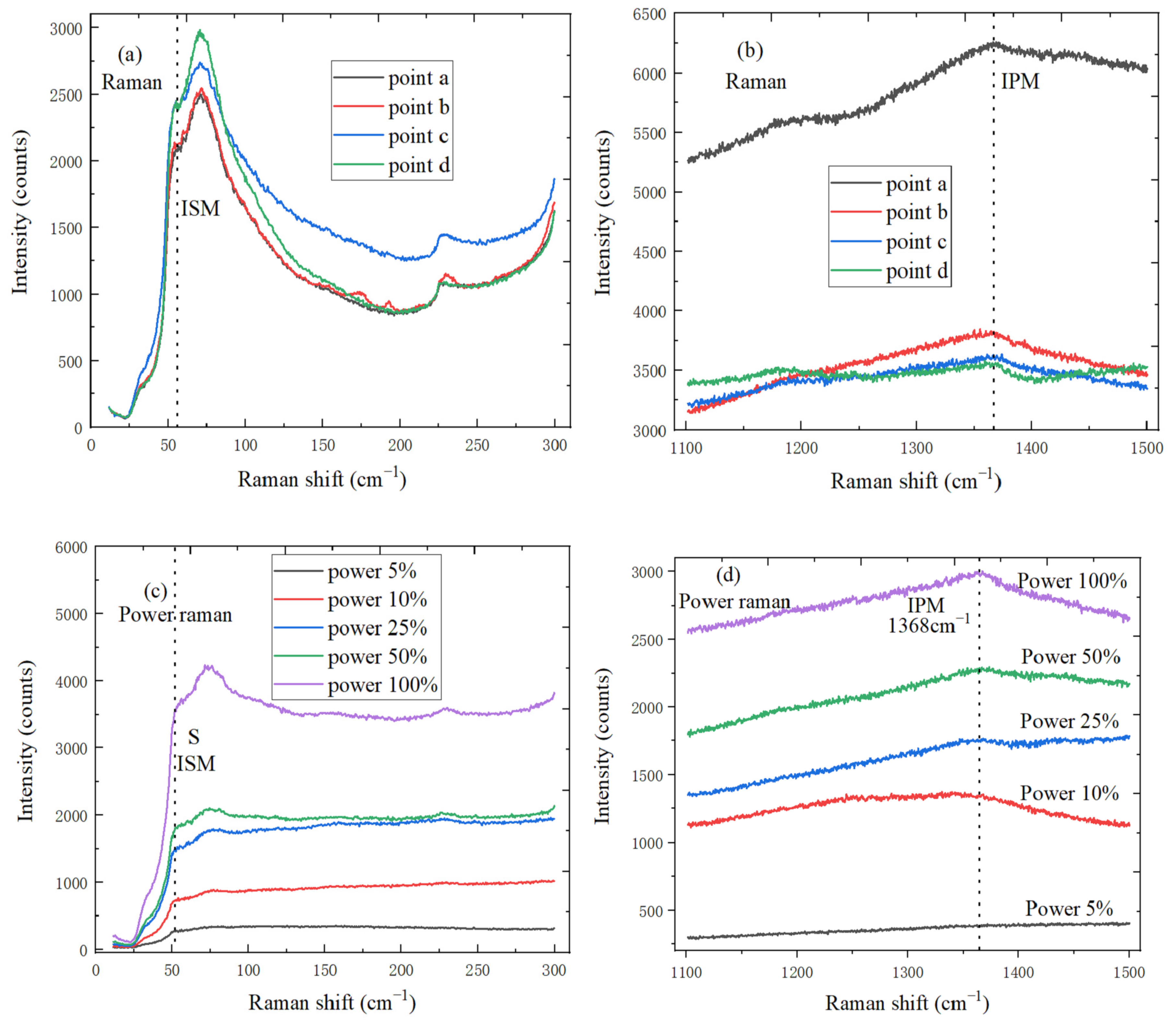
Raman spectroscopy is used to characterize and analyze the transferred h-BN material; points a, b, c, and d in Figure 4a,b are selected from the different h-BN material regions on SiO2/Si substrate, the ultra-low frequency line at 54.5 cm−1 and the high-frequency line at 1361 cm−1, respectively, correspond to the interlayer shear mode (ISM) with E2g symmetry and in-plane mode (IPM). Since both modes belong to the same irreducible representation, the huge difference of intensity is interpreted as Raman tensor, and crystallinity of the transferred h-BN is very high, which is the energy difference sign between weak interlayer interaction and atomic interaction of the strong plane [33]. The peak position of ISM mode change with the laser power increases, as show in Figure 4c. In the thinner h-BN sheet, the thermal effect is more obvious. When the higher laser power is used on the h-BN sample, the temperature would rise, and the peak position would cause the additional frequency shift. In addition, Raman process of h-BN is non-resonant when the laser source is in visible range. The ISM Raman signal of nanoscale layer hBN is much weaker than that of other 2D materials, so the longer integration time need be required to minimize the noise level. In Figure 4d, the temperature around h-BN sample increases with laser power increases, IPM frequency changes linearly with temperature, and the IPM mode peak intensity also increases. The reason is that phonon–phonon interaction can generate the non-harmonicity, peak position of IPM mode is more temperature dependent, and IPM mode frequency is more sensitive to the sample heating.
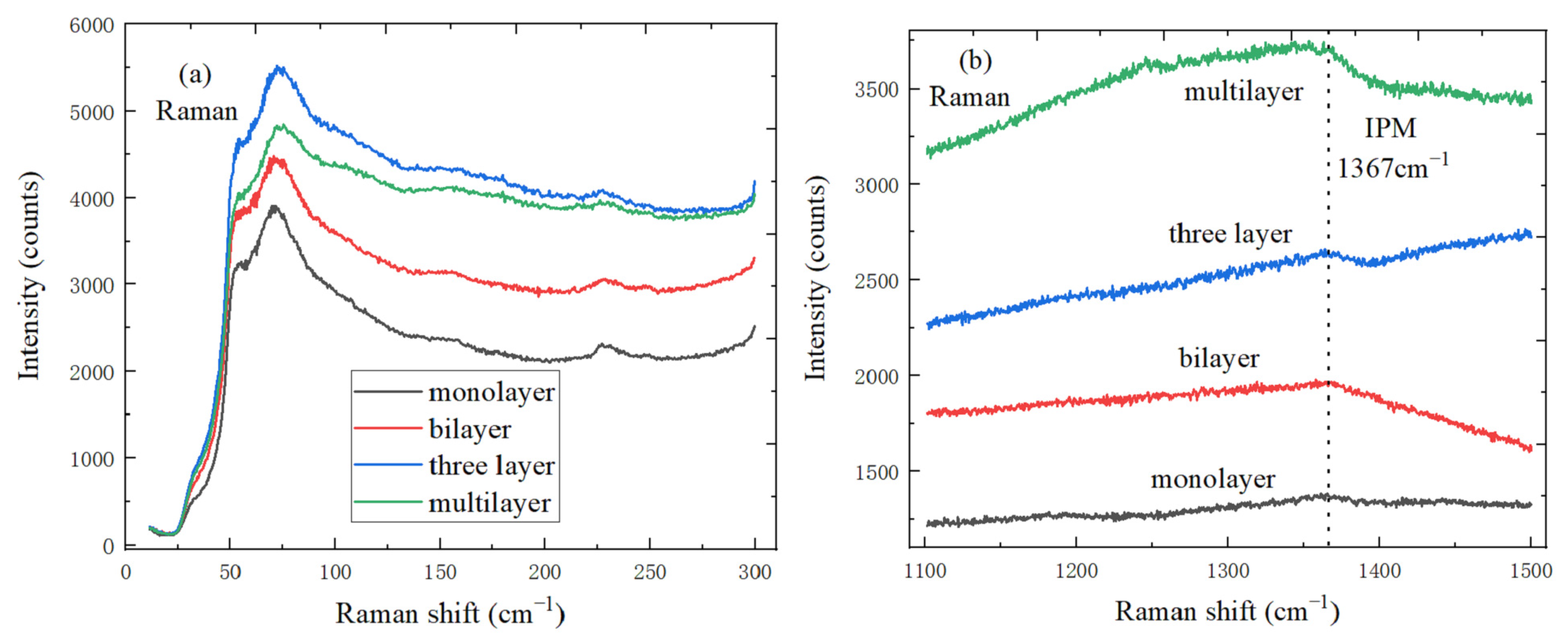
4.3. The Spectral Characteristics of h-BN with Different Layers on SiO2/Si Substrate
Figure 5a plots the group Raman spectrum of h-BN samples from monolayer to multi-layer, the Stokes spectrum is also plotted in low frequency region, and peak position of ISM shear mode would strongly move down when the thickness decrease. In Figure 5b, the peak position of IPM mode characteristic peak is at 1367 cm−1, IPM frequency shift does not change significantly with the layer number, and Raman signal is stronger when h-BN film is thicker [34].
4.4. The Spectral Characteristics of MoS2 on SiO2/Si Substrate
The Raman and PL spectroscopy are used to analyze the physical properties of MoS2, and PL emission spectroscopy is a powerful tool for studying the energy band structure and electronic excitation. The neutral excitons can be generated by the Coulomb interaction between an electron and a hole, and the excitons are charged by combining another electron or hole. The Raman and PL spectrum phenomena are largely dependent on temperature, which can lead to the thermal expansion/contraction of lattice and anharmonic interaction between phonon modes.
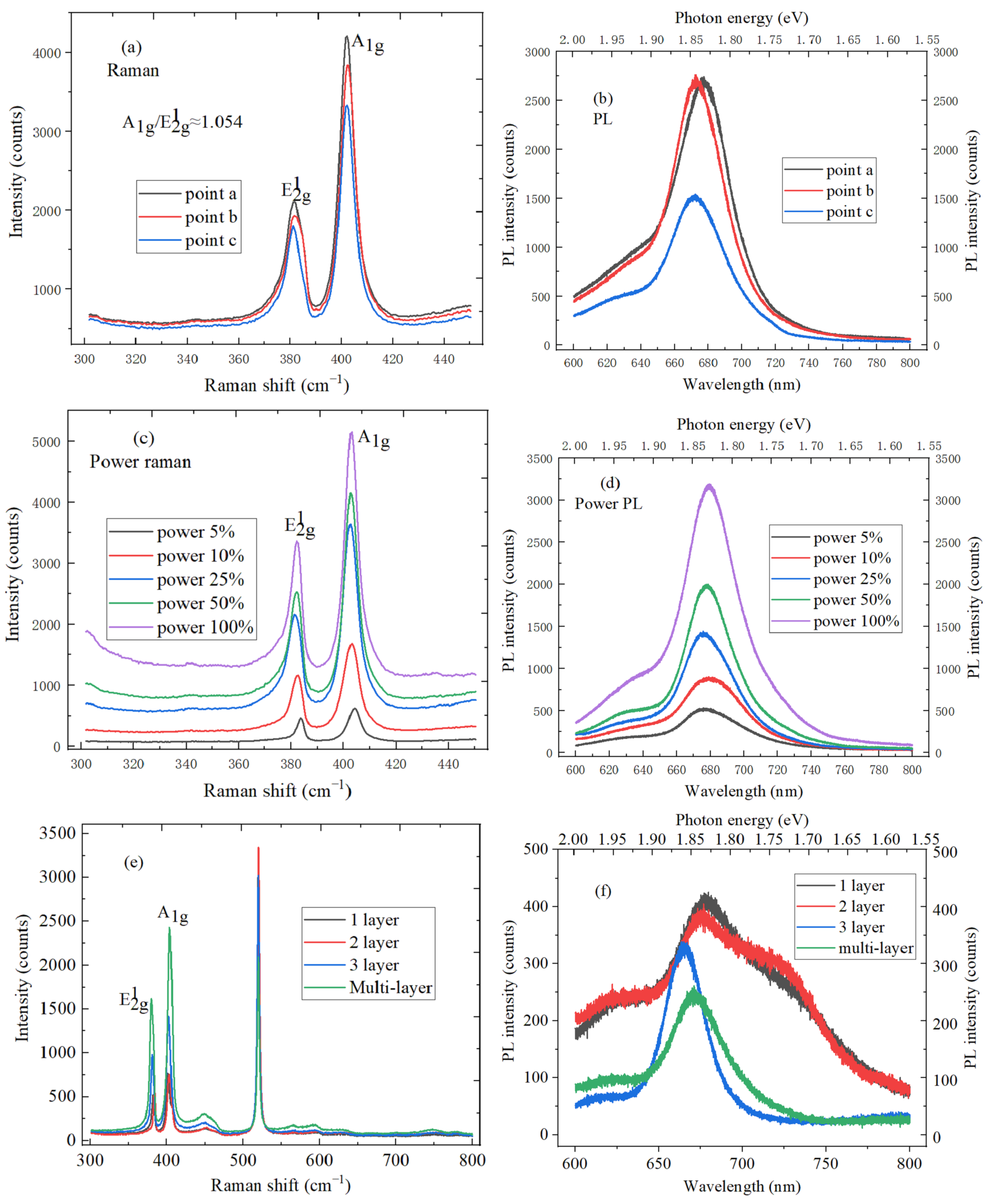
The Raman peak of silicon is located at 520 cm−1 under 532 nm excitation wavelength at the room temperature, and Raman peak frequency of silicon represents the actual temperature, which can calibrate the spectrums. The Raman and PL spectroscopy tests were performed at the three different test points of MoS2 material on SiO2/Si substrate. In Figure 6a, E12g and A1g mode characteristic peaks can be observed under the non-resonant condition of 532 nm laser, the in-plane E12g mode comes from the opposite vibration of Mo atoms relative to two S atoms, while Alg mode participates in the out-of-plane vibration of S atoms in opposite directions. The layer dependence between E12g and A1g mode characteristic peaks is mainly due to the long-term Coulomb interaction and the interlayer vdW force. The E12g and A1g mode characteristic peaks are, respectively, located at 381.7 and 400.3 cm−1, the distance is 18.6 cm−1, and the ratio of A1g/E12g is about 1.05, which indicates the existence of monolayer MoS2. It can be found by observing Figure 6b that PL spectrum is fitted by the Lorentz function, the peak position of the strongest PL intensity is located at 672.2 nm, and the corresponding band gap width is 1.85 eV, which is consistent with the direct band gap of monolayer MoS2. Monolayer MoS2 material shows the direct electron band gap of 1.85 eV, multi-layer MoS2 is the smaller indirect gap material, and the transition can greatly improve the quantum yield of PL spectrum. Figure 6c is the power Raman spectrum of MoS2, the peak intensity of the Raman spectrum gradually increases with the laser power increases, and E12g and A1g mode characteristic peak positions are the blue-shifted. The reason is that the temperature change of MoS2 would cause the non-harmonic interaction between phonon modes, thermal expansion and the contraction of lattice when the laser power increases. As the electron-phonon coupling increases, PL peak energy appears the red-shifted with temperature increases, as shown in Figure 6d. Additionally, PL spectrum intensity increases with the laser power increases. The resonance Raman scattering of MoS2 is studied by matching the excitation energy to PL spectrum exciton peak energy of MoS2, which can help to understand and master the energy band structure and exciton transition. Figure 6e shows the Raman spectrum of MoS2 material with different layers, the peak spacing between E12g and A1g characteristic peaks increases with the layer number of MoS2 material increases, which can be used to judge the layer number of the MoS2 material. It can be found by observing Figure 6f that the characteristic peak intensity decreases with the layers number of the MoS2 material increases. The direct gap upper limit of MoS2 material is 1.87 eV under our experimental conditions, and the peak position of I characteristic peak has a red shift to a certain extent with the layer number decreases, which can be explained by the vdWs interaction force.
4.5. The Spectral Characteristics of MoS2/h-BN Heterostructure on SiO2/Si Substrate
The Raman and PL spectroscopy are used to explore the lattice strain effects, doping levels and the stacking interactions of heterostructure, which can estimate the quality of MoS2/h-BN heterostructure material. Furthermore, measurement results can be analyzed and compared with that of monolayer MoS2 grown on SiO2/Si substrate by CVD.
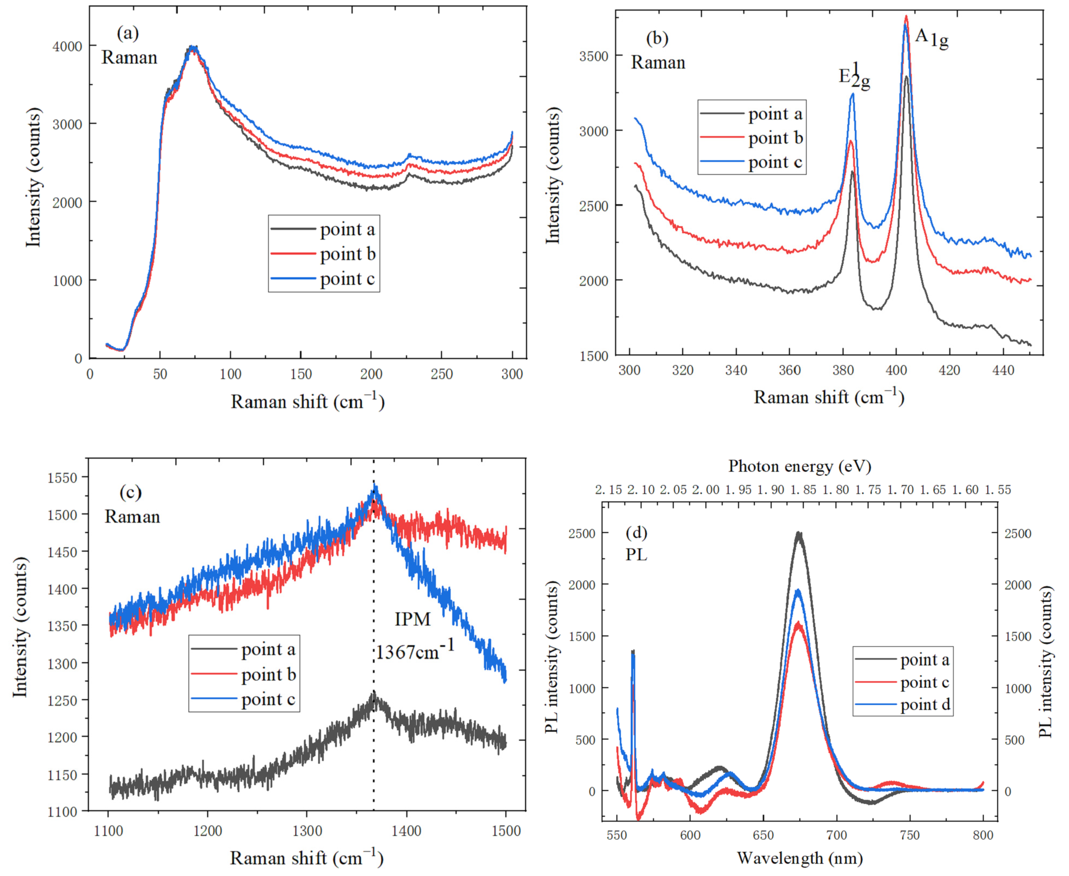
Figure 7a shows the ISM mode peak of h-BN at three different test points in the CVD-grown MoS2 domain, the ISM mode peak position is at 55.6 cm‒1, and it has a red shift, which can confirm the existence of h-BN film after the growth of TMDs material. Figure 7b shows the Raman spectra of MoS2 at three different test points, the blue shift of E12g peak position is about 2.8 cm−1, and the lattice change can be easily released when the CVD-grown h-BN film is used as substrate. The blue shift of MoS2/h-BN heterostructure is about 1.2 cm‒1 compared to A1g peak position of MoS2/SiO2, and the doping level is reduced. The h-BN substrate can introduce the local strain, charged impurities and vdWs interaction, and the electron density between heterostructure interfaces decreases, which has the external effect on Raman spectrum of MoS2. In Figure 7c, IPM mode characteristic peak of h-BN at three different test points is located at 1367 cm‒1, which can also confirm the existence of h-BN film after the growth of TMDs material. As shown in Figure 7d, PL spectrum of MoS2/h-BN heterostructure at three different test points reveal the band structure and exciton characteristics. Due to the substrate effect, PL peak energy of MoS2/h-BN is blue-shifted by 10 meV compared to MoS2/SiO2/Si substrate. The tensile strain and charge doping can induce the red shift of MoS2 PL spectrum by changing the energy band structure and electron-phonon coupling. Therefore, PL peak position would be blue-shifted by reducing the local strain and the charge doping of impurities on h-BN substrate. The ISM mode characteristic peak intensity of h-BN increases with the laser power increases, full width at half maximum (FWHM) of characteristic peak decreases, and the peak position shifts red, as shown in Figure 7e. The above results indicate that the directly grown MoS2/h-BN heterostructure has the tighter interlayer contact and lower charged impurities.
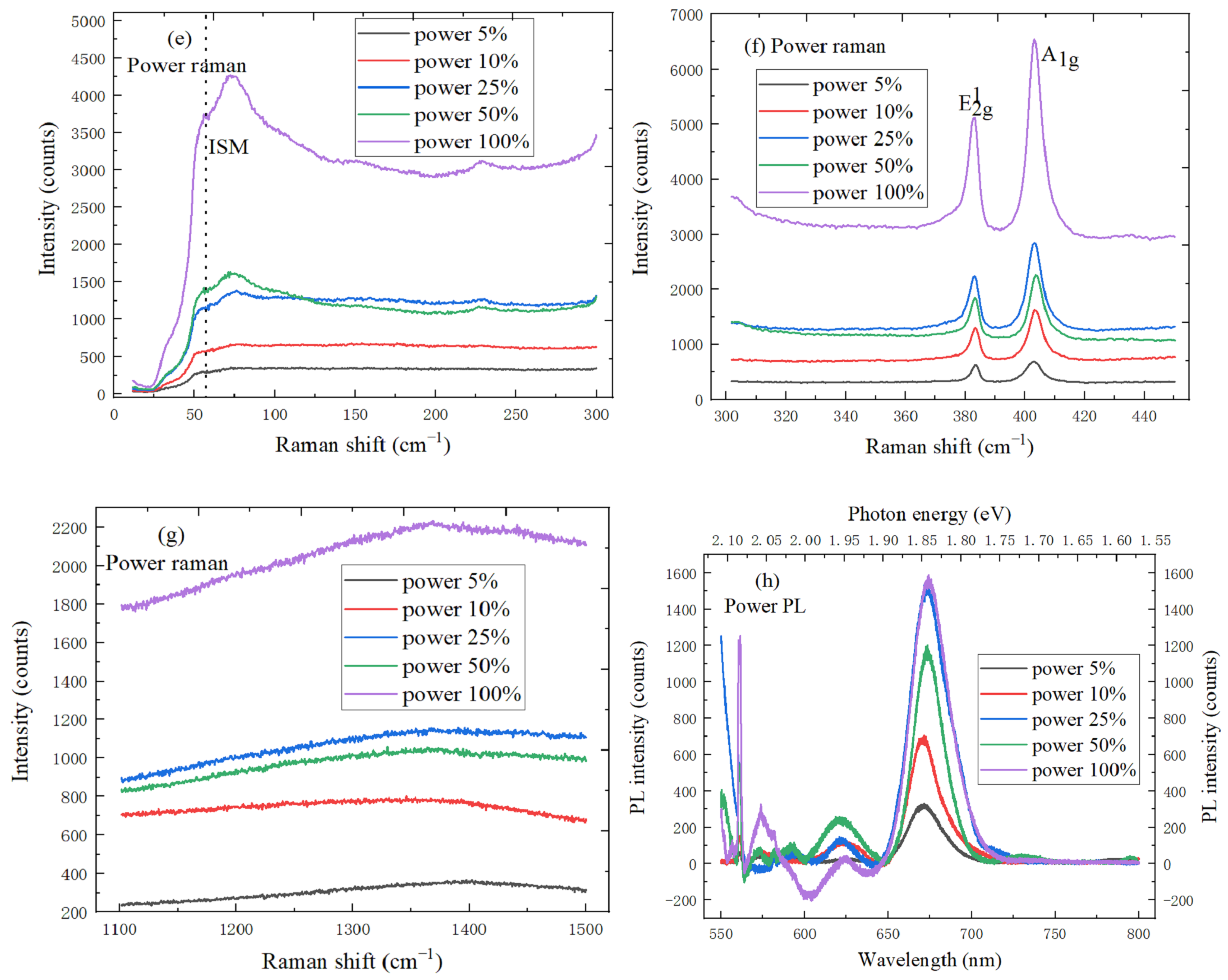
Figure 7f shows the power Raman spectrum of MoS2. The position shift of the characteristic peak varies with temperature, which is due to the temperature-dependent electron-phonon coupling and vdW interaction of MoS2/h-BN heterostructure. The E12g mode frequency of MoS2 becomes inversely proportional to the applied strain when the laser power increases, and the h-BN substrate appears with the blueshift, which is due to the reduced strain. The Alg mode frequency is also inversely related to the charge doping of MoS2, and Alg mode characteristic peak of MoS2 on h-BN is blue-shifted by 0.5 cm−1 compared with SiO2 substrate. In Figure 7g, IPM mode characteristic peak intensity of h-BN increases with the laser power increases, and the peak position shifts blue. Figure 7h shows the power PL spectrum of MoS2/h-BN heterostructure on SiO2/Si substrate. The characteristic peak intensity increases with the laser power increases, and the peak position shifts red when the temperature increases. Compared to the PL peak of monolayer MoS2/SiO2/Si substrate, the PL peak band gap of monolayer MoS2 grown on h-BN is closer to the mechanical peeling independent MoS2 sheet, peak position is blue-shifted, and the PL peak FWHM of MoS2/h-BN is smaller than that of MoS2/SiO2/Si substrate.
5. The Characterization of WS2/h-BN Heterostructure
5.1. The Optical Micrograph of WS2/h-BN Heterostructure
There are many dangling bonds at the edge of thin h-BN substrate, which can provide the nucleation sites during the growth of WS2. The unique crystallographic relationship indicates that there is the interaction between WS2 and h-BN. Due to the different electronegativity between B and N atoms, the charge density is polarized towards N atom. In addition to vdW forces, Coulomb interaction can also determine the orientation of WS2 on hBN.
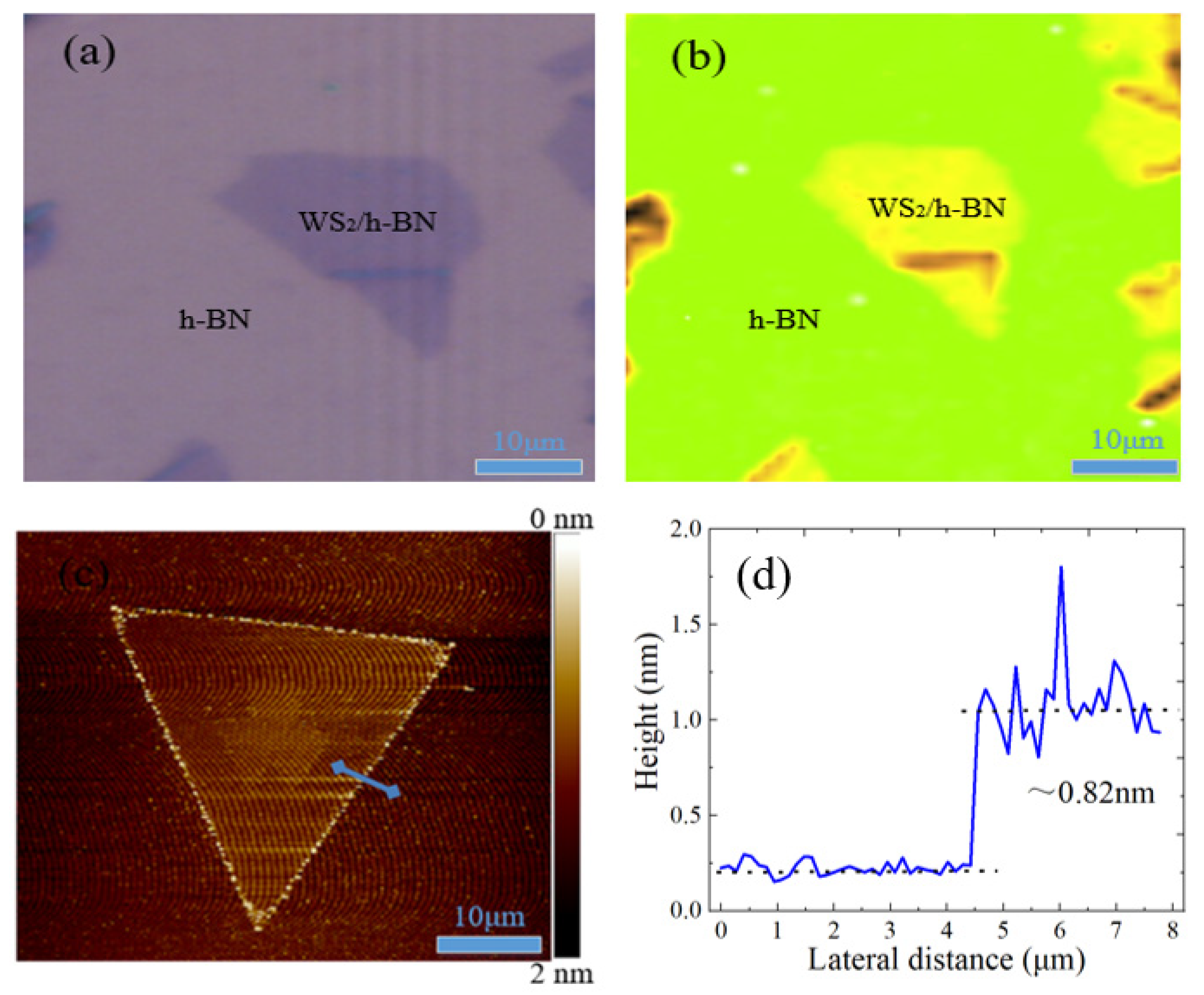
Due to the optical contrast, the surface morphology of WS2 nanosheets on h-BN/SiO2/Si substrate can be clearly observed by the optical microscope and AFM. Figure 8 shows the optical micrograph of WS2/h-BN heterostructure at different positions on SiO2/Si substrate, most region of the WS2 nanosheets have the good morphology and relatively uniform growth, which shows that the WS2 material has good film quality. Raman spectroscopy is an effective means to determine the strain distribution state of materials, the Raman spectrum mapping of WS2/h-BN heterojunction material was tested at the laser wavelength of 532 nm, and the uniform intensity distribution indicates that the homogeneity of heterojunction sample is very good, as shown in Figure 8b. The surface structure and properties of WS2/h-BN heterostructure sample were also characterized by AFM. In Figure 8c,d, the sample surface of WS2/h-BN heterojunction film is clean, there are lower roughnesses and defects, and the thickness of WS2 material is 0.82 nm, which indicates the presence of monolayer material.
5.2. The Spectral Characteristics of WS2
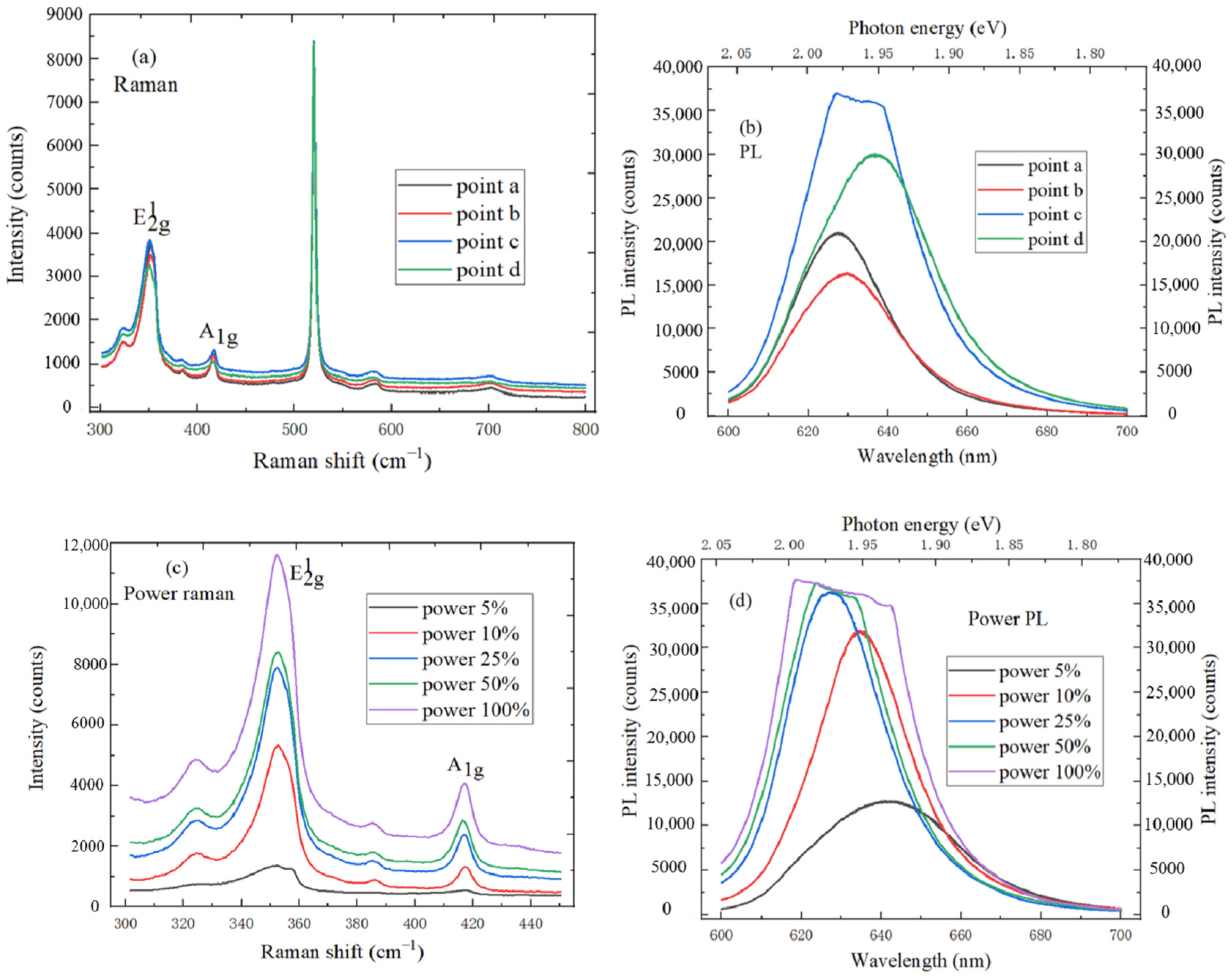
Figure 9a is the Raman spectrum of monolayer WS2 on SiO2/Si substrate under the four different test points, which is excited by 532 nm laser wavelength. The frequency difference between E12g and A1g modes characteristic peak decreases monotonously as the film thickness decreases, which can identify the layer number of WS2. The characteristic peak of E12g in-plane vibration mode and A1g out-of-plane vibration mode are, respectively, located at 353.5 cm−1 and 417.6 cm−1, the frequency difference is 64.1 cm−1, and the existence of monolayer WS2 material can be proved by observing Table 1. Figure 9b shows PL spectrum of WS2 at four different test points, and the strongest peak position of PL spectrum is 626 nm. It has a long exciton lifetime, coherence time, and the direct optical band gap of 1.98 eV at K and K′ symmetry points in the Brillouin zone, which can cause a significant PL phenomenon. In Figure 9c, the characteristic peak intensity of Raman spectrum accordingly increases as the laser power increases. As shown in Figure 9d, the PL intensity of WS2 increases as the laser power increases, and the strongest luminescence peak position shifts blue. The intensity of strongest PL spectrum no longer changes, and the FWHM increases when laser power exceeds 50%. This is because temperature increases as the laser power increases, and the dielectric shielding and exciton excitation effects of WS2 material can be weakened.
5.3. The Spectral Characteristics of WS2/h-BN Heterostructure
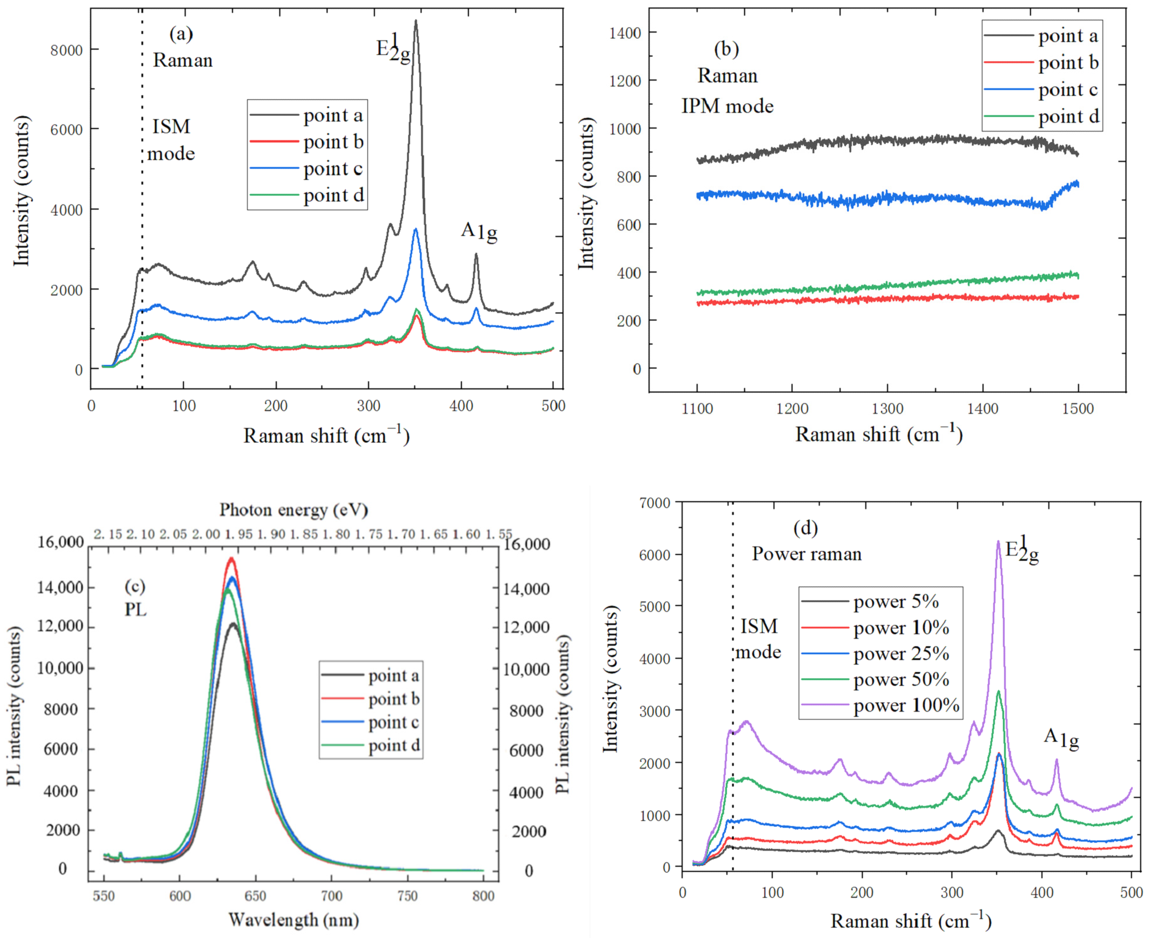
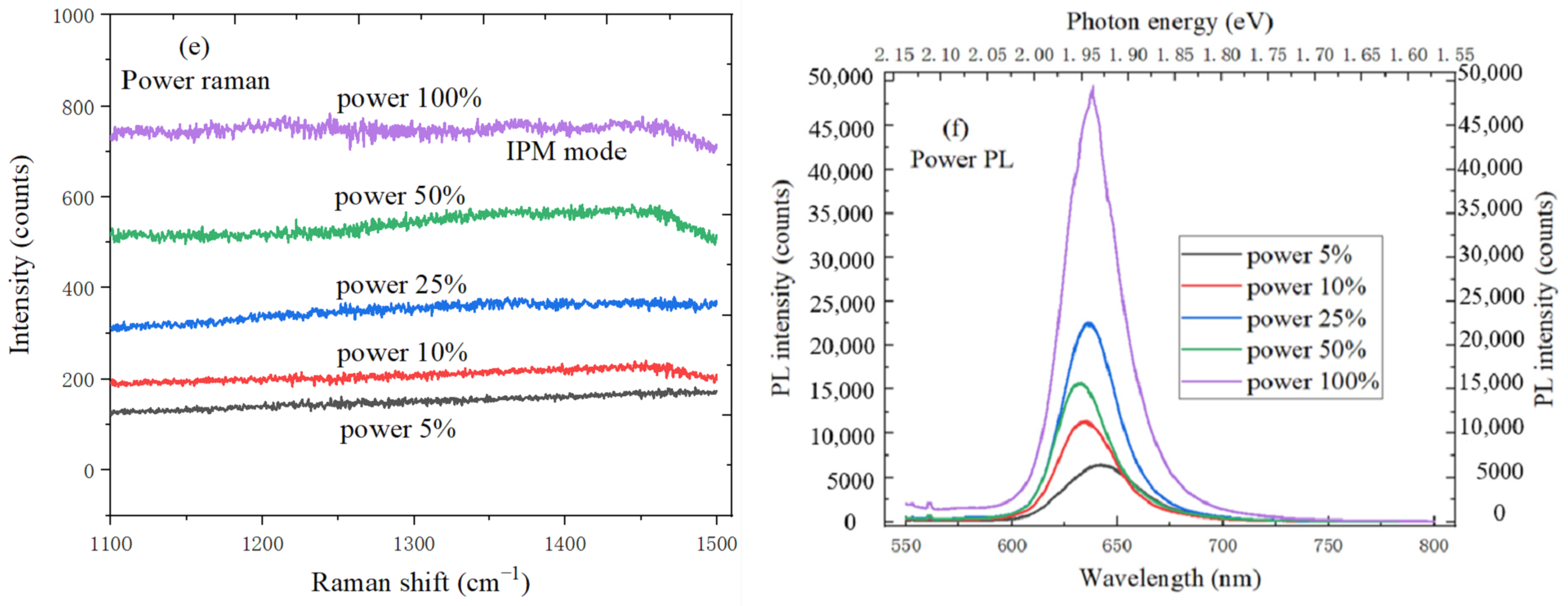
Figure 10a,b both show the Raman spectrum of WS2/h-BN heterostructure at four different test points, which is measured with an excitation wavelength of 532 nm. The E12g and A1g Raman activation mode characteristic peaks are, respectively, located at 356.3 and 416.6 cm−1, and the spacing is 60.3 cm−1, which corresponds to the reported peak spacing of monolayer WS2. Peak position movement is affected by the interaction between layers, and the E12g and A1g mode characteristic peaks are, respectively, red-shifted and blue-shifted when the layers number decreases. In addition, the IPM mode characteristic peak shape of WS2/h-BN is not obvious, the difference is attributed to the Van der Waals interaction between layers, and WS2 has the effect on the spectrum of h-BN. Figure 10c shows the PL spectrum of WS2/h-BN heterostructure at four different test points, the peak position of strongest PL spectrum is located at 1.96 eV, and the FWHM is only 56 meV, which is smaller than that of WS2. The FWHM of PL emission peak is related to the exciton lifetime and interface quality, and the WS2/h-BN heterostructure material has the higher crystallinity and cleaner interface. In addition, PL peak of WS2/h-BN is much brighter than that of WS2, so the hBN substrate plays the important role in the formation of high-quality thin WS2/h-BN heterostructure material. Figure 10d,e show the power Raman characteristic peaks of WS2/h-BN heterostructure, the intensities of ISM, IPM, E12g and A1g modes characteristic peaks accordingly increase as the laser power increases. The Raman vibration peak shape of E12g and A1g modes is sharp, which indicates that the prepared triangular WS2 nanosheets have good crystal quality. The Alg phonon wavenumber increases as the laser power increases, and the E12g mode wavenumber decreases. It can be considered as monolayer WS2 when Alg intensity is weak. This is because the coupling between electrons and phonons can strongly affect the Alg phonon of monolayer WS2, and the Alg peak intensity can be used to determine the thickness of the layer. Additionally, IPM mode characteristic peak intensity of h-BN also increases accordingly as the laser power increases. Figure 10f shows the strong PL spectrum of monolayer WS2, PL spectrum mainly comes from the charged exciton peak, peak position is 633 nm, and the corresponding photon energy is 1.96 eV, which is consistent with the direct band gap of monolayer WS2. Furthermore, the maximum FWHM is 74 meV, and the crystal quality of WS2 is high. As laser power increases, the peak intensity of strongest PL spectrum increases, and the peak position shifts blue.
6. Conclusions
In this paper, the general preparation methods of vdW heterostructure are provided. Monolayer MoS2 or WS2 can be directly grown on h-BN/SiO2/Si substrate by APCVD method, which can prepare TMDs/h-BN heterostructure. The test characterization of MoS2/h-BN and WS2/h-BN vdW heterostructure materials can be accomplished by the optical microscope, AFM, Raman and PL spectroscopy, and the TMDs/h-BN heterostructure has the tighter interlayer contact, clearer interface, smaller lattice strain and the lower doping level. The Raman characteristic peak signal intensity increases with the thickness of h-BN material increase. Raman and PL spectrum peak positions of MoS2/h-BN heterostructure show the blueshift compared with the spectrum of MoS2 or WS2 on SiO2/Si substrate. The reason is that there is the local strain and charged impurities, which can be caused by the h-BN substrate and the vdW heterostructure interaction. MoS2/h-BN heterostructure show the strong PL peak at 1.85 eV, which is closer to the mechanical peeling MoS2. The electron-phonon coupling and vdW interaction of MoS2/h-BN heterostructure can be enhanced by reducing the local strain and charged impurities. Furthermore, the strong and sharp PL emission peak of the WS2/h-BN heterostructure material is at 1.96 eV, and the FWHM of emission peak is only 56 meV, which is much smaller than the reported value. The quality of TMDs/hBN heterostructures is very high. In addition, IPM mode characteristic peak shape and peak position of WS2/h-BN is not obvious, and the difference is attributed to Van der Waals interaction. This research can prepare a variety of novel 2D heterostructures, and improve the basic interlayer coupling understanding of TMDs/h-BN heterostructure, which can provide guidance for the further application of vdW heterostructures in electronic and optoelectronic devices.
Author Contributions
Conceptualization and writing—original draft preparation, T.H. and Z.L.; methodology, S.W. and Y.C.; validation, T.H. and S.C.; writing—review and editing, H.L.; funding acquisition, H.L. All authors have read and agreed to the published version of the manuscript.
Funding
This research was funded by the National Natural Science Foundation of China (Grant No. U1866212, and 61904136), the Laboratory Open Fund of Beijing Smart-chip Microelectronics Technology Co., Ltd. (Grant No. SGITZXDDKJQT2002303), and the Fundamental Research Program of Shaanxi (Grant No. 2019JQ-656). This research was also supported by the national study fund and China Scholarship Council.
Conflicts of Interest
The authors declare no conflict of interest.
References
- Xu, W.; Kozawa, D.; Liu, Y.; Sheng, Y.; Wei, K.; Koman, V.B.; Wang, S.S.; Wang, X.C.; Jiang, T.; Strano, M.S.; et al. Determining the optimized interlayer separation distance in vertical stacked 2D WS2:hBN:MoS2 heterostructures for exciton energy transfer. Small 2018, 14, 1703727. [Google Scholar] [CrossRef] [PubMed]
- Hoshi, Y.; Kuroda, T.; Okada, M.; Moriya, R.; Masubuchi, S.; Watanabe, K.; Taniguchi, T.; Kitaura, R.; Machida, T. Suppression of exciton-exciton annihilation in tungsten disulfide monolayers encapsulated by hexagonal boron nitrides. Phys. Rev. B 2017, 95, 241403. [Google Scholar] [CrossRef] [Green Version]
- Ding, L.; Ukhtary, M.S.; Chubarov, M.; Choudhury, T.H.; Zhang, F.; Yang, R.; Zhang, A.; Fan, J.A.; Terrones, M.; Redwing, J.M.; et al. Understanding interlayer coupling in TMD-HBN heterostructure by Raman spectroscopy. IEEE Trans. Electron. Devices 2018, 65, 4059–4067. [Google Scholar] [CrossRef]
- Xu, W.; Kozawa, D.; Zhou, Y.; Wang, Y.; Sheng, Y.; Jiang, T.; Strano, M.S.; Warner, J.H. Controlling Photoluminescence Enhancement and Energy Transfer in WS2:hBN:WS2 Vertical Stacks by Precis Interlayer Distances. Small 2020, 16, 1905985. [Google Scholar] [CrossRef] [PubMed]
- Zollner, K.; Junior, P.E.F.; Fabian, J. Giant proximity exchange and valley splitting in transition metal dichalcogenide/h-BN/(Co, Ni) heterostructures. Phys. Rev. B 2020, 101, 085112. [Google Scholar] [CrossRef] [Green Version]
- Okada, M.; Kutana, A.; Kureishi, Y.; Kobayashi, Y.; Saito, Y.; Saito, T.; Watanabe, K.; Taniguchi, T.; Gupta, S.; Miyata, Y.; et al. Direct and indirect interlayer excitons in a van der Waals heterostructure of hBN/WS2/MoS2/hBN. ACS Nano 2018, 12, 2498–2505. [Google Scholar] [CrossRef]
- Zhang, F.; Wang, Y.; Erb, C.; Wang, K.; Moradifar, P.; Crespi, V.H.; Alem, N. Full orientation control of epitaxial MoS2 on hBN assisted by substrate defects. Phys. Rev. B 2019, 99, 155430. [Google Scholar] [CrossRef] [Green Version]
- Behura, S.; Nguyen, P.; Che, S.; Debbarma, R.; Berry, V. Large-area, transfer-free, oxide-assisted synthesis of hexagonal boron nitride films and their heterostructures with MoS2 and WS2. J. Am. Chem. Soc. 2015, 137, 13060–13065. [Google Scholar] [CrossRef]
- Athreya, N.; Leburton, J.P. Electronic Detection of Nucleotides in Multi-Layered MoS2-hBN Nanopore FET Devices. Biophys. J. 2020, 118, 157a. [Google Scholar] [CrossRef]
- Yosuke, U.; Alex, K.; Watanabe, K.; Taniguchi, T.; Kana, K.; Takahiko, E.; Yasumitsu, M.; Hisanori, S.; Ryo, K. Momentum-forbidden dark excitons in hBN-encapsulated monolayer MoS2. NPJ 2D Mater. Appl. 2019, 3, 1–6. [Google Scholar]
- Di Bartolomeo, A.; Genovese, L.; Giubileo, F.; Iemmo, L.; Luongo, G.; Foller, T.; Schleberger, M. Hysteresis in the transfer characteristics of MoS2 transistors. 2D Mater. 2017, 5, 015014. [Google Scholar] [CrossRef] [Green Version]
- Yang, H.; Gao, F.; Dai, M.; Jia, D.; Zhou, Y.; Hu, P. Recent advances in preparation, properties and device applications of two-dimensional h-BN and its vertical heterostructures. J. Semicond. 2017, 38, 031004. [Google Scholar] [CrossRef]
- Ahmed, T.; Bellare, P.; Debnath, R.; Roy, A.; Ravishankar, N.; Ghosh, A. Thermal History-Dependent Current Relaxation in hBN/MoS2 van der Waals Dimers. ACS Nano 2020, 14, 5909–5916. [Google Scholar] [CrossRef] [PubMed]
- Ahmed, T.; Roy, K.; Kakkar, S.; Pradhan, A.; Ghosh, A. Interplay of charge transfer and disorder in optoelectronic response in Graphene/hBN/MoS2 van der Waals heterostructures. 2D Mater. 2020, 7, 025043. [Google Scholar] [CrossRef]
- Datye, I.M.; Gabourie, A.J.; English, C.D.; Smithe, K.K.; McClellan, C.J.; Wang, N.C.; Pop, E. Reduction of hysteresis in MoS2 transistors using pulsed voltage measurements. 2D Mater. 2018, 6, 011004. [Google Scholar] [CrossRef]
- Lozovik, Y.E.; Kurbakov, I.L.; Volkov, P.A. Anisotropic superfluidity of two-dimensional excitons in a periodic potential. Phys. Rev. B 2017, 95, 245430. [Google Scholar] [CrossRef] [Green Version]
- Lim, H.; Yoon, S.I.; Kim, G.; Jang, A.R.; Shin, H.S. Stacking of two-dimensional materials in lateral and vertical directions. Chem. Mater. 2014, 26, 4891–4903. [Google Scholar] [CrossRef]
- Marchetto, D.; Restuccia, P.; Ballestrazzi, A.; Righi, M.C.; Rota, A.; Valeri, S. Surface passivation by graphene in the lubrication of iron: A comparison with bronze. Carbon 2017, 116, 375–380. [Google Scholar] [CrossRef] [Green Version]
- Wang, S.; Wang, X.; Warner, J.H. All chemical vapor deposition growth of MoS2: H-BN vertical van der Waals heterostructures. ACS Nano 2015, 9, 5246–5254. [Google Scholar] [CrossRef]
- Mitterreiter, E.; Schuler, B.; Cochrane, K.A.; Wurstbauer, U.; Weber-Bargioni, A.; Kastl, C.; Holleitner, A.W. Atomistic positioning of defects in helium ion treated single layer MoS2. Nano Lett. 2020, 20, 4437–4444. [Google Scholar] [CrossRef]
- Song, X.; Lu, L.; Wei, M.; Dai, Z.; Wang, S. Molecular dynamics simulations on the water flux in different two-dimension materials. Mol. Simul. 2020, 46, 689–698. [Google Scholar] [CrossRef]
- Li, Y.; Ye, F.; Xu, J.; Zhang, W.; Feng, P.X.L.; Zhang, X. Gate-Tuned Temperature in a Hexagonal Boron Nitride-Encapsulated 2-D Semiconductor Device. IEEE Trans. Electron. Devices 2018, 65, 4068–4072. [Google Scholar] [CrossRef]
- Okada, M.; Sawazaki, T.; Watanabe, K.; Taniguch, T.; Hibino, H.; Shinohara, H.; Kitaura, R. Direct chemical vapor deposition growth of WS2 atomic layers on hexagonal boron nitride. ACS Nano 2014, 8, 8273–8277. [Google Scholar] [CrossRef] [PubMed]
- Calman, E.V.; Fogler, M.M.; Butov, L.V.; Hu, S.; Mishchenko, A.; Geim, A.K. Indirect excitons in van der Waals heterostructures at room temperature. Nat. Commun. 2018, 9, 1–5. [Google Scholar] [CrossRef] [Green Version]
- Wells, C.C.; Melnikov, D.V.; Gracheva, M.E. Two Protein Dynamics through a Nanopore in an Electrically Biased Solid-State Membrane. Biophys. J. 2020, 118, 157a. [Google Scholar] [CrossRef]
- Rhodes, D.; Chae, S.H.; Ribeiro-Palau, R.; Hone, J. Disorder in van der Waals heterostructures of 2D materials. Nat. Mater. 2019, 18, 541. [Google Scholar] [CrossRef]
- Henriques, J.C.G.; Catarina, G.; Costa, A.T.; Fernández-Rossier, J.; Peres, N.M.R. Excitonic magneto-optical Kerr effect in two-dimensional transition metal dichalcogenides induced by spin proximity. Phys. Rev. B 2020, 101, 045408. [Google Scholar] [CrossRef] [Green Version]
- Iqbal, M.Z.; Siddique, S. Ultraviolet-light-driven enhanced hysteresis effect in graphene-tungsten disulfide heterostructures. Carbon 2017, 123, 168–173. [Google Scholar] [CrossRef]
- Ahmed, T.; Islam, S.; Tathagata, P.; Hariharan, N.; Elizabeth, S.; Ghosh, A. A generic method to control hysteresis and memory effect in Van der Waals hybrids. Mater. Res. Express 2020, 7, 014004. [Google Scholar] [CrossRef]
- Kamban, H.C.; Pedersen, T.G. Field-induced dissociation of two-dimensional excitons in transition metal dichalcogenides. Phys. Rev. B 2019, 100, 045307. [Google Scholar] [CrossRef] [Green Version]
- Saito, Y.; Kondo, T.; Ito, H.; Okada, M.; Shimizu, T.; Toshitaka, K.U.B.O.; Kitaura, R. Low frequency Raman study of interlayer couplings in WS2-MoS2 van der Waals heterostructures. Jpn. J. Appl. Phys. 2020, 59, 062004. [Google Scholar] [CrossRef]
- Chen, Y.; Quek, S.Y. Tunable bright interlayer excitons in few-layer black phosphorus based van der Waals heterostructures. 2D Mater. 2018, 5, 045031. [Google Scholar] [CrossRef]
- Esqueda, I.S.; Tian, H.; Yan, X.; Wang, H. Transport properties and device prospects of ultrathin black phosphorus on hexagonal boron nitride. IEEE Trans. Electron. Devices 2017, 64, 5163–5171. [Google Scholar] [CrossRef]
- Seo, S.G.; Joeng, J.; Kim, K.; Kim, K.; Jin, S.H. Bias Stress Instability in Multilayered MoS2 Field-Effect Transistors Under Pulse-Mode Operation. IEEE Trans. Electron. Devices 2020, 67, 1864–1872. [Google Scholar] [CrossRef]
Figure 1.
(a) Growth schematic diagram; (b) CVD temperature change curve of h-BN preparation.

Figure 2.
(a) CVD growth experiment schematic diagram; (b) Temperature change curve of TMDs/h-BN heterostructure.
Figure 2.
(a) CVD growth experiment schematic diagram; (b) Temperature change curve of TMDs/h-BN heterostructure.

Figure 3.
(a) Optical micrograph, (b) Raman spectrum mapping, (c) AFM and (d) height profile of MoS2/h-BN heterostructure on SiO2/Si substrate.
Figure 3.
(a) Optical micrograph, (b) Raman spectrum mapping, (c) AFM and (d) height profile of MoS2/h-BN heterostructure on SiO2/Si substrate.

Figure 4.
(a) ISM mode characteristic peaks of h-BN at different test points; (b) IPM mode characteristic peaks of h-BN at different test points; (c) ISM mode characteristic peaks of h-BN under the different laser power; (d) IPM mode characteristic peaks of h-BN under the different laser power.
Figure 4.
(a) ISM mode characteristic peaks of h-BN at different test points; (b) IPM mode characteristic peaks of h-BN at different test points; (c) ISM mode characteristic peaks of h-BN under the different laser power; (d) IPM mode characteristic peaks of h-BN under the different laser power.

Figure 5.
Spectral characteristics of h-BN with different layers (a) ISM mode characteristic peak spectrum; (b) IPM mode characteristic peak spectrum.
Figure 5.
Spectral characteristics of h-BN with different layers (a) ISM mode characteristic peak spectrum; (b) IPM mode characteristic peak spectrum.

Figure 6.
(a) Raman spectrum of MoS2 at three different test points; (b) PL spectrum of MoS2 at three different test points; (c) Raman spectrum of MoS2 under the different laser power; (d) PL spectrum of MoS2 under the different laser power; (e) Raman spectrum of MoS2 material with different layers; (f) Raman spectrum of MoS2 material with different layers.

Figure 7.
Spectral characteristics of MoS2/h-BN heterostructure. (a) ISM mode peak of h-BN at three different test points; (b) Raman peak of MoS2 at three different test points; (c) IPM mode peak of h-BN at three different test points; (d) PL spectrum of MoS2/h-BN heterostructure at three different test points; (e) ISM power mode peak of h-BN; (f) power Raman peak of MoS2; (g) IPM power mode peak of h-BN; (h) power PL spectrum of MoS2/h-BN heterostructure.


Figure 8.
(a) Optical micrograph, (b) Raman spectrum mapping, (c) AFM and (d) height profile of WS2/h-BN heterostructure on SiO2/Si substrate.
Figure 8.
(a) Optical micrograph, (b) Raman spectrum mapping, (c) AFM and (d) height profile of WS2/h-BN heterostructure on SiO2/Si substrate.

Figure 9.
(a) Raman spectrum of WS2 at four different test points; (b) PL spectrum of WS2 at four different test points; (c) Power Raman spectrum of WS2; (d) Power PL spectrum of WS2.
Figure 9.
(a) Raman spectrum of WS2 at four different test points; (b) PL spectrum of WS2 at four different test points; (c) Power Raman spectrum of WS2; (d) Power PL spectrum of WS2.

Figure 10.
Spectral characteristics of WS2/h-BN heterostructure (a) Raman characteristic peaks of h-BN ISM mode and MoS2 at four different teat points; (b) IPM mode characteristic peaks of h-BN at four different teat points; (c) PL spectrum of WS2/h-BN heterostructure at four different teat points; (d) power Raman characteristic peaks of h-BN ISM mode and MoS2; (e) IPM mode power characteristic peaks of h-BN; (f) power PL spectrum of WS2/h-BN heterostructure.


Table 1.
A1g peak and E12g peak positions of different WS2 layers.
| 1-Layers | 2-Layers | 3-Layers | Bulk | |
|---|---|---|---|---|
| E12g(Γ) (cm−1) | 352.1 | 350.9 | 349.8 | 348.7 |
| A1g(Γ) (cm−1) | 417.5 | 418.3 | 418.7 | 419.1 |
Publisher’s Note: MDPI stays neutral with regard to jurisdictional claims in published maps and institutional affiliations. |
© 2020 by the authors. Licensee MDPI, Basel, Switzerland. This article is an open access article distributed under the terms and conditions of the Creative Commons Attribution (CC BY) license (http://creativecommons.org/licenses/by/4.0/).
Share and Cite
MDPI and ACS Style
Han, T.; Liu, H.; Chen, S.; Chen, Y.; Wang, S.; Li, Z. Fabrication and Characterization of MoS2/h-BN and WS2/h-BN Heterostructures. Micromachines 2020, 11, 1114. https://doi.org/10.3390/mi11121114
AMA Style
Han T, Liu H, Chen S, Chen Y, Wang S, Li Z. Fabrication and Characterization of MoS2/h-BN and WS2/h-BN Heterostructures. Micromachines. 2020; 11(12):1114. https://doi.org/10.3390/mi11121114
Chicago/Turabian StyleHan, Tao, Hongxia Liu, Shupeng Chen, Yanning Chen, Shulong Wang, and Zhandong Li. 2020. "Fabrication and Characterization of MoS2/h-BN and WS2/h-BN Heterostructures" Micromachines 11, no. 12: 1114. https://doi.org/10.3390/mi11121114
Note that from the first issue of 2016, this journal uses article numbers instead of page numbers. See further details here.