Focused Electron Beam-Based 3D Nanoprinting for Scanning Probe Microscopy: A Review

 , , ,
, , ,  ,
, 
Abstract
:1. Introduction
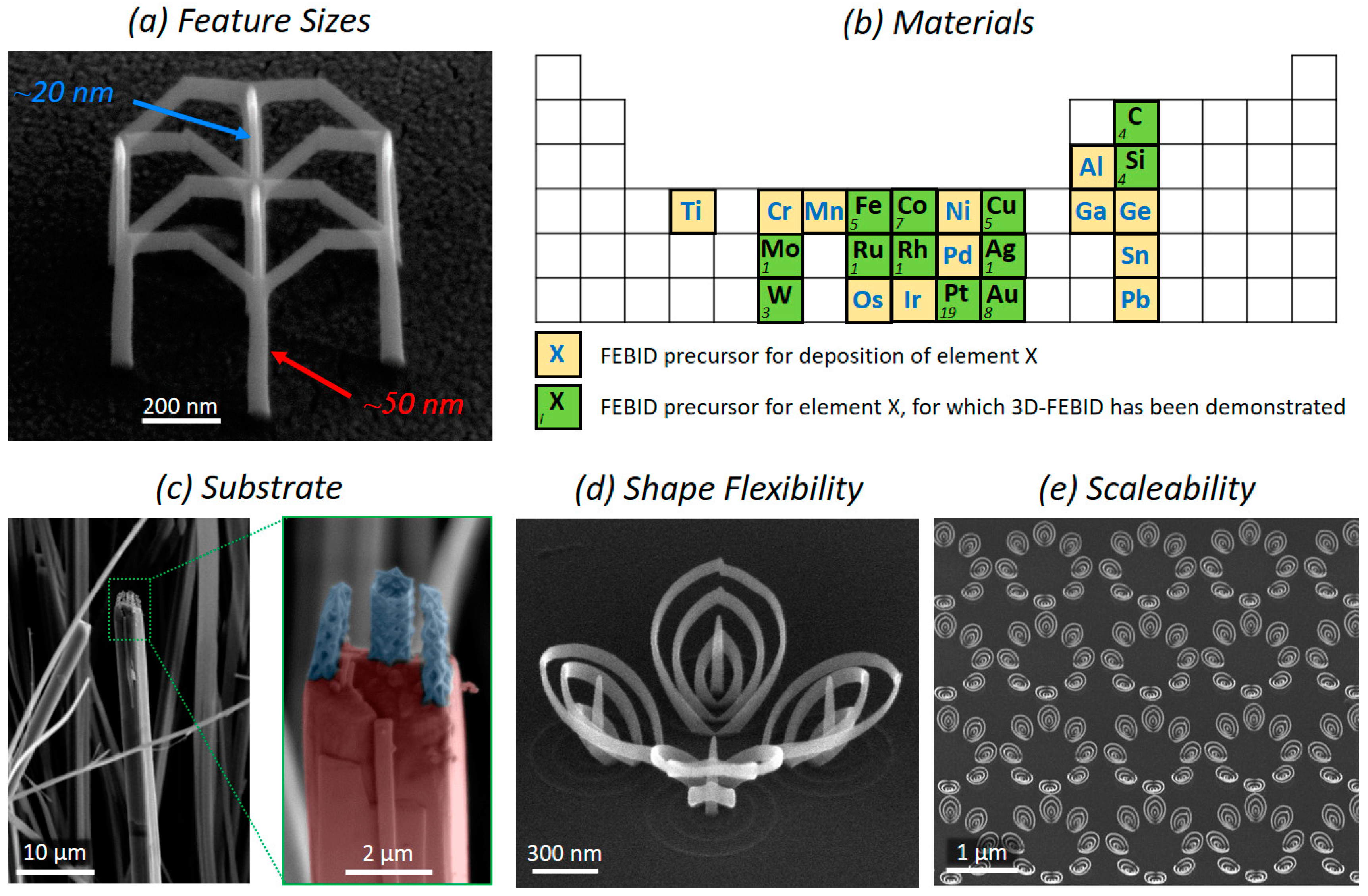
2. The Technology
2.1. Focused Electron Beam-Induced Deposition (FEBID)
2.2. 3D-FEBID
2.3. Demands on the Substrate
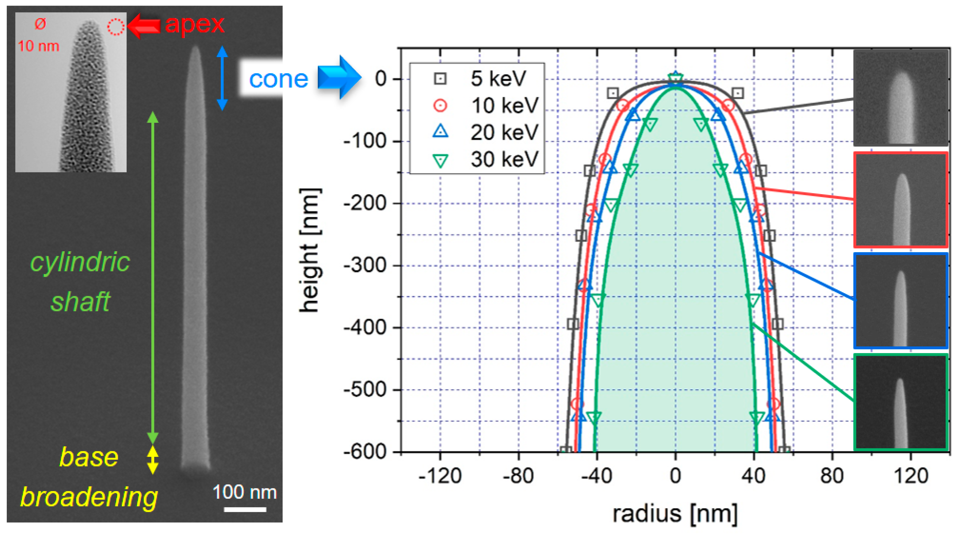
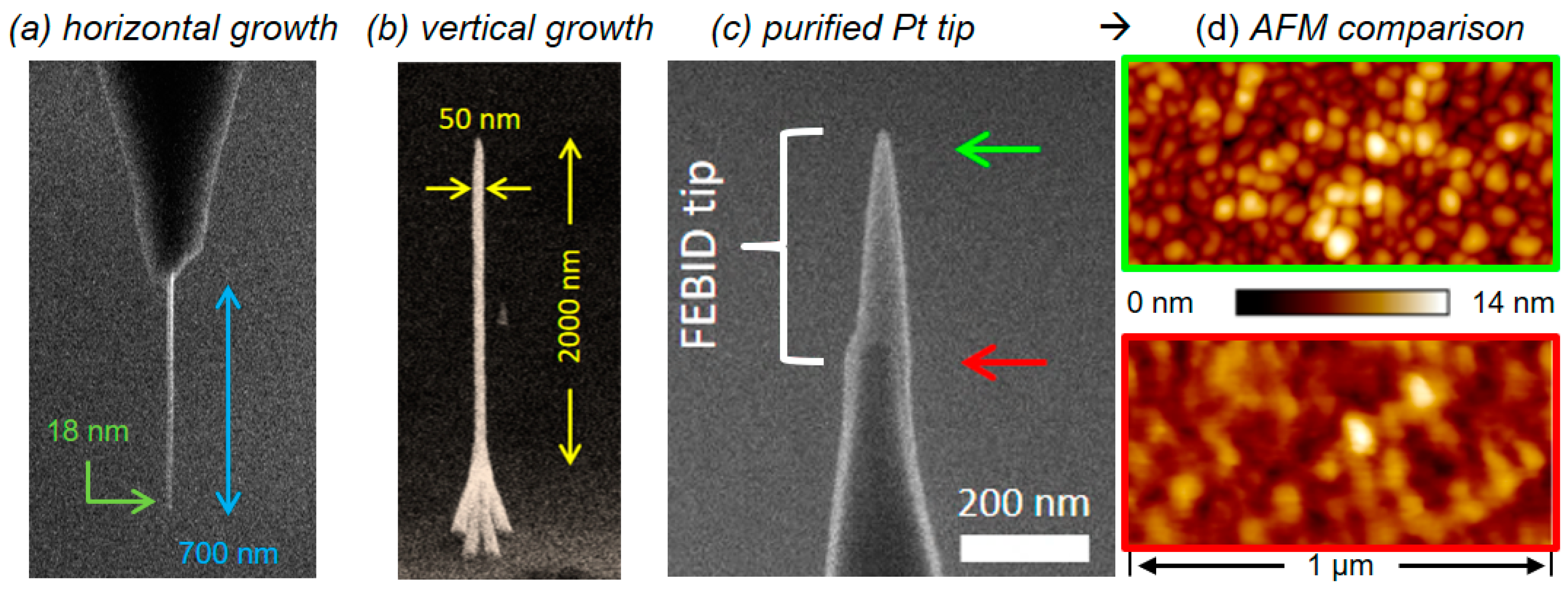
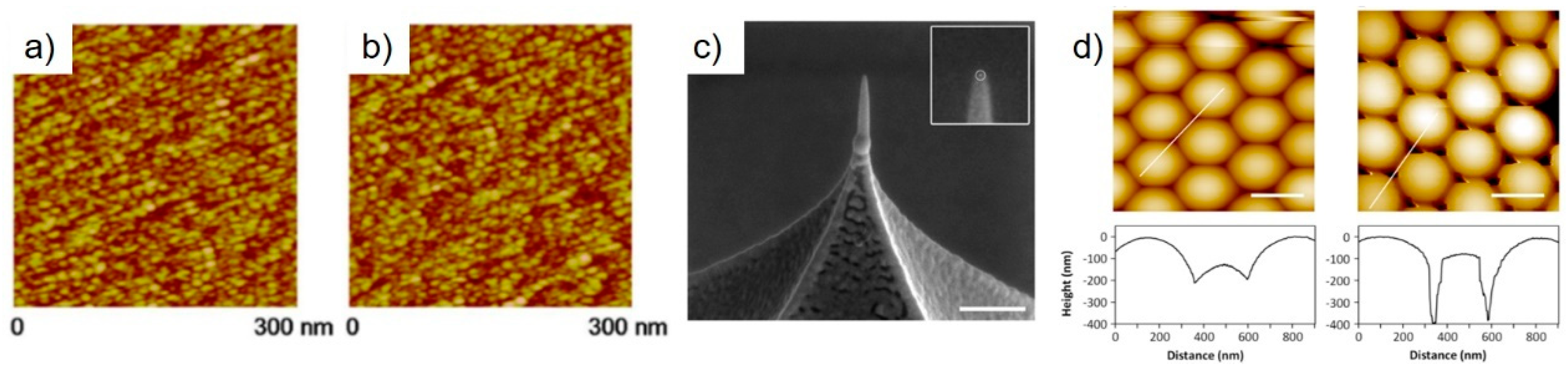
3. Feature Sizes
3.1. Intrinsic FEBID Feature Shapes
3.2. SPM Relevant Tailoring
3.3. Applications
3.4. Challenges
4. Materials and Functionalities
4.1. Applications
4.1.1. General AFM
4.1.2. Electric
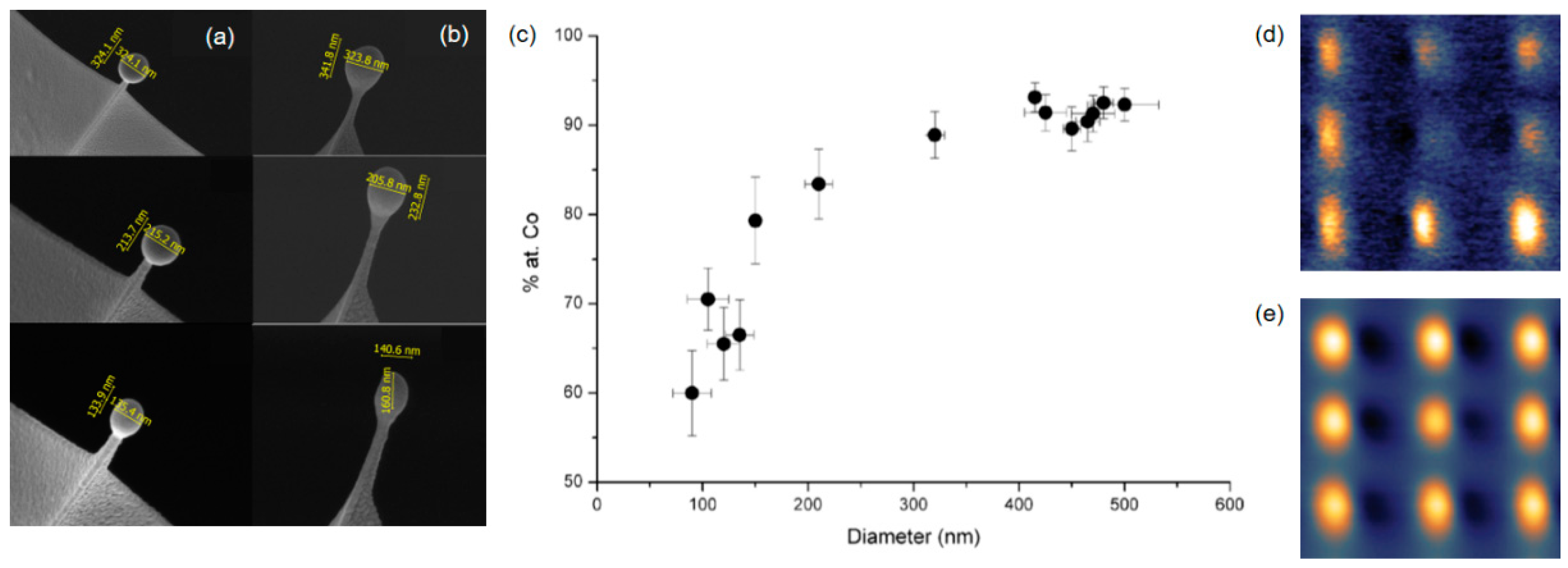
4.1.3. Magnetic
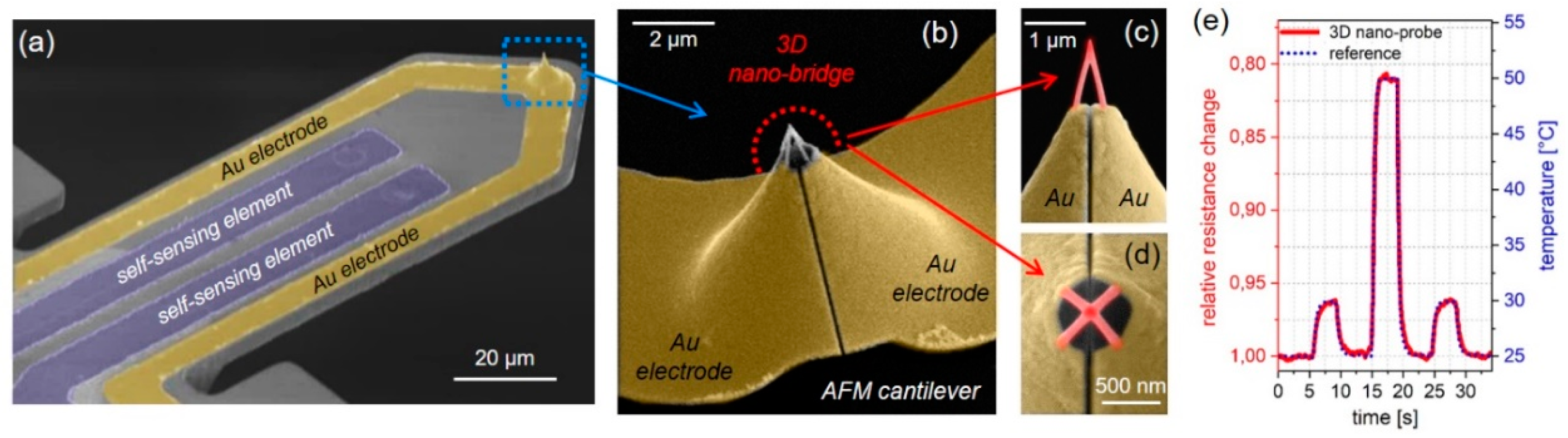
4.1.4. Thermal
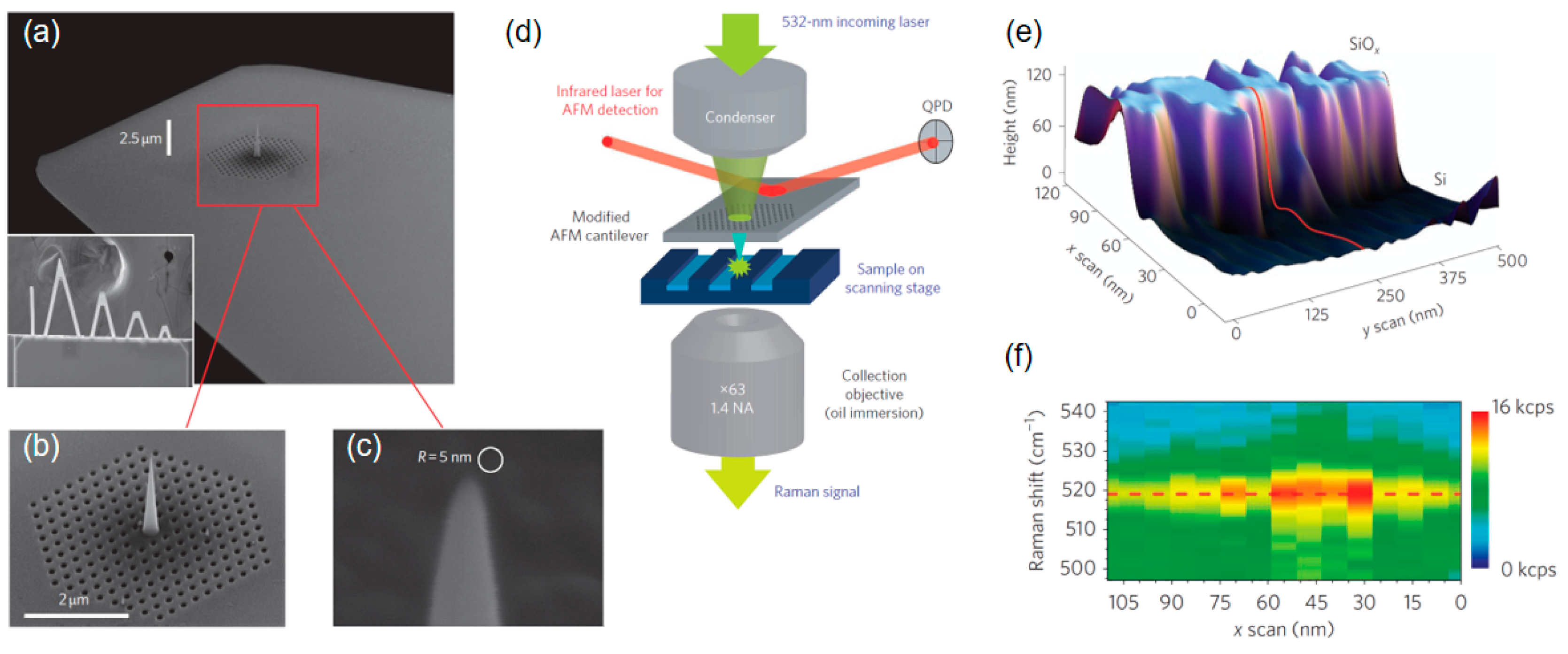
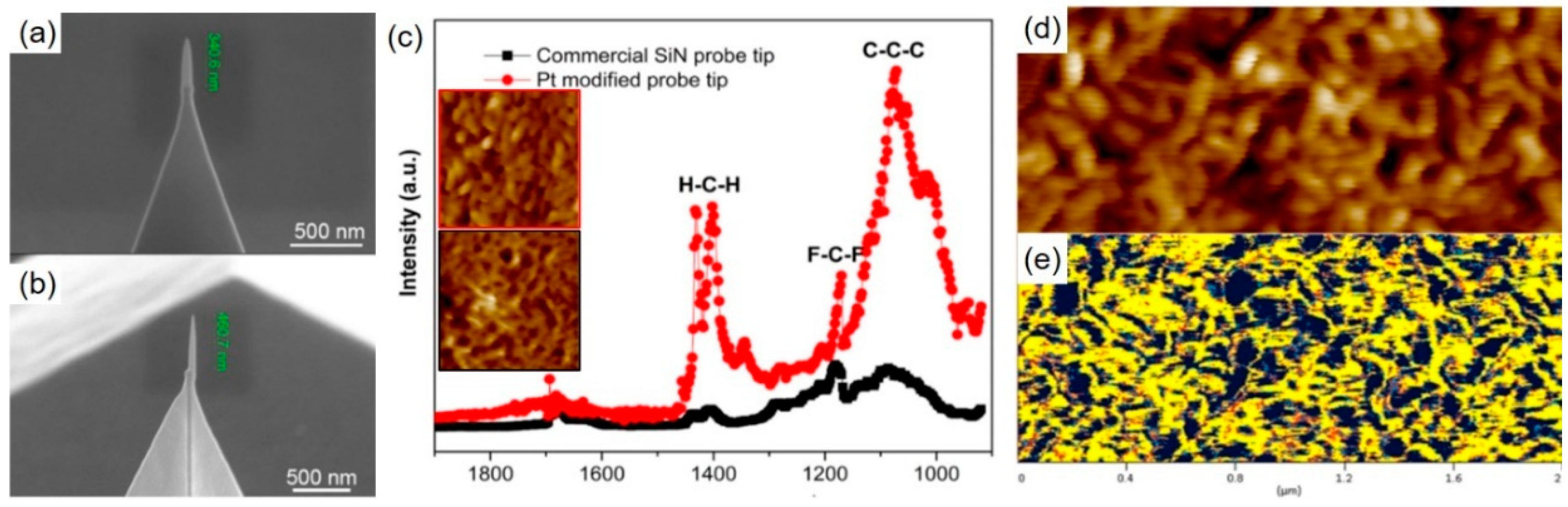
4.1.5. Optical
4.2. Challenges
5. Design Flexibility
5.1. Applications
5.2. Challenges
6. Scalability and Speed
7. Conclusions
Author Contributions
Funding
Acknowledgments
Conflicts of Interest
References
- Rodenbücher, C.; Wojtyniak, M.; Szot, K. Conductive AFM for Nanoscale Analysis of High-k Dielectric Metal Oxides. In Electrical Atomic Force Microscopy for Nanoelectronics; Springer: Cham, Switzerland, 2019; pp. 29–70. [Google Scholar]
- Gomes, S.; Assy, A.; Chapuis, P.-O. Scanning thermal microscopy: A review. Phys. Status Solidi Appl. Mater. Sci. 2015, 494, 477–494. [Google Scholar] [CrossRef]
- Grütter, P.; Mamin, H.J.; Rugar, D. Magnetic Force Microscopy (MFM). In Scanning Tunneling Microscopy II; Springer: Berlin, Germany, 1992; pp. 151–207. [Google Scholar]
- Melitz, W.; Shen, J.; Kummel, A.C.; Lee, S. Kelvin probe force microscopy and its application. Surf. Sci. Rep. 2011, 66, 1–27. [Google Scholar] [CrossRef]
- Cohen, S.R.; Bitler, A. Use of AFM in bio-related systems. Curr. Opin. Colloid Interface Sci. 2008, 13, 316–325. [Google Scholar] [CrossRef]
- Zhang, H.; Huang, J.; Wang, Y.; Liu, R.; Huai, X.; Jiang, J.; Anfuso, C. Atomic force microscopy for two-dimensional materials: A tutorial review. Opt. Commun. 2018, 406, 3–17. [Google Scholar] [CrossRef]
- Voigtländer, B. Scanning Probe Microscopy; NanoScience and Technology; Springer: Berlin/Heidelberg, Germany, 2015; ISBN 978-3-662-45239-4. [Google Scholar]
- Utke, I.; Moshkalev, S.; Russell, P.E. Nanofabrication Using Focused Ion and Electron Beams: Principles and Applications, 1st ed.; Utke, I., Moshkalev, S., Russell, P.E., Eds.; Oxford University Press: New York, NY, USA, 2012; ISBN 978-0199734214. [Google Scholar]
- Utke, I.; Hoffmann, P.; Melngailis, J. Gas-assisted focused electron beam and ion beam processing and fabrication. J. Vac. Sci. Technol. B Microelectron. Nanom. Struct. 2008, 26, 1197–1276. [Google Scholar] [CrossRef] [Green Version]
- Hirt, L.; Reiser, A.; Spolenak, R.; Zambelli, T. Additive Manufacturing of Metal Structures at the Micrometer Scale. Adv. Mater. 2017, 201604211, 1–30. [Google Scholar] [CrossRef] [PubMed]
- Giannuzzi, L.A.; Stevie, F.A. A review of focused ion beam milling techniques for TEM specimen preparation. Micron 1999, 30, 197–204. [Google Scholar] [CrossRef]
- Liang, T.; Frendberg, E.; Lieberman, B.; Stivers, A. Advanced photolithographic mask repair using electron beams. J. Vac. Sci. Technol. B Microelectron. Nanom. Struct. Process. Meas. Phenom. 2005, 23, 3101–3105. [Google Scholar] [CrossRef]
- Bret, T.; Hofmann, T.; Edinger, K. Industrial perspective on focused electron beam-induced processes. Appl. Phys. A 2014, 117, 1607–1614. [Google Scholar] [CrossRef]
- Noh, J.H.; Stanford, M.G.; Lewis, B.B.; Fowlkes, J.D.; Plank, H.; Rack, P.D. Nanoscale electron beam-induced deposition and purification of ruthenium for extreme ultraviolet lithography mask repair. Appl. Phys. A Mater. Sci. Process. 2014, 117, 1705–1713. [Google Scholar] [CrossRef]
- Mølhave, K.; Madsen, D.N.; Dohn, S.; Bøggild, P. Constructing, connecting and soldering nanostructures by environmental electron beam deposition. Nanotechnology 2004, 15, 1047–1053. [Google Scholar] [CrossRef]
- Schössler, C.; Urban, J.; Koops, H.W.P. Conductive supertips for scanning probe applications. J. Vac. Sci. Technol. B Microelectron. Nanom. Struct. 1997, 15, 1535–1538. [Google Scholar] [CrossRef]
- Wendel, M.; Irmer, B.; Cortes, J.; Kaiser, R.; Lorenz, H.; Kotthaus, J.P.; Lorke, A.; Williams, E. Nanolithography with an atomic force microscope. Superlattices Microstruct. 1996, 20, 349–356. [Google Scholar] [CrossRef]
- Schwalb, C.H.; Grimm, C.; Baranowski, M.; Sachser, R.; Porrati, F.; Reith, H.; Das, P.; Müller, J.; Völklein, F.; Kaya, A.; et al. A Tunable Strain Sensor Using Nanogranular Metals. Sensors 2010, 10, 9847–9856. [Google Scholar] [CrossRef] [PubMed]
- Gabureac, M.; Bernau, L.; Utke, I.; Boero, G. Granular Co-C nano-Hall sensors by focused-beam-induced deposition. Nanotechnology 2010, 21, 115503–115505. [Google Scholar] [CrossRef] [Green Version]
- Huth, M.; Kolb, F.; Plank, H. Dielectric sensing by charging energy modulation in a nano-granular metal. Appl. Phys. A 2014, 117, 1689–1696. [Google Scholar] [CrossRef] [Green Version]
- Arnold, G.; Winkler, R.; Stermitz, M.; Orthacker, A.; Noh, J.-H.; Fowlkes, J.D.; Kothleitner, G.; Huth, M.; Rack, P.D.; Plank, H. Tunable 3D Nanoresonators for Gas-Sensing Applications. Adv. Funct. Mater. 2018, 28, 1707387. [Google Scholar] [CrossRef]
- Huth, M.; Porrati, F.; Schwalb, C.; Winhold, M.; Sachser, R.; Dukic, M.; Adams, J.; Fantner, G. Focused electron beam induced deposition: A perspective. Beilstein J. Nanotechnol. 2012, 3, 597–619. [Google Scholar] [CrossRef] [Green Version]
- Huth, M.; Porrati, F.; Dobrovolskiy, O.V. Focused electron beam induced deposition meets materials science. Microelectron. Eng. 2018, 185, 9–28. [Google Scholar] [CrossRef] [Green Version]
- De Teresa, J.M.; Fernández-Pacheco, A.; Córdoba, R.; Serrano-Ramón, L.; Sangiao, M.; Ibarra, M.R.; Sangiao, S.; Ibarra, M.R. Review of magnetic nanostructures grown by focused electron beam induced deposition (FEBID). J. Phys. D. Appl. Phys. 2016, 49, 243003. [Google Scholar] [CrossRef]
- Kosters, D.; De Hoogh, A.; Zeijlemaker, H.; Acar, H.; Rotenberg, N.; Kuipers, L. Core-Shell Plasmonic Nanohelices. ACS Photonics 2017, 4, 1858–1863. [Google Scholar] [CrossRef] [PubMed] [Green Version]
- Béché, A.; Winkler, R.; Plank, H.; Hofer, F.; Verbeeck, J. Focused electron beam induced deposition as a tool to create electron vortices. Micron 2016, 80, 34–38. [Google Scholar] [CrossRef] [PubMed]
- Pakeltis, G.; Hu, Z.; Nixon, A.G.; Mutunga, E.; Anyanwu, C.P.; West, C.A.; Idrobo, J.C.; Plank, H.; Masiello, D.J.; Fowlkes, J.D.; et al. Focused Electron Beam Induced Deposition Synthesis of 3D Photonic and Magnetic Nanoresonators. ACS Appl. Nano Mater. 2019. [Google Scholar] [CrossRef]
- Brown, J.; Kocher, P.; Ramanujan, C.S.; Sharp, D.N.; Torimitsu, K.; Ryan, J.F. Electrically conducting, ultra-sharp, high aspect-ratio probes for AFM fabricated by electron-beam-induced deposition of platinum. Ultramicroscopy 2013, 133, 62–66. [Google Scholar] [CrossRef]
- Beard, J.D.; Gordeev, S.N. Fabrication and buckling dynamics of nanoneedle AFM probes. Nanotechnology 2011, 22, 175303. [Google Scholar] [CrossRef]
- Wendel, M.; Lorenz, H.; Kotthaus, J.P. Sharpened electron beam deposited tips for high resolution atomic force microscope lithography and imaging. Appl. Phys. Lett. 1995, 67, 3732–3734. [Google Scholar] [CrossRef]
- Zenhausern, F.; Adrian, M.; ten Heggeler-Bordier, B.; Ardizzoni, F.; Descouts, P. Enhanced imaging of biomolecules with electron beam deposited tips for scanning force microscopy. J. Appl. Phys. 1993, 73, 7232–7237. [Google Scholar] [CrossRef]
- Utke, I.; Hoffmann, P.; Berger, R.; Scandella, L. High-resolution magnetic Co supertips grown by a focused electron beam. Appl. Phys. Lett. 2002, 80, 4792–4794. [Google Scholar] [CrossRef]
- Winkler, R.; Lewis, B.B.; Fowlkes, J.D.; Rack, P.D.; Plank, H. High-Fidelity 3D-Nanoprinting via Focused Electron Beams: Growth Fundamentals. ACS Appl. Nano Mater. 2018, 1, 1014–1027. [Google Scholar] [CrossRef]
- Winkler, R.; Fowlkes, J.D.; Rack, P.D.; Plank, H. 3D nanoprinting via focused electron beams. J. Appl. Phys. 2019, 125, 210901. [Google Scholar] [CrossRef] [Green Version]
- Fernández-Pacheco, A.; Streubel, R.; Fruchart, O.; Fischer, P.; Cowburn, R.P.; Fern, A.; Streubel, R.; Fruchart, O.; Hertel, R.; Fischer, P. Three-dimensional nanomagnetism. Nat. Commun. 2017, 8, 15756. [Google Scholar] [CrossRef] [PubMed] [Green Version]
- Watson, J.H.L. Specimen Contamination in Electron Microscopes. J. Appl. Phys. 1948, 19, 110–111. [Google Scholar] [CrossRef]
- Van Dorp, W.F.; Hagen, C.W.; Crozier, P.A.; Kruit, P. Growth behavior near the ultimate resolution of nanometer-scale focused electron beam-induced deposition. Nanotechnology 2008, 19, 225305–225309. [Google Scholar] [CrossRef]
- Arnold, G.; Timilsina, R.; Fowlkes, J.D.; Orthacker, A.; Kothleitner, G.; Rack, P.D.; Plank, H. Fundamental resolution limits during electron induced direct write synthesis. ACS Appl. Mater. Interfaces 2014, 6, 7380–7387. [Google Scholar] [CrossRef] [PubMed]
- Kolb, F.; Schmoltner, K.; Huth, M.; Hohenau, A.; Krenn, J.; Klug, A.; List, E.J.W.; Plank, H. Variable tunneling barriers in FEBID based PtC metal-matrix nanocomposites as a transducing element for humidity sensing. Nanotechnology 2013, 24, 305501. [Google Scholar] [CrossRef] [PubMed]
- Winkler, R.; Szkudlarek, A.; Fowlkes, J.D.; Rack, P.D.; Utke, I.; Plank, H. Toward Ultraflat Surface Morphologies During Focused Electron Beam Induced Nanosynthesis: Disruption Origins and Compensation. ACS Appl. Mater. Interfaces 2015, 7, 3289–3297. [Google Scholar] [CrossRef]
- Yang, C.; Winkler, R.; Dukic, M.; Zhao, J.; Plank, H.; Fantner, G.E. Probing the Morphology and Evolving Dynamics of 3D Printed Nanostructures Using High-Speed Atomic Force Microscopy. ACS Appl. Mater. Interfaces 2017, 9, 24456–24461. [Google Scholar] [CrossRef]
- Gavagnin, M.; Wanzenboeck, H.D.; Wachter, S.; Shawrav, M.M.; Persson, A.; Gunnarsson, K.; Svedlindh, P.; Stöger-Pollach, M.; Bertagnolli, E. Free-standing magnetic nanopillars for 3D nanomagnet logic. ACS Appl. Mater. Interfaces 2014, 6, 20254–20260. [Google Scholar] [CrossRef]
- Van Dorp, W.F. A Database of FEBIP Literature. Available online: www.febip.org (accessed on 28 November 2019).
- Winkler, R.; Schmidt, F.-P.; Haselmann, U.; Fowlkes, J.D.; Lewis, B.B.; Kothleitner, G.; Rack, P.D.; Plank, H. Direct-Write 3D Nanoprinting of Plasmonic Structures. ACS Appl. Mater. Interfaces 2017, 9, 8233–8240. [Google Scholar] [CrossRef]
- Peinado, P.; Sangiao, S.; Teresa, J.M. De Focused Electron and Ion Beam Induced Deposition on Flexible and Transparent Polycarbonate Substrates. ACS Nano 2015, 9, 6139–6146. [Google Scholar] [CrossRef] [Green Version]
- Lewis, B.B.; Stanford, M.G.; Fowlkes, J.D.; Lester, K.; Plank, H.; Rack, P.D.; Huth, M.; Gölzhäuser, A. Electron-stimulated purification of platinum nanostructures grown via focused electron beam induced deposition. Beilstein J. Nanotechnol. 2015, 6, 1883–1885. [Google Scholar] [CrossRef] [PubMed] [Green Version]
- Friedli, V.; Utke, I. Optimized molecule supply from nozzle-based gas injection systems for focused electron- and ion-beam induced deposition and etching: Simulation and experiment. J. Phys. D. Appl. Phys. 2009, 42, 125305. [Google Scholar] [CrossRef]
- Winkler, R.; Fowlkes, J.; Szkudlarek, A.; Utke, I.; Rack, P.D.; Plank, H. The Nanoscale Implications of a Molecular Gas Beam during Electron Beam Induced Deposition. ACS Appl. Mater. Interfaces 2014, 6, 2987–2995. [Google Scholar] [CrossRef] [PubMed]
- Fowlkes, J.D.; Winkler, R.; Lewis, B.B.; Stanford, M.G.; Plank, H.; Rack, P.D. Simulation-Guided 3D Nanomanufacturing via Focused Electron Beam Induced Deposition. ACS Nano 2016, 10, 6163–6172. [Google Scholar] [CrossRef]
- Thorman, R.M.; Kumar, T.P.R.; Fairbrother, D.H.; Ingólfsson, O. The role of low-energy electrons in focused electron beam induced deposition: Four case studies of representative precursors. Beilstein J. Nanotechnol. 2015, 6, 1904–1926. [Google Scholar] [CrossRef] [Green Version]
- Plank, H.; Smith, D.A.; Haber, T.; Rack, P.D.; Hofer, F. Fundamental Proximity Effects in Focused Electron Beam Induced Deposition. ACS Nano 2012, 6, 286–294. [Google Scholar] [CrossRef]
- Smith, D.A.; Fowlkes, J.D.; Rack, P.D. Simulating the effects of surface diffusion on electron beam induced deposition via a three-dimensional Monte Carlo simulation. Nanotechnology 2008, 19, 415704–415711. [Google Scholar] [CrossRef]
- Smith, D.A.; Fowlkes, J.D.; Rack, P.D. Understanding the Kinetics and Nanoscale Morphology of Electron-Beam-Induced Deposition via a Three-Dimensional Monte Carlo Simulation: The Effects of the Precursor Molecule and the Deposited Material. Small J. 2008, 4, 1382–1389. [Google Scholar] [CrossRef]
- Smith, D.A.D.; Fowlkes, J.D.; Rack, P.D. A nanoscale three-dimensional Monte Carlo simulation of electron-beaminduced deposition with gas dynamics. Nanotechnology 2007, 18, 265308–265314. [Google Scholar] [CrossRef]
- Fowlkes, J.D.; Randolph, S.J.; Rack, P.D. Growth and simulation of high-aspect ratio nanopillars by primary and secondary electron-induced deposition. J. Vac. Sci. Technol. B 2005, 23, 2825–2832. [Google Scholar] [CrossRef] [Green Version]
- Choi, Y.R.; Rack, P.D.; Randolph, S.J.; Smith, D.A.; Joy, D.C. Pressure effect of growing with electron beam-induced deposition with tungsten hexafluoride and tetraethylorthosilicate precursor. Scanning 2007, 28, 311–318. [Google Scholar] [CrossRef] [PubMed] [Green Version]
- Frabboni, S.; Gazzadi, G.C.; Felisari, L.; Spessot, A. Fabrication by electron beam induced deposition and transmission electron microscopic characterization of sub-10-nm freestanding Pt nanowires. Appl. Phys. Lett. 2006, 88, 213113–213116. [Google Scholar] [CrossRef]
- Fujita, J.; Ishida, M.; Ichihashi, T.; Ochiai, Y.; Kaito, T.; Matsui, S. Carbon nanopillar laterally grown with electron beam-induced chemical vapor deposition. J. Vac. Sci. Technol. B 2003, 21, 2990–2993. [Google Scholar] [CrossRef]
- Ohnesorge, F.; Binnig, G. True Atomic Resolution by Atomic Force Microscopy Through Repulsive and Attractive Forces. Science 1993, 260, 1451–1456. [Google Scholar] [CrossRef]
- Hübner, B.; Koops, H.W.P.; Pagnia, H.; Sotnik, N.; Urban, J.; Weber, M. Tips for scanning tunneling microscopy produced by electron-beam-induced deposition. Ultramicroscopy 1992, 42, 1519–1525. [Google Scholar] [CrossRef]
- Schiffmann, K.I. Investigation of fabrication parameters for the electron-beam-induced deposition of contamination tips used in atomic force microscopy. Nanotechnology 1993, 4, 163–169. [Google Scholar] [CrossRef]
- Toth, M.; Lobo, C.; Friedli, V.; Szkudlarek, A.; Utke, I. Continuum models of focused electron beam induced processing. Beilstein J. Nanotechnol. 2015, 6, 1518–1540. [Google Scholar] [CrossRef]
- Rack, P.D.; Fowlkes, J.D.; Randolph, S.J. In situ probing of the growth and morphology in electron-beam-induced deposited nanostructures. Nanotechnology 2007, 18, 465602–465606. [Google Scholar] [CrossRef]
- Chen, I.-C.; Chen, L.-H.; Orme, C.; Quist, A.; Lal, R.; Jin, S. Fabrication of high-aspect-ratio carbon nanocone probes by electron beam induced deposition patterning. Nanotechnology 2006, 17, 4322–4326. [Google Scholar] [CrossRef]
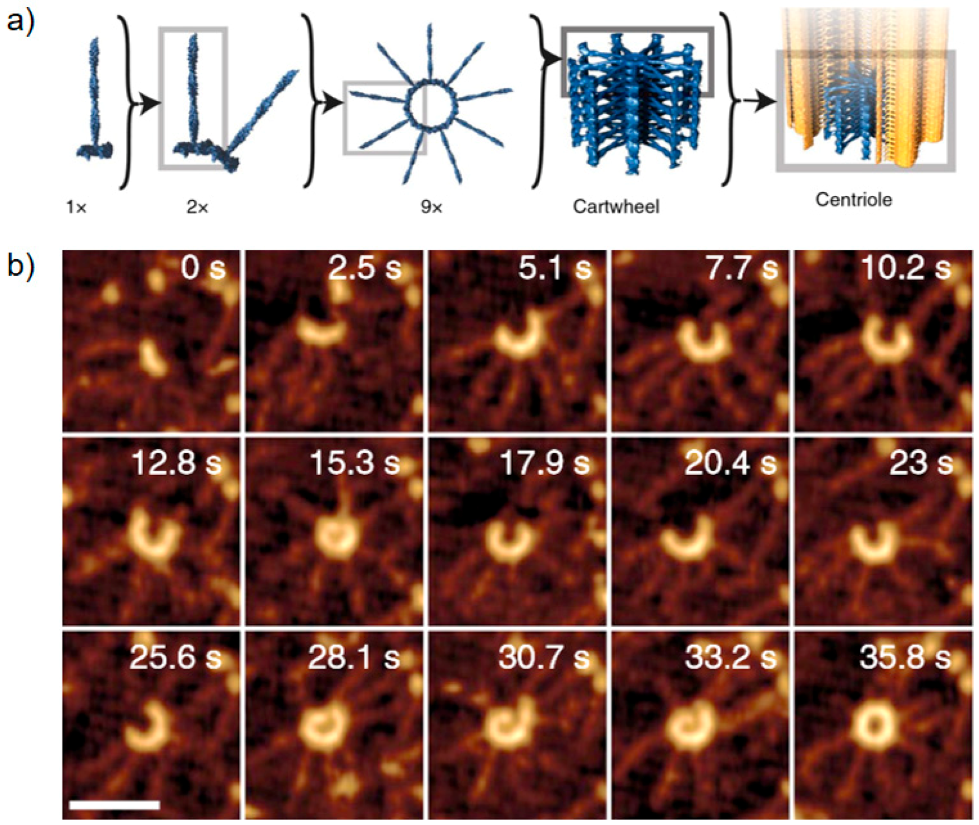
- Nievergelt, A.P.; Banterle, N.; Andany, S.H.; Gönczy, P.; Fantner, G.E. High-speed photothermal off-resonance atomic force microscopy reveals assembly routes of centriolar scaffold protein SAS-6. Nat. Nanotechnol. 2018, 13, 696–701. [Google Scholar] [CrossRef]
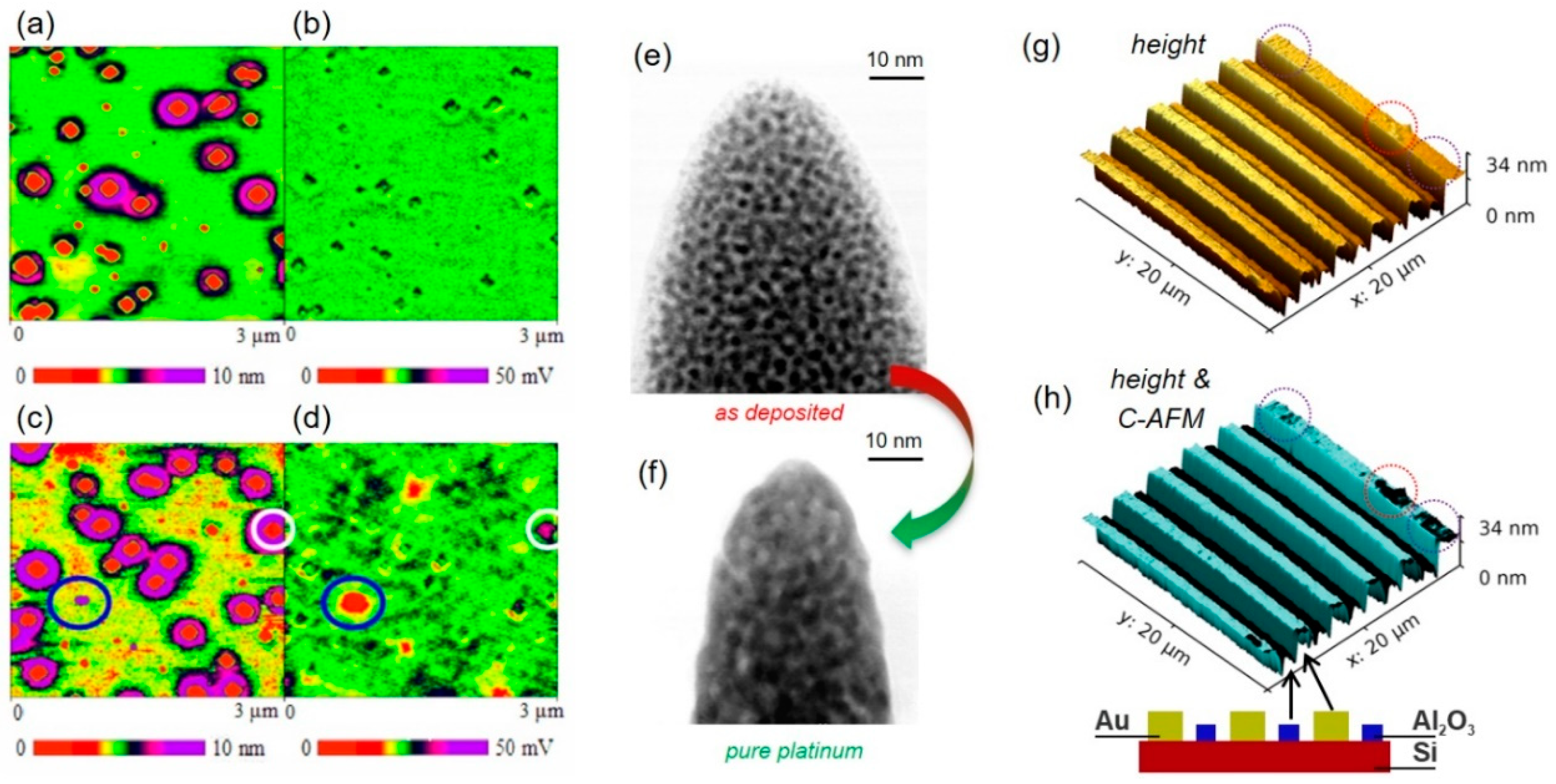
- Sattelkow, J.; Fröch, J.E.; Winkler, R.; Hummel, S.; Schwalb, C.; Plank, H. Three-Dimensional Nanothermistors for Thermal Probing. ACS Appl. Mater. Interfaces 2019, 11, 22655–22667. [Google Scholar] [CrossRef]
- Fowlkes, J.D.; Winkler, R.; Lewis, B.B.; Fernández-Pacheco, A.; Skoric, L.; Sanz-Hernández, D.; Stanford, M.G.; Mutunga, E.; Rack, P.D.; Plank, H. High-Fidelity 3D-Nanoprinting via Focused Electron Beams: Computer-Aided Design (3BID). ACS Appl. Nano Mater. 2018, 1, 1028–1041. [Google Scholar] [CrossRef]
- Porrati, F.; Pohlit, M.; Müller, J.; Barth, S.; Biegger, F.; Gspan, C.; Plank, H.; Huth, M. Direct writing of CoFe alloy nanostructures by focused electron beam induced deposition from a heteronuclear precursor. Nanotechnology 2015, 26, 475701. [Google Scholar] [CrossRef] [PubMed] [Green Version]
- Barry, J.D.; Ervin, M.; Molstad, J.; Wickenden, A.; Brintlinger, T.; Hoffman, P.; Meingailis, J. Electron beam induced deposition of low resistivity platinum from Pt(PF[sub 3])[sub 4]. J. Vac. Sci. Technol. B Microelectron. Nanom. Struct. 2006, 24, 3165. [Google Scholar] [CrossRef]
- Utke, I.; Hoffmann, P.; Dwir, B.; Leifer, K.; Kapon, E.; Doppelt, P. Focused electron beam induced deposition of gold. J. Vac. Sci. Technol. B 2000, 18, 3168–3171. [Google Scholar] [CrossRef]
- Klein, K.L.; Randolph, S.J.; Fowlkes, J.D.; Allard, L.F.; Meyer, H.M.; Simpson, M.L.; Rack, P.D. Single-crystal nanowires grown via electron-beam-induced deposition. Nanotechnology 2008, 19, 345705–345708. [Google Scholar] [CrossRef]
- Perentes, A.; Hoffmann, P. Oxygen assisted focused electron beam induced deposition of Si-containing materials: Growth dynamics. J. Vac. Sci. Technol. B 2007, 25, 2233–2238. [Google Scholar] [CrossRef]
- Höflich, K.; Jurczyk, J.M.; Madajska, K.; Götz, M.; Berger, L.; Guerra-Nuñez, C.; Haverkamp, C.; Szymanska, I.; Utke, I. Towards the third dimension in direct electron beam writing of silver. Beilstein J. Nanotechnol. 2018, 9, 842–849. [Google Scholar] [CrossRef] [Green Version]
- Winhold, M.; Schwalb, C.H.; Porrati, F.; Sachser, R.; Frangakis, A.S.; Kämpken, B.; Terfort, A.; Auner, N.; Huth, M. Binary Pt–Si Nanostructures Prepared by Focused Electron-Beam-Induced Deposition. ACS Nano 2011, 5, 9675–9681. [Google Scholar] [CrossRef]
- Botman, A.; Mulders, J.J.L.; Hagen, C.W. Creating pure nanostructures from electron-beam-induced deposition using purification techniques: A technology perspective. Nanotechnology 2009, 20, 372001. [Google Scholar] [CrossRef] [Green Version]
- Winkler, R.; Geier, B.; Plank, H. Spatial chemistry evolution during focused electron beam-induced deposition: Origins and workarounds. Appl. Phys. A 2014, 117, 1675–1688. [Google Scholar] [CrossRef]
- Plank, H.; Haber, T.; Gspan, C.; Kothleitner, G.; Hofer, F. Chemical tuning of PtC nanostructures fabricated via focused electron beam induced deposition. Nanotechnology 2013, 24, 175305. [Google Scholar] [CrossRef] [PubMed]
- Porrati, F.; Sachser, R.; Schwalb, C.H.; Frangakis, A.S.; Huth, M. Tuning the electrical conductivity of Pt-containing granular metals by postgrowth electron irradiation. J. Appl. Phys. 2011, 109, 063715. [Google Scholar] [CrossRef] [Green Version]
- Trummer, C.; Winkler, R.; Plank, H.; Kothleitner, G.; Haberfehlner, G. Analyzing the Nanogranularity of Focused-Electron-Beam-Induced-Deposited Materials by Electron Tomography. ACS Appl. Nano Mater. 2019, 2, 5356–5359. [Google Scholar] [CrossRef]
- Plank, H.; Kothleitner, G.; Hofer, F.; Michelitsch, S.G.; Gspan, C.; Hohenau, A.; Krenn, J. Optimization of postgrowth electron-beam curing for focused electron-beam-induced Pt deposits. J. Vac. Sci. Technol. B 2011, 29, 51801–51807. [Google Scholar] [CrossRef]
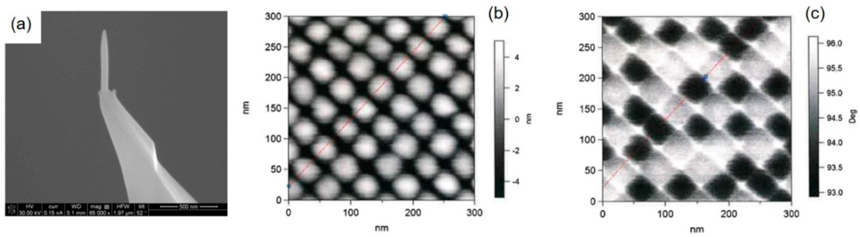
- Lewis, B.B.; Mound, B.A.; Srijanto, B.; Fowlkes, J.D.; Pharr, G.M.; Rack, P.D. Growth and nanomechanical characterization of nanoscale 3D architectures grown via focused electron beam induced deposition. Nanoscale 2017, 9, 16349–16356. [Google Scholar] [CrossRef]
- Huth, M. Granular metals: From electronic correlations to strain-sensing applications. J. Appl. Phys. 2010, 107, 113709. [Google Scholar] [CrossRef]
- Shawrav, M.M.; Taus, P.; Wanzenboeck, H.D.; Schinnerl, M.; Stöger-Pollach, M.; Schwarz, S.; Steiger-Thirsfeld, A.; Bertagnolli, E. Highly conductive and pure gold nanostructures grown by electron beam induced deposition. Sci. Rep. 2016, 6, 34003. [Google Scholar] [CrossRef] [Green Version]
- Lewis, B.B.; Winkler, R.; Sang, X.; Pudasaini, P.R.; Stanford, M.G.; Plank, H.; Unocic, R.R.; Fowlkes, J.D.; Rack, P.D. 3D Nanoprinting via laser-assisted electron beam induced deposition: Growth kinetics, enhanced purity, and electrical resistivity. Beilstein J. Nanotechnol. 2017, 8, 801–812. [Google Scholar] [CrossRef] [Green Version]
- Mølhave, K.; Madsen, D.N.; Rasmussen, A.M.; Carlsson, A.; Appel, C.C.; Brorson, M.; Jacobsen, C.J.H.; Bøggild, P. Solid Gold Nanostructures Fabricated by Electron Beam Deposition. Nano Lett. 2003, 3, 1499–1503. [Google Scholar] [CrossRef]
- Folch, A.; Tejada, J.; Peters, C.H.; Wrighton, M.S. Electron beam deposition of gold nanostructures in a reactive environment. Appl. Phys. Lett. 1995, 66, 2080–2082. [Google Scholar] [CrossRef] [Green Version]
- Langford, R.M.; Ozkaya, D.; Sheridan, J.; Chater, R. Effects of Water Vapour on Electron and Ion Beam Deposited Platinum. Microsc. Microanal. 2004, 10, 1122–1123. [Google Scholar] [CrossRef]
- Perentes, A.; Hoffmann, P. Focused Electron Beam Induced Deposition of Si-Based Materials From SiOxCy to Stoichiometric SiO2: Chemical Compositions, Chemical-Etch Rates, and Deep Ultraviolet Optical Transmissions. Chem. Vap. Depos. 2007, 13, 176–184. [Google Scholar] [CrossRef]
- Spencer, J.A.; Barclay, M.; Gallagher, M.J.; Winkler, R.; Unlu, I.; Wu, Y.-C.; Plank, H.; McElwee-White, L.; Fairbrother, D.H. Comparing postdeposition reactions of electrons and radicals with Pt nanostructures created by focused electron beam induced deposition. Beilstein J. Nanotechnol. 2017, 8, 2410–2424. [Google Scholar] [CrossRef] [PubMed] [Green Version]
- Geier, B.; Gspan, C.; Winkler, R.; Schmied, R.; Fowlkes, J.D.; Fitzek, H.; Rauch, S.; Rattenberger, J.; Rack, P.D.; Plank, H. Rapid and Highly Compact Purification for Focused Electron Beam Induced Deposits: A Low Temperature Approach Using Electron Stimulated H 2 O Reactions. J. Phys. Chem. C 2014, 118, 14009–14016. [Google Scholar] [CrossRef]
- Mehendale, S.; Mulders, J.J.L.; Trompenaars, P.H.F. A new sequential EBID process for the creation of pure Pt structures from MeCpPtMe3. Nanotechnology 2013, 24, 145303. [Google Scholar] [CrossRef] [PubMed]
- Utke, I.; Michler, J.; Plank, H. Mechanical properties of 3D nanostructures obtained by gas assisted focused electron beam and ion beam induced deposition: A Review. Micromachines 2020, in press. [Google Scholar]
- Nanotools. Available online: www.nanotools.com (accessed on 28 November 2019).
- Chen, P.L.; Su, J.; Shiao, M.H.; Chang, M.N.; Lee, C.H.; Liu, C.W. Scanning electron beam induced deposition for conductive tip modification. In Proceedings of the 2012 7th IEEE International Conference on Nano/Micro Engineered and Molecular Systems (NEMS), Kyoto, Japan, 5–8 March 2012; pp. 553–556. [Google Scholar]
- GETec Microscopy. Available online: www.getec-afm.com (accessed on 28 November 2019).
- Noh, J.H.; Nikiforov, M.; Kalinin, S.V.; Vertegel, A.A.; Rack, P.D. Nanofabrication of insulated scanning probes for electromechanical imaging in liquid solutions. Nanotechnology 2010, 21, 365302. [Google Scholar] [CrossRef]
- Roberts, N.A.; Noh, J.H.; Lassiter, M.G.; Guo, S.; Kalinin, S.V.; Rack, P.D. Synthesis and electroplating of high resolution insulated carbon nanotube scanning probes for imaging in liquid solutions. Nanotechnology 2012, 23, 145301. [Google Scholar] [CrossRef]
- Lau, Y.M.; Chee, P.C.; Thong, T.L.; Ng, V. Properties and applications of cobalt-based material produced by electron-beam-induced deposition. J. Vac. Sci. Technol. A 2002, 20, 1295–1302. [Google Scholar] [CrossRef] [Green Version]
- Utke, I.; Cicoira, F.; Jaenchen, G.; Hoffmann, P.; Scandella, L.; Dwir, B.; Kapon, E.; Laub, D.; Buffat, P.; Xanthopoulos, N.; et al. Focused Electron Beam Induced Deposition of High Resolution Magnetic Scanning Probe Tips. MRS Online Proc. Libr. Arch. 2001, 706, Z9.24.1. [Google Scholar] [CrossRef]
- Fernández-Pacheco, A.; De Teresa, J.M.; Córdoba, R.; Ibarra, M.R. Magnetotransport properties of high-quality cobalt nanowires grown by focused-electron-beam-induced deposition. J. Phys. D Appl. Phys. 2009, 42, 055005. [Google Scholar] [CrossRef] [Green Version]
- Córdoba, R.; Sesé, J.; De Teresa, J.M.; Ibarra, M.R. High-purity cobalt nanostructures grown by focused-electron-beam-induced deposition at low current. Microelectron. Eng. 2010, 87, 1550–1553. [Google Scholar] [CrossRef]
- Bernau, L.; Gabureac, M.; Erni, R.; Utke, I. Tunable Nanosynthesis of Composite Materials by Electron-Impact Reaction. Angew. Chem. Int. Ed. 2010, 49, 8880–8884. [Google Scholar] [CrossRef] [PubMed] [Green Version]
- Serrano-Ramón, L.; Córdoba, R.; Rodríguez, L.A.; Magén, C.; Snoeck, E.; Gatel, C.; Serrano, I.; Ibarra, M.R.; De Teresa, J.M. Ultrasmall functional ferromagnetic nanostructures grown by focused electron-beam-induced deposition. ACS Nano 2011, 5, 7781–7787. [Google Scholar] [CrossRef] [Green Version]
- Pablo-Navarro, J.; Winkler, R.; Haberfehlner, G.; Magén, C.; Plank, H.; De Teresa, J.M. In situ real-time annealing of ultrathin vertical Fe nanowires grown by focused electron beam induced deposition. Acta Mater. 2019, 174, 379–386. [Google Scholar] [CrossRef]
- Takeguchi, M.; Shimojo, M.; Furuya, K. Fabrication of magnetic nanostructures using electron beam induced chemical vapour deposition. Nanotechnology 2005, 16, 1321–1325. [Google Scholar] [CrossRef]
- Zhang, W.; Shimojo, M.; Takeguchi, M.; Che, R.-C.; Furuya, K. Generation Mechanism and in situ Growth Behavior of α-Iron Nanocrystals by Electron Beam Induced Deposition. Adv. Eng. Mater. 2006, 8, 711–714. [Google Scholar] [CrossRef]
- Rodríguez, L.A.; Deen, L.; Córdoba, R.; Magén, C.; Snoeck, E.; Koopmans, B.; De Teresa, J.M. Influence of the shape and surface oxidation in the magnetization reversal of thin iron nanowires grown by focused electron beam induced deposition. Beilstein J. Nanotechnol. 2015, 6, 1319–1331. [Google Scholar] [CrossRef] [Green Version]
- Venturi, F.; Gazzadi, G.C.; Tavabi, A.H.; Rota, A.; Dunin-Borkowski, R.E.; Frabboni, S. Magnetic characterization of cobalt nanowires and square nanorings fabricated by focused electron beam induced deposition. Beilstein J. Nanotechnol. 2018, 9, 1040–1049. [Google Scholar] [CrossRef] [Green Version]
- Wolf, D.; Rodriguez, L.A.; Béché, A.; Javon, E.; Serrano, L.; Magen, C.; Gatel, C.; Lubk, A.; Lichte, H.; Bals, S.; et al. 3D Magnetic Induction Maps of Nanoscale Materials Revealed by Electron Holographic Tomography. Chem. Mater. 2015, 27, 6771–6778. [Google Scholar] [CrossRef] [PubMed]
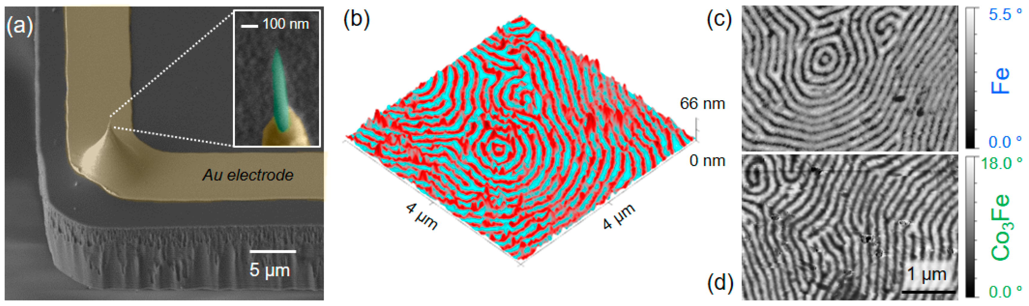
- Stiller, M.; Barzola-Quiquia, J.; Esquinazi, P.D.; Sangiao, S.; De Teresa, J.M.; Meijer, J.; Abel, B. Functionalized Akiyama tips for magnetic force microscopy measurements. Meas. Sci. Technol. 2017, 28, 125401. [Google Scholar] [CrossRef] [Green Version]
- Belova, L.M.; Hellwig, O.; Dobisz, E.; Dan Dahlberg, E. Rapid preparation of electron beam induced deposition Co magnetic force microscopy tips with 10 nm spatial resolution. Rev. Sci. Instrum. 2012, 83, 093711. [Google Scholar] [CrossRef] [PubMed]
- Pablo-Navarro, J.; Magén, C.; de Teresa, J.M. Three-dimensional core–shell ferromagnetic nanowires grown by focused electron beam induced deposition. Nanotechnology 2016, 27, 285302. [Google Scholar] [CrossRef]
- Keller, L.; Al Mamoori, M.K.I.; Pieper, J.; Gspan, C.; Stockem, I.; Schröder, C.; Barth, S.; Winkler, R.; Plank, H.; Pohlit, M.; et al. Direct-write of free-form building blocks for artificial magnetic 3D lattices. Sci. Rep. 2018, 8, 6160. [Google Scholar] [CrossRef] [Green Version]
- Al Mamoori, M.; Keller, L.; Pieper, J.; Barth, S.; Winkler, R.; Plank, H.; Müller, J.; Huth, M. Magnetic Characterization of Direct-Write Free-Form Building Blocks for Artificial Magnetic 3D Lattices. Materials. 2018, 11, 289. [Google Scholar] [CrossRef] [Green Version]
- Ragesh Kumar, T.P.; Unlu, I.; Barth, S.; Ingólfsson, O.; Fairbrother, D.H. Electron Induced Surface Reactions of HFeCo 3 (CO) 12, a Bimetallic Precursor for Focused Electron Beam Induced Deposition (FEBID). J. Phys. Chem. C 2018, 122, 2648–2660. [Google Scholar]
- Lee, I.; Obukhov, Y.; Xiang, G.; Hauser, A.; Yang, F.; Banerjee, P.; Pelekhov, D.V.; Hammel, P.C. Nanoscale scanning probe ferromagnetic resonance imaging using localized modes. Nature 2010, 466, 845–848. [Google Scholar] [CrossRef]
- Sangiao, S.; Magén, C.; Mofakhami, D.; de Loubens, G.; De Teresa, J.M. Magnetic properties of optimized cobalt nanospheres grown by focused electron beam induced deposition (FEBID) on cantilever tips. Beilstein J. Nanotechnol. 2017, 8, 2106–2115. [Google Scholar] [CrossRef]
- Chia, H.-J.; Guo, F.; Belova, L.M.; McMichael, R.D. Spectroscopic defect imaging in magnetic nanostructure arrays. Appl. Phys. Lett. 2012, 101, 042408. [Google Scholar] [CrossRef]
- Chia, H.-J.; Guo, F.; Belova, L.M.; McMichael, R.D. Nanoscale Spin Wave Localization Using Ferromagnetic Resonance Force Microscopy. Phys. Rev. Lett. 2012, 108, 087206. [Google Scholar] [CrossRef] [PubMed] [Green Version]
- Guo, F.; Belova, L.M.; McMichael, R.D. Spectroscopy and Imaging of Edge Modes in Permalloy Nanodisks. Phys. Rev. Lett. 2013, 110, 017601. [Google Scholar] [CrossRef] [PubMed] [Green Version]
- Guo, F.; Belova, L.M.; McMichael, R.D. Parametric pumping of precession modes in ferromagnetic nanodisks. Phys. Rev. B 2014, 89, 104422. [Google Scholar] [CrossRef] [Green Version]
- Guo, F.; Belova, L.M.; McMichael, R.D. Nonlinear ferromagnetic resonance shift in submicron Permalloy ellipses. Phys. Rev. B 2015, 91, 064426. [Google Scholar] [CrossRef] [Green Version]
- Chia, H.-J.; Guo, F.; Belova, L.M.; McMichael, R.D. Two-dimensional spectroscopic imaging of individual ferromagnetic nanostripes. Phys. Rev. B 2012, 86, 184406. [Google Scholar] [CrossRef] [Green Version]
- Edinger, K.; Gotszalk, T.; Rangelow, I.W. Novel high resolution scanning thermal probe. J. Vac. Sci. Technol. B 2001, 19, 2856–2860. [Google Scholar] [CrossRef]
- Rangelow, I.W.; Gotszalk, T.; Grabiec, P.; Edinger, K.; Abedinov, N. Thermal nano-probe. Microelectron. Eng. 2001, 57–58, 737–748. [Google Scholar] [CrossRef]
- Castagné, M.; Benfedda, M.; Lahimer, S.; Falgayrettes, P.; Fillard, J.P. Near field optical behaviour of C supertips. Ultramicroscopy 1999, 76, 187–194. [Google Scholar] [CrossRef]
- Sqalli, O.; Utke, I.; Hoffmann, P.; Marquis-Weible, F. Gold elliptical nanoantennas as probes for near field optical microscopy. J. Appl. Phys. 2002, 92, 1078–1083. [Google Scholar] [CrossRef]
- De Angelis, F.; Das, G.; Candeloro, P.; Patrini, M.; Galli, M.; Bek, A.; Lazzarino, M.; Maksymov, I.; Liberale, C.; Andreani, L.C.; et al. Nanoscale chemical mapping using three-dimensional adiabatic compression of surface plasmon polaritons. Nat. Nanotechnol. 2010, 5, 67–72. [Google Scholar] [CrossRef]
- Qian, W.; Sun, S.; Song, J.; Nguyen, C.; Ducharme, S.; Turner, J.A. Focused electron-beam-induced deposition for fabrication of highly durable and sensitive metallic AFM-IR probes. Nanotechnology 2018, 29, 335702. [Google Scholar] [CrossRef] [PubMed]
- Sánchez, E.J.; Krug, J.T.; Xie, X.S. Ion and electron beam assisted growth of nanometric SimOn structures for near-field microscopy. Rev. Sci. Instrum. 2002, 73, 3901. [Google Scholar] [CrossRef] [Green Version]
- ELENA. Low Energy ELEctron Driven Chemistry for the Advantage of Emerging NAno-Fabrication Methods. Available online: www.elena.hi.is (accessed on 29 November 2019).
- Keller, L.; Huth, M. Pattern generation for direct-write three-dimensional nanoscale structures via focused electron beam induced deposition. Beilstein J. Nanotechnol. 2018, 9, 2581–2598. [Google Scholar] [CrossRef] [PubMed]
- Koops, H.W.P.; Kretz, J.; Rudolph, M.; Weber, M.; Dahm, G.; Lee, K.L. Characterization and Application of Materials Grown by Electron-Beam-Induced Deposition. Jpn. J. Appl. Phys. 1994, 33, 7099–7107. [Google Scholar] [CrossRef]
- Ooi, T.; Matsumoto, K.; Nakao, M.; Otsubo, M.; Shirakata, S.; Tanaka, S.; Hatamura, Y. 3D nano wire-frame for handling and observing a single DNA fiber. In Proceedings of the IEEE Thirteenth Annual International Conference on Micro Electro Mechanical Systems (Cat. No.00CH36308), Miyazaki, Japan, 23–27 January 2000; pp. 580–583. [Google Scholar]
- Dai, G.; Wolff, H.; Pohlenz, F.; Danzebrink, H.-U.; Wilkening, G. Atomic force probe for sidewall scanning of nano- and microstructures. Appl. Phys. Lett. 2006, 88, 171908. [Google Scholar] [CrossRef]
- Matsui, S.; Baba, M.; Satoh, A. Atomic layer etching and sidewall roughness measurement using the scanning tunneling microscope. Nanotechnology 1992, 3, 156–160. [Google Scholar] [CrossRef]
- Nanda, G.; van Veldhoven, E.; Maas, D.; Sadeghian, H.; Alkemade, P.F.A. Helium ion beam induced growth of hammerhead AFM probes. J. Vac. Sci. Technol. B Nanotechnol. Microelectron. Mater. Process. Meas. Phenom. 2015, 33, 06F503. [Google Scholar] [CrossRef] [Green Version]
- Alkemade, P.F.A.; Miro, H. Focused helium-ion-beam-induced deposition. Appl. Phys. A 2014, 117, 1727–1747. [Google Scholar] [CrossRef]
- Stanford, M.G.; Lewis, B.B.; Mahady, K.; Fowlkes, J.D.; Rack, P.D. Review Article: Advanced nanoscale patterning and material synthesis with gas field helium and neon ion beams. J. Vac. Sci. Technol. B Nanotechnol. Microelectron. Mater. Process. Meas. Phenom. 2017, 35, 030802. [Google Scholar] [CrossRef] [Green Version]
- Irmer, B.; Blick, R.H.; Simmel, F.; Gödel, W.; Lorenz, H.; Kotthaus, J.P. Josephson junctions defined by a nanoplough. Appl. Phys. Lett. 1998, 73, 2051–2053. [Google Scholar] [CrossRef] [Green Version]
- Beard, J.D.; Burbridge, D.J.; Moskalenko, A.V.; Dudko, O.; Yarova, P.L.; Smirnov, S.V.; Gordeev, S.N. An atomic force microscope nanoscalpel for nanolithography and biological applications. Nanotechnology 2009, 20, 445302. [Google Scholar] [CrossRef] [PubMed]
- Beard, J.D.; Gordeev, S.N. Large flexibility of high aspect ratio carbon nanostructures fabricated by electron-beam-induced deposition. Nanotechnology 2010, 21, 475702. [Google Scholar] [CrossRef] [PubMed]
- Bøggild, P.; Hansen, T.M.; Tanasa, C.; Grey, F. Fabrication and actuation of customized nanotweezers with a 25 nm gap. Nanotechnology 2001, 12, 331–335. [Google Scholar] [CrossRef]
- Vavassori, P.; Pancaldi, M.; Perez-Roldan, M.J.; Chuvilin, A.; Berger, A. Remote Magnetomechanical Nanoactuation. Small 2016, 12, 1013–1023. [Google Scholar] [CrossRef] [PubMed]
- Guo, D.; Kometani, R.; Warisawa, S.; Ishihara, S. Three-Dimensional Nanostructure Fabrication by Controlling Downward Growth on Focused-Ion-Beam Chemical Vapor Deposition. Jpn. J. Appl. Phys. 2012, 51, 065001. [Google Scholar] [CrossRef]
- Sanz-Hernández, D.; Hamans, R.; Osterrieth, J.; Liao, J.-W.; Skoric, L.; Fowlkes, J.; Rack, P.; Lippert, A.; Lee, S.; Lavrijsen, R.; et al. Fabrication of Scaffold-Based 3D Magnetic Nanowires for Domain Wall Applications. Nanomaterials 2018, 8, 483. [Google Scholar] [CrossRef] [Green Version]
- Mutunga, E.; Winkler, R.; Sattelkow, J.; Rack, P.D.; Plank, H.; Fowlkes, J.D. Impact of Electron-Beam Heating during 3D Nanoprinting. ACS Nano 2019, 13, 5198–5213. [Google Scholar] [CrossRef]
- Fowlkes, J.; Winkler, R.; Mutunga, E.; Rack, P.; Plank, H. Simulation Informed CAD for 3D Nanoprinting. Micromachines 2020, 11, 8. [Google Scholar] [CrossRef] [Green Version]
- Esposito, M.; Tasco, V.; Cuscunà, M.; Todisco, F.; Benedetti, A.; Tarantini, I.; Giorgi, M.D.; Sanvitto, D.; Passaseo, A. Nanoscale 3D Chiral Plasmonic Helices with Circular Dichroism at Visible Frequencies. ACS Photonics 2015, 2, 105–114. [Google Scholar] [CrossRef]
- Zadpoor, A.A. Mechanical meta-materials. Mater. Horiz. 2016, 3, 371–381. [Google Scholar] [CrossRef] [Green Version]
- Jenke, M.G.; Lerose, D.; Niederberger, C.; Michler, J.; Christiansen, S.; Utke, I. Toward local growth of individual nanowires on three-dimensional microstructures by using a minimally invasive catalyst templating method. Nano Lett. 2011, 11, 4213–4217. [Google Scholar] [CrossRef] [PubMed]
- Post, P.C.; Mohammadi-Gheidari, A.; Hagen, C.W.; Kruit, P. Parallel electron-beam-induced deposition using a multi-beam scanning electron microscope. J. Vac. Sci. Technol. B Nanotechnol. Microelectron. Mater. Process. Meas. Phenom. 2011, 29, 06F310. [Google Scholar] [CrossRef] [Green Version]
- Hagen, C.W. The future of focused electron beam-induced processing. Appl. Phys. A Mater. Sci. Process. 2014, 117, 1599–1605. [Google Scholar] [CrossRef]
- Klein, C.; Platzgummer, E. MBMW-101: World’s 1st High-Throughput Multi-Beam Mask Writer; Kasprowicz, B.S., Buck, P.D., Eds.; International Society for Optics and Photonics: Bellingham, WA, USA, 2016; p. 998505. [Google Scholar]
- IMS Nanofabrication. Available online: www.ims.co.at (accessed on 28 November 2019).


© 2019 by the authors. Licensee MDPI, Basel, Switzerland. This article is an open access article distributed under the terms and conditions of the Creative Commons Attribution (CC BY) license (http://creativecommons.org/licenses/by/4.0/).
Share and Cite
Plank, H.; Winkler, R.; Schwalb, C.H.; Hütner, J.; Fowlkes, J.D.; Rack, P.D.; Utke, I.; Huth, M. Focused Electron Beam-Based 3D Nanoprinting for Scanning Probe Microscopy: A Review. Micromachines 2020, 11, 48. https://doi.org/10.3390/mi11010048
Plank H, Winkler R, Schwalb CH, Hütner J, Fowlkes JD, Rack PD, Utke I, Huth M. Focused Electron Beam-Based 3D Nanoprinting for Scanning Probe Microscopy: A Review. Micromachines. 2020; 11(1):48. https://doi.org/10.3390/mi11010048
Chicago/Turabian StylePlank, Harald, Robert Winkler, Christian H. Schwalb, Johanna Hütner, Jason D. Fowlkes, Philip D. Rack, Ivo Utke, and Michael Huth. 2020. "Focused Electron Beam-Based 3D Nanoprinting for Scanning Probe Microscopy: A Review" Micromachines 11, no. 1: 48. https://doi.org/10.3390/mi11010048