Tunable Graphene-based Plasmonic Perfect Metamaterial Absorber in the THz Region
by
 ,
,
Zao Yi
1,†, 
Jiajia Chen
1,†,
Chunlian Cen
1,
Xifang Chen
1,
Zigang Zhou
1,
Yongjian Tang
1,
Xin Ye
2,
Shuyuan Xiao
3,
Wei Luo
4 and
Pinghui Wu
5,* 1
School of Science, Southwest University of Science and Technology, Mianyang 621010, China
2
Research Center of Laser Fusion, China Academy of Engineering Physics, Mianyang 621900, China
3
Institute for Advanced Study, Nanchang University, Nanchang 330031, China
4
Central South University, Changsha 410013, China
5
Photonic Technology Research & Development Center, Key Laboratory of Information Functional Material for Fujian Higher Education, Quanzhou Normal University, Fujian 362000, China
*
Author to whom correspondence should be addressed.
†
These authors contribute equally to this article.
Micromachines 2019, 10(3), 194; https://doi.org/10.3390/mi10030194
Submission received: 9 January 2019
/
Revised: 1 March 2019
/
Accepted: 15 March 2019
/
Published: 18 March 2019
(This article belongs to the Special Issue Plasmonics: From Materials to Devices)
Abstract
:The optical performance of a periodically tunable plasma perfect metamaterial absorber based on a square-square-circle array we propose in the terahertz region is analyzed in this work by the finite difference time domain (FDTD) method. We not only discuss the impact of various parameters such as period a, length L, radius R, and incident angle θ under transverse magnetic (TM)- and transverse electric (TE)-polarization on the absorption spectra of the absorber but also study the effect of the Fermi energy EF and relaxation time τ. Finally, we simulate the spectra as the surrounding refractive index n changes to better evaluate the sensing performance of the structure, producing a sensitivity S of the structure of up to 15006 nm/RIU. On account of this research, we find that the absorber is beneficial to sensors and detectors in the terahertz region.
1. Introduction
Whether through the development of terahertz technology [1,2,3,4] or the development of perfect absorbers [5,6,7], the emergence of metamaterials has undoubtedly played a role in promoting them. Although terahertz technology has made rapid progress in light sources and detectors [8,9,10,11], it still needs further exploration and research compared with the mature infrared and microwave bands. However, if we want to continue to develop terahertz (THz) technology, we need to solve a difficult problem: finding a kind of material that can strongly respond to the terahertz band. Metamaterials are the best choice available to solve this problem [12]. Because the high absorption of light is of great significance to optical detectors and photovoltaic power generation, the high absorptivity of light, even perfect absorption, has attracted great attention. Perfect absorption plays a major role in the application of devices such as filters, modulators, switches, photodetectors, sensors, solar cells, and so on [13,14,15,16,17,18]. Metamaterials have become one of the most promising materials in attempts to achieve perfect absorption [19]. The response of metamaterials to light is not determined by their composition but by their structure. Hence, the designed metamaterials often have some electromagnetic properties that natural materials do not possess, such as having a perfect lens and negative refractive index [20,21]. In a word, the design of metamaterial absorbers with strong responses in the terahertz band has become a hot research topic.
Graphene has attracted much interest because of its high carrier mobility and the advantages of doping or having regular structure patterning in the broadband region [22,23]. Graphene supports surface plasmon resonance (SPR) in the infrared and terahertz bands [24,25,26,27,28]. Thus, when graphene binds to metamaterials, metamaterials can enhance light absorption by exciting surface plasmon resonance [29].
In our work, we propose a periodically tunable plasma perfect metamaterial absorber based on a square-square-circle array in the terahertz region. With silicon as the base, gold, silicon dioxide, and graphene are added layer by layer in order. Because of the flexibility of the structure proposed above, we can adjust its response to light by changing the structural parameters. Across the whole research process, we discuss the impact of not only structural parameters, but also Fermi energy, relaxation time, and the angle of incidence under different polarizations on absorption. Lastly, we also explore the sensing performance of this structure. Hence, the structure we propose can be available for sensors and detectors in the terahertz region.
2. Design of Structure and Research Method
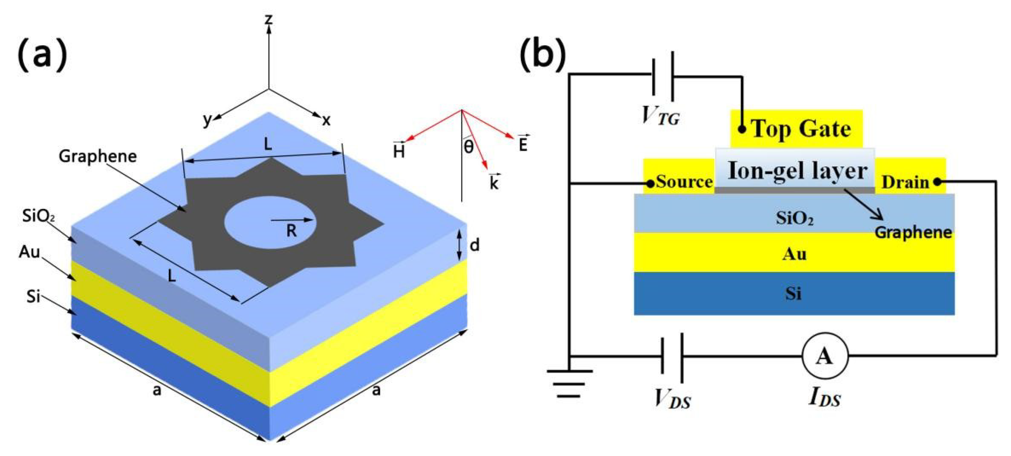
A diagrammatic sketch of our square-square-circle graphene array is shown in Figure 1a. With silicon as the base, gold, silicon dioxide, and graphene were added layer by layer in order. Here, we set the refractive index of Si and the relative permittivity of SiO2 to 3.4 and 3.9 [30,31], respectively. The shape of graphene consists of two overlapping squares with length L and a circle with radius R which is cut out of the center of the square. The thickness of the whole graphene layer tg is 1 nm. The other parameters a, d, and θ represent the period of the array, the thickness of SiO2, and angle of incident light, respectively.
It is known because of Equation (1) that we can adjust the surface conductivity of graphene by changing the Fermi energy. In the mid-infrared and terahertz bands, gate dielectrics such as indium-tinoxide [32,33], monolayer MoS2 [34], 2D electron gas [35,36], and ion-gel [37,38] have been explored in large quantities. At present, the Fermi energy of graphene can be increased by low top gate voltage. The most effective dielectric is an ion-gel with high capacitance. Because of its good mechanical flexibility, fatigue stability, and excellent electrochemical and thermal stability, it can be compatible with tunable graphene plasmonic devices on various substrates [39]. The structure diagram of the ion-gel top gate which can be used to control the Fermi energy of graphene is shown in Figure 1b. The ion-gel layer, which induces carrier concentration and allows the absorber to enter the terahertz band [40,41,42], is inserted between the graphene and gold electrodes.
The Kubo formula, which is made up of interband and intraband transitions, can describe the surface conductivity of graphene σ [30,43]. In the terahertz region, the intraband transition plays a major role as EF >> KBT, where KB and T are the Boltzmann constant and temperature, respectively [44]. Hence, the surface conductivity of graphene σ which is similar to the Drude-like model [45,46,47,48] can be expressed as
where e, ħ, ω, EF, and τ are the electron charge, reduced Plank’s constant, frequency of incident light, Fermi energy, and relaxation time, respectively [49]. In addition, the permittivity of graphene is isotropic in the plane of the thin plate and non-dispersive out of the plane, which can be described in diagonal tensor form using [50,51,52]
where ε0 is the permittivity of a vacuum.
In the simulation, we used the finite-difference time-domain (FDTD Solutions, Lumerical Inc., Vancouver, BC, Canada) method to obtain the data. We set periodic boundary conditions in the x and y directions, respectively. In the z direction of the incident plane wave propagation, perfectly matched layers were utilized. Then, the absorption can be expressed as follows: A(ω) = 1 − R(ω) − T(ω), where R(ω) = |S11(ω)|2 and T(ω) = |S21(ω)|2, gained by S-parameters, are reflection and transmission, respectively. Therefore, the perfect absorption can be discerned by reducing reflection and transmission to zero. In our structure, we set the thickness of the gold layer to 550 nm, which is larger than the skin depth of electromagnetic waves [53]. Hence, transmission can be effectively eliminated.
3. Simulation Results and Discussions
At L = 1000 nm, d = 4200 nm, R = 400 nm, θ = 0°, EF = 0.9 eV, and τ = 0.9 ps, the simulated absorption spectra of the absorber under different periods are plotted in Figure 2. Here, we can see that the resonance wavelength has a blue shift and the absorption peak is almost unchanged with the incremental period. In other words, the period has a great influence on the resonance wavelength but less on the absorption peak. The symmetry of the perfect metamaterial absorber design keeps the absorption almost unchanged with various periods [54]. The inserts indicate the distributions of the electric field (|E|) at a = 2200 nm. It can be clearly seen that the electric field is localized at both ends of the structure, which is caused by the strong electric dipole resonance. This resonance can effectively catch the energy of light and produces enough time to eliminate the ohm loss in graphene. In addition, the reflection of gold reduces transmission to zero, which promotes perfect absorption.
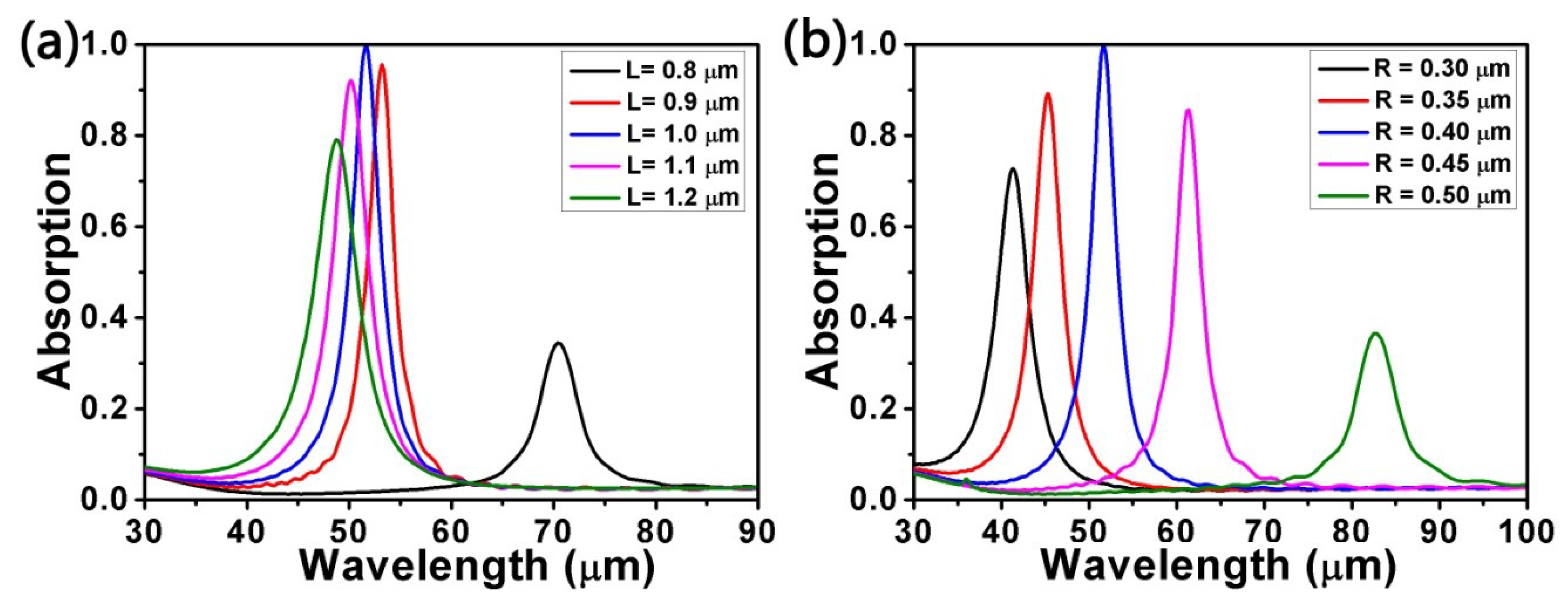
Here, we analyze the influence of different lengths L of the square on the absorption with a = 2200 nm, d = 4200 nm, R = 400 nm, θ = 0°, EF = 0.9 eV, and τ = 0.9 ps. As shown in Figure 3a, as the length L of the square rises from 0.8 μm to 1.2 μm, the resonance wavelength moves to a shorter wavelength, that is, a blue shift occurs. However, the value of the absorption peak experiences a different situation: rising and falling can be observed for L < 1.0 μm and L > 1.0 μm, respectively. That is to say, when L = 1.0 μm, the absorption is nearly perfect. As a result of the impedance matching condition [19] of the structure which is partially up to the parameter L, we can change the absorption peak. Hence, we observe a higher impedance matching condition as L rises. Then, an almost perfect impedance matching condition is gained when L = 1.0 μm. Nevertheless, if we continue to increase L, the impedance will mismatch.
To learn more about the influence of structural parameters on the absorption, we also considered how different radii R of the circle impacted the absorption with L = 1000 nm, d = 4200 nm, a = 2200 nm, θ = 0°, EF = 0.9 eV, and τ = 0.9 ps, as seen in Figure 3b. It is obvious that when R is raised from 0.30 μm to 0.50 μm at intervals of 0.05 μm, the resonance wavelength undergoes a red shift and the absorption goes through a process of increasing initially and then decreasing. Owing to the almost perfect impedance matching condition, the absorption peak reaches a maximum. The above simulation results also illustrate the fact that we can modulate the spectral responses in a way that optimizes the structural parameters L and R.
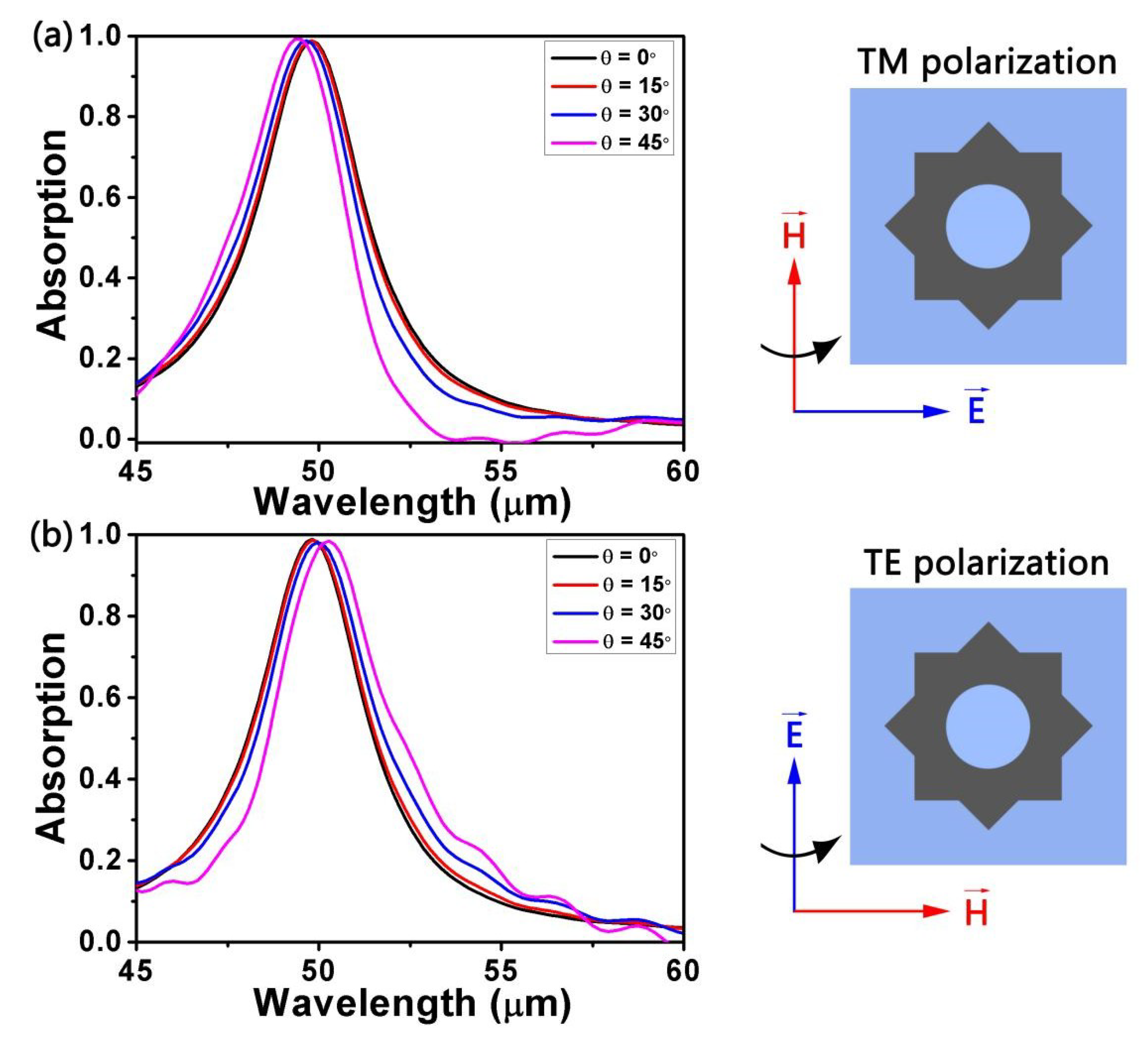
Next, we discuss the impact of different incident angles θ on absorption under TM-polarization and TE-polarization, respectively. TM- and TE-polarization represent the direction of the incidence electric field along the x and y axes, respectively. The other parameters were set as L = 1000 nm, d = 4200 nm, R = 400 nm, a = 2200 nm, EF = 0.9 eV, and τ = 0.9 ps. From Figure 4, it can clearly be seen that in any polarization state, the absorption rates slightly increase or decrease with the incremental incident angle θ because of the varying reflectivity. However, in general, they remain above 0.95. The difference between TM polarization and TE polarization is that the resonance wavelength of the former is blue-shifted and the latter is red-shifted.
As is known, Fermi energy EF, which can be regulated by applying a gate voltage and by means of chemical doping, has a deep influence on the surface conductivity of graphene. The connection between Fermi energy EF and the gate voltage V can be expressed [55] as EF = ħVf (πε0εrV/(ets)), where Vf, ε0, εr, and ts are the Fermi velocity of graphene, the permittivity of a vacuum, the permittivity of the ion-gel and the thickness of the ion-gel, respectively. Therefore, we evaluated the effect of different Fermi energy values on absorption, as seen in Figure 5a. The other parameters were set as L = 1000 nm, d = 4200 nm, R = 400 nm, a = 2200 nm, θ = 0°, and τ = 0.9 ps. We can clearly see that the resonance wavelength experiences a blue shift and the wavelength peak first increases and then decreases with incremental Fermi energy. In Figure 5b we give the functional relationship between Fermi energy and the resonance wavelength. Obviously, there is almost a linear relationship between them. In order to better comprehend this, we propose a physical mechanism involving the charge carrier rising in number with incremental Fermi energy, which contributes to a stronger surface plasmon resonance (SPR) excitation [56,57]. The SPR reaches a maximum as the value of the Fermi energy is 0.9 eV. However, if the Fermi energy continues to increase on the basis of 0.9 eV, the resonance wavelength will depart from the strong SPR region. This is the reason why the wavelength peak increases first and then decreases with incremental Fermi energy.
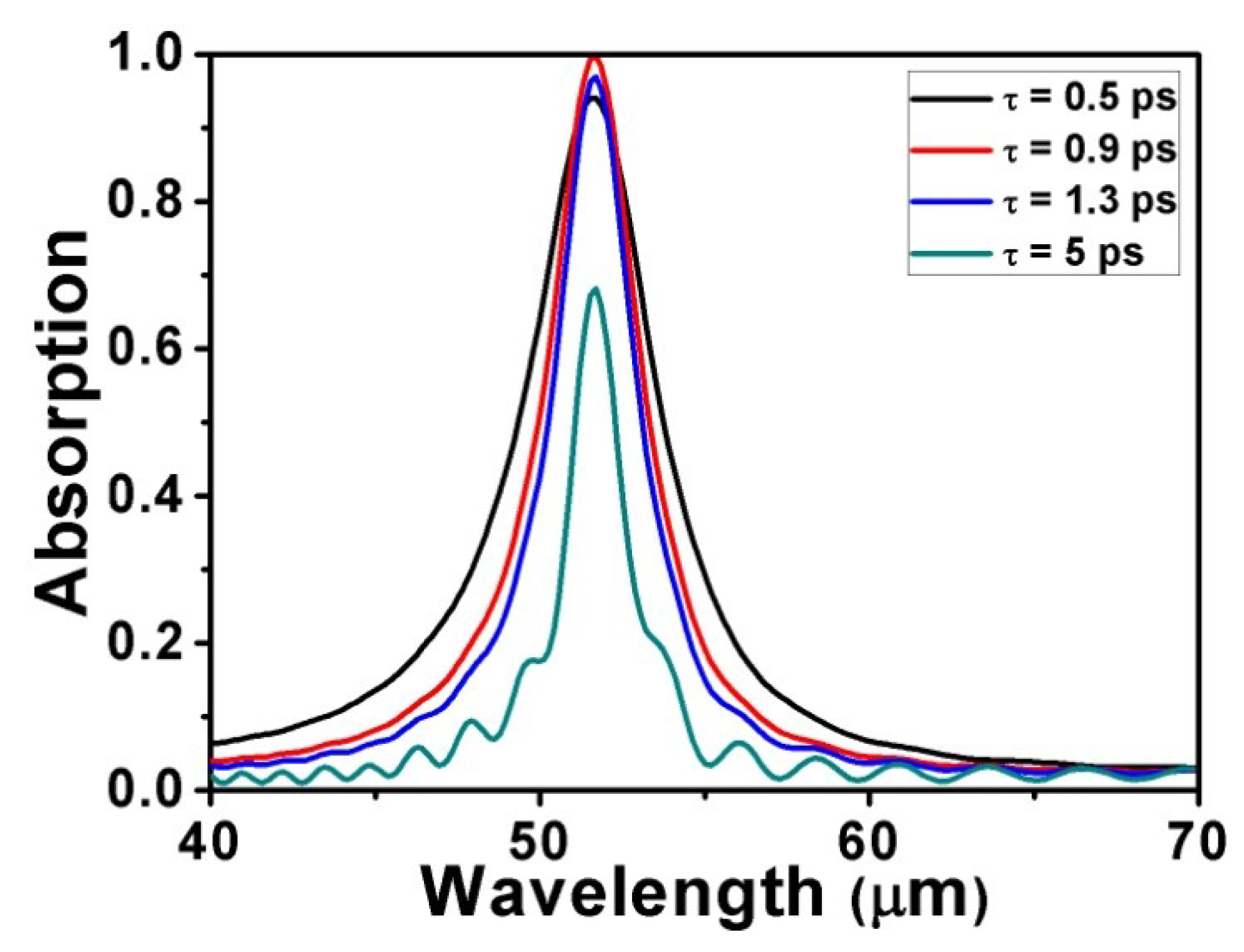
The formula τ = EF·μ/(eVF2), with the Fermi energy EF = 0.9 eV, the Fermi velocity VF = 106 m/s, and the carrier mobility μ = 1 m2/Vs, can be used to describe the relaxation time for graphene. The carrier mobility available can be enhanced by the placement of organic molecules on graphene, thus increasing the relaxation time [58]. As shown in Figure 6, the spectra show changes in absorption at different relaxation times with L = 1000 nm, d = 4200 nm, R = 400 nm, a = 2200 nm, EF = 0.9 eV, and θ = 0°. It is significant that the absorption peak rises when the relaxation time increases from 0.4 eV to 1 eV, while the absorption peak declines when the relaxation time increases from 1 eV to 1.2 eV. There is no doubt that when the relaxation time is equal to 1 eV, the peak is at its maximum. The reason for this phenomenon is that the charge carriers, which are conducive to plasma oscillation absorption, reach the saturation state when the relaxation time is equal to 1 eV [56,59]. If the relaxation time keeps increasing, most energy will be reflected, and the absorption will decrease. Hence, the absorption is no longer nearly perfect.
In order to better evaluate the sensing performance of the structure, we simulated the spectra as the surrounding refractive index n changes. The other parameters were set as L = 1000 nm, d = 4200 nm, R = 400 nm, a = 2200 nm, θ = 0°, EF = 0.9 eV, and τ = 0.9 ps. As shown in Figure 7, it is clear that when n is increased from 1.302 to 1.352 at intervals of 0.01, the absorption peak remains almost unchanged, but the resonance wavelength experiences a red shift. In other words, the surrounding refractive index n has a significant effect on the resonance wavelength but little on the absorption peak. This also indicates the fact that the structure is sensitive to changes in the surrounding refractive index. Furthermore, the absorption peak remains nearly always perfect. Hence, we can say that the structure can be applied to the sensors.
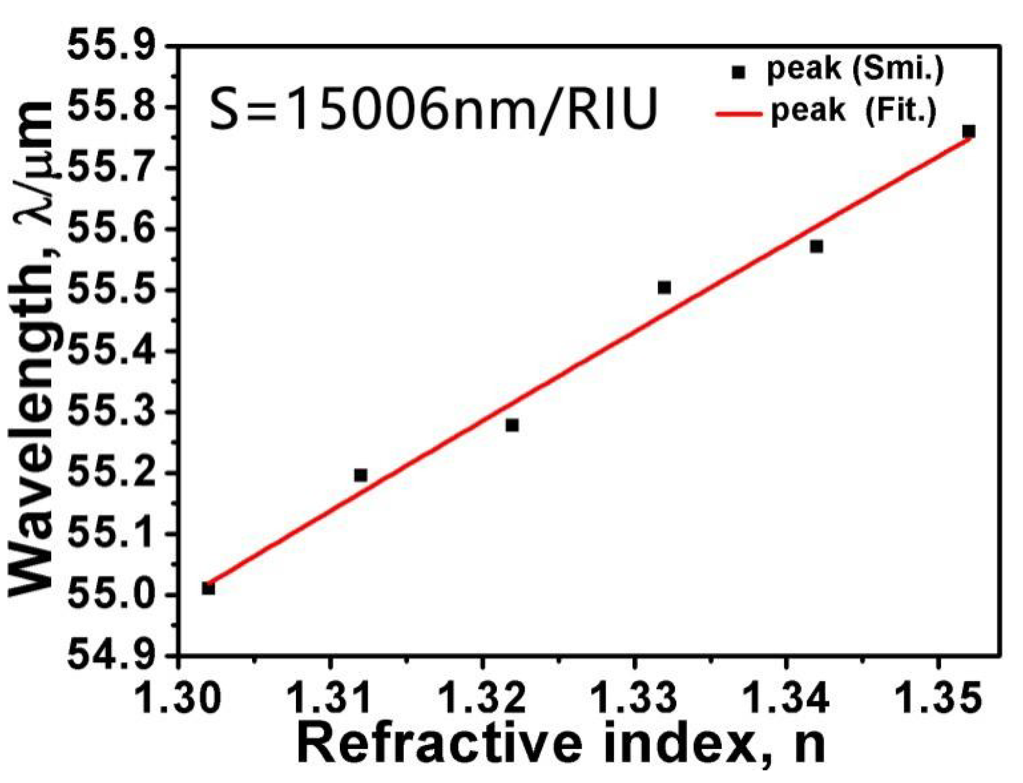
As is known, the sensitivity S and the figure of merit FOM can be used to define the sensing property [60]. The sensitivity can be stipulated as S = ∆λ/∆n and the figure of merit can be expressed as FOM = S/FWHM. Here, ∆λ and ∆n are the change values of resonance wavelength and surrounding refractive index. FWHM is the full width at half maximum of absorption. In Figure 8, we illustrate the relationship between the surrounding refractive index n and the resonance wavelength. Each black dot corresponds to simulated data and the red line is the linear fit. The slope of the red line is expressed as the value of sensitivity S. As Figure 8 shows, the sensitivity S is approximately 15,006 nm/RIU. According to our formula, we obtain FOM = 4.19. Using previously published works on absorbers [59,60,61,62,63,64,65,66], Table 1 provides a comparison of their sensitivity. Compared with these sensors, we can see that the proposed structure has better sensing performance. Therefore, the structure we have proposed can be used as a sensor detector to detect changes in the surrounding environment.
4. Discussion
In this study, we analyzed the optical performance of a periodical tunable plasmonic perfect metamaterial absorber based on a square-square-circle graphene array that we proposed in the terahertz region, by FDTD. Simulated results revealed that we can change the structural parameters to tune the absorption peak and the resonance wavelength of the absorber due to the impedance matching condition. Furthermore, on account of the surface plasmon resonance, the spectra of the absorber can be adjusted by the Fermi energy EF. Additionally, relaxation time may only be used for controlling the absorption intensity because of the little effect on the resonance wavelength. Finally, simulation of the spectra as the surrounding refractive index n changes can produce a sensitivity S of the structure of up to 15006 nm/RIU, which means that it is beneficial for a sensor detector to detect changes in the surrounding environment. Consequently, the absorber we proposed is beneficial to sensors and detectors in the terahertz region.
Author Contributions
Conceptualization, Z.Y., J.C., and C.C.; data curation, Z.Y., J.C., and C.C.; formal analysis, Z.Y., J.C., C.C., X.C., Z.Z., Y.J., X.Y., and S.X.; methodology, Z.Y., J.C., and W.L.; resources, Z.Y.; software, X.Y., W.L., and P.W.; data curation, Z.Y.; writing—original draft preparation, Z.Y.; writing—review and editing, Z.Y., J.C., and C.C.
Funding
This research was funded by the National Natural Science Foundation of China (NNSFC) (51606158, 11604311, and 11704223), the Natural Science Foundation of Fujian Province (2018J05008 and JZ160459), the Sichuan Science and Technology Program (2018GZ0521), the Longshan Academic Talent Research Supporting program of SWUST (18lzx506), the Postgraduate Innovation Fund Project by the Southwest University of Science and Technology (18ycx034), and the Undergraduate Innovation Fund Project by Southwest University of science and Technology (cx18-060).
Conflicts of Interest
The authors declare no conflict of interest.
References
- Novoselov, K.S.; Geim, A.K.; Morozov, S.V.; Jiang, D.; Zhang, Y.; Dubonos, S.V.; Grigorieva, I.V.; Firsov, A.A. Electric Field Effect in Atomically Thin Carbon Films. Science 2004, 306, 666–669. [Google Scholar] [CrossRef] [PubMed] [Green Version]
- Zhao, X.X.; Yang, H.; Li, S.H.; Cui, Z.M.; Zhang, C.R. Synthesis and theoretical study of large-sized Bi4Ti3O12 square nanosheets with high photocatalytic activity. Mater. Res. Bull. 2018, 107, 180–188. [Google Scholar] [CrossRef]
- Lin, H.; Ye, X.; Chen, X.F.; Zhou, Z.G.; Yi, Z.; Niu, G.; Yi, Y.G.; Hua, Y.T.; Hua, J.J.; Xiao, S.Y. Plasmonic absorption enhancement in grapheme circular and Elliptical disk arrays. Mater. Res. Express 2019, 6, 045807. [Google Scholar] [CrossRef]
- Zheng, C.X.; Yang, H.; Cui, Z.M.; Zhang, H.M.; Wang, X.X. A novel Bi4Ti3O12/Ag3PO4 heterojunction photocatalyst with enhanced photocatalytic performance. Nanoscale Res. Lett. 2017, 12, 608. [Google Scholar] [CrossRef] [PubMed]
- Zhang, Q.B; Liao, J.; Liao, M.; Dai, J.Y.; Ge, H.L.; Duan, T.; Yao, W.T. One-dimensional Fe7S8@C nanorods as anode materials for high-rate and long-life lithium-ion batteries. Appl. Surf. Sci. 2019, 473, 799–806. [Google Scholar] [CrossRef]
- Luo, X.; Zhai, X.; Wang, L.L.; Lin, Q. Enhanced dual-band absorption of molybdenum disulfide using plasmonic perfect absorber. Opt. Express 2018, 26, 11658–11666. [Google Scholar] [CrossRef] [PubMed]
- Cen, C.L.; Liu, L.; Zhang, Y.B.; Chen, X.F.; Zhou, Z.G.; Yi, Z.; Ye, X.; Tang, Y.J.; Yi, Y.G.; Xiao, S.Y. Tunable absorption enhancement in periodic elliptical hollow graphene arrays. Opt. Mater. Express 2019, 9, 706–716. [Google Scholar] [CrossRef]
- Ferguson, B.; Zhang, X.C. Materials for terahertz science and technology. Nat. Mater. 2002, 1, 26–33. [Google Scholar] [CrossRef]
- Cen, C.; Lin, H.; Huang, J.; Liang, C.; Chen, X.; Tang, Y.; Yi, Z.; Ye, X.; Liu, J.; Yi, Y.; et al. A Tunable Plasmonic Refractive Index Sensor with Nanoring-Strip Graphene Arrays. Sensors 2018, 18, 4489. [Google Scholar] [CrossRef]
- Cen, C.; Chen, J.; Liang, C.; Huang, J.; Chen, X.; Tang, Y.; Yi, Z.; Xu, X.; Yi, Y.; Xiao, S. Plasmonic absorption characteristics based on dumbbell-shaped graphene metamaterial arrays. Physica E 2018, 103, 93–98. [Google Scholar] [CrossRef] [Green Version]
- Wang, B.Y.; Zeng, Q.D.; Xiao, S.Y.; Xu, C.; Xiong, L.B.; Lv, H.; Du, J.; Yu, H.Q. Low-power, ultrafast, and dynamic all-optical tunable plasmon induced transparency in two stub resonators side-coupled with a plasmonic waveguide system. J. Phys. D Appl. Phys. 2017, 50, 455107. [Google Scholar] [CrossRef] [Green Version]
- Yan, Y.X.; Yang, H.; Zhao, X.X.; Li, R.S.; Wang, X.X. Enhanced photocatalytic activity of surface disorder-engineered CaTiO3. Mater. Res. Bull. 2018, 105, 286–290. [Google Scholar] [CrossRef]
- Cen, C.; Lin, H.; Liang, C.; Huang, J.; Chen, X.; Yi, Z.; Tang, Y.; Duan, T.; Xu, X.; Xiao, S.; et al. Tunable plasmonic resonance absorption characteries-tics in periodic H-shaped graphene arrays. Superlattice Microstruct. 2018, 120, 427–435. [Google Scholar] [CrossRef]
- Ding, P.; Li, Y.; Shao, L.; Tian, X.M.; Wang, J.Q.; Fan, C.Z. Graphene aperture-based metalens for dynamic focusing of terahertz waves. Opt. Express 2018, 26, 28038–28050. [Google Scholar] [CrossRef] [PubMed]
- Bruck, R.; Muskens, O.L. Plasmonic nanoantennas as integrated coherent perfect absorbers on SOI waveguides for modulators and all-optical switches. Opt. Express 2013, 21, 27652–27661. [Google Scholar] [CrossRef] [PubMed]
- Zhao, X.X.; Yang, H.; Cui, Z.M.; Wang, X.X.; Yi, Z. Growth Process and CQDs-modified Bi4Ti3O12 Square Plates with Enhanced Photocatalytic Performance. Micromachines 2019, 10, 66. [Google Scholar] [CrossRef]
- Yi, Z.; Lin, H.; Niu, G.; Chen, X.F.; Zhou, Z.G.; Ye, X.; Duan, T.; Yi, Y.; Tang, Y.J.; Yi, Y.G. Graphene-based tunable triple-band plasmonic perfect metamaterial absorber with good angle-polarization-tolerance. Results Phys. 2019, 13, 102149. [Google Scholar] [CrossRef]
- Li, X.; Chen, X.F.; Yi, Z.; Zhou, Z.G.; Tang, Y.J.; Yi, Y.G. Fabriction of ZnO Nanorods with Strong UV Absorption and Different Hydrophobicity on Foamed Nickel under Different Hydrothermal Conditions. Micromachines 2019, 10, 164. [Google Scholar] [CrossRef] [PubMed]
- Wang, X.; Pang, Z.; Tong, H.; Wu, X.; Bai, X.; Yang, H.; Wen, X.; Qi, Y. Theoretical investigation of subwavelength structure fabrication based onmulti-exposure surface plasmon interference lithography. Results Phys. 2019, 12, 732–737. [Google Scholar] [CrossRef]
- Wang, X.; Tong, H.; Pang, Z.; Zhu, J.; Wu, X.; Yang, H.; Qi, Y. Theoretical realization of three-dimensional nanolattice structure fabrication based on high-order waveguide-mode interference and sample rotation. Opt. Quant. Electron. 2019, 51, 38. [Google Scholar] [CrossRef]
- Zhang, Y.J.; Kuang, Y.Q.; Zhang, Z.D.; Tang, Y.; Han, J.Q.; Wang, R.B.; Cui, J.G.; Hou, Y.L.; Liu, W.Y. High-sensitivity refractive index sensors based on Fano resonance in the plasmonic system of splitting ring cavity-coupled MIM waveguide with tooth cavity. Appl. Phys. A 2019, 125, 13. [Google Scholar] [CrossRef]
- Yi, Z.; Li, X.; Xu, X.B.; Chen, X.; Ye, X.; Yi, Y.; Duan, T.; Tang, Y.J.; Liu, J.W.; Yi, Y.G. Nanostrip-Induced High Tunability Multipolar Fano Resonances in a Au Ring-Strip Nanosystem. Nanomaterials 2018, 8, 0568. [Google Scholar] [CrossRef] [PubMed]
- Zhang, X.W.; Qi, Y.P.; Zhou, P.Y.; Gong, H.H.; Hu, B.B.; Yan, C.M. Refractive Index Sensor Based on Fano Resonances in Plasmonic Waveguide With Dual Side-Coupled Ring Resonators. Photonic Sens. 2018, 8, 367–374. [Google Scholar] [CrossRef]
- Liu, L.; Chen, J.J.; Zhou, Z.G.; Yi, Z.; Ye, X. Tunable absorption enhancement in electric split-ring resonators-shaped graphene array. Mater. Res. Express 2018, 5, 045802. [Google Scholar] [CrossRef]
- Liu, C.; Su, W.Q.; Liu, Q.; Lu, X.L.; Wang, F.M.; Sun, T.; Paul, K.C. Symmetrical dual D-shape photonic crystal fibers for surface plasmon resonance sensing. Opt. Express 2018, 26, 9039–9049. [Google Scholar] [CrossRef] [PubMed]
- Zeng, Y.; Chen, X.F.; Yi, Z.; Yi, Y.G.; Xu, X.B. Fabrication of p-n heterostructure ZnO/Si moth-eye structures: Antireflection, enhanced charge separation and photocatalytic properties. Appl. Surf. Sci. 2018, 441, 40–48. [Google Scholar] [CrossRef]
- Xia, S.X.; Zhai, X.; Wang, L.L.; Wen, S.C. Plasmonically induced transparency in double-layered graphene nanoribbons. Photon. Res. 2018, 6, 692–702. [Google Scholar] [CrossRef]
- Fu, J.H.; Lv, B.; Li, R.J.; Ma, R.Y.; Chen, W.; Wang, Z.F. Excitation of Surface Plasmon Polaritons in an Inhomogeneous Graphene-Covered Grating. Plasmonics 2017, 12, 209–213. [Google Scholar] [CrossRef]
- Wang, J.C.; Song, C.; Hang, J.; Hu, Z.D.; Zhang, F. Tunable Fano resonance based on grating-coupled and graphene-based Otto configuration. Opt. Express 2017, 25, 23880–23892. [Google Scholar] [CrossRef] [PubMed]
- Wang, W.; Kang, C.X.; Liu, X.M.; Qu, S.L. Spin-selected and spin-independent dielectric metalenses. J. Opt. 2018, 20, 095102. [Google Scholar] [CrossRef]
- Chen, J.; Zhang, T.; Tang, C.J.; Mao, P.; Liu, Y.J.; Yu, Y.; Liu, Z.Q. Optical Magnetic Field Enhancement via Coupling Magnetic Plasmons to Optical Cavity Modes. IEEE Photonics Technol. Lett. 2016, 28, 1529. [Google Scholar] [CrossRef]
- Yang, C.S.; Chang, C.M.; Chen, P.H.; Yu, P.; Pan, C.L. Broadband terahertz conductivity and optical transmission of indium-tin-oxide (ITO) nanomaterials. Opt. Express 2013, 21, 16670–16682. [Google Scholar] [CrossRef] [PubMed]
- Yang, C.S.; Tang, T.T.; Chen, P.H.; Pan, R.P.; Yu, P.; Pan, C.L. Voltage-controlled liquid-crystal terahertz phase shifter with indium–tin–oxide nanowhiskers as transparent electrodes. Opt. Lett. 2014, 39, 2511–2513. [Google Scholar] [CrossRef]
- Deng, X.Y.; Deng, X.H.; Su, F.H.; Liu, N.H.; Liu, J.T. Broadband ultra-high transmission of terahertz radiation through monolayer MoS2. J. Appl. Phys. 2015, 118, 224304. [Google Scholar] [CrossRef]
- Choi, B.R.; Hansen, A.E.; Kontos, T.; Hoffmann, C.; Oberholzer, S.; Belzig, W.; Schonenberger, C.; Akazaki, T.; Takayanagi, H. Shot-noise and conductance measurements of transparent superconductor/two-dimensional electron gas junctions. Phys. Rev. B 2005, 72, 024501. [Google Scholar] [CrossRef]
- Sensale-Rodriguez, B.; Fang, T.; Yan, R.; Kelly, M.M.; Jena, D.; Liu, L.; Xing, H. Unique prospects for graphene-based terahertz modulators. Appl. Phys. Lett. 2011, 99, 113104. [Google Scholar] [CrossRef] [Green Version]
- Fang, Z.; Thongrattanasiri, S.; Schlather, A.; Liu, Z.; Ma, L.; Wang, Y.; Ajayan, P.M.; Nordlander, P.; Halas, N.J.; García de Abajo, F.J. Gated tunability and hybridization of localized plasmons in nanostructured graphene. ACS Nano 2013, 7, 2388–2395. [Google Scholar] [CrossRef] [PubMed]
- Fang, Z.; Wang, Y.; Schlather, A.E.; Liu, Z.; Ajayan, P.M.; García de Abajo, F.J.; Nordlander, P.; Zhu, X.; Halas, N.J. Active tunable absorption enhancement with graphene nanodisk arrays. Nano Lett. 2013, 14, 299–304. [Google Scholar] [CrossRef] [PubMed]
- Hu, H.; Zhai, F.; Hu, D.; Li, Z.; Bai, B.; Yang, X.; Dai, Q. Broadly tunable graphene plasmons using an ion-gel top gate with low control voltage. Nanoscale 2015, 7, 19493–19500. [Google Scholar] [CrossRef]
- Das, A.; Pisana, S.; Chakraborty, B.; Piscanec, S.; Saha, S.K.; Waghmare, U.V.; Novoselov, K.S.; Krishnamurthy, H.R.; Geim, A.K.; Ferrari, A.C.; et al. Monitoring dopants by Raman scattering in an electrochemically top-gated graphene transistor. Nat. Nanotechnol. 2008, 3, 210–215. [Google Scholar] [CrossRef] [Green Version]
- Cho, J.H.; Lee, J.; Xia, Y.; Kim, B.S.; He, Y.; Renn, M.J.; Lodge, T.P.; Frisbie, C.D. Printable ion-gel gate dielectrics for low-voltage polymer thin-film transistors on plastic. Nat. Mater. 2008, 7, 900–906. [Google Scholar] [CrossRef] [PubMed]
- Ju, L.; Geng, B.; Horng, J.; Girit, C.; Martin, M.; Hao, Z.; Bechtel, H.A.; Liang, X.; Zettl, A.; Shen, Y.R.; et al. Graphene plasmonics for tunable terahertz metamaterials. Nat. Nanotechnol. 2011, 6, 630–634. [Google Scholar] [CrossRef] [PubMed]
- Liu, Z.; Liu, G.; Huang, S.; Liu, X.; Pan, P.; Wang, Y.; Gu, G. Multispectral spatial and frequency selective sensing with ultra-compact cross-shaped antenna plasmonic crystals. Sens. Actuators B Chem. 2015, 215, 480–488. [Google Scholar] [CrossRef]
- Zheng, B.; Xu, S.Y.; Lin, L.; Wang, Z.Z.; Feng, Z.H.; Zheng, Z.Q. Plasmon enhanced near-infrared quantum cutting of KYF4:Tb3+,Yb3+ doped with Ag nanoparticles. Opt. Lett. 2015, 40, 2630–2633. [Google Scholar] [CrossRef]
- Xiong, Z.W.; Cao, L.H. Red-ultraviolet photoluminescence tuning by Ni nanocrystals in epitaxial SrTiO3 matrix. Appl. Surf. Sci. 2018, 445, 65–70. [Google Scholar] [CrossRef]
- Neto, A.C.; Guinea, F.; Peres, N.; Novoselov, K.S.; Geim, A.K. The electronic properties of grapheme. Rev. Mod. Phys. 2009, 81, 109–162. [Google Scholar] [CrossRef]
- Shi, X.L.; Ma, L.J.; Zhang, Z.D.; Tang, Y.; Zhang, Y.J.; Han, J.Q.; Sun, Y.Q. Dual Fano resonance control and refractive index sensors based on a plasmonic waveguide-coupled resonator system. Opt. Commun. 2018, 427, 326–330. [Google Scholar] [CrossRef]
- Yang, Z.J.; Zhao, Q.; Deng, Y.H.; Zhang, D.; He, J. Efficient second harmonic generation in gold-silicon core-shell nanostructures. Opt. Express 2018, 26, 5835–5844. [Google Scholar] [CrossRef] [PubMed]
- Yi, Z.; Xu, X.B.; Kang, X.L.; Zhao, Y.L.; Zhang, S.L.; Yao, W.T.; Yi, Y.G.; Luo, J.S.; Wang, C.Y.; Yi, Y.; et al. Fabrication of well-aligned ZnO@Ag nanorod arrayswith effective charge transfer for surface-enhanced Raman scattering. Surf. Coat. Technol. 2017, 324, 257–263. [Google Scholar] [CrossRef]
- Gao, W.; Shu, J.; Qiu, C.; Xu, Q. Excitation of plasmonic waves in graphene by guided-mode resonances. ACS Nano 2012, 6, 7806. [Google Scholar] [CrossRef]
- Zeng, C.; Guo, J.; Liu, X.M. High-contrast electro-optic modulation of spatial light induced by graphene-integrated Fabry-Pérot microcavity. Appl. Phys. Lett. 2014, 105, 666. [Google Scholar] [CrossRef]
- Xia, S.X.; Zhai, X.; Wang, L.L.; Lin, Q.; Wen, S.C. Excitation of crest and trough surface plasmon modes in in-plane bended graphene nanoribbons. Opt. Express 2016, 24, 427–436. [Google Scholar] [CrossRef]
- Di, L.; Yang, H.; Xian, T.; Chen, X.J. Facile synthesis and enhanced visible-light photocatalytic activity of novel p-Ag3PO4/n-BiFeO3 heterojunction composites for dye degradation. Nanoscale Res. Lett. 2018, 13, 257. [Google Scholar] [CrossRef]
- Xiong, Z.; Cao, L. Interparticle spacing dependence of magnetic anisotropy and dipolar interaction of Ni nanocrystals embedded in epitaxial BaTiO3 matrix. Ceram. Int. 2018, 44, 8155–8160. [Google Scholar] [CrossRef]
- Zhang, Y.; Feng, Y.; Zhu, B.; Zhao, J.; Jiang, T. Graphene based tunable metamaterial absorber and polarization modulation in terahertz frequency. Opt. Express 2014, 22, 22743–22752. [Google Scholar] [CrossRef]
- Wang, X.X.; Bai, X.L.; Pang, Z.Y.; Yang, H.; Qi, Y.P.; Wen, X.L. Surface-enhanced Raman scattering effect of a composite structure with gold nano-cubes and gold film separated by Polymethylmethacrylate film. Acta Phys. Sin. 2019, 68, 037301. [Google Scholar]
- Pang, Z.Y.; Tong, H.; Wu, X.X.; Zhu, J.K.; Wang, X.X.; Yang, H.; Qi, Y.P. Theoretical study of multiexposure zeroth-order waveguide mode interference lithography. Opt. Quant. Electron. 2018, 50, 335. [Google Scholar] [CrossRef]
- Dai, J.Y.; Li, J.J.; Zhang, Q.B.; Liao, M.; Duan, T.; Yao, W.T. Co3S4@C@MoS2 microstructures fabricated from MOF template as advanced lithium-ion battery anode. Mater. Lett. 2019, 236, 483–486. [Google Scholar] [CrossRef]
- Xiao, W.; Wang, Z.; Zhang, Y.; Fang, R.; Yuan, Z.; Miao, C.; Yan, X.M.; Jiang, Y. Enhanced performance of P (VDF-HFP)-based composite polymer electrolytes doped with organic-inorganic hybrid particles PMMA-ZrO2 for lithium ion batteries. J. Power Sources 2018, 382, 128–134. [Google Scholar] [CrossRef]
- Li, K.; Ma, X.; Zhang, Z.; Song, J.; Xu, Y.; Song, G. Sensitive refractive index sensing with tunable sensing range and good operation angle-polarization-tolerance using graphene concentric ring arrays. J. Phys. D Appl. Phys. 2014, 47, 405101. [Google Scholar] [CrossRef] [Green Version]
- Le, K.Q.; Ngo, Q.M.; Nguyen, T.K. Nanostructured metal-insulator-metal metamaterials for refractive index biosensing applications: Design, fabrication, and characterization. IEEE J. Sel. Top. Quant. 2016, 23, 6900506. [Google Scholar] [CrossRef]
- Shen, Y.; Zhou, J.; Liu, T.; Tao, Y.; Jiang, R.; Liu, M.; Xiao, G.; Zhu, J.; Zhou, Z.K.; Wang, X.; et al. Plasmonic gold mushroom arrays with refractive index sensing figures of merit approaching the theoretical limit. Nat. Commun. 2013, 4, 2381. [Google Scholar] [CrossRef] [PubMed] [Green Version]
- Huang, C.; Ye, J.; Wang, S.; Stakenborg, T.; Lagae, L. Gold nanoring as a sensitive plasmonic biosensor for on-chip DNA detection. Appl. Phys. Lett. 2012, 100, 893–1631. [Google Scholar]
- Cheng, Y.; Mao, X.S.; Wu, C.; Wu, L.; Gong, R.Z. Infrared non-planar plasmonic perfect absorber for enhanced sensitive refractive index sensing. Opt. Mater. 2016, 53, 195–200. [Google Scholar] [CrossRef]
- Li, R.; Wu, D.; Liu, Y.; Yu, L.; Yu, Z.; Ye, H. Infrared Plasmonic Refractive Index Sensor with Ultra-High Figure of Merit Based on the Optimized All-Metal Grating. Nanoscale Res. Lett. 2017, 12, 1. [Google Scholar] [CrossRef]
- Yong, Z.; Zhang, S.; Gong, C.; He, S. Narrow band perfect absorber for maximum localized magnetic and electric field enhancement and sensing applications. Sci. Rep. 2016, 6, 24063. [Google Scholar] [CrossRef] [PubMed] [Green Version]
Figure 1.
(a) Diagrammatic sketch of a unit cell of the square-square-circle graphene array with its geometric parameters and the polarization and propagation of the light source. (b) Principle geometry of the top grid structure for the operating Fermi energy of graphene. VTG, VDS and IDS express the top gate voltage, the voltage and current flowing between Source and Drain, respectively.

Figure 2.
Absorption spectra for different values of period a. Other parameters remain fixed. The inserts indicate the distributions of the electric field (|E|) at a = 2200 nm.
Figure 2.
Absorption spectra for different values of period a. Other parameters remain fixed. The inserts indicate the distributions of the electric field (|E|) at a = 2200 nm.

Figure 3.
Absorption spectra for (a) different lengths L of the square and (b) different radii R of the circle. Other parameters remain fixed.
Figure 3.
Absorption spectra for (a) different lengths L of the square and (b) different radii R of the circle. Other parameters remain fixed.

Figure 4.
Absorption spectra at different incident angles for (a) transverse magnetic (TM)-polarization and (b) transverse electric (TE)-polarization.
Figure 4.
Absorption spectra at different incident angles for (a) transverse magnetic (TM)-polarization and (b) transverse electric (TE)-polarization.

Figure 5.
(a) Absorption spectra for different Fermi energy (EF) values with other parameters fixed. (b) The relationship between Fermi energy and the resonance wavelength.
Figure 5.
(a) Absorption spectra for different Fermi energy (EF) values with other parameters fixed. (b) The relationship between Fermi energy and the resonance wavelength.

Figure 6.
Absorption spectra for different relaxation times with other parameters fixed.

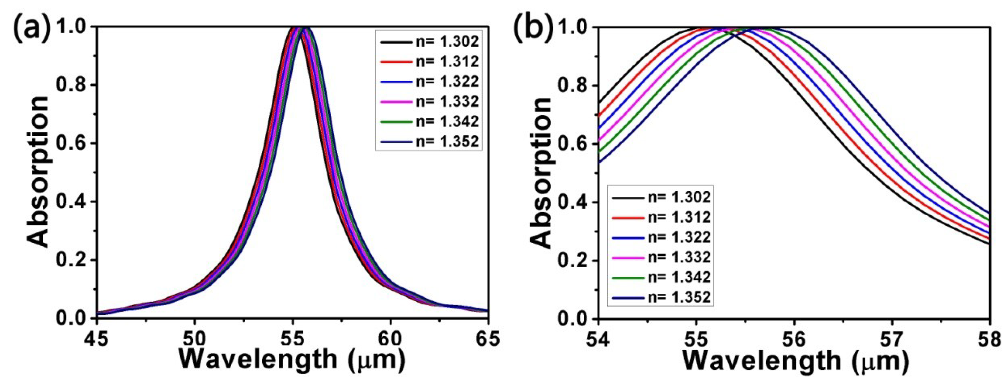
Figure 7.
(a) Absorption spectra for different values of surrounding refractive index n. Other parameters are unchanged. (b) Local details of absorption peaks.
Figure 7.
(a) Absorption spectra for different values of surrounding refractive index n. Other parameters are unchanged. (b) Local details of absorption peaks.

Figure 8.
Simulated resonance wavelengths (black spots) and linear fit (red line) as a function of different values of surrounding refractive index n.
Figure 8.
Simulated resonance wavelengths (black spots) and linear fit (red line) as a function of different values of surrounding refractive index n.


Table 1.
Sensitivity performance comparison between different absorber designs proposed in previous publications.
© 2019 by the authors. Licensee MDPI, Basel, Switzerland. This article is an open access article distributed under the terms and conditions of the Creative Commons Attribution (CC BY) license (http://creativecommons.org/licenses/by/4.0/).
Share and Cite
MDPI and ACS Style
Yi, Z.; Chen, J.; Cen, C.; Chen, X.; Zhou, Z.; Tang, Y.; Ye, X.; Xiao, S.; Luo, W.; Wu, P. Tunable Graphene-based Plasmonic Perfect Metamaterial Absorber in the THz Region. Micromachines 2019, 10, 194. https://doi.org/10.3390/mi10030194
AMA Style
Yi Z, Chen J, Cen C, Chen X, Zhou Z, Tang Y, Ye X, Xiao S, Luo W, Wu P. Tunable Graphene-based Plasmonic Perfect Metamaterial Absorber in the THz Region. Micromachines. 2019; 10(3):194. https://doi.org/10.3390/mi10030194
Chicago/Turabian StyleYi, Zao, Jiajia Chen, Chunlian Cen, Xifang Chen, Zigang Zhou, Yongjian Tang, Xin Ye, Shuyuan Xiao, Wei Luo, and Pinghui Wu. 2019. "Tunable Graphene-based Plasmonic Perfect Metamaterial Absorber in the THz Region" Micromachines 10, no. 3: 194. https://doi.org/10.3390/mi10030194
Note that from the first issue of 2016, this journal uses article numbers instead of page numbers. See further details here.