
Thermally-Induced Deformations and Warpages of Flip-Chip and 2.5D IC Packages Measured by Strain Gauges

Department of Mechanical Engineering, Chang Gung University, Kwei-Shan, Tao-Yuan 333, Taiwan
*
Author to whom correspondence should be addressed.
Materials 2021, 14(13), 3723; https://doi.org/10.3390/ma14133723
Submission received: 24 May 2021
/
Revised: 30 June 2021
/
Accepted: 30 June 2021
/
Published: 2 July 2021
(This article belongs to the Special Issue Simulation and Reliability Assessment of Advanced Packaging)
Abstract
:The thermal warpage problems in integrated circuit (IC) packaging exist in both flip-chip and two-and-a-half dimensional integrated circuits (2.5D IC) packages during manufacturing processes and thermal cycling service. This study proposes a simple and easy-to-use strain gauge measurement associated with a beam model theory to determine the thermally induced deformations and warpages of both packages. First, validation and limitations of the beam model theory are presented. Then, the thermally induced out-of-plane deformations for both packages are well described by the finite element method (FEM) simulation with a good consistency to full-field shadow moiré experimental results. The strain gauge measurements were implemented experimentally, and the thermal strain results were found to be well consistent with validated FEM ones. As a result, out-of-plane thermal deformations and warpages of the packages, calculated from the beam model theory with extracted curvature data from the strain gauge, were in reasonably good agreement with those from FEM analysis and shadow moiré measurements. Therefore, the strain gauge method of featuring point strain measurement combined with the beam model theory proved feasible in determining the thermal deformations and warpages of both IC packages.
1. Introduction
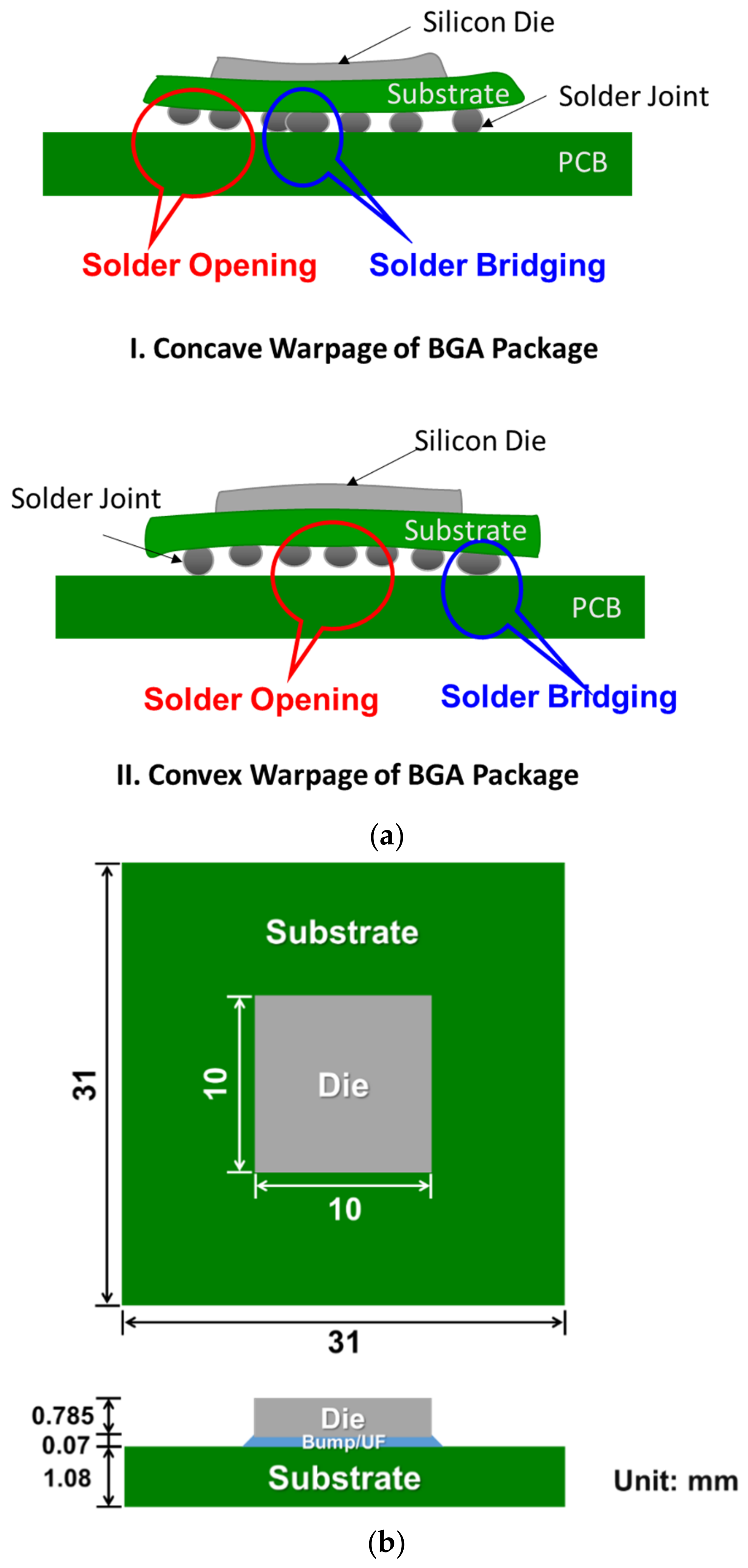
The flip-chip packages and the two-and-a-half dimensional integrated circuits (2.5D IC) packages are popularly used in advanced integrated circuits (IC) packaging [1,2,3]. However, those packages suffer from thermal warpage problems, which may cause solder joint defects, shown in Figure 1a, during manufacturing processes and thermal cycling service due to mismatches of coefficients of thermal expansion (CTE) between the inherent materials [3,4,5,6,7]. Unlike the conventional flip-chip packages, which use a silicon chip to directly bond to the substrate, the 2.5D IC packaging technology uses an additional silicon interposer as a platform to interconnect and integrate heterogeneous or homogeneous chips horizontally and vertically before flip-chip bonding to the substrate [1,3]. Such technology gained more attention in advanced IC packaging for heterogeneous integrations recently. For strain measurement, electrical resistance strain gauges were widely used for point (or local) mechanical strain measurements for more than a century in various engineering applications [8]. Its advantage over other full-field optical methods such as shadow moiré [4,9,10], Twyman–Green interferometry [9,11], or digital image correlation (DIC) [12,13] is that it is easy to use and can provide in-situ and real-time thermal strain measurements, especially for complex printed circuit boards (PCB) during the heating at a solder reflow oven [14]. Some preliminary results of thermal deformations of the 2.5D IC package were presented in an international conference [15]. In this study, the conventional strain gauges were employed for measuring the curvatures of the flip-chip package and the 2.5D IC package reinforced with a metal frame (as shown in Figure 1b,c) under thermal loads. Then, those curvature data were converted to deformations (or warpages) data using a beam model theory. Note that the thermal deformation of the package here is presented by its out-of-plane displacement referred to fixed center point, while the warpage is the out-of-plane displacement of a certain point. Feasibility and validity of this strain gauge method are thoroughly discussed herein by comparing the obtained thermal deformation and warpage results with those from the full-field shadow moiré and the FEM analysis in this study.
2. Methodologies
The methods used in this study for determining the thermal deformations and warpages of the IC packages are briefly illustrated in this section, including the combination of strain gauge and a beam model theory, the finite element analysis, and a shadow moiré measurement.
2.1. Deformation Measurement by Stain Gauges Associated with A Beam Model
The typical strain gauge measurement [8] can be described as
where εa is an apparent strain which is directly obtained from strain gauge measurement system, εt is a true strain which is an actual strain on the measured point of the specimen, Sg is a gauge factor, ΔT is thermal loading, and γg and γw are the temperature coefficients of resistivity of gauge-grid metal material and connected lead wire, respectively. Back-to-back strain gauges were adhered at a specific position on both top and bottom surfaces of the IC package for measuring the thermal strains on the package during heating and cooling processes. The apparent strains on the top and the bottom surfaces (εa,top and εa,bot) of the package can be written individually in terms of the true strains on the top and the bottom surfaces (εt,top and εt,bot) as
The strain data at various temperatures could be further converted into bending strains (εb) and bending curvatures (k) of the IC package by Equations (4) and (5), respectively. Then, the out-of-plane displacement (deformation) of the IC package under different temperatures could be further calculated by Equation (6) with a given curvature and distance x from the center.
where t is the package thickness, and W is the out-of-plane displacement (deformation) at the given distance x with a constant curvature k.
Since the curvature of the package may not be constant across the entire surface of the package, a beam model theory, as shown in Figure 2, with multiple curvatures for the out-of-plane displacement calculation is proposed in this study. This model is based on a beam theory with an assumption of a small deflection. The ki is a constant curvature on the segment i between the length li−1 and li. The k1 represents the curvature of the center segment. The associated equations of an out-of-plane displacement (or deflection) Wi within the segment i are listed [14] as follows:
W0 = 0, x = 0
2.2. FEM Simulation
An isothermal linear FEM analysis was performed to calculate the thermally induced package deformation and warpage due to the CTE mismatch between the inherent materials properties. The schematics of the FEM models are also shown in Figure 3a,b for the flip-chip and the 2.5D IC packages, respectively, with related boundary conditions and meshes in a quarter model. Material mechanical properties used in the finite element analysis are shown in Table 1, in which most data are provided by material vendors. Since the obtained strain data from the FEM analysis were in the x–y coordinate, the transformation of strain vector {ε}x from the x-y coordinate to {ε}1,θ in the 1–2 coordinate with a rotation angle of θ was needed during the data process and is illustrated in Figure 4, in which [T] is a transformation matrix as a function of θ. It is noted that this strain transformation was used for calculating a normal (or axial) strain in the 1-axis direction, such as the diagonal direction of the package or the strain gauge direction during the data process. Then, the FEM simulation results were further used to compare with those from strain gauge measurements in terms of curvatures and from moiré measurement in terms of deformations for both packages. In addition, there were two 2D FEM models—plane stress and axisymmetric models—implemented in this study for validating the beam model theory.
2.3. Shadow Moiré Measurements
The shadow moiré method [4,9,10] is widely used to measure the out-of-plane displacement of the specimens. The systems with the sensitivity of 12.7 μm/fringe and 25.4 μm/fringe were used for the thermal deformation measurement of the flip-chip and the 2.5D IC packages, respectively. An oven or a hot plate were used to heat the specimens and provided thermal loading from room temperature to 260 °C. The present thermal cycling test plus data recording in general took about one hour from room temperature to 260 °C and longer for cooling by natural cooling. Two test samples, a flip-chip package with a size of 31 × 31× 1.94 mm3 and a 2.5D IC package with a size of 55 × 55 × 2.73 mm3 (shown in Figure 1b,c), were tested in the moiré experiments by measuring surfaces on their substrates in this study.
3. Results and Discussion
The obtained results of the flip-chip package and the 2.5D IC package are extensively discussed individually in this section, including the beam model verification, the strain gauge measurement, the moiré measurement, and the FEM analysis.
The Case of Flip-Chip Package
- (a)
- Validation of beam model with FEM simulation
A beam with two curvatures (k1 and k2) over the entire length was considered. A schematic of the out-of-plane displacements of the beam with given constant curvatures k1 and various k2 is shown in Figure 5. The normalized curvature was λ = k2/k1 and the normalized beam length was β = l2/l1. From the beam theory (Equations (7b) and (7c)), W2(l2)λ = 1 and W2(l2)λ, representing the out-of-displacements (warpages) for λ = 1 and any value, respectively, at x = l2, could be described as follows:
It can be also seen from Figure 5 that W2(l2)λ, the out-of-displacement at x = l2, was larger than W2(l2)λ = 1 when λ > 1, otherwise it was smaller. Thus, in order to reduce the warpage of the beam, the λ < 1 had to be selected. That meant the beam with k2 < k1 was preferred. In addition, from Equation (9), the curvature k1 played a more important (or dominant) role than k2 in the value of W2(l2)λ because it had an additional slope term k1l1(l2 − l1) affecting W2(l2)λ. For parametric demonstrations, the normalized W2(l2)λ by the value of W2(l2)λ = 1 is shown as
The above equation could be further expressed in terms of λ and β, as described by
For validation of this beam theory, Equation (11) is plotted against β and λ in Figure 6 and was compared with the results from the plane stress and the axisymmetric models of 2D FEM analyses. It is shown that the results from the beam theory and the plane stress model were very consistent, but they were slightly different from the axisymmetric model, which represented a plate (with a Poisson effect) rather than a beam (without a Poisson effect). Moreover, for λ = 1, the results from the beam theory and the plane stress model were close to those from the axisymmetric model; for λ < 1, they were overestimated, but for λ > 1, they were underestimated. In order to understand this mechanism, curvature distributions for the β = 2 case from the beam theory are plotted in Figure 7 along the entire length of the beam with various values of normalized curvature (λ) in comparison with those from the 2D plane stress and the axisymmetric models of the FEM analyses. It was found that, unlike consistent and constant curvatures (k1 and k2) over each segment between the beam theory and the plane stress model, the axisymmetric model (representing the plate case) gave smaller curvature k1 and non-uniform k2 values as λ < 1. In other words, the out-of-plane displacement (or warpage) caused by smaller curvature k1 and non-uniform k2 resulting from the Poisson effect in the axisymmetric model was lower than that in the beam theory and the plane stress model. As a result, both beam and plane stress models gave an overestimated value of the displacement or the warpage as λ < 1. However, for λ > 1, this was reversed. Furthermore, to examine the detailed warpages, the out-of-displacement of the beam along the entire length of the beam for the β = 2 case is plotted for those three models in Figure 8. It can be also seen that the out-of-plane displacement curves were very consistent for the three models for λ = 1, but the curves from both beam theory and plane stress model started deviating from those in the axisymmetric model with increasing values for λ < 1 and decreasing values for λ > 1. Based on the above observations, it was proven that the beam theory described in Equation (7) coincided with the 2D plane stress model but had some deviations from the 2D axisymmetric model due to the Poisson effect. The question is whether the beam theory can be used for calculating the out-of-displacement of the plate-like IC packages with the curvature data obtained from the strain gauge measurements. That is answered later in this paper.
- (b)
- Validation of FEM simulation with shadow moiré
To verify the result from the 3D FEM analysis, the out-of-plane displacements of the flip-chip package along the diagonal line ac at room temperature (T = 25 °C) and T = 260 °C are shown in Figure 9 from the 3D FEM analysis and the moiré measurement. It can be seen that the 3D FEM model effectively and precisely described the thermal deformation of the flip-chip package based on those consistent results. However, whether the 2D FEM (with axisymmetric model) or the strain gauge measurement associated with the beam model theory can do the same is discussed later.
- (c)
- Implementation of gauge measurement
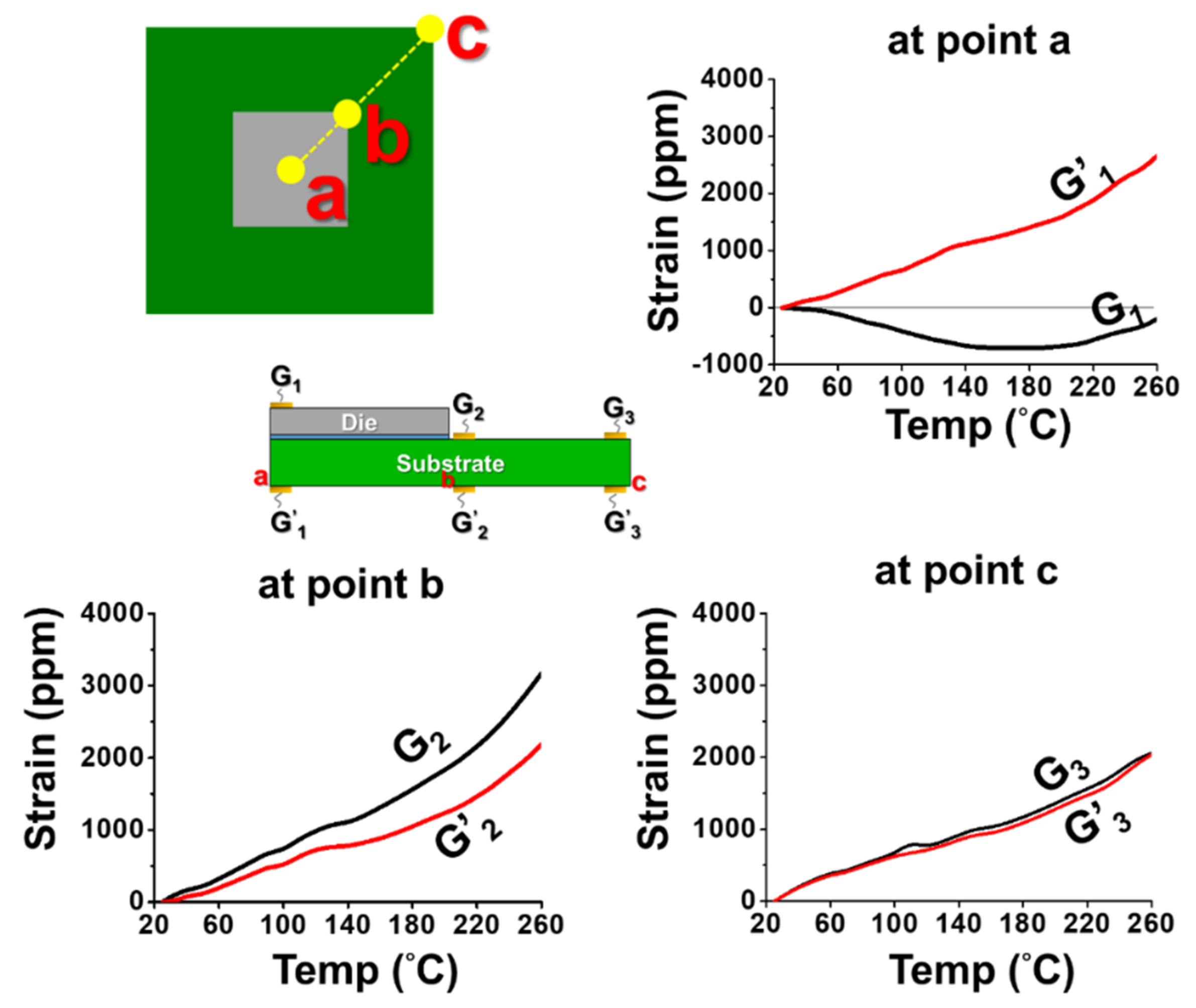
The back-to-back gauges G1/G1′, G2/G2′, and G3/G3′ were attached on the top and the bottom surfaces of the flip-chip package at the points a, b, and c (representing center point, near die corner, and substrate corner points), respectively, for the strain measurement. The measured strain data with various temperatures are shown in Figure 10. The data indicate that the difference of the strain data between the bottom and the top gauges was large at point a (the center point), while it was small at point c (near substrate corner). That meant there existed the bending strains (εb) with a large value at the center point, an intermediate value at the near die corner, and a small value near the substrate corner based on Equation (4). Furthermore, by Equation (5), those bending strain data could be converted to the curvature data, which are shown in Figure 11a, for various temperatures with curvatures ka, kb, and kc at the measured points a, b, and c, respectively. It was found that there existed a kinked point on the curve of ka but not on other curves near T = 120 °C, which was the glass transition temperature (Tg) of the underfill material. This resulted from the elastic modulus (E) of the underfill material with about two orders of magnitude decrease at a temperature above its Tg [5]. Additionally, at this Tg, the curvature on every point on the flip-chip package was almost zero based on the observation of flatness of the package in moiré experiments. Thus, all curvature curves could be further shifted to T = 120 °C with the predefined zero curvature (shown in Figure 11b). It was evident that there existed the apparent value of kb (near the corner of the chip) but with the close zero value of kc near the substrate corner. This was due to the Poisson effect, which was consistent with the case of λ = 0 with the axisymmetric model in Figure 7. Moreover, the curvature data from T = 120 °C cooling to 25 °C in Figure 11b were used to calculate the out-of-plane displacement of the package at room temperature (T = 25 °C) along the diagonal line ac using Equation (7), and this displacement result obtained from the strain gauge was compared with those from moiré and FEM (with 2D axisymmetric and 3D models), as shown in Figure 12. It was shown that, due to an inherent limitation of the beam theory (Equation (7)), the displacements obtained from strain gauge were closer to those of the 2D axisymmetric FEM model than those from moiré and 3D FEM models. Furthermore, the thermally induced warpages of the package at the point c (the corner of the package) from the strain gauge measurement are plotted in Figure 13 against temperature in comparison with those from moiré data and FEM results (with 2D axisymmetric and 3D models). Results also indicated that the gauge result was consistent with the 2D axisymmetric result but was slightly off from results of moiré and 3D FEM models. However, in the engineering applications, the strain gauge measurement associated with the beam model theory was accordingly proved to be feasible and good enough to determine the thermally induced out-of-plane deformations and warpage of the flip-chip packages.
4. The Case of 2.5D IC Package
- (a)
- Validation of FEM simulation
Moiré measurement of the 2.5D IC package with a metal frame under thermal loading from 25 °C to 260 °C in heating and cooling was performed, and its moiré fringe patterns (out-of-plane displacement contours with a sensitivity of 25.4 µm/fringe) are shown in Figure 14 [16]. It was obvious that, during the heating process, the spherically convex shape of the specimen at 25 °C became less warped as the temperature increased and then turned out to be flat at 140 °C. Upon continuous heating, the specimen became concave above 140 °C and increasingly up to 260 °C. On the other hand, the specimen deformed in the reverse way during the cooling process and then came back to the same deformed shape at 25 °C. Such thermal elastic deformations of the package along the diagonal line oa at 25 °C and 260 °C are plotted and shown in Figure 15 in detail in comparison with those from the FEM analysis. The consistent results between moiré and FEM analysis indicated that the FEM model was valid and precise enough to describe the thermal deformations of the 2.5D IC package.
- (b)
- Beam model verification
After the FEM model was validated, this model was then employed for verifying the beam model theory, which was applied to calculate the thermal deformations of the 2.5D IC package with the strain gauge data later. Curvature distribution along the diagonal line oa of the package under thermal loading ΔT = −115 °C (from 140 °C cooling down to 25 °C) from the FEM analysis is shown in Figure 16a with the average curvatures of k1, k2, and k3 over the gauge length at the corresponding segment. These gauge-assumed curvature data extracted from the FEM model were put into the beam model theory as described in Equation (7) to calculate the out-of-plane displacement. The thermally induced out-of-plane displacement of the 2.5D IC package obtained is shown in Figure 16b compared with that from the FEM analysis. The almost identical results of both methods revealed that the method of using the point-wise data of strain gauge associated with the beam model theory was feasible for measuring the thermal deformation of the 2.5D IC package.
- (c)
- Implementation of strain gauge measurement
The strain gauge measurement was further carried out for determining the bending curvatures and deformations of the 2.5D IC package under thermal loading from 140 °C to 25 °C in the cooling process. Note that the strain gauge readings were reset at zero at 140 °C. In Figure 17, the back-to-back strain gauges were attached at the centers of lines AB, BC, and CD along half of a diagonal line with the gauge pairs of G1/G2, G3/G4, and G5/G6, respectively. The axial thermal strains of each reading from those six gauges are also shown in Figure 17 in comparison with those from the FEM simulation. The consistency between both data indicated that the strain gauges could measure the thermal strains of the package. The bending curvature data under this thermal loading were further extracted using Equations (4) and (5) and are shown in Figure 18 in a detailed comparison with the FEM results. Almost identical results revealed that the curvature data for k1, k2, and k3, corresponding to those on lines AB, BC, and CD, increased positively for k2 and k3 but increased negatively for k1 in the cooling process. Their maximum curvatures occurred at 25 °C. The differences of the maximum curvatures between strain gauge measurement and FEM simulation were within 8% (listed in the left table). Moreover, the out-of-plane displacement at 25 °C was plotted using Equation (7) of the beam model theory associated with the curvature data (k1, k2, and k3) from the gauge measurement and is shown in Figure 19 in comparison with those from shadow moiré measurement and FEM simulation. The results indicated that the out-of-plane displacement of the 2.5D IC package from gauge measurement reasonably agreed with the other two with a minor difference. The warpages of the 2.5D IC package at various temperatures are further plotted in Figure 20 from the strain gauge measurement, the shadow moiré measurement, and the FEM simulation. Those results also showed a reasonably good agreement between each other. Overall, this study demonstrated that the strain gauge measurement associated with the beam model theory can be used for characterizing the out-of-plane thermal deformation and warpage of the 2.5D IC package.
- (d)
- Effect of segment curvature variation on warpage
It is interesting to know how the curvature data k1, k2, and k3 at each segment affected the warpage of the 2.5D IC package. The plus and the minus 10% variations of each curvature data in Figure 16a used in plotting displacement using the beam model were analyzed, and the obtained warpage results and their difference are listed in Table 2. Note that k1, k2, and k3 were normalized values and defined as unity for reference. It could be seen that the warpage was the most sensitive to k1, rather than k2 and k3, with increases or decreases of ~15% of warpage value by changing ±10% of k1 values, respectively. This was consistent with the above-mentioned finding that k1, the curvature of the center segment, was a dominant value in the warpage of the packages. Therefore, the precisely defined or measured k1 was more important than the other two (k2 and k3) for the warpage calculation or the measurement of the 2.5D IC package.
- (e)
- Effect of gauge misalignment on warpage
Since the precise measurement of k1 was critical for determining the warpage of the 2.5D IC package, it was desired to understand how the misalignment of k1 gauges affected the warpage. Various angle misalignments (with ±5° and ±10°) of top and bottom strain gauges in the 45° direction in segment AB (the center segment) were analyzed using a beam model for calculating the package warpage through the measurement of k1 curvatures. The results are shown in Table 3, in which the warpage determined from the top and the bottom gauges in the angle of 45° was used as a based (or reference) value. It could be seen that, for ±5° misalignments, the obvious warpage differences occurring at the angle pairs of 50°/50° and 40°/40° were 3.57% and −3.76%, while the other pairs were below 3%. However, for ±10° misalignments, the warpage difference increased by more than double. As a result, as long as the gauge alignment on the top and the bottom surfaces was under control with less than ±5° misalignments, the results of the warpage measurement were acceptable with less than 5% error.
5. Conclusions
This study proposed the strain gauge method associated with a beam model theory for determining the thermally induced deformations and warpages of the flip-chip and the 2.5D IC packages. The beam model theory was thoroughly evaluated in this study, and it was found that the theory coincided with the 2D plane stress model but had some deviations from the 2D axisymmetric model due to the Poisson effect. The finite element method (FEM) resulted with good consistency with the full-field shadow moiré experiment, showing good prediction of thermally induced out-of-plane deformations for both packages. Furthermore, the strain gauge measurement with the beam model theory was actually implemented for both packages. It was found that the obtained thermal strain data were in good agreement with the FEM data. The gauge-determined thermal deformations and warpages of both packages also showed reasonably good agreement with those from the FEM analyses and the shadow moiré measurements. Moreover, the curvature in the center segment of the 2.5D IC package was found to be a dominant value in control of thermal warpages of the package. The gauge misalignment effect was also evaluated and discussed in detail. Overall, it was proven that the strain gauge method of featuring point strain measurement associated with the beam model theory can be feasible for measuring the thermal deformations and warpages of both packages.
Author Contributions
Conceptualization, M.-Y.T., Y.-W.W. and C.-M.L.; Methodology, M.-Y.T., Y.-W.W. and C.-M.L.; Software, Y.-W.W. and C.-M.L.; Validation, M.-Y.T., Y.-W.W. and C.-M.L.; Formal Analysis, Y.-W.W. and C.-M.L.; Investigation, M.-Y.T., Y.-W.W. and C.-M.L.; Resources, M.-Y.T.; Data Curation, Y.-W.W. and C.-M.L.; Writing—Original Draft Preparation, M.-Y.T.; Writing—Review & Editing, M.-Y.T.; Visualization, M.-Y.T.; Supervision, M.-Y.T.; Project Administration, M.-Y.T.; Funding Acquisition, M.-Y.T. All authors have read and agreed to the published version of the manuscript.
Funding
This study was supported by Ministry of Science and Technology, Taiwan under project MOST-108-2221-E-182-045-MY3.
Institutional Review Board Statement
Not applicable.
Informed Consent Statement
Not applicable.
Data Availability Statement
On inquiry, the data presented in this study is available from the authors.
Acknowledgments
Financial support from Ministry of Science and Technology, Taiwan is gratefully acknowledged.
Conflicts of Interest
The authors declare no conflict of interest.
References
- Lau, J.H. Low Cost Flip Chip Technologies; McGraw-Hill: New York, NY, USA, 2000. [Google Scholar]
- Garrou, P. Introduction to 3D Integration; Wiley: Hoboken, NJ, USA, 2008; pp. 1–11. [Google Scholar]
- Lau, J.H. Critical Issues of 3D IC Integrations. In Proceedings of the IMAPS International Symposium on Microelectronics, San Jose, CA, USA, 1–5 November 2009; pp. 585–592. [Google Scholar]
- Tsai, M.-Y.; Chang, H.-Y.; Pecht, M. Warpage Analysis of Flip-Chip PBGA Packages Subject to Thermal Loading. IEEE Trans. Device Mater. Reliab. 2009, 9, 419–424. [Google Scholar] [CrossRef]
- Tsai, M.-Y.; Wang, Y.-W. A Theoretical Solution for Thermal Warpage of Flip-Chip Packages. IEEE Trans. Compon. Packag. Manuf. Technol. 2020, 10, 72–78. [Google Scholar] [CrossRef]
- Zhang, X.; Chai, T.; Lau, J.H.; Selvanayagam, C.S.; Biswas, K.; Liu, S.; Pinjala, D.; Tang, G.; Ong, Y.; Vempati, S.; et al. Development of through silicon via (TSV) interposer technology for large die (21 × 21 mm) fine-pitch Cu/low-k FCBGA package. In Proceedings of the 2009 59th Electronic Components and Technology Conference, San Diego, CA, USA, 26–29 May 2009; pp. 305–312. [Google Scholar]
- Lee, C.-C.; Hung, C.; Cheung, C.; Yang, P.-F.; Kao, C.-L.; Chen, D.-L.; Shih, M.-K.; Chien, C.-L.C.; Hsiao, Y.-H.; Chen, L.-C.; et al. An Overview of the Development of a GPU with Integrated HBM on Silicon Interposer. In Proceedings of the 2016 IEEE 66th Electronic Components and Technology Conference (ECTC), Las Vegas, NV, USA, 31 May–3 June 2016; pp. 1439–1444. [Google Scholar]
- Dally, J.W.; Riley, W.F. Experimental Stress Analysis, 14th ed.; College House Enterprises: Knoxville, TN, USA, July 2006. [Google Scholar]
- Post, D.; Han, B.; Ifju, P. High Sensitivity Moiré Experimental Analysis for Mechanics and Materials; Springer: New York, NY, USA, 1993. [Google Scholar]
- Tsai, M.-Y.; Chen, Y.-C.; Lee, S. Correlation Between Measurement and Simulation of Thermal Warpage in PBGA With Consideration of Molding Compound Residual Strain. IEEE Trans. Compon. Packag. Technol. 2008, 31, 683–690. [Google Scholar] [CrossRef]
- Tsai, M.-Y.; Hsu, C.; Wang, C. Investigation of Thermomechanical Behaviors of Flip Chip BGA Packages During Manufacturing Process and Thermal Cycling. IEEE Trans. Compon. Packag. Technol. 2004, 27, 568–576. [Google Scholar] [CrossRef]
- Park, S.; Dhakal, R.; Joshi, R. Comparative Analysis of BGA Deformations and Strains Using Digital Image Correlation and Moiré Interferometry. In Proceedings of the Sem Annual Conference and Exposition on Experimental and Applied Mechanics, Portland, OR, USA, 7–9 June 2005. [Google Scholar]
- Kim, Y.; Park, A.-Y.; Kao, C.-L.; Su, M.; Black, B.; Park, S. Prediction of deformation during manufacturing processes of silicon interposer package with TSVs. Microelectron. Reliab. 2016, 65, 234–242. [Google Scholar] [CrossRef]
- Liao, M.C.; Huang, P.S.; Lin, Y.H.; Tsai, M.Y.; Huang, C.Y.; Huang, T.C. Measurements of Thermally-induced Cur-vatures and Warpages of Printed Circuit Board During a Solder Reflow Process Using Strain Gauges. Appl. Sci. 2017, 7, 739. [Google Scholar] [CrossRef]
- Tsai, M.Y.; Liu, G.M.; Wang, Y.W. Measurement of Thermally-Induced Curvatures and Warpages of 2.5D Packages by Using Strain Gauges. In Proceedings of the IMPACT 2019, Taipei, Taiwan, 23–25 October 2019. [Google Scholar]
- Tsai, M.-Y.; Liu, C.-M.; Wang, Y.-W.; Liu, H.-Y.; Liu, G.M. Effects of Metal Frame and Adhesive on Thermally-Induced Warpage and Stress of 2.5D Packages: Experimental and Numerical Studies. IEEE Trans. Device Mater. Reliab. 2018, 18, 450–455. [Google Scholar] [CrossRef]
Figure 1.
Schematics of (a) thermal warpage induced solder joint defects, (b) a flip-chip package and (c) a 2.5D IC package with detailed materials and dimensions.
Figure 1.
Schematics of (a) thermal warpage induced solder joint defects, (b) a flip-chip package and (c) a 2.5D IC package with detailed materials and dimensions.


Figure 2.
Schematic of the beam with constant curvatures k1, k2, and k3 at different segments.

Figure 3.
A quarter model and meshes of (a) a flip-chip package and (b) a 2.5D IC package used in the finite element analysis.
Figure 3.
A quarter model and meshes of (a) a flip-chip package and (b) a 2.5D IC package used in the finite element analysis.

Figure 4.
Transformation of strain vector {ε}x from the x–y coordinate to {ε}1,θ in the 1–2 coordinate with a rotation angle of θ.
Figure 4.
Transformation of strain vector {ε}x from the x–y coordinate to {ε}1,θ in the 1–2 coordinate with a rotation angle of θ.

Figure 5.
Schematic of the out-of-plane displacement of the beam with given constant curvatures k1 and various k2 (or various λ = k2/k1).
Figure 5.
Schematic of the out-of-plane displacement of the beam with given constant curvatures k1 and various k2 (or various λ = k2/k1).

Figure 6.
Normalized warpage (W2(l2)λ/W2(l2)λ = 1) vs. normalized beam length (β = l2/l1) for the beam theory (in solid lines) with various values of normalized curvature (λ = k2/k1) compared with the results from the plane stress (in dot points) and the axisymmetric models (in dash lines) of 2D FEM analyses.

Figure 7.
Curvature distributions along the length of the beam for the β = 2 case from the beam theory (in dash lines) with various values of normalized curvature (λ), compared with the results from plane stress (in dash lines) and axisymmetric models (in solid lines) of 2D FEM analyses.
Figure 7.
Curvature distributions along the length of the beam for the β = 2 case from the beam theory (in dash lines) with various values of normalized curvature (λ), compared with the results from plane stress (in dash lines) and axisymmetric models (in solid lines) of 2D FEM analyses.

Figure 8.
Out-of-plane displacement of the beam along the length of the beam for the β = 2 case from the beam theory (in dash lines) with various values of normalized curvature (λ) compared with the results from 2D plane stress (in dash lines) and axisymmetric (in solid lines) models of FEM.
Figure 8.
Out-of-plane displacement of the beam along the length of the beam for the β = 2 case from the beam theory (in dash lines) with various values of normalized curvature (λ) compared with the results from 2D plane stress (in dash lines) and axisymmetric (in solid lines) models of FEM.

Figure 9.
Out-of-plane displacement of the package along the diagonal line ac and with a full field at room temperature (T = 25 °C) and T = 260 °C from the 3D FEM analysis compared with moiré results.
Figure 9.
Out-of-plane displacement of the package along the diagonal line ac and with a full field at room temperature (T = 25 °C) and T = 260 °C from the 3D FEM analysis compared with moiré results.

Figure 10.
The strain data from the back-to-back gauges with various temperatures and with gauges G1/G1′, G2/G2′, and G3/G3′ at the points a, b, and c (representing center point, near die corner, and substrate corner points), respectively, during the strain measurement under thermal loading from 25 °C to 260 °C in heating.

Figure 11.
The curvature data at the points a, b, and c (representing center point, near die corner, and substrate corner points, respectively) with various temperatures from the strain gauge measurement (a) before shift and (b) after shift to 120 °C with the zero curvature.
Figure 11.
The curvature data at the points a, b, and c (representing center point, near die corner, and substrate corner points, respectively) with various temperatures from the strain gauge measurement (a) before shift and (b) after shift to 120 °C with the zero curvature.

Figure 12.
Out-of-plane displacement of the package at room temperature (T = 25 °C) along the diagonal line ac from the strain gauge measurement compared with the results from moiré data (with a sensitivity of 12.7 µm/fringe) and FEM results (with 2D axisymmetric and 3D models).
Figure 12.
Out-of-plane displacement of the package at room temperature (T = 25 °C) along the diagonal line ac from the strain gauge measurement compared with the results from moiré data (with a sensitivity of 12.7 µm/fringe) and FEM results (with 2D axisymmetric and 3D models).

Figure 13.
The thermally induced warpage of the package at the point c (the corner of the package) with various temperatures from the strain gauge measurement compared with the results from moiré data and FEM results (with 2D axisymmetric and 3D models).
Figure 13.
The thermally induced warpage of the package at the point c (the corner of the package) with various temperatures from the strain gauge measurement compared with the results from moiré data and FEM results (with 2D axisymmetric and 3D models).

Figure 14.
Moiré fringe patterns of the 2.5D IC package with a metal frame under thermal loading from 25 °C to 260 °C in heating and then from 260 °C to 25 °C in cooling (with a sensitivity of 25.4 µm/fringe) [16].
Figure 14.
Moiré fringe patterns of the 2.5D IC package with a metal frame under thermal loading from 25 °C to 260 °C in heating and then from 260 °C to 25 °C in cooling (with a sensitivity of 25.4 µm/fringe) [16].

Figure 15.
Out-of-plane deformation along the diagonal line oa for 2.5D IC package at the temperatures of 25 °C and 260 °C from moiré and FEM results.
Figure 15.
Out-of-plane deformation along the diagonal line oa for 2.5D IC package at the temperatures of 25 °C and 260 °C from moiré and FEM results.

Figure 16.
(a) Curvature distribution along the diagonal line oa of the 2.5D IC package and the average curvatures k1, k2, and k3 over the gauge length at each segment from FEM analysis, and (b) comparison of out-of-plane displacements of the 2.5D package from FEM and beam model associated with the average curvatures k1, k2, and k3.


Figure 17.
Axial strains from gauge measurements and FEM simulation along the diagonal line of the 2.5D IC package under thermal loading from 140 °C to 25 °C in cooling.
Figure 17.
Axial strains from gauge measurements and FEM simulation along the diagonal line of the 2.5D IC package under thermal loading from 140 °C to 25 °C in cooling.

Figure 18.
Comparison of the curvature data (k1, k2, and k3) extracted from strain gauge measurement and FEM simulation for the 2.5D IC package at various temperatures.
Figure 18.
Comparison of the curvature data (k1, k2, and k3) extracted from strain gauge measurement and FEM simulation for the 2.5D IC package at various temperatures.

Figure 19.
Comparison of the out-of-plane displacement of the 2.5D IC package at temperature of 25 °C (∆T = −115 °C) from strain gauge measurement, shadow moiré, and FEM simulation.
Figure 19.
Comparison of the out-of-plane displacement of the 2.5D IC package at temperature of 25 °C (∆T = −115 °C) from strain gauge measurement, shadow moiré, and FEM simulation.

Figure 20.
Comparison of warpages of the 2.5D IC package at various temperatures from strain gauge measurement, shadow moiré, and FEM simulation.
Figure 20.
Comparison of warpages of the 2.5D IC package at various temperatures from strain gauge measurement, shadow moiré, and FEM simulation.


Table 1.
Material mechanical properties for flip-chip and 2.5D IC packages used in the finite element analysis and provided by material vendors (* note that the effective composite material properties were used based on the rule of mixture).
Table 1.
Material mechanical properties for flip-chip and 2.5D IC packages used in the finite element analysis and provided by material vendors (* note that the effective composite material properties were used based on the rule of mixture).
| Package Type | Material | E (MPa) | ν | α (ppm/°C) | Tg (°C) |
|---|---|---|---|---|---|
| Flip-chip Package | Si | 131,000 | 0.28 | 2.8 | - |
| Bump/UF * | 7600/100 | 0.32 | 29/98 | 120 | |
| Substrate | 26,000 | 0.39 | 14.4 | - | |
| 2.5D IC Package | Si | 169,000 | 0.28 | 2.3 | - |
| EMC | 23,000/2300 | 0.69 | 10.8/24 | 140 | |
| μBump/UF1 * | 7200/72 | 0.28 | 28/97 | 140 | |
| C4 Bump/UF2 * | 7600/76 | 0.28 | 29/98 | 140 | |
| Substrate | 20,000 | 0.42 | 13.2 | ||
| Metal Frame | 117,000 | 0.3 | 16.9 | ||
| Adhesive | 100/20 | 0.3 | 125/170 | 50 |
Table 2.
The warpage difference of the 2.5D IC package with a variation of segment curvatures at each segment.
Table 2.
The warpage difference of the 2.5D IC package with a variation of segment curvatures at each segment.
| k1 | 1 | 1.1 | 1 | 1 | 0.9 | 1 | 1 |
| k2 | 1 | 1 | 1.1 | 1 | 1 | 0.9 | 1 |
| k3 | 1 | 1 | 1 | 1.1 | 1 | 1 | 0.9 |
| Warpage (μm) | −226 | −260 | −215 | −224 | −191 | −236 | −227 |
| Difference (%) | 0 | 15.34 | −4.75 | −0.60 | −15.35 | 4.75 | 0.60 |
Table 3.
The warpage (with a unit of µm) and the warpage difference of the 2.5D IC package with various angle misalignments (±5° and ±10°) of top and bottom strain gauges for measuring k1 curvatures in segment AB (the center segment).
Table 3.
The warpage (with a unit of µm) and the warpage difference of the 2.5D IC package with various angle misalignments (±5° and ±10°) of top and bottom strain gauges for measuring k1 curvatures in segment AB (the center segment).
| ±5° | Top Strain Gauge | |||
|---|---|---|---|---|
| Bottom strain gauge | Degree | 50° | 45° | 40° |
| 50° | −234 (3.57%) | −231 (2.38%) | −229 (1.3%) | |
| 45° | −228 (0.96%) | −226 (Reference) | −223 (−1.31%) | |
| 40° | −222 (1.49%) | −220 (−2.68%) | −217 (−3.76%) | |
| ±10° | Top Strain Gauge | |||
| Bottom strain gauge | Degree | 55° | 45° | 35° |
| 55° | −243 (7.49%) | −237 (5.06%) | −233 (3.02%) | |
| 45° | −231 (2.21%) | −226 (Reference) | −221 (−2.26%) | |
| 35° | −220 (−2.48%) | −215 (−4.91%) | −210 (−6.95%) | |
Publisher’s Note: MDPI stays neutral with regard to jurisdictional claims in published maps and institutional affiliations. |
© 2021 by the authors. Licensee MDPI, Basel, Switzerland. This article is an open access article distributed under the terms and conditions of the Creative Commons Attribution (CC BY) license (https://creativecommons.org/licenses/by/4.0/).
Share and Cite
MDPI and ACS Style
Tsai, M.-Y.; Wang, Y.-W.; Liu, C.-M. Thermally-Induced Deformations and Warpages of Flip-Chip and 2.5D IC Packages Measured by Strain Gauges. Materials 2021, 14, 3723. https://doi.org/10.3390/ma14133723
AMA Style
Tsai M-Y, Wang Y-W, Liu C-M. Thermally-Induced Deformations and Warpages of Flip-Chip and 2.5D IC Packages Measured by Strain Gauges. Materials. 2021; 14(13):3723. https://doi.org/10.3390/ma14133723
Chicago/Turabian StyleTsai, Ming-Yi, Yu-Wen Wang, and Chia-Ming Liu. 2021. "Thermally-Induced Deformations and Warpages of Flip-Chip and 2.5D IC Packages Measured by Strain Gauges" Materials 14, no. 13: 3723. https://doi.org/10.3390/ma14133723
Note that from the first issue of 2016, this journal uses article numbers instead of page numbers. See further details here.