Article

Ohmic Contacts on p-Type Al-Implanted 4H-SiC Layers after Different Post-Implantation Annealings

by
Monia Spera
1,2,3,*,
Giuseppe Greco
1,*,
Domenico Corso
1,
Salvatore Di Franco
1,
Andrea Severino
4,
Angelo Alberto Messina
1,4,
Filippo Giannazzo
1 and
Fabrizio Roccaforte
1,*
1
Consiglio Nazionale delle Ricerche–Istituto per la Microelettronica e Microsistemi, Strada VIII, n. 5–Zona Industriale, 95121 Catania, Italy
2
Department of Physics and Astronomy, University of Catania, via Santa Sofia 64, 95123 Catania, Italy
3
Department of Physics and Chemistry, University of Palermo, via Archirafi 36, 90123 Palermo, Italy
4
STMicroelectronics, Stradale Primosole, 50, 95121 Catania, Italy
*
Authors to whom correspondence should be addressed.
Materials 2019, 12(21), 3468; https://doi.org/10.3390/ma12213468
Submission received: 9 September 2019 / Revised: 11 October 2019 / Accepted: 17 October 2019 / Published: 23 October 2019

Abstract

:
This paper reports on the electrical activation and Ohmic contact properties on p-type Al-implanted silicon carbide (4H-SiC). In particular, the contacts were formed on 4H-SiC-implanted layers, subjected to three different post-implantation annealing processes, at 1675 °C, 1175 °C, and 1825 °C. Under these post-implantation annealing conditions, the electrical activation of the Al dopant species increased from 39% to 56%. The Ti/Al/Ni contacts showed an Ohmic behavior after annealing at 950 °C. The specific contact resistance ρc could be lowered by a factor of 2.6 with the increase of the post-implantation annealing temperature. The result can be useful for application in device fabrication. Moreover, the dependence of ρc on the active acceptor concentration followed the thermionic field emission model, with a barrier height of 0.63 eV.

1. Introduction

Silicon carbide (4H-SiC) is an outstanding semiconductor material that offers enormous advantages with respect to silicon, in terms of energy efficiency in high-temperature, high-power and high-frequency applications [1,2,3].
One of the peculiarities of 4H-SiC is the low diffusivity of the dopant species even at high temperatures, thus making ion implantation an obligatory route for selective area doping in device fabrication [1,4]. Indeed, the major 4H-SiC devices, e.g., Schottky diodes, Junction Barrier Schottky (JBS) diodes, and metal oxide semiconductor field effect transistors (MOSFETs), are fabricated using ion-implantation doping [1].
Aluminum (Al) ion-implantation is used for the p-type doping of 4H-SiC, and the implant is typically followed by high-temperature post-implantation annealings (>1600 °C) for the electrical activation of the dopant [5,6,7]. The p-type doped regions are very important in both JBS and MOSFETs, as their electrical properties have a significant impact on the device’s performance. In this context, the Ohmic contacts formation on p-type 4H-SiC is inherently a challenging task, due to the wide band gap of the material (leading to high metal/semiconductor barrier heights) and to the high ionization energy of the Al acceptors [8]. Moreover, since the properties of Al-implanted 4H-SiC layers critically depend on the large variety of reported experimental doping and annealing conditions [9,10,11,12], understanding the behavior of Ohmic contacts on such layers remains an open issue with relevant implications for device fabrication.
Nickel films annealed above 900 °C are commonly used as an Ohmic contact on n-type 4H-SiC layers [13]. Although such nickel silicide layers exhibit an Ohmic behavior also on highly doped p-type 4H-SiC layers, their specific contact resistance ρc is typically a couple of orders of magnitude higher than on n-type 4H-SiC layers [14]. Hence, Ti/Al-related contacts, annealed at temperatures higher than 800 °C, have been proposed to form Ohmic contacts on p-type doped 4H-SiC [15,16]. These systems can give promising values of specific contact resistance ρc, in the range 10−4–10−5 Ω cm2 [17,18]. Hence, they have been the object of several investigations aimed at understanding the role of the interface microstructure on the transition from a Schottky to an Ohmic behavior [19,20,21]. Recently, alternative solutions employing protective capping layers on Ti/Al stacks (Si [22], NiV [23], W [24], Ni [25]) or Ni-Ti-Al systems [26,27,28,29] have been proposed to limit surface degradation upon annealing and to improve the contact reliability. Among them, while Ti/Al/Ni stacks have shown promising electrical characteristics on p-type-implanted 4H-SiC [25]. However, their behavior as a function of the substrate doping, has not been studied yet.
In this paper, the electrical properties of Ti/Al/Ni Ohmic contacts on p-type-implanted 4H-SiC have been monitored for different post-implantation annealing conditions. The mechanism of carrier transport at the metal/4H-SiC interface has been attributed to the thermionic field emission, with a barrier height of 0.63 eV.

2. Materials and Methods

In this work, heavily doped p-type 4H-SiC layers were used. The p-type regions were created on the top of 4H-SiC (0001) n-type epitaxial layers having a nominal concentration, ND-epi = 1 × 10¹⁶ at/cm3. Implantations of Aluminum (Al) ions were performed at 500 °C, using different ion energies (30–200 keV) and doses of 3 × 10¹⁴–1 × 10¹⁵ at/cm2 to create an almost flat profile with a thickness of about 300 nm and a concentration of 1 × 10²⁰ at/cm3. After Al-ion implantation, the samples were protected by a graphite capping layer, created through the thermal graphitization of photoresist [17,30], and annealed under different conditions (1675 °C for 30 min, 1775 °C and 1825 °C for 15 min). Thereafter, both the implanted materials and the contacts were characterized under the electrical point of view. The electrical properties of the p-type 4H-SiC-implanted layers were determined by a combination of Van der Paw and Hall Effect measurements carried out at different temperatures. Ti(70 nm)/Al(200 nm)/Ni(50 nm) contacts were deposited by a sputtering technique (with the Ti layer in contact with the 4H-SiC) and annealed at 950 °C in an Argon atmosphere for 60 s to obtain an Ohmic behavior. Before metal deposition, the 4H-SiC surface was cleaned with a piranha solution followed by a buffered oxide etch (BOE). The surface morphology of the contacts before and after annealing was monitored by Atomic Force Microscopy (AFM), using a XE-150 microscope by PSIA (now Park Systems Corp., Suwon, Korea). Transmission Line Model (TLM) structures were fabricated by the annealing of Ti/Al/Ni pads placed at different distances (5, 10, 15, 20, and 25 μm) on a rectangular 4H-SiC area laterally isolated by trench etching. These structures were used to extract the electrical properties of the contacts [31]. The current–voltage (I–V) measurements on the TLM structures were performed on a Karl Suss Microtec probe station with a HP 4156B parameter analyzer (now Keysight technologies, Santa Rosa, CA, USA), in a four-point probe configuration.

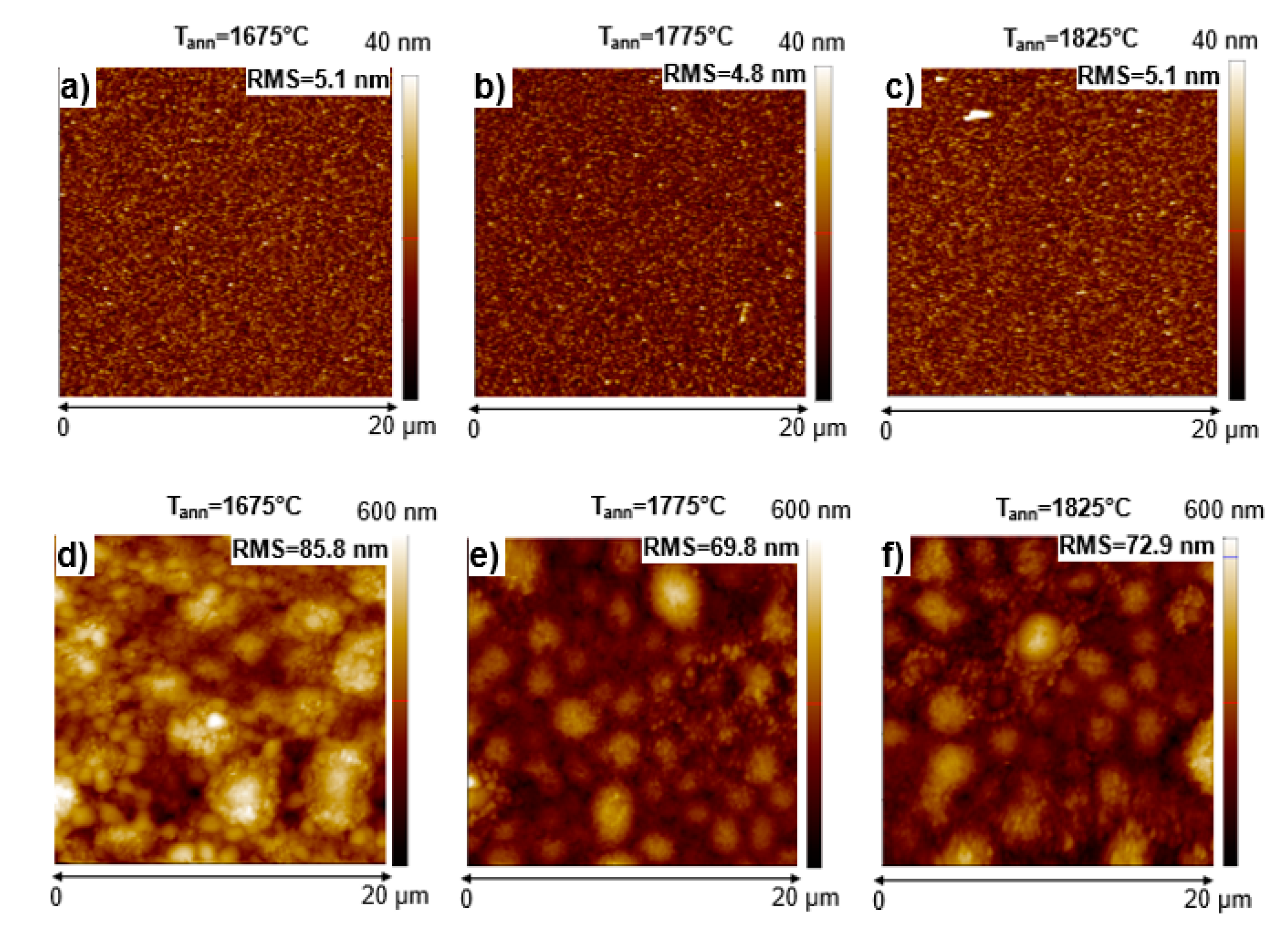
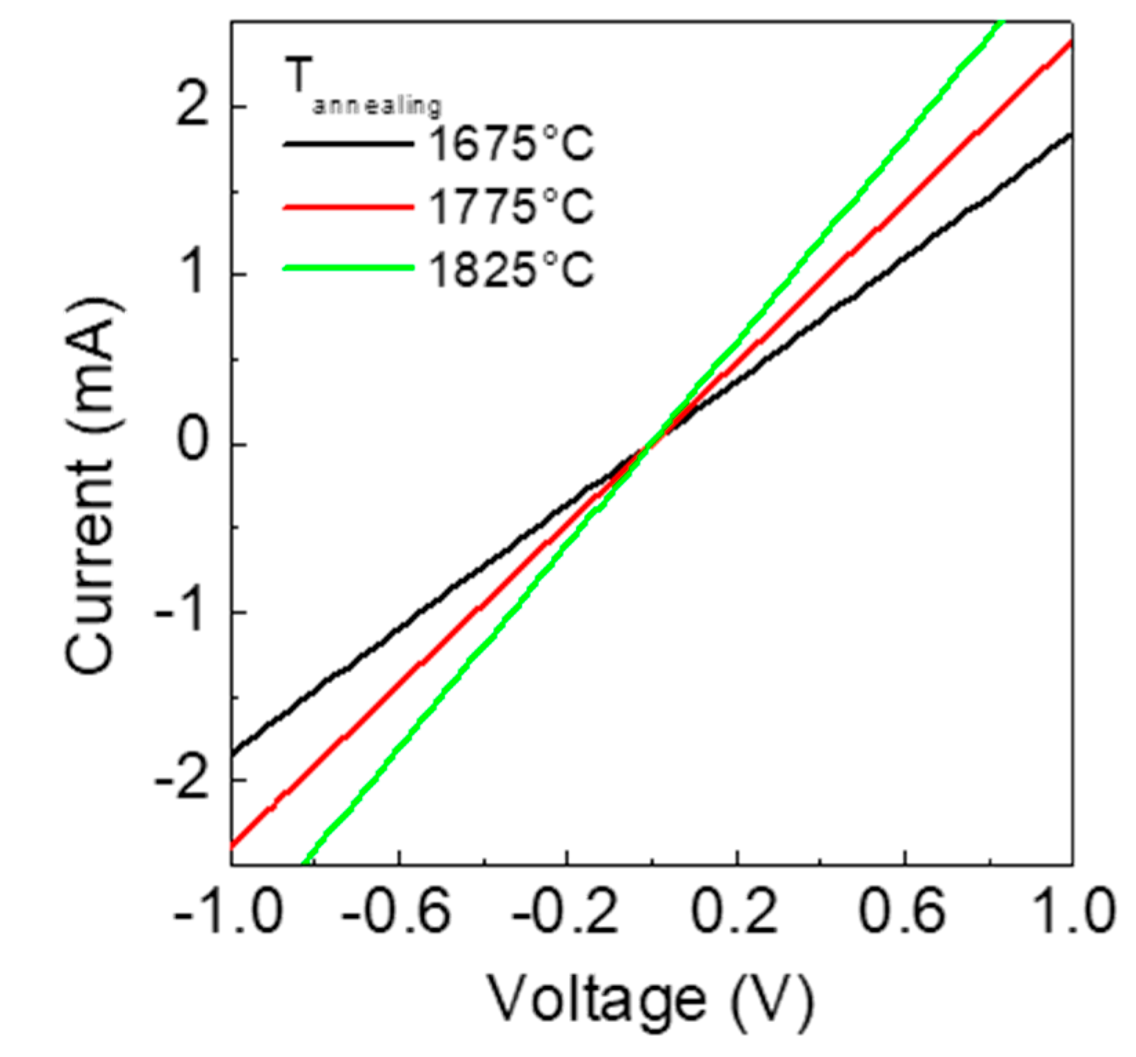
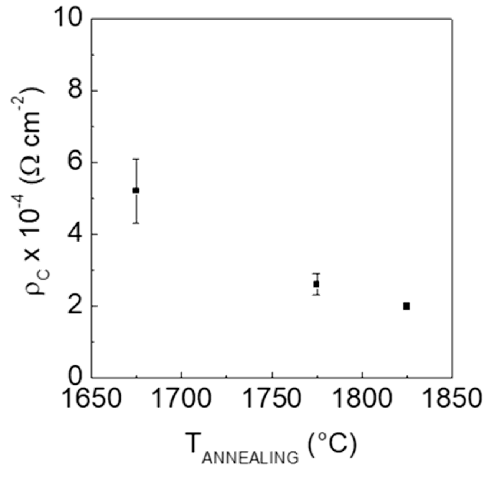
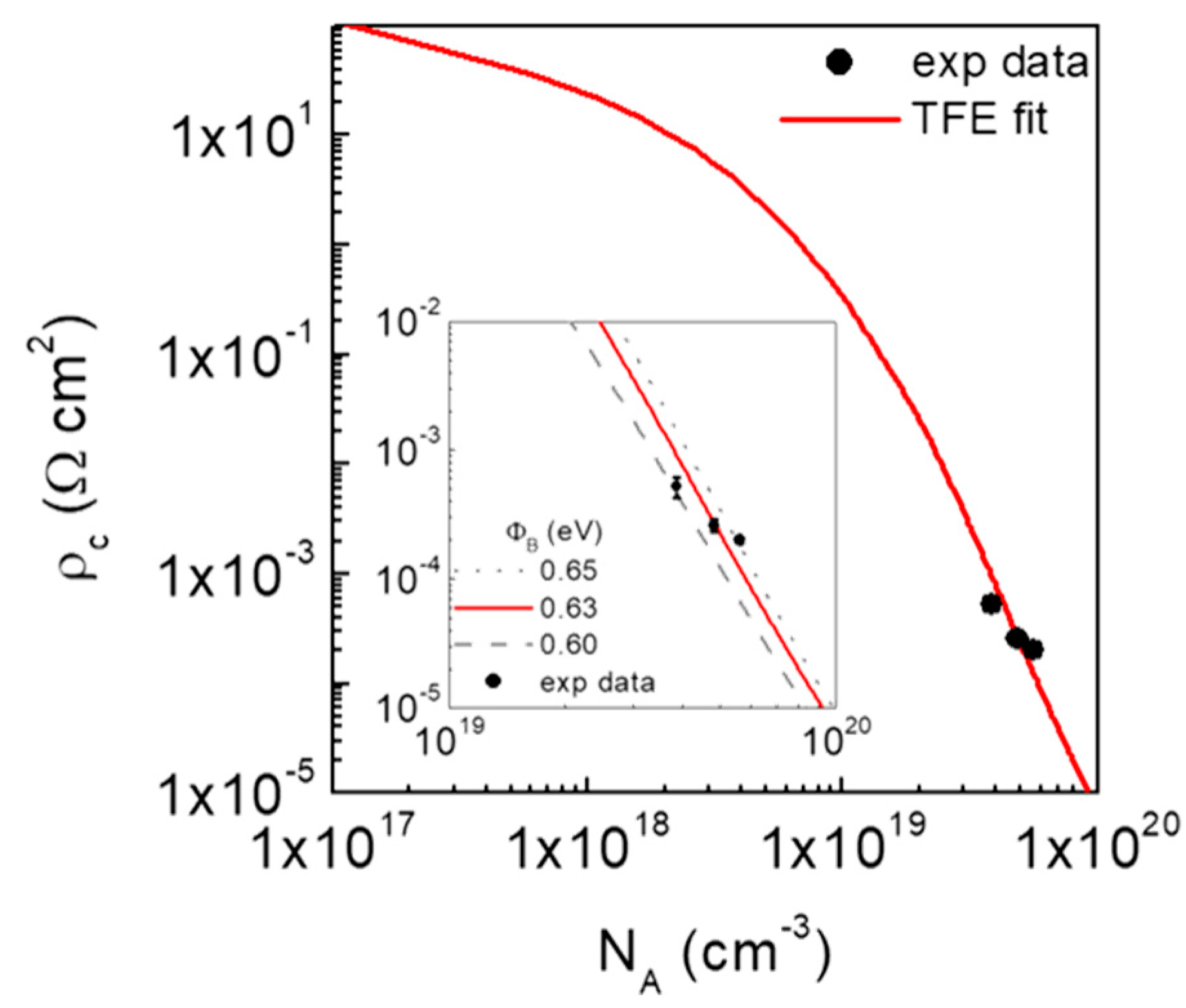
3. Results and Discussion

Firstly, Van der Paw and Hall Effect measurements were carried out to determine the electrical properties of the Al-implanted 4H-SiC layers annealed at different temperatures. In particular, I–V measurements on Van der Paw structures allowed to determine the sheet resistance of p-type 4H-SiC. Then, assuming a uniform doping over the entire implanted thickness of 300 nm, the resistivity of the implanted layer (Ω cm) could be extracted. The activation energy EA of the Al-implanted dopant was determined from an Arrhenius plot of the 4H-SiC sheet resistance. The values of EA in the range of 99–110 meV are in agreement with typical literature values reported for these high acceptor concentrations, as well as with the theoretical relation between EA and NA in 4H-SiC [12,32].
Then, using this parameter, the temperature dependence of the hole concentration extracted by Hall Effect measurements could be fitted using the neutrality equation [31], determining the active acceptor concentration (NA), the concentration of compensating centers (ND) associated to residual implant defects after annealing, the percentage of an electrically active Al dopant, and the compensation ratio (ND/NA). Table I summarizes the main results of these electrical analyses carried out on the p-type-implanted 4H-SiC layers, subjected to different post-implantation annealing treatments (1675 °C, 1775 °C, and 1825 °C).
Then, Ti/Al/Ni contacts were deposited on the implanted layers. These contacts were characterized from the morphological and electrical point of view. Figure 1a–c shows the AFM images of as deposited Ti/Al/Ni contacts on p-type-implanted 4H-SiC samples, subjected to three different post-implantation annealing temperatures. Independent of the annealing process of the underlying material, the contacts have a similar morphology, with root mean square (RMS) roughness values in the range of 4.8–5.1 nm. Figure 1d–f shows the morphologies of the same Ti/Al/Ni contacts after annealing in Ar at 950 °C. Evidently, the annealing process resulted in an increase in the RMS of the contacts, due to the thermal reaction of the layer and to the presence of some metallic hillocks on the sample surface. In particular, the RMS values were 85.8 nm at 1675 °C, 69.8 nm at 1775 °C, and 72.9 nm at 1825 °C.
In fact, it has been previously reported that thermal annealing of Ti/Al/Ni layers on 4H-SiC, results in an intermixing of the metal layer, with the formation of new phases (mainly Al3Ni2), which are characterized by a high surface roughness [25].
The electrical characterization of the contacts has been performed by I–V measurements on the fabricated TLM structures. Figure 2 shows the comparison of I–V curves acquired between adjacent contacts of the TLM structure (placed at a distance of 20 µm), for the three samples. As can be seen, linear characteristics are obtained in all three cases. Moreover, a gradual increase in the current is observed with the increase of the post-implantation annealing temperature from 1675 °C to 1825 °C.
From the slope of the I–V curves acquired in the three samples at different TLM pad distances, it was possible to extract the total resistance RTOT. Figure 3 reports the plots of the total resistance RTOT as a function of the distance d between the TLM pads. The different slope of RTOT in the three samples is due to the different sheet resistance of the 4H-SiC-implanted layers. In particular, the linear fits of the data gave the following values of sheet resistance of the p-type-implanted 4H-SiC: 12.4 kΩ/sq (Tann = 1675 °C), 9.8 kΩ/sq (Tann = 1775 °C), and 8.0 kΩ/sq (Tann = 1825 °C). Such values are in agreement with those extracted by Hall measurements (see Table 1), considering the thickness of the implanted layer (300 nm) [12]. Moreover, the resistivity values are consistent with the literature data obtained for 4H-SiC layers with a similar acceptor concentration (3–6 × 1019 cm−3) [10,14,17,24,25].
The TLM analysis allowed determining the following values of the specific contact resistance: 5.2 × 10⁻⁴ Ω cm2 at Tann = 1675 °C, 2.6 × 10⁻⁴ Ω cm2 at Tann = 1775 °C and 2.0 × 10⁻⁴ Ω cm2 at Tann = 1825 °C.
As summarized in Figure 4, the values of ρc decrease with the increase of the post-implantation annealing temperature. This result is correlated with the improved Al activation.
To complete the electrical characterization of the Ohmic contacts, the current transport mechanism at the metal/semiconductor interface has been studied. Generally, for intermediate values of the doping concentration (1017 < NA < 1019 cm−3), current transport across the metal/semiconductor barrier is ruled by the Thermionic Field Emission (TFE) mechanism [33,34]. More specifically, the dominant current injection mechanism at the interface with 4H-SiC can be established by comparing the characteristic energy E00 with the thermal energy kT (where k is the Boltzmann constant and T is the temperature). The characteristic energy E00 is defined as:
E 00 = q h 4 π N A m * ε
where h is the Planck constant, ε is the dielectric constant of 4H-SiC, m* is the tunneling effective mass, and NA is the doping concentration. In particular, for E00kT, TFE represents the main transport mechanism. For the NA values in our samples (Table 1), the calculated E00 was in the range of 39–47 meV, which is comparable with kT of our measurement range. Hence, the temperature dependence of ρc was described by the TFE expression:
ρ c T F E = k E 00 cosh ( E 00 / k T ) coth ( E 00 / k T ) A * T q π q ( Φ B V p ) e x p [ q ( Φ B V p ) E 00 coth ( E 00 / k T ) + q V p k T ]
where ΦB is the metal/p-SiC barrier height, k is the Boltzmann constant, A* is the Richardson constant, and Vp is the energy difference between the valence-band edge and the Fermi level.
Figure 5 reports the experimental ρc values as a function of NA for our three samples and the best fit of these data with Equation (2) using ΦB as the only fitting parameter. This plot illustrates the dependence of the ρc-TFE function on the acceptor concentration in a wide concentration range, from 1017 to 1020 cm−3. For a better visualization, a plot of the data in a narrower range of NA values (1019–1020 cm−3) is also shown in the inset of Figure 5, together with the calculated ρc vs NA curves for values of ΦB = 0.60 eV, ΦB = 0.63 eV, and ΦB = 0.65 eV. This comparison confirms that ΦB = 0.63 eV is the barrier height value that better accounts for the experimental dependence of the contact resistance.
Other literature works described the carrier transport for Ti/Al-based contacts with the TFE model [17,19,21,24,25]. From the fit of the specific contact resistance, different values of barrier height have been obtained (see Table 2). Clearly, the value of the barrier height depends on the different experimental parameters, such as the doping, the deposition technique, the metal thickness, and the annealing conditions [35]. From Table 2, it is interesting to note that Frazzetto et al. [17] obtained a lower ΦB of 0.46 eV using Ti/Al contacts. The lowering of the barrier has been attributed to the formation of the ternary phase Ti3SiC2 [19,20,21]. A slightly higher barrier height of 0.56 eV has been reported by Vivona et al. [25] for Ti/Al/Ni contacts (similar to our samples). In this case, an interfacial TiC layer is observed at the metal/4H-SiC interface and it has been indicated as responsible for the Ohmic behavior. An even higher barrier (0.69 eV) has been measured using Ti/Al/W [24]. In addition, barrier height values of 0.71 eV [21] or 0.82 eV [36] have been obtained using a Ti/Al scheme with different metal thickness and different annealing conditions. Hence, it is clear how the different microstructure changes occurring at the interface after thermal treatment play a key role in the value of the barrier height.

4. Conclusions

In conclusion, this work discussed the electrical behavior of Ohmic contacts on p-type Al-implanted 4H-SiC layers activated under different post-implantation annealings (1675 °C, 1175 °C, and 1825 °C). Ti/Al/Ni Ohmic contacts formed with a rapid annealing at 950 °C, exhibited values of the specific contact resistance in the 10−4 Ω cm2 range, which decreased with the increase of the post-implantation annealing temperature. The dependence of ρc on the active acceptor concentration is ruled by the thermionic field emission model, with a barrier height of 0.63 eV. These results can be useful to set the optimal processing conditions for Ohmic contacts on p-type regions in 4H-SiC devices.

Author Contributions

The authors gave the following contribute to this work: electrical measurements and data analyses M.S., G.G. and D.C.; vdP and TLM structures fabrication S.D.F.; definition of experimental doping parameters A.S.; management of the funded project A.A.M; interpretation of electrical results F.G.; scientific coordination, data analysis, manuscript writing and review F.R.

Funding

This research was funded by the European ECSEL JU project REACTION (grant agreement no. 783158).

Acknowledgments

The authors would like to acknowledge Raffaella Lo Nigro and Patrick Fiorenza for the fruitful discussions on structural and nanoscale characterizations. Moreover, the colleagues of STMicroelectronics are acknowledged for technical support with ion-implantation and high temperature annealing of 4H-SiC samples.

Conflicts of Interest

The authors declare no conflict of interest.

References

  1. Kimoto, T.; Cooper, J. Fundamentals of Silicon Carbide Technology: Growth, Characterization, Devices and Applications; John Wiley & Sons: Singapore, 2014. [Google Scholar]
  2. Roccaforte, F.; Fiorenza, P.; Greco, G.; Lo Nigro, R.; Giannazzo, F.; Patti, A.; Saggio, M. Challenges for energy efficient wide band gap semiconductor power devices. Phys. Status Solidi A 2014, 211, 2063–2071. [Google Scholar] [CrossRef]
  3. Roccaforte, F.; Fiorenza, P.; Greco, G.; Lo Nigro, R.; Giannazzo, F.; Iucolano, F.; Saggio, M. Emerging trends in wide band gap semiconductors (SiC and GaN) technology for power devices. Microelectr. Eng. 2018, 187–188, 66–77. [Google Scholar] [CrossRef]
  4. Wong-Leung, J.; Janson, M.S.; Kuznetsov, A.; Svensson, B.G.; Linnarsson, M.K.; Hallén, A.; Jagadish, C.; Cockayne, D.J.H. Ion Implantation in 4H-SiC. Nucl. Istr. Meth. B 2008, 266, 1367–1372. [Google Scholar] [CrossRef]
  5. Negoro, Y.; Kimoto, T.; Matsunami, H.; Schmid, F.; Pensl, G. Electrical activation of high-concentration aluminum implanted in 4H-SiC. J. Appl. Phys. 2004, 96, 4916–4922. [Google Scholar] [CrossRef] [Green Version]
  6. Fujihara, H.; Suda, J.; Kimoto, T. Electrical properties of n- and p-type 4H-SiC formed by ion implantation into high-purity semi-insulating substrates. Jpn. J. Appl. Phys. 2017, 56, 070306. [Google Scholar] [CrossRef]
  7. Nipoti, R.; Ayedh, H.M.; Svensson, B.G. Defects related to electrical doping of 4H-SiC by ion implantation. Mater. Sci. Semicond. Proc. 2018, 78, 13–21. [Google Scholar] [CrossRef]
  8. Roccaforte, F.; Frazzetto, A.; Greco, G.; Giannazzo, F.; Fiorenza, P.; Lo Nigro, R.; Saggio, M.; Leszczynski, M.; Prystawko, P.; Raineri, V. Critical issues for interfaces to p-type SiC and GaN in power devices. Appl. Surf. Sci. 2012, 258, 8324–8333. [Google Scholar] [CrossRef]
  9. Pernot, J.; Contreras, S.; Camassel, J. Electrical transport properties of aluminium-implanted 4H-SiC. J. Appl. Phys. 2005, 98, 023706. [Google Scholar] [CrossRef]
  10. Rambach, M.; Bauer, A.J.; Ryssel, H. Electrical and topographical characterization of aluminium implanted layers in 4H silicon carbide. Phys. Stat. Sol. B 2008, 245, 1315–1326. [Google Scholar] [CrossRef]
  11. Rambach, M.; Bauer, A.J.; Ryssel, H. High Temperature Implantation of Aluminum in 4H Silicon Carbide. Mater. Sci. Forum Vols 2007, 556–557, 587–590. [Google Scholar] [CrossRef]
  12. Spera, M.; Corso, D.; Di Franco, S.; Greco, G.; Severino, A.; Fiorenza, P.; Giannazzo, F.; Roccaforte, F. Effect of high temperature annealing (T > 1650 °C) on the morphological and electrical properties of p-type implanted 4H-SiC layers. Mater. Sci. Semicond. Proc. 2019, 93, 274–279. [Google Scholar] [CrossRef]
  13. Roccaforte, F.; La Via, F.; Raineri, V. Ohmic contacts to SiC. Int. J. High Speed Electr. Syst. 2005, 15, 781–820. [Google Scholar] [CrossRef]
  14. Vivona, M.; Greco, G.; Giannazzo, F.; Lo Nigro, R.; Rascunà, S.; Saggio, M.; Roccaforte, F. Thermal stability of the current transport mechanisms in Ni-based Ohmic contacts on n-and p-implanted 4H-SiC. Semicond. Sci. Technol. 2014, 29, 075018. [Google Scholar] [CrossRef]
  15. Crofton, J.; Mohney, S.E.; Williams, J.R.; Isaacs-Smith, T. Finding the optimum Al–Ti alloy composition for use as an ohmic contact to p-type SiC. Solid State Electron. 2002, 46, 109. [Google Scholar] [CrossRef]
  16. Johnson, B.J.; Capano, M.A. The effect of titanium on Al–Ti contacts to p-type 4H-SiC. Solid State Electron. 2003, 47, 1437. [Google Scholar] [CrossRef]
  17. Frazzetto, A.; Giannazzo, F.; Lo Nigro, R.; Raineri, V.; Roccaforte, F. Limiting mechanism of inversion channel mobility in Al-implanted lateral 4H-SiC metal-oxide semiconductor field-effect transistors. J. Phys. D Appl. Phys. 2011, 44, 255302. [Google Scholar] [CrossRef]
  18. Wang, Z.; Liu, W.; Wang, C. Recent progress in Ohmic contacts to silicon carbide for high-temperature applications. J. Electron. Mater. 2016, 45, 267. [Google Scholar] [CrossRef]
  19. Fisher, C.A.; Jennings, M.R.; Sharma, Y.K.; Sanchez-Fuentes, A.; Walker, D.; Gammon, P.M.; Pérez-Tomás, A.; Thomas, S.M.; Burrows, S.E.; Mawby, P.A. On the Schottky Barrier Height Lowering Effect of Ti3SiC2 in Ohmic Contacts to P-Type 4H-SiC. Int. J. Fund. Phys. Sci. 2014, 4, 95–100. [Google Scholar] [CrossRef]
  20. Nakatsuka, O.; Takei, T.; Koide, Y.; Murakami, M. Low resistance TiAl ohmic contacts with multi-layered structure for p-type 4H-SiC. Mater. Trans. 2002, 43, 1684. [Google Scholar] [CrossRef]
  21. Abi-Tannous, T.; Souedain, M.; Ferro, G.; Lazar, M.; Raynaud, C.; Toury, B.; Beafourt, M.F.; Barbot, J.F.; Dezellus, O.; Planson, D. A Study on the Temperature of Ohmic Contact to p-Type SiC Based on Ti3SiC2Phase. IEEE Trans. Electron. Dev. 2016, 63, 2462. [Google Scholar] [CrossRef]
  22. Tamaso, H.; Yamada, S.; Kitabayashi, H.; Horii, T. Ti/Al/Si Ohmic Contacts for Both n-Type and p-Type 4H-SiC. Mater. Sci. Forum 2014, 669, 778–780. [Google Scholar] [CrossRef]
  23. Jennings, M.R.; Fisher, C.A.; Walker, D.; Sanchez, A.; Perez-Tomas, A.; Hamilton, D.P.; Gammon, P.M.; Burrows, S.E.; Thomas, S.M.; Sharma, Y.; et al. On the Ti3SiC2 metallic phase formation for robust p-type 4H-SiC ohmic contacts. Mater. Sci. Forum 2014, 693, 778–780. [Google Scholar]
  24. Vivona, M.; Greco, G.; Lo Nigro, R.; Bongiorno, C.; Roccaforte, F. Ti/Al/W Ohmic contacts to p-type implanted 4H-SiC. J. Appl. Phys. 2015, 118, 035705. [Google Scholar] [CrossRef]
  25. Vivona, M.; Greco, G.; Bongiorno, C.; Lo Nigro, R.; Scalese, S.; Roccaforte, F. Electrical and structural properties of surfaces and interfaces in Ti/Al/Ni Ohmic contacts to p-type implanted 4H-SiC. Appl. Surf. Sci. 2017, 420, 331–335. [Google Scholar] [CrossRef]
  26. Konishi, R.; Yasukochi, R.; Nakatsuka, O.; Koide, Y.; Moriyama, M.; Murakami, M. Development of Ni/Al and Ni/Ti/Al ohmic contact materials for p-type 4H-SiC. Mater. Sci. Eng. 2003, B98, 286. [Google Scholar] [CrossRef]
  27. Yu, H.; Zhang, X.; Shen, H.; Tang, Y.; Bai, Y.; Wu, Y.; Liu, K.; Liu, X. Thermal stability of Ni/Ti/Al ohmic contacts to p-type 4H-SiC. J. Appl. Phys. 2015, 117, 025703. [Google Scholar] [CrossRef]
  28. Jennings, M.R.; Pérez-Tomás, A.; Davies, M.; Walker, D.; Zhu, L.; Losee, P.; Huang, W.; Balachandran, S.; Guy, O.J.; Covington, J.A.; et al. Analysis of Al/Ti, Al/Ni multiple and triple layer contacts to p-type 4H-SiC. Solid State Electron. 2007, 51, 797. [Google Scholar] [CrossRef]
  29. Vang, H.; Lazar, M.; Brosselard, P.; Raynaud, C.; Cremillieu, P.; Leclercq, J.-L.; Bluet, J.-M.; Scharnholz, S.; Planson, D. Ni–Al ohmic contact to p-type 4H-SiC. Superlattices Microstruct. 2006, 40, 626. [Google Scholar] [CrossRef]
  30. Vassilevski, K.V.; Wright, N.G.; Nikitina, I.P.; Horsfall, A.B.; O’Neill, A.G.; Uren, M.J.; Hilton, K.P.; Masterton, A.G.; Hydes, A.J.; Johnson, C.M. Protection of selectively implanted and patterned silicon carbide surfaces with graphite capping layer during post-implantation annealing. Semicond. Sci. Technol. 2005, 20, 271–278. [Google Scholar] [CrossRef]
  31. Schroder, D.K. Semiconductor Material and Device Characterization, 3rd ed.; John Wiley & Sons Inc.: Hoboken, NJ, USA, 2006. [Google Scholar]
  32. Pearson, G.L.; Bardeen, J. Electrical properties of pure silicon and silicon alloys containing boron and phosphorus. Phys. Rev. 1949, 75, 865. [Google Scholar] [CrossRef]
  33. Greco, G.; Iucolano, F.; Roccaforte, F. Ohmic contacts to Gallium Nitride materials. Appl. Surf. Sci. 2016, 383, 324–345. [Google Scholar] [CrossRef]
  34. Padovani, F.A.; Stratton, R. Field and thermionic-field emission in Schottky barriers. Solid State Electron. 1966, 9, 695–707. [Google Scholar] [CrossRef]
  35. Roccaforte, F.; Vivona, M.; Greco, G.; Lo Nigro, R.; Giannazzo, F.; Rascunà, S.; Saggio, M. Metal/semiconductor contacts to Silicon Carbide: Physics and technology. Mater. Sci. Forum 2017, 924, 339–344. [Google Scholar] [CrossRef]
  36. Scorzoni, A.; Moscatelli, F.; Poggi, A.; Cardinali, G.C.; Nipoti, R. Contact resistivity and barrier height of Al/Ti ohmic contacts on p-type ion implanted 4H-and 6H-SiC. Mater. Sci. Forum 2004, 457–460, 881–884. [Google Scholar] [CrossRef]
Figure 1. AFM images of the as deposited (ac) and annealed (950 °C) Ti/Al/Ni contacts (df)) on Al-implanted silicon carbide (4H-SiC) samples, activated at three different post-implantation annealing temperatures (1675 °C, 1775 °C, and 1825 °C).
Materials 12 03468 g001
Figure 2. I–V curves of Ti/Al/Ni Ohmic contacts (formed at 950 °C), acquired between adjacent TLM pads at a distance of 20 µm. The Al-implanted silicon carbide (4H-SiC) samples were activated at three different post-implantation annealing temperatures (1675 °C, 1775 °C, and 1825 °C).
Materials 12 03468 g002
Figure 3. Plots of the total resistance RTOT as a function of the TLM pad distance d, used for the extraction of the specific contact resistance, on Al-implanted 4H-SiC samples subjected to post-implantation annealing at Tann = 1675 °C, Tann = 1775 °C, and Tann = 1825 °C.
Materials 12 03468 g003
Figure 4. Specific contact resistance of Ti/Al/Ni contacts on p-type-implanted 4H-SiC layers as a function of the post-implantation annealing temperature.
Materials 12 03468 g004
Figure 5. Specific contact resistance ρc of Ti/Al/Ni Ohmic contacts as a function of the acceptor concentration NA in p-type-implanted 4H-SiC. The continuous line is the fit of the experimental data obtained using the TFE model with a barrier height of 0.63 eV. Inset: simulated curves for values of ΦB = 0.60 eV, ΦB = 0.63 eV, and ΦB = 0.65 eV.
Materials 12 03468 g005
Table 1. Summary of the main electrical results obtained on p-type-implanted 4H-SiC layers, subjected to different post-implantation annealing at different temperatures (1675 °C, 1775 °C, and 1825 °C).
Annealing TemperatureMaterial Resistivity (Ω cm)EA (meV)NA (cm−3)ND (cm−3)Al ActivationCompensation Ratio ND/NA
1675 °C0.361103.87 × 10193.66 × 101839%9.4%
1775 °C0.291054.84 × 10193.49 × 101848%7.2%
1825 °C0.22995.64 × 10193.48 × 101856%6.2%
Table 2. Survey of literature results on Ti/Al-based Ohmic contacts to p-type 4H-SiC, formed under different annealing conditions. The reported barrier height values have been determined by TFE model.
Metal SchemeAnnealing ConditionsΦB (eV)Ref.
Ti(100 nm)/Al(300 nm)950 °C (1 min, Ar)0.46[17]
Ti(30 nm)/Al(70 nm)1000 °C (1 min, Ar)0.71[21]
Ti(70 nm)/Al(200 nm)/Ni(50 nm)950 °C (1 min, Ar)0.56[25]
Ti(70 nm)/Al(200 nm)/W(50 nm)1100 °C (1 min, Ar)0.69[24]
Ti(30 nm)/Al(100 nm)/NiV(25 nm)1000 °C (2 min, Ar)0.43[19]
Ti(70 nm)/Al(200 nm)/Ni(50 nm)950 °C (1 min, Ar)0.63This work

