ZnO-Controlled Growth of Monolayer WS2 through Chemical Vapor Deposition


1
College of Materials & Environmental Engineering, Hangzhou Dianzi University, Hangzhou 310018, China
2
Tsinghua-Berkeley Shenzhen Institute (TBSI), Tsinghua University, Shenzhen 518055, China
*
Authors to whom correspondence should be addressed.
Materials 2019, 12(12), 1883; https://doi.org/10.3390/ma12121883
Submission received: 16 May 2019
/
Revised: 5 June 2019
/
Accepted: 6 June 2019
/
Published: 12 June 2019
(This article belongs to the Special Issue Graphene and Other 2D Layered Nanomaterials and Hybrid Structures: Synthesis, Properties and Applications)
Abstract
:Monolayer tungsten disulfide (2D WS2) films have attracted tremendous interest due to their unique electronic and optoelectronic properties. However, the controlled growth of monolayer WS2 is still challenging. In this paper, we report a novel method to grow WS2 through chemical vapor deposition (CVD) with ZnO crystalline whisker as a growth promoter, where partially evaporated WS2 reacts with ZnO to form ZnWO4 by-product. As a result, a depletion region of W atoms and S-rich region is formed which is favorable for subsequent monolayer growth of WS2, selectively positioned on the silicon oxide substrate after the CVD growth.
1. Introduction
Two dimensional (2D) materials such as graphene, hexagonal boron nitride, and transition metal dichalcogenides have attracted tremendous attention from scientists in materials science, physics, and chemistry for their monolayer structure and properties [1,2,3]. Monolayer WS2 is one of the typical 2D materials with a suitable direct band gap ca 2.0 eV showing potential applications in sensors, electronics, and optoelectronics [4,5,6,7,8]. Recently, many methods have been used to prepare monolayer WS2, such as mechanical exfoliation, as well as wet chemical and hydrothermal synthesis [9,10,11,12]. Chemical vapor deposition (CVD) is considered the most suitable method for the preparation of monolayer WS2 used for thin film devices [13]. In the CVD method, tungsten oxide and sulfide powders are commonly used as precursors, which evaporate at high temperature and react to form WS2. Large-scale monolayer WS2 has been reported to be grown on an Au substrate [14]. To integrate with silicon integrated circuit technology, the growth of WS2 on a silicon dioxide (SiO2) substrate is preferred [15,16]. Many works have focused on the deposition of the monolayer WS2 on the SiO2 substrate by CVD [17,18,19]. However, the deposition has poor reproducibility caused by the growth conditions [20]. In addition, the 2D WS2 obtained is combined with monolayer and multilayers [19,21,22]. The selective growth and the positioning of monolayer WS2 are not under control. Besides the controlled growth, the mechanism of the monolayer WS2 formation is still under discussion. Fan et al. provided an understanding of the dislocation-driven growth mechanism of 2D nanostructures in their work [23]. Cain et al. found that transition metal dichalcogenide monolayer growth proceeds from nominal lyoxi-chalcogenide nanoparticles which act as heterogeneous nucleation sites for monolayer growth [24]. The reaction of tungsten oxide in sulfur vapor suggests that the growth of WS2 is thermodynamically correlated with the sulfur concentration. We hypothesized that if the sulfur concentration could be controlled, it would be possible to deposit WS2 with the desired thickness.
Herein, we report a novel method to selectively grow monolayer WS2 on SiO2 substrate. ZnO crystal whisker is used to mediate the spacial distribution of sulfur concentration. We show that monolayer WS2 symmetrically distributes on both sides of the ZnO crystal whisker. By constructing a concentration distribution model, the monolayer growth mechanism can be discussed.
2. Materials and Methods
2.1. WS2 Monolayer Preparation
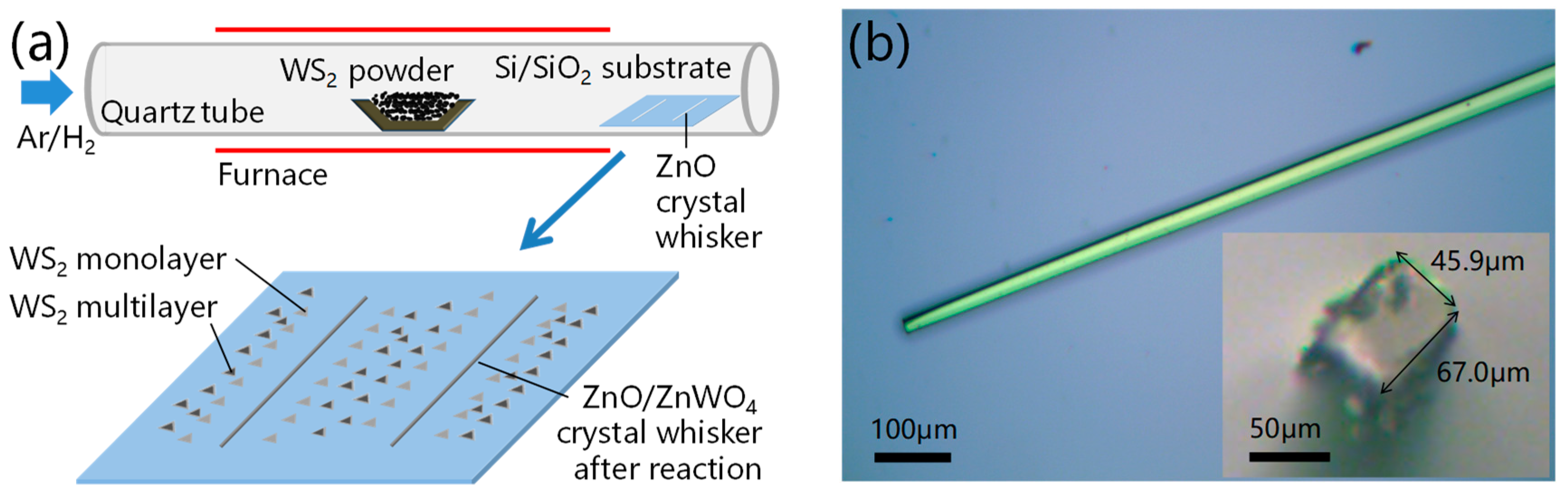
Figure 1a shows a schematic diagram of the home-built CVD system. WS2 powders (2.0 g, purity 99.5%, Aladdin, Shanghai, China) used as precursor were loaded into a quartz boat and put at the center of a quartz tube (1 inch in diameter). Silicon wafer with a 300 nm thick oxide layer used as substrate (SiO2/Si) was placed at the low temperature region of the quartz tube downstream of the carrier gas. Ar/H2 (5% H2) was used as carrier gas. ZnO crystal whiskers (1.5 cm in length) were obtained by thermal evaporation of ZnO powders according to the reference and transferred onto the substrate [25]. Figure 1b shows a typical ZnO crystal whisker with a size of 67.0 μm × 45.9 μm × 1500 μm.
For the growth of the WS2, the carrier gas with 35 sccm was introduced into the CVD system, which was evacuated to 70 torr. Then the furnace was heated from room-temperature to 1000 °C in 40 min and kept for 1 h. After that, the furnace was cooled down from 1000 °C to room-temperature under carrier gas flow.
2.2. Characterizations
Optical and photoluminescence (PL) imagings were carried out on a Jiangnan MV3000 digital microscope (Nanjing Jiangnan Novel Optics Co., Ltd.; Nanjing, China). Scanning electron microscopy (SEM) was conducted on a field emission scanning electron microscope (FESEM, ULTRA 55, Zeiss, Heidenheim, Germany). Photoluminescence (PL) and Raman spectra were acquired on a home-built Raman system, consisting of an inverted microscope (Ti eclipse, Nikon, Tokyo, Japan), a Raman spectrometer (iHR320, Horiba, Kyoto, Japan) with CCD detector (Syncerity, Horiba, Kyoyo, Japan) and a semiconductor laser at 532 nm (Uniklasers, Glasgow, UK). All measurements were performed at room temperature.
3. Results and Discussion
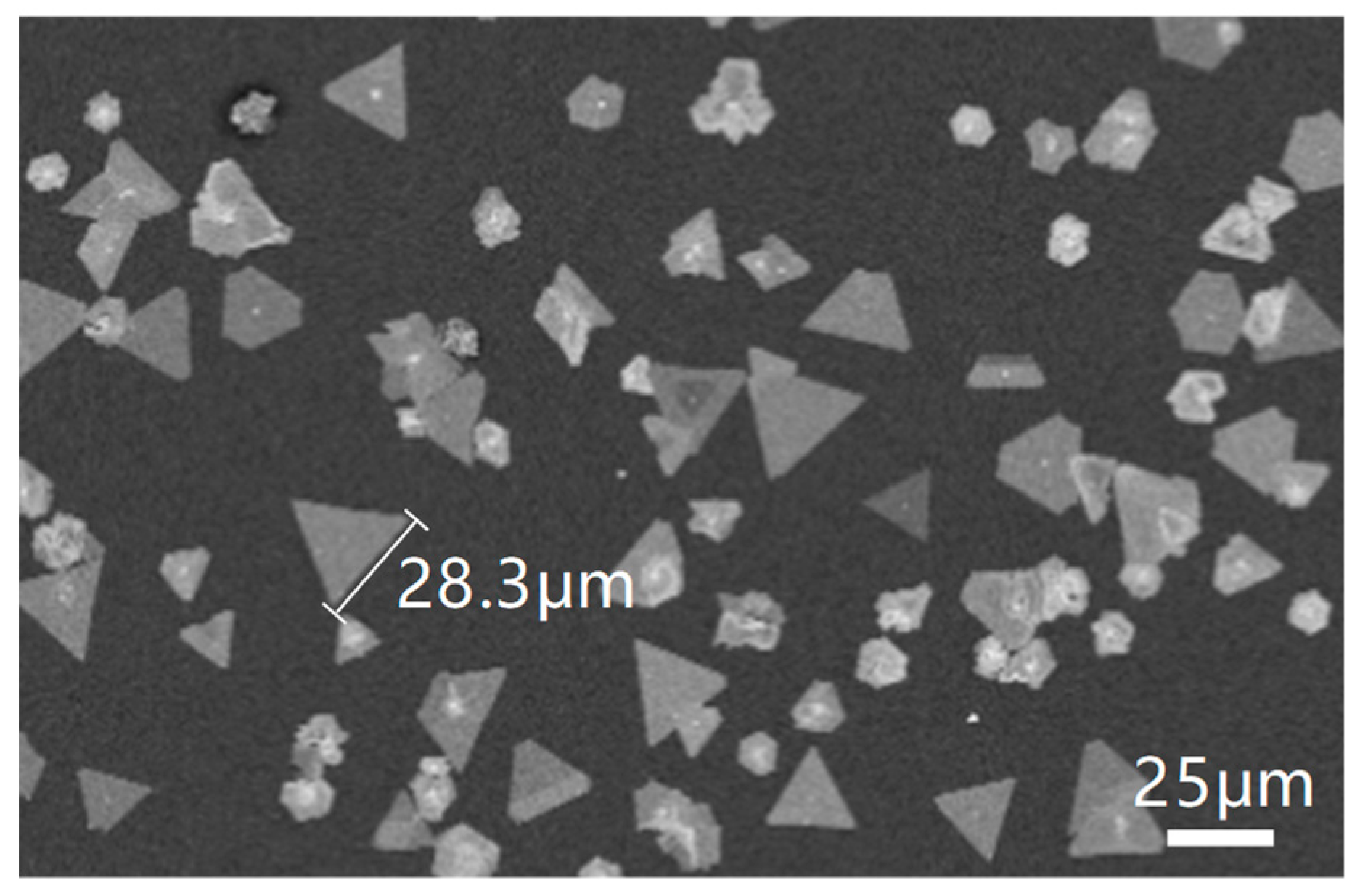
Figure 2 shows the SEM image of the WS2 grown on the SiO2/Si substrate. We can see the separated WS2 domains of a triangular and hexagonal shape. The maximum size of the domain is up to 28.3 μm.
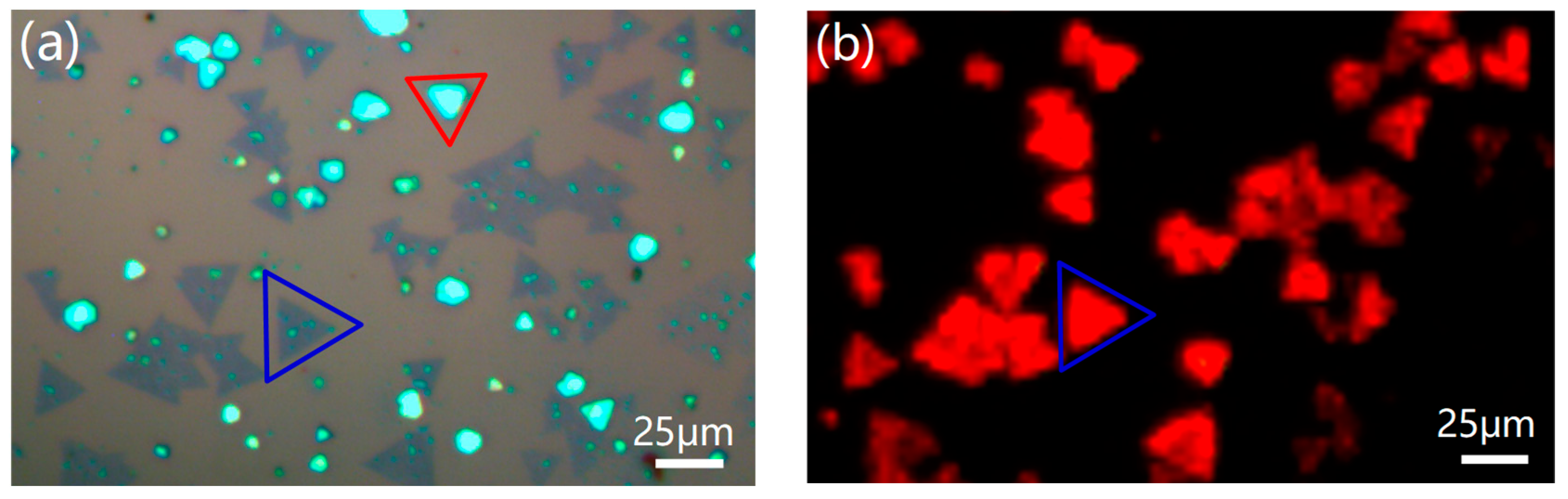
Figure 3a shows the optical microscopy image of the sample. The dark region marked with a blue triangle is monolayer WS2 while the bright region marked with a red triangle is due to multilayer WS2. The uniform color contrast of the monolayer indicates the thickness uniformity of the WS2 monolayer. Figure 3b shows the PL image corresponding to the sample in Figure 3a taken at the same location. The excitation wavelength was 485 nm. The monolayer WS2 displays super-bright red light emitting under irradiation. The patterns with the red color in Figure 3b remain as features of the monolayer WS2 domains in Figure 3a. However, the PL emission of multilayer WS2 is not strong enough to be detected by photoluminescence microscopy. The difference of the PL behavior between the monolayer and multilayer lies in the different electrical structures. Monolayer WS2 is a direct band gap, while multilayer is an indirect band gap [26]. The fluorescence quantum efficiency of the direct band gap semiconductor is much higher than that of the indirect [27,28]. Therefore, we only observe the PL image in the monolayer WS2.
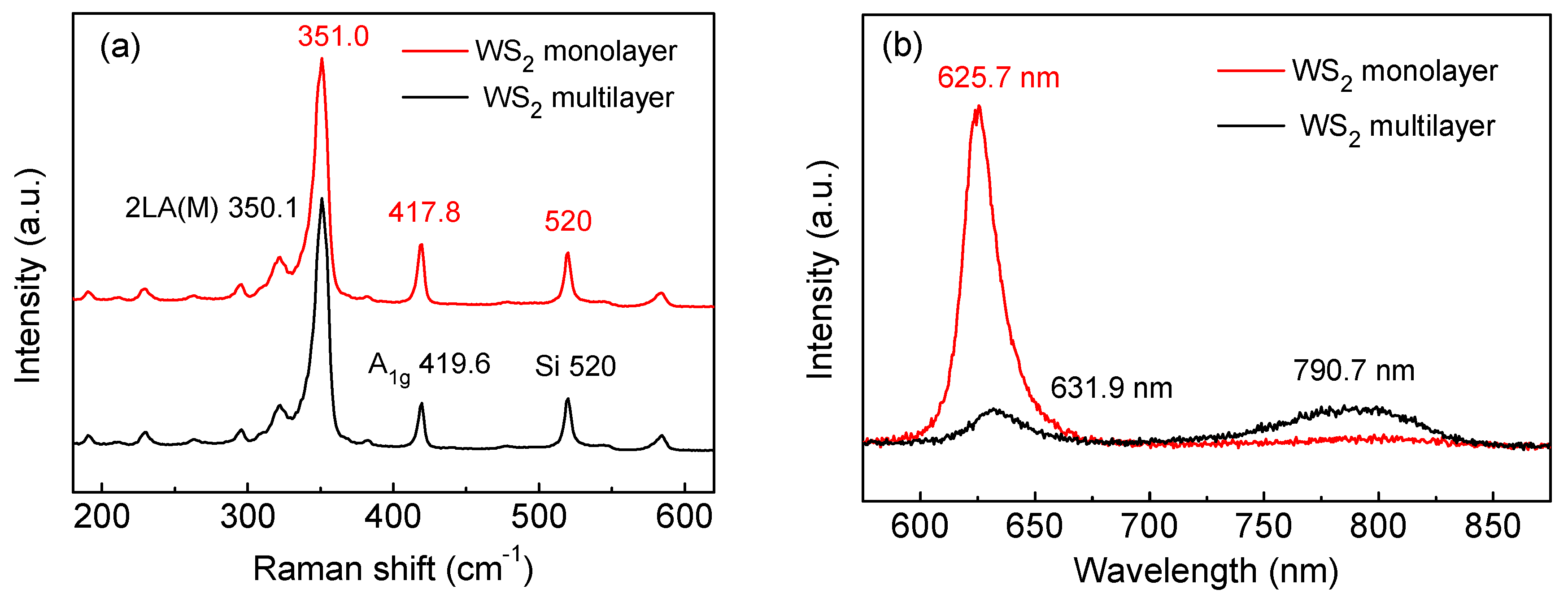
Figure 4 shows the Raman and PL spectra of the WS2 monolayer (red line) and multilayer (black line). Raman spectroscopy was used to identify the number of two dimensional material layers. Raman peaks at 351.1 cm−1, 417.2 cm−1 are the fingerprint peaks of monolayer WS2, which are due to the second-order longitudinal acoustic mode (2LA(M)), and out-of-plane vibration mode (A1g), respectively [29]. With the increase of the number of layers, the 2LA(M) peak red shifts and the A1g peak blueshifts. The 2LA(M) and A1g peaks are observed in Figure 4a. For the domain marked with a blue triangle in Figure 3a, Raman peaks located at 351.0 cm−1 (2LA(M)) and 417.8 cm−1 (A1g) were observed, indicating the thickness of the domain is monolayer. For the domain marked with a red triangle in Figure 3a, the 2LA(M) peak redshifted to 350 cm−1 and A1g peak blueshifted to 419.6 cm−1, indicating the thickness of the domain is multilayer [27,29,30]. An intense PL emission peak at 625.7 nm was observed in Figure 3b, which is related to the direct band gap. Compared to the monolayer, the multilayer undergoes a transition from direct to indirect band gap resulting in a redshift of the PL peak and a sharp decrease of the PL intensity at 631.9 nm [27].
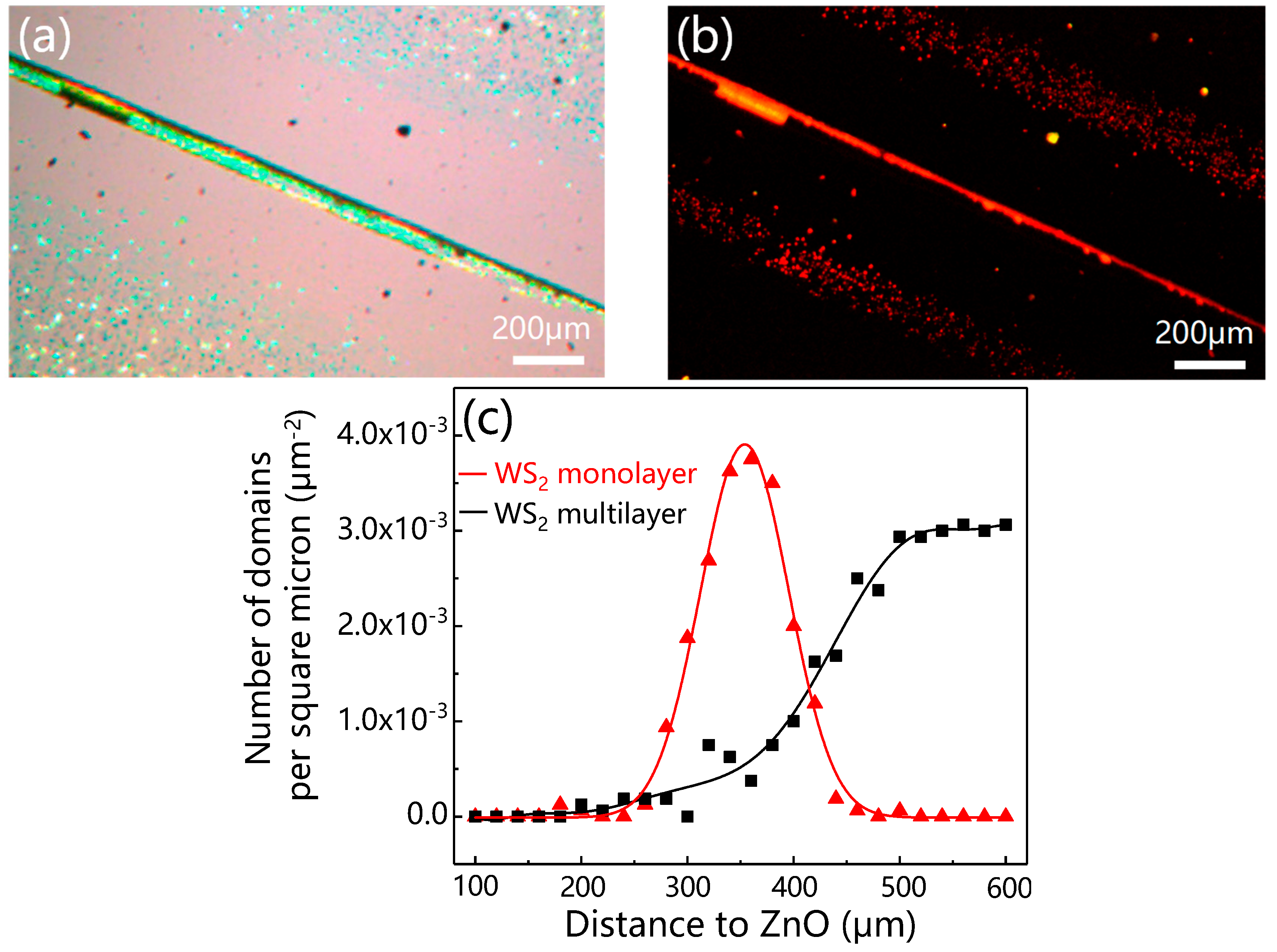
Figure 5a,b shows the optical and PL image of WS2 grown near the region of ZnO whisker, respectively. To investigate the influence of ZnO crystal whisker on the growth of WS2 monolayer, we made distribution statistics of the WS2 monolayer and multilayer at one side of the ZnO crystal whisker. Figure 5c shows the distribution of statistical estimates of the WS2 domain density on the substrate. The direction of the horizontal axis is perpendicular to the growth axis of ZnO whisker. The coordinate of the ZnO whisker on the horizontal axis is zero.
WS2 domains hardly grew in the region (0–250 μm) close to the ZnO whisker. In the region (250–450 μm), a little farther away from the WS2 whisker, monolayer WS2 domains symmetrically grew on both sides of the ZnO crystal whisker, suggesting the ZnO crystal whisker played a crucial role in the growth of the WS2 monolayer. In the region (larger than 450 μm) far away from the ZnO whisker, where ZnO has hardly any impact on the growth of WS2, multilayer WS2 domains were observed. Therefore, monolayer and multilayers were grown separately in different zones of the substrate. To date, the position control of the WS2 monolayer has not been reported. The merit of our growth method lies in the accurate positioning of the WS2 monolayer using ZnO whisker.
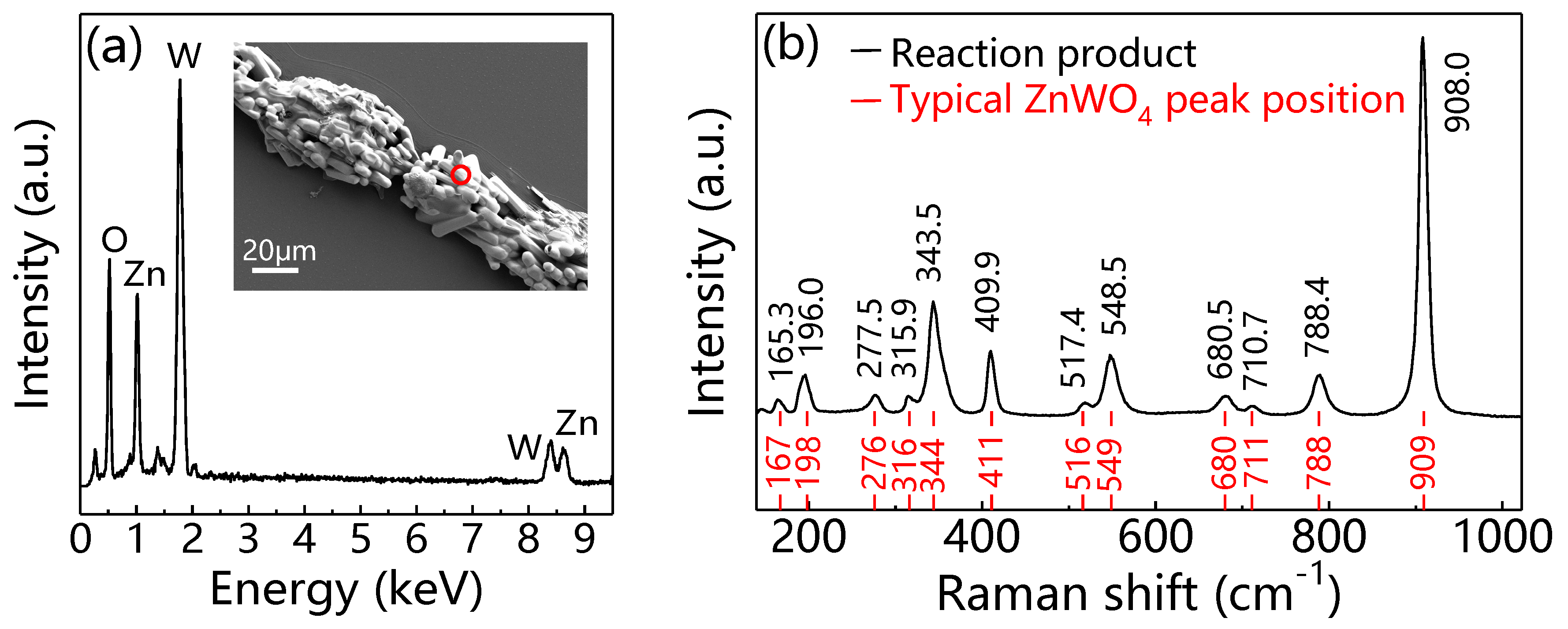
Before analyzing the mechanism of monolayer WS2 growth in the presence of ZnO, we characterized the product of ZnO after WS2 growth by SEM, EDS, and Raman spectra. Besides oxygen and zinc, we found tungsten (W) element in the sample. The EDS spectrum intensity of W is even greater than that of Zn. In addition, the morphology transformed from the crystal whisker of ZnO to capsules as shown in the insert of Figure 6a. The results of EDS and SEM indicate that the chemical composition of the ZnO whisker may have been changed after the growth of WS2. Raman results further verified our assumption. Figure 6b is the Raman spectrum of ZnO crystal whisker after WS2 deposition. We find all the Raman peaks are due to ZnWO4. The slight difference of Raman peak position between our experiment and the reference may lie in the test conditions and/or strain in the sample. Therefore, ZnO transformed into ZnWO4 during the growth of WS2 domains.
At the high temperature of 1000 °C and low pressure of 70 torr, WS2 powder evaporated and decomposed into W and S atoms. According to the elementary composition of reaction product ZnWO4, W atoms reacted with ZnO and were consumed resulting in the depletion region of W atoms and the S-rich region around ZnO.
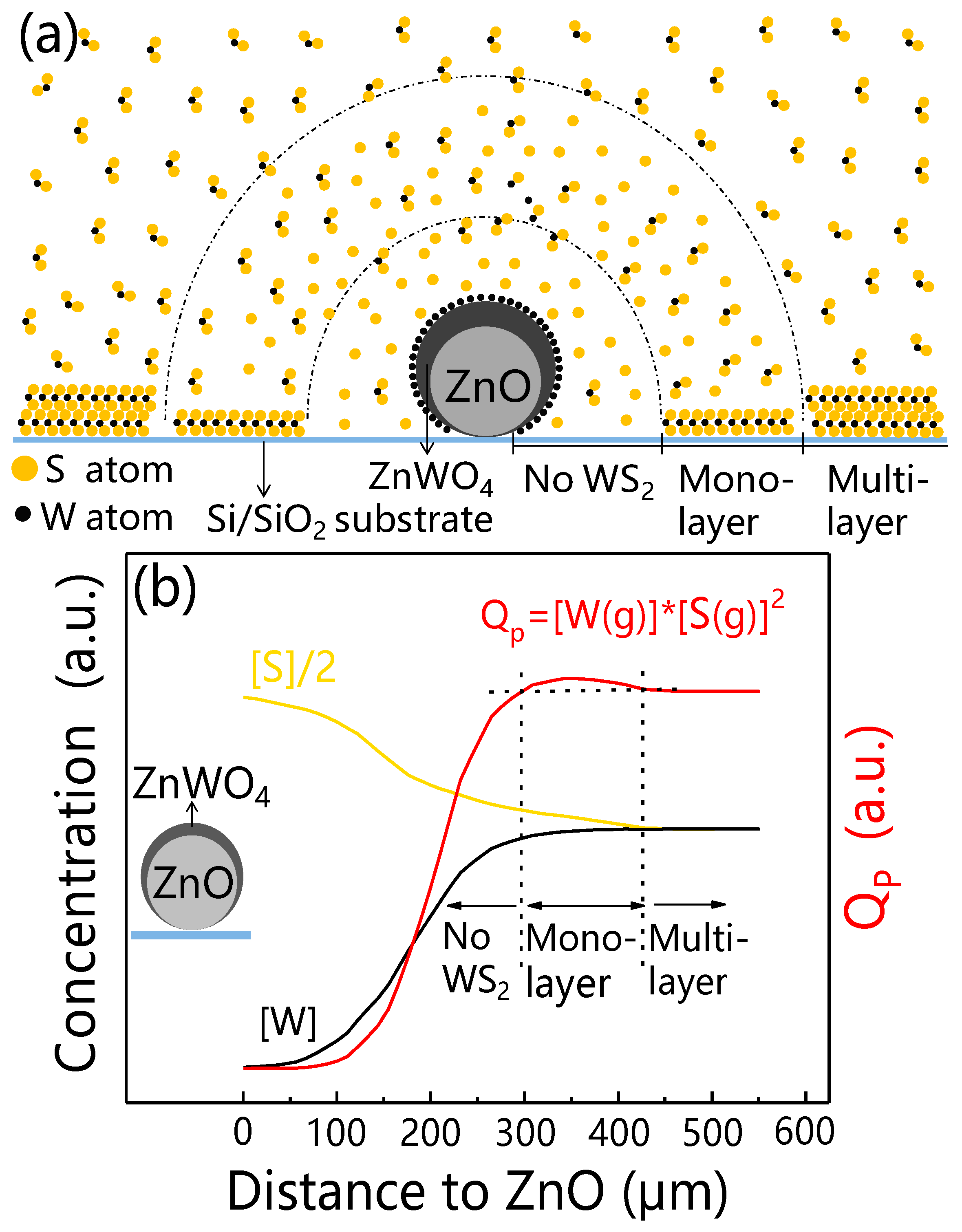
To discuss the growth mechanism, we built a distance dependent model of W and S distribution and WS2 domain growth. Figure 7a shows a schematic diagram of W and S distribution around ZnO crystal whisker. Figure 7b shows the distribution of estimates of W and S atoms concentration around the ZnO whisker. The direction of the horizontal axis is perpendicular to the growth axis of ZnO whisker. The coordinate of the ZnO whisker on the horizontal axis is zero.
In the area far from the ZnO (larger than 450 μm), the growth of WS2 is barely influenced by ZnO. In this area, multilayer WS2 domains are grown. We consider the deposition of WS2 domains achieves chemical equilibrium. The equilibrium constant is denoted as KC.
In the area (0–450 μm) close to ZnO crystal whisker, W atoms reacted with ZnO to form ZnWO4 resulting in a decrease of the W atom concentration. WS2 precursors far from this area will diffuse to this region to keep the reaction running. With the reaction and diffusion of the WS2 precursor, W atoms are consumed and S atoms are accumulated in this area. With the distance increase, the W atom concentration increases and the S atom concentration decreases. They all reach equilibrium concentration when the distance is larger than 450 μm. Reaction quotient (QP) increases first, and reaches the maximum value (250–450 μm), then decreases to the equilibrium constant KC. In the area of 0–250 μm to ZnO crystal whisker, the W atom concentration is low and the reaction quotient QP is no more than KC. Therefore, the WS2 domains hardly grow. In the area of 250–450 μm to ZnO crystal whisker, the larger QP (>KC) and S atom concentration promote the growth of monolayer WS2. The excess S atom is the key parameter for the monolayer growth.
4. Conclusions
In summary, we successfully prepared monolayer WS2 by a novel method. ZnO crystal whisker was used to position and promote the growth of WS2. The distribution statistics show monolayer WS2 was grown on both sides of the ZnO crystal whisker. By constructing a concentration distribution model, we were able to discuss the monolayer growth mechanism. The results reveal that gaseous sulfur and tungsten concentration are crucial for the thickness control of WS2. Higher concentration of sulfur and lower concentration of tungsten are of tremendous benefit for monolayer WS2 growth. This method would provide a way to grow and pattern monolayer WS2 and other two dimensional transition metal disulfides on silicon substrate for the fabrication of nano-optoelectronic devices.
Author Contributions
Y.L. and G.W. conceived and designed the experiments and wrote the paper; Z.X. and F.H. performed the experiments and wrote the paper; C.Z. and S.Z. analyzed the data and wrote the paper.
Funding
This work was supported by the Natural Science Foundation of Zhejiang Province, China Projects (LY16E020008) and Chinese NSF Projects (61106100).
Conflicts of Interest
The authors declare no conflict of interest.
References
- Song, L.; Ci, L.; Lu, H.; Sorokin, P.B.; Jin, C.; Ni, J.; Kvashnin, A.G.; Kvashnin, D.G.; Lou, J.; Yakobson, B.I.; et al. Large Scale Growth and Characterization of Atomic Hexagonal Boron Nitride Layers. Nano Lett. 2010, 10, 3209–3215. [Google Scholar] [CrossRef]
- Geim, A.K.; Novoselov, K.S. The rise of graphene. Nat. Mater. 2007, 6, 183–191. [Google Scholar] [CrossRef] [PubMed]
- Wang, Q.H.; Kalantar-Zadeh, K.; Kis, A.; Coleman, J.N.; Strano, M.S. Electronics and optoelectronics of two-dimensional transition metal dichalcogenides. Nat. Nanotechnol. 2012, 7, 699–712. [Google Scholar] [CrossRef] [PubMed]
- Xue, Y.; Zhang, Y.; Liu, Y.; Liu, H.; Song, J.; Sophia, J.; Liu, J.; Xu, Z.; Xu, Q.; Wang, Z.; et al. Scalable Production of a Few-Layer MoS2/WS2 Vertical Heterojunction Array and Its Application for Photodetectors. ACS Nano 2016, 10, 573–580. [Google Scholar] [CrossRef] [PubMed]
- Liu, Y.; Weiss, N.O.; Duan, X.; Cheng, H.; Huang, Y.; Duan, X. Van der Waals heterostructures and devices. Nat. Rev. Mater. 2016, 1, 160429. [Google Scholar] [CrossRef]
- Perea-Lopez, N.; Elias, A.L.; Berkdemir, A.; Castro-Beltran, A.; Gutierrez, H.R.; Feng, S.; Lv, R.; Hayashi, T.; Lopez-Urias, F.; Ghosh, S.; et al. Photosensor Device Based on Few-Layered WS2 Films. Adv. Funct. Mater. 2013, 23, 5511–5517. [Google Scholar] [CrossRef]
- Ma, X.L.; Zhang, R.J.; An, C.H.; Wu, S.; Hu, X.D.; Liu, J. Efficient doping modulation of monolayer WS2 for optoelectronic applications. Chin. Phys. B 2019, 28, 037803. [Google Scholar] [CrossRef]
- Fiori, G.; Bonaccorso, F.; Iannaccone, G.; Palacios, T.; Neumaier, D.; Seabaugh, A.; Banerjee, S.K.; Colombo, L. Electronics based on two-dimensional materials. Nat. Nanotechnol. 2014, 9, 768–779. [Google Scholar] [CrossRef]
- Therese, H.A.; Li, J.X.; Kolb, U.; Tremel, W. Facile large scale synthesis of WS2 nanotubes from WO3 nanorods prepared by a hydrothermal route. Solid State Sci. 2005, 7, 67–72. [Google Scholar] [CrossRef]
- Coleman, J.N.; Lotya, M.; O’Neill, A.; Bergin, S.D.; King, P.J.; Khan, U.; Young, K.; Gaucher, A.; De, S.; Smith, R.J.; et al. Two-Dimensional Nanosheets Produced by Liquid Exfoliation of Layered Materials. Science 2011, 331, 568–571. [Google Scholar] [CrossRef] [Green Version]
- Biccai, S.; Barwich, S.; Boland, D.; Harvey, A.; Hanlon, D.; McEvoy, N.; Coleman, J.N. Exfoliation of 2D materials by high shear mixing. 2D Mater. 2019, 6, 0150081. [Google Scholar] [CrossRef]
- Lv, R.; Robinson, J.A.; Schaak, R.E.; Sun, D.; Sun, Y.; Mallouk, T.E.; Terrones, M. Transition Metal Dichalcogenides and Beyond: Synthesis, Properties, and Applications of Single- and Few-Layer Nanosheets. Acc. Chem. Res. 2015, 48, 56–64. [Google Scholar] [CrossRef] [PubMed]
- Lan, C.; Li, C.; Yin, Y.; Liu, Y. Large-area synthesis of monolayer WS2 and its ambient-sensitive photo-detecting performance. Nanoscale 2015, 7, 5974–5980. [Google Scholar] [CrossRef] [PubMed]
- Yun, S.J.; Chae, S.H.; Kim, H.; Park, J.C.; Park, J.; Han, G.H.; Lee, J.S.; Kim, S.M.; Oh, H.M.; Seok, J.; et al. Synthesis of Centimeter-Scale Monolayer Tungsten Disulfide Film on Gold Foils. ACS Nano 2015, 9, 5510–5519. [Google Scholar] [CrossRef] [PubMed]
- Joo, M.; Yun, Y.; Yun, S.; Lee, Y.H.; Suh, D. Strong Coulomb scattering effects on low frequency noise in monolayer WS2 field-effect transistors. Appl. Phys. Lett. 2016, 109, 153102. [Google Scholar] [CrossRef]
- Forcherio, G.T.; Bonacina, L.; Riporto, J.; Mugnier, Y.; Le Dantec, R.; Dunklin, J.R.; Benamara, M.; Roper, D.K. Integrating plasmonic metals and 2D transition metal dichalcogenides for enhanced nonlinear frequency conversion. In Physical Chemistry of Semiconductor Materials and Interfaces XVII, Proceedings of the SPIE 2018, San Diego, CA, USA, 20–23 August 2018; Bronstein, H.A., Deschler, F., Kirchartz, T., Eds.; SPIE: Bellingham, WA, USA, 2018. [Google Scholar]
- Liu, P.; Luo, T.; Xing, J.; Xu, H.; Hao, H.; Liu, H.; Dong, J. Large-Area WS2 Film with Big Single Domains Grown by Chemical Vapor Deposition. Nanoscale Res. Lett. 2017, 12, 558. [Google Scholar] [CrossRef] [PubMed]
- O’Brien, M.; McEvoy, N.; Hanlon, D.; Hallam, T.; Coleman, J.N.; Duesberg, G.S. Mapping of Low-Frequency Raman Modes in CVD-Grown Transition Metal Dichalcogenides: Layer Number, Stacking Orientation and Resonant Effects. Sci. Rep. 2016, 6, 19476. [Google Scholar] [CrossRef]
- Cong, C.; Shang, J.; Wu, X.; Cao, B.; Peimyoo, N.; Qiu, C.; Sun, L.; Yu, T. Synthesis and Optical Properties of Large-Area Single-Crystalline 2D Semiconductor WS2 Monolayer from Chemical Vapor Deposition. Adv. Opt. Mater. 2014, 2, 131–136. [Google Scholar] [CrossRef]
- Rajan, A.G.; Warner, J.H.; Blankschtein, D.; Strano, M.S. Generalized mechanistic model for the chemical vapor deposition of 2D transition metal dichalcogenide monolayers. ACS Nano 2016, 10, 4330–4344. [Google Scholar] [CrossRef]
- Shi, Y.; Li, H.; Li, L.-J. Recent Advances in Controlled Synthesis of Two-Dimensional Transition Metal Dichacogenides via Vapour Deposition Techniques. Chem. Soc. Rev. 2015, 44, 2744–2756. [Google Scholar] [CrossRef]
- Zhang, Y.; Zhang, Y.; Ji, Q.; Ju, J.; Yuan, H.; Shi, J.; Gao, T.; Ma, D.; Liu, M.; Chen, Y.; et al. Controlled Growth of High-Quality Monolayer WS2 Layers on Sapphire and Imaging Its Grain Boundary. ACS Nano 2013, 7, 8963–8971. [Google Scholar] [CrossRef] [PubMed]
- Fan, X.; Zhao, Y.; Zheng, W.; Li, H.; Wu, X.; Hu, X.; Zhang, X.; Zhu, X.; Zhang, Q.; Wang, X.; et al. Controllable Growth and Formation Mechanisms of Dislocated WS2 Spirals. Nano Lett. 2018, 18, 3885–3892. [Google Scholar] [CrossRef] [PubMed]
- Cain, J.D.; Shi, F.; Wu, J.; Dravid, V.P. Growth Mechanism of Transition Metal Dichalcogenide Monolayers: The Role of Self-Seeding Fullerene Nuclei. ACS Nano 2016, 10, 5440–5445. [Google Scholar] [CrossRef] [PubMed]
- Ji, Z.; Hao, F.; Wang, C.; Xi, J. Centimetre-long single crystalline ZnO fibres prepared by vapour transportation. Chin. Phys. Lett. 2008, 25, 3467–3469. [Google Scholar]
- Heo, H.; Sung, J.H.; Cha, S.; Jang, B.; Kim, J.; Jin, G.; Lee, D.; Ahn, J.; Lee, M.; Shim, J.H.; et al. Interlayer orientation-dependent light absorption and emission in monolayer semiconductor stacks. Nat. Commun. 2015, 6, 7372. [Google Scholar] [CrossRef]
- Gutierrez, H.R.; Perea-Lopez, N.; Elias, A.L.; Berkdemir, A.; Wang, B.; Lv, R.; Lopez-Urias, F.; Crespi, V.H.; Terrones, H.; Terrones, M. Extraordinary Room-Temperature Photoluminescence in Triangular WS2 Monolayers. Nano Lett. 2013, 13, 3447–3454. [Google Scholar] [CrossRef]
- Wang, X.H.; Ning, J.Q.; Zheng, C.C.; Zhu, B.R.; Xie, L.; Wu, H.S.; Xu, S.J. Photoluminescence and Raman mapping characterization of WS2 monolayers prepared using top-down and bottom-up methods. J. Mater. Chem. C 2015, 3, 2589–2592. [Google Scholar] [CrossRef]
- Berkdemir, A.; Gutierrez, H.R.; Botello-Mendez, A.R.; Perea-Lopez, N.; Elias, A.L.; Chia, C.; Wang, B.; Crespi, V.H.; Lopez-Urias, F.; Charlier, J.; et al. Identification of individual and few layers of WS2 using Raman Spectroscopy. Sci. Rep. 2013, 3, 1755. [Google Scholar] [CrossRef]
- Zhang, X.; Qiao, X.; Shi, W.; Wu, J.; Jiang, D.; Tan, P. Phonon and Raman scattering of two-dimensional transition metal dichalcogenides from monolayer, multilayer to bulk material. Chem. Soc. Rev. 2015, 44, 2757–2785. [Google Scholar] [CrossRef] [Green Version]
- Basiev, T.T.; Karasik, A.Y.; Sobol, A.A.; Chunaev, D.S.; Shukshin, V.E. Spontaneous and stimulated Raman scattering in ZnWO4 crystals. Quantum Electron. 2011, 41, 370–372. [Google Scholar] [CrossRef]
- Huang, G.; Zhu, Y. Synthesis and photocatalytic performance of ZnWO4 catalyst. Mater. Sci. Eng. B-Solid State Mater. Adv. Technol. 2007, 139, 201–208. [Google Scholar] [CrossRef]
Figure 1.
(a) Schematic diagram of the home-built chemical vapor deposition (CVD) system and tungsten disulfide (WS2) after CVD growth. (b) Optical microscopy image of ZnO crystal whisker transferred onto the surface of SiO2/Si substrate before WS2 growth. Insert illustration: cross section of ZnO crystal whisker with a length and width of 67.0 μm and 45.9 μm, respectively.

Figure 2.
Scanning electron microscopy (SEM) image of WS2 grown on SiO2/Si substrate.

Figure 3.
(a) Optical microscopy image of WS2 monolayer (marked with a blue triangle) and multilayer (marked with a red triangle). (b) The photoluminescence (PL) image corresponding to the sample (a). (a,b) are taken at the same location. The pattern with red color in (b) is due to the PL emission of monolayer WS2.

Figure 4.
(a) Raman and (b) PL spectra of WS2 monolayer (red line) and multilayer (black line) corresponding to the WS2 domains in Figure 3a.
Figure 4.
(a) Raman and (b) PL spectra of WS2 monolayer (red line) and multilayer (black line) corresponding to the WS2 domains in Figure 3a.

Figure 5.
(a) The optical image of WS2 domains prepared with the assistance of ZnO whisker. (b) PL image corresponding to the image of (a). (c) WS2 domain distribution is a function of distance from the ZnO whisker. The origin is the ZnO crystal whisker. (a) and (b) were taken at the same location. The straight lines are related to ZnO whisker and the scale bars represent 200 μm.

Figure 6.
(a) EDS and (b) Raman spectra of ZnO crystal whisker after WS2 growth. Insert in (a) is the SEM image with a red circle where the EDS spectrum is taken from. The data in black and red color in (b) correspond to our experiment and reference [31,32], respectively.

Figure 7.
(a) Schematic diagram of W and S distribution around ZnO crystal whisker. (b) Distance dependence of W atom concentration, S atom concentration, and the reaction quotient (QP). The direction of the horizontal axis is perpendicular to the growth axis of ZnO whisker. The coordinate of the ZnO whisker on the horizontal axis is zero. [W] and [S] represent W and S atom concentration in (b), respectively.

© 2019 by the authors. Licensee MDPI, Basel, Switzerland. This article is an open access article distributed under the terms and conditions of the Creative Commons Attribution (CC BY) license (http://creativecommons.org/licenses/by/4.0/).
Share and Cite
MDPI and ACS Style
Xu, Z.; Lv, Y.; Huang, F.; Zhao, C.; Zhao, S.; Wei, G. ZnO-Controlled Growth of Monolayer WS2 through Chemical Vapor Deposition. Materials 2019, 12, 1883. https://doi.org/10.3390/ma12121883
AMA Style
Xu Z, Lv Y, Huang F, Zhao C, Zhao S, Wei G. ZnO-Controlled Growth of Monolayer WS2 through Chemical Vapor Deposition. Materials. 2019; 12(12):1883. https://doi.org/10.3390/ma12121883
Chicago/Turabian StyleXu, Zhuhua, Yanfei Lv, Feng Huang, Cong Zhao, Shichao Zhao, and Guodan Wei. 2019. "ZnO-Controlled Growth of Monolayer WS2 through Chemical Vapor Deposition" Materials 12, no. 12: 1883. https://doi.org/10.3390/ma12121883
Note that from the first issue of 2016, this journal uses article numbers instead of page numbers. See further details here.