One-Step Synthesis of Silver Nanowires with Ultra-Long Length and Thin Diameter to Make Flexible Transparent Conductive Films

Abstract
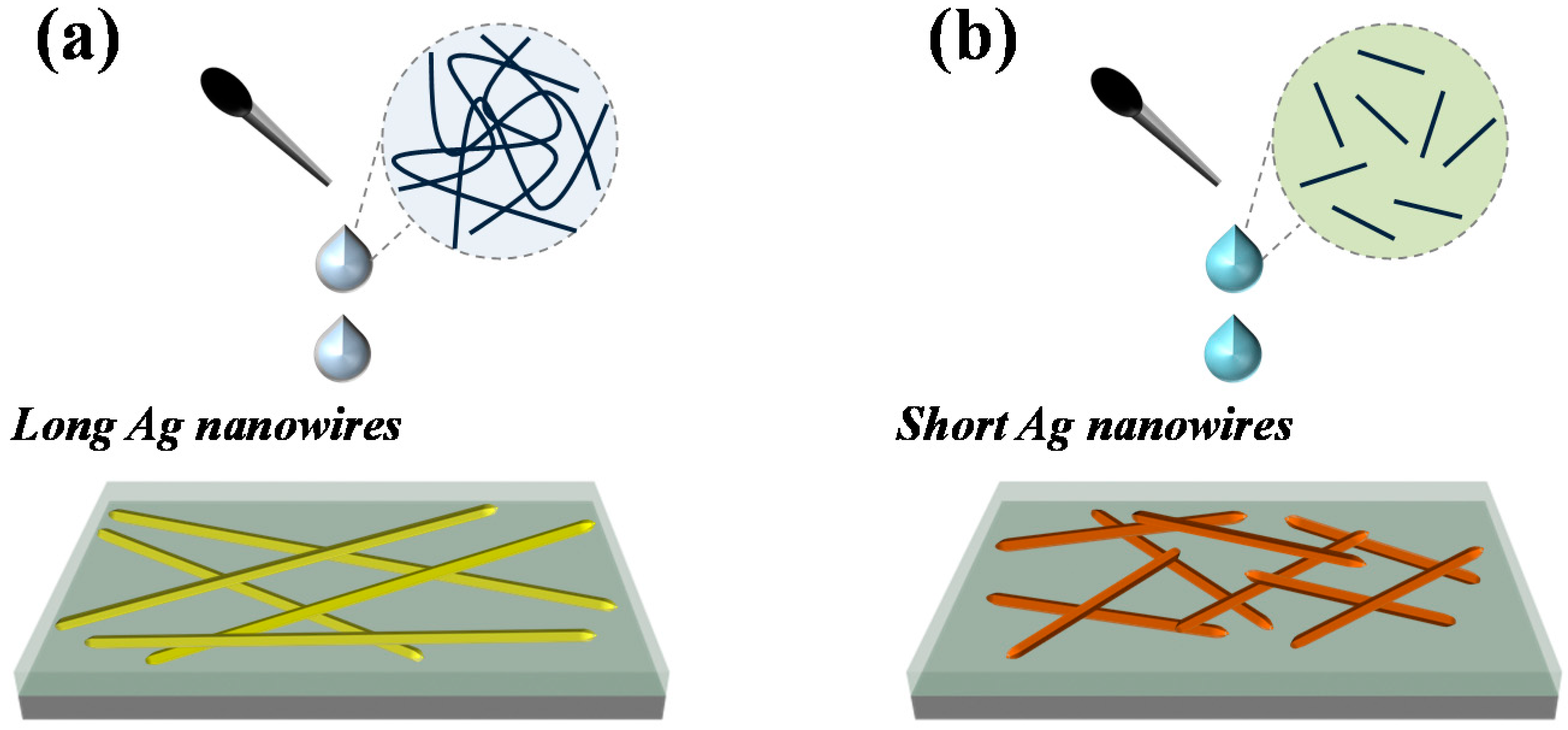
:
1. Introduction
2. Materials and Methods
2.1. Materials
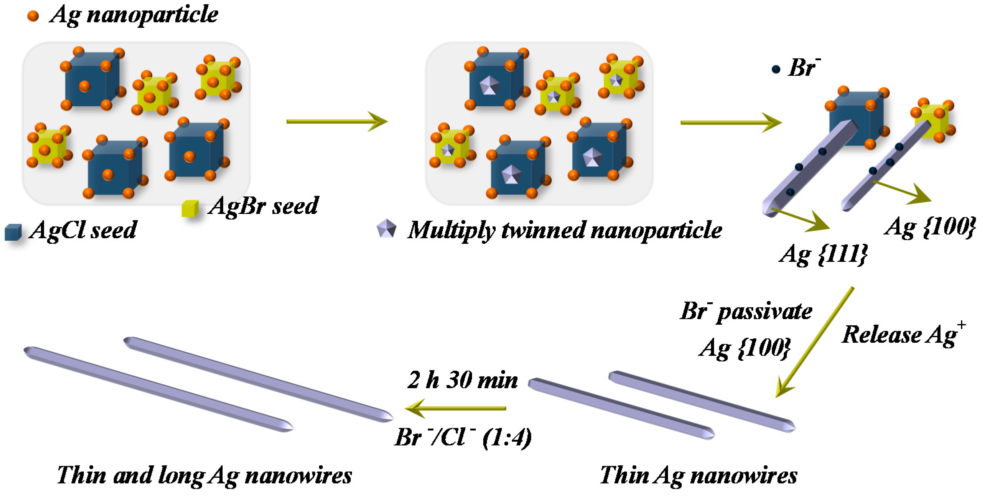
2.2. Preparation of Thin and Long AgNWs
2.3. Preparation of AgNW Ink
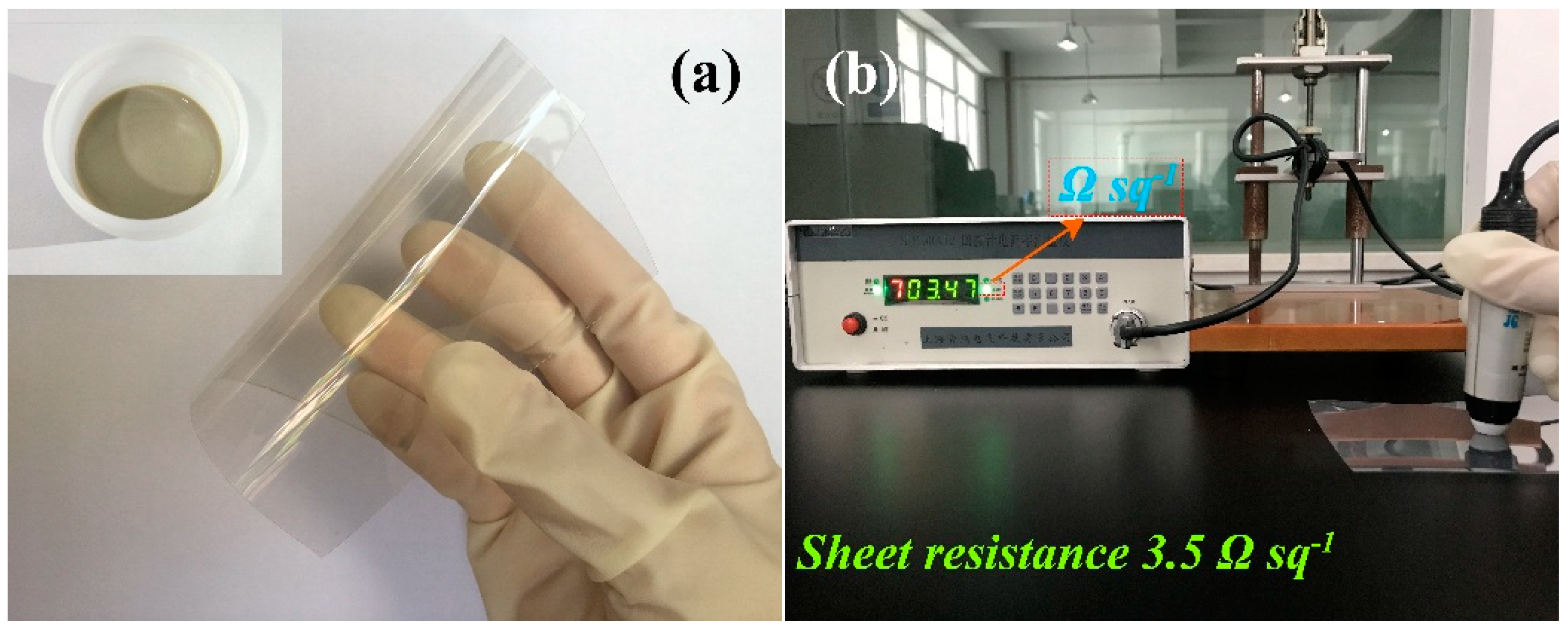
2.4. Fabrication of AgNW-Based TCFs
2.5. Characterization
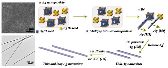
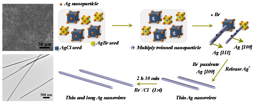
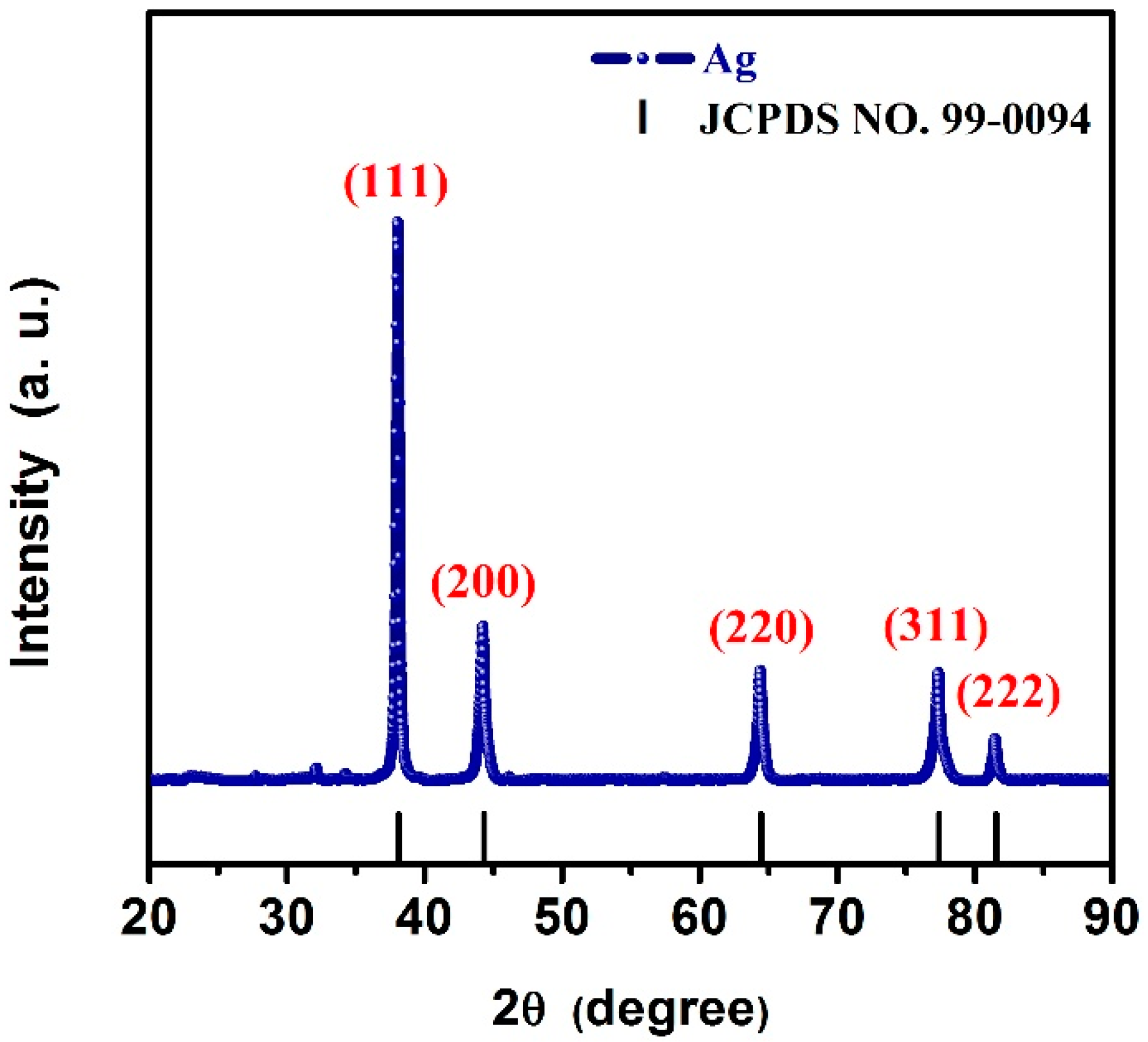
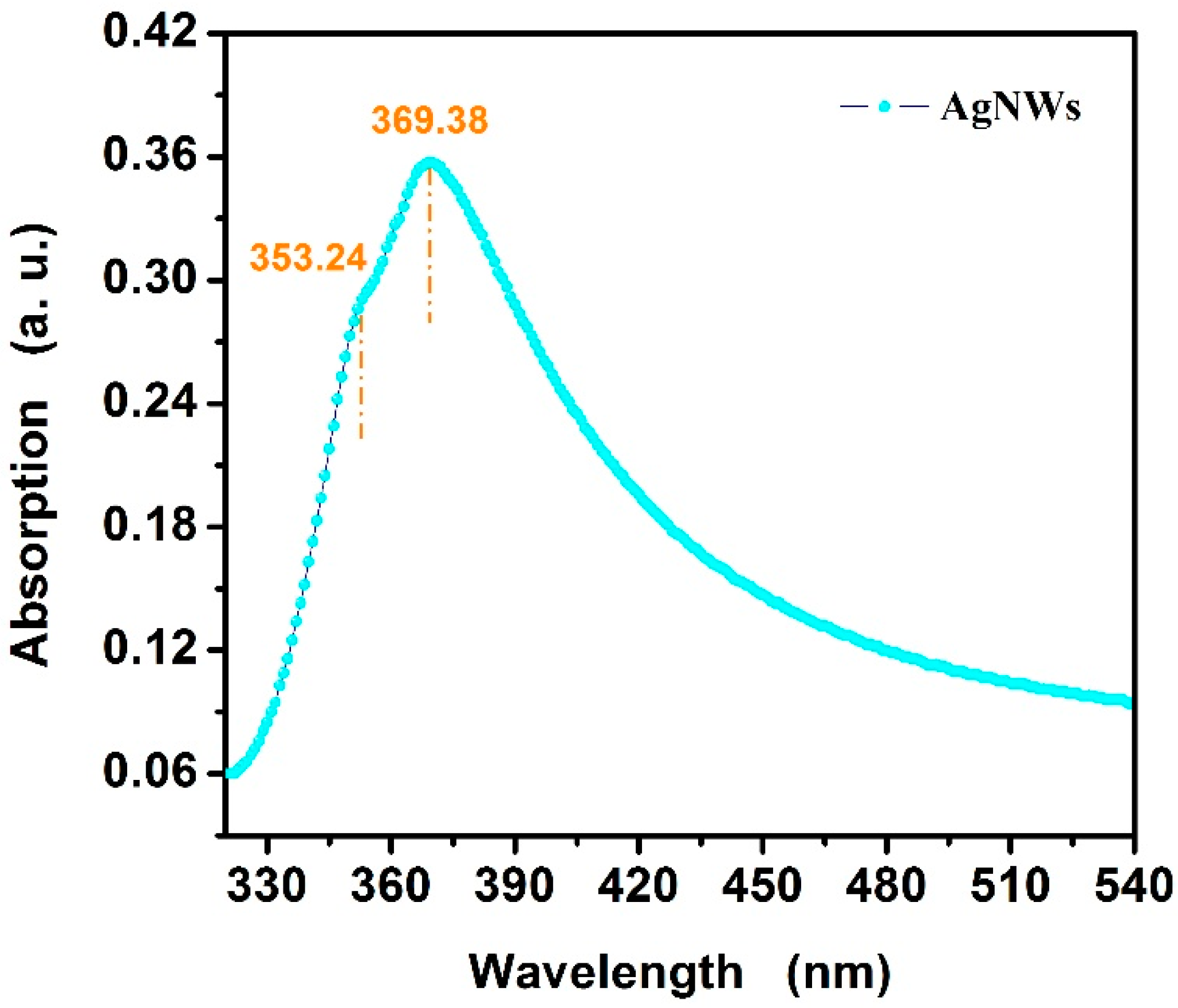
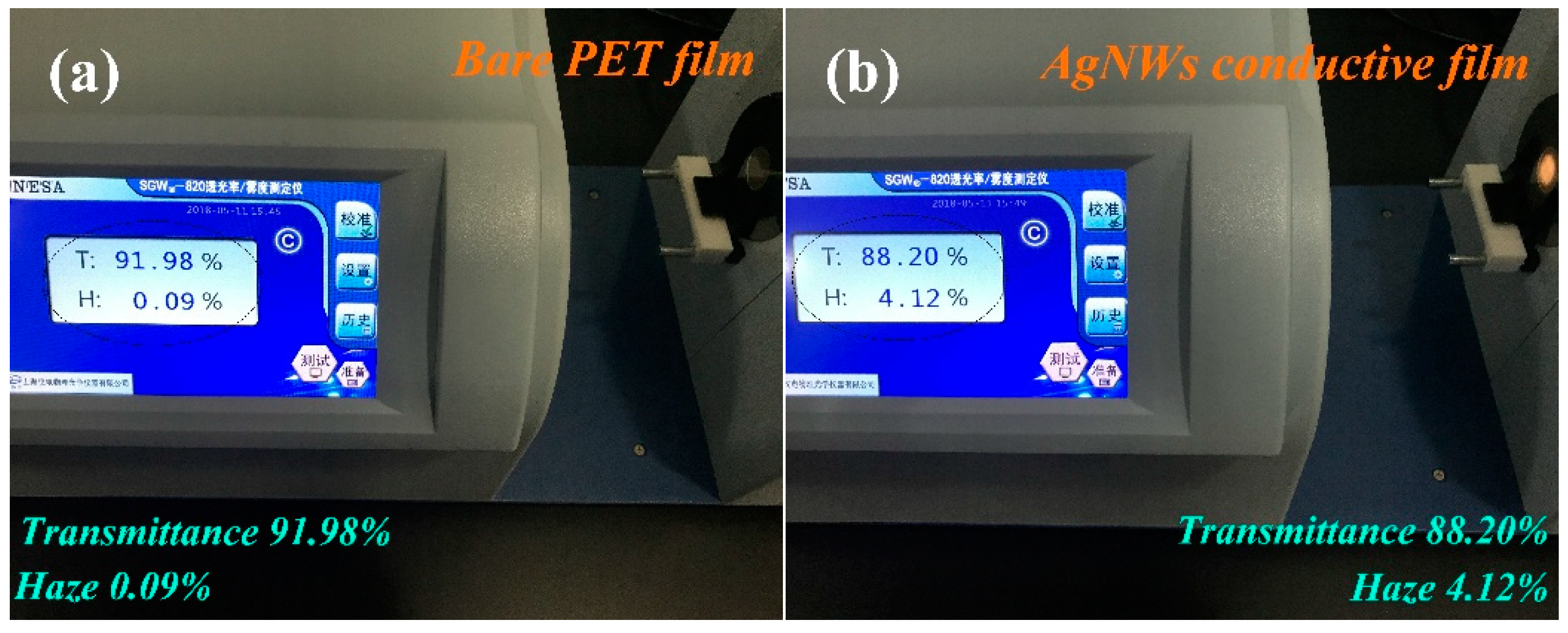
3. Results and Discussion
4. Conclusions
Author Contributions
Funding
Conflicts of Interest
References
- Wang, Y.; Zhu, C.X.; Pfattner, R.; Yan, H.P.; Jin, L.H.; Chen, S.C.; Molina-Lopez, F.; Lissel, F.; Liu, J.; Rabiah, N.I.; et al. A highly stretchable, transparent, and conductive polymer. Sci. Adv. 2017, 3, e1602076. [Google Scholar] [CrossRef] [PubMed] [Green Version]
- Chebotareva, A.B.; Untila, G.G.; Kost, T.N.; Stepanov, A.S.; Salazkin, S.N.; Shaposhnikova, V.V. Transparent conductive polymers for laminated multi-wire metallization of bifacial concentrator crystalline silicon solar cells with TCO layers. Sol. Energy Mater. Sol. C 2017, 165, 1–8. [Google Scholar] [CrossRef]
- Jun, S.; Ju, B.K.; Kim, J.W. Fabrication of substrate-free double-side emitting flexible device based on silver nanowire-polymer composite electrode. Curr. Appl. Phys. 2017, 17, 6–10. [Google Scholar] [CrossRef]
- Yang, H.; Chen, T.R.; Wang, H.F.; Bai, S.C.; Guo, X.Z. One-pot rapid synthesis of high aspect ratio silver nanowires for transparent conductive electrodes. Mater. Res. Bull. 2018, 102, 79–85. [Google Scholar] [CrossRef]
- Cui, Z.; Han, Y.; Huang, Q.; Dong, J.; Zhu, Y. Electrohydrodynamic printing of silver nanowires for flexible and stretchable electronics. Nanoscale 2018, 10, 6806–6811. [Google Scholar] [CrossRef] [PubMed]
- Zhang, L.W.; Ji, Y.; Qiu, Y.J.; Xu, C.W.; Liu, Z.G.; Guo, Q.Q. Highly thermal-stable and transparent silver nanowire conductive films via magnetic assisted electrodeposition of Ni. J. Mater. Chem. C 2018, 6, 4887–4894. [Google Scholar] [CrossRef]
- Yang, J.; Bao, C.; Zhu, K.; Yu, T.; Xu, Q. High-performance transparent conducting metal network electrodes for perovksite photodetectors. ACS Appl. Mater. Interfaces 2018, 10, 1996–2003. [Google Scholar] [CrossRef]
- Li, L.; Zhang, B.; Zou, B.; Xie, R.; Zhang, T.; Li, S.; Zheng, B.; Wu, J.; Weng, J.; Zhang, W.; et al. Fabrication of flexible transparent electrode with enhanced conductivity from hierarchical metal grids. ACS Appl. Mater. Interfaces 2017, 9, 39110–39115. [Google Scholar] [CrossRef]
- Savchak, M.; Borodinov, N.; Burtovyy, R.; Anayee, M.; Hu, K.; Ma, R.; Grant, A.; Li, H.; Cutshall, D.B.; Wen, Y.; et al. Highly conductive and transparent reduced graphene oxide nanoscale films via thermal conversion of polymer-encapsulated graphene oxide sheets. ACS Appl. Mater. Interfaces 2018, 10, 3975–3985. [Google Scholar] [CrossRef]
- Ning, J.; Hao, L.; Jin, M.; Qiu, X.; Shen, Y.; Liang, J.; Zhang, X.; Wang, B.; Li, X.; Zhi, L. A facile reduction method for roll-to roll production of high performance graphene-based transparent conductive films. Adv. Mater. 2017, 29, 1605028. [Google Scholar] [CrossRef]
- Zhao, F.G.; Kong, Y.T.; Xu, Z.W.; Yao, X.; Zuo, B.; Li, W.S. High-performance flexible transparent conductive films achieved by cooperation between 1D copper nanowires and 2D graphene materials. J. Mater. Chem. C 2017, 5, 5509–5526. [Google Scholar] [CrossRef]
- Zhang, L.Q.; Yang, R.; Chen, K.; Wang, X.; Tang, Y.S.; Yang, F.; Rui, L.; Ye, Z.Z.; Li, Y.F. The fabrication of Cu nanowire/graphene/Al doped ZnO transparent conductive film on PET substrate with high flexibility and air stability. Mater. Lett. 2017, 207, 62–65. [Google Scholar] [CrossRef]
- Urper, O.; Cakmak, I.; Karatepe, N. Fabrication of carbon nanotube transparent conductive films by vacuum filtration method. Mater. Lett. 2018, 223, 210–214. [Google Scholar] [CrossRef]
- He, Y.; Jin, H.; Qiu, S.; Li, Q. A novel strategy for high-performance transparent conductive films based on double-walled carbon nanotubes. Chem. Commun. 2017, 53, 2934–2937. [Google Scholar]
- Li, J.; Otsuka, K.; Zhang, X.; Maruyama, S.; Liu, J. Selective synthesis of large diameter, highly conductive and high density single-walled carbon nanotubes by a thiophene-assisted chemical vapor deposition method on transparent substrates. Nanoscale 2016, 8, 14156–14162. [Google Scholar] [CrossRef]
- Yang, X.; Hu, X.; Wang, Q.; Xiong, J.; Yang, H.; Meng, X.; Tan, L.; Chen, L.; Chen, Y. Large-scale stretchable semiembedded copper nanowire transparent conductive films by an electrospinning template. ACS Appl. Mater. Interfaces 2017, 9, 26468–26475. [Google Scholar] [CrossRef]
- Ahn, Y.; Jeong, Y.; Lee, D.; Lee, Y. Copper nanowire-graphene core-shell nanostructure for highly stable transparent conducting electrodes. ACS Nano 2015, 9, 3125–3133. [Google Scholar] [CrossRef]
- Shin, D.K.; Park, J. Suppression of moire phenomenon induced by metal grids for touch screen panels. J. Disp. Technol. 2016, 12. [Google Scholar] [CrossRef]
- Du, G.; Wang, Y.; Lu, Z.Q.; Yang, F.; Wang, X.; Liu, L.F.; Han, D.D.; Wang, Y.; Xing, Z.; Kang, J.F. High performance of large-sized dye sensitized solar cells based on a novel low-cost metal girds manufactured process. Solid-State Integr. Circ. Technol. 2012. [Google Scholar] [CrossRef]
- Kwon, J.; Suh, Y.D.; Lee, J.; Lee, P.; Han, S.; Hong, S.; Yeo, J.; Lee, H.; Ko, S.H. Recent progress in silver nanowire based flexible/wearable optoelectronics. J. Mater. Chem. C 2018, 6, 7445–7461. [Google Scholar] [CrossRef]
- Huang, Q.J.; Zhu, Y. Gravure printing of water-based silver nanowire ink on plastic substrate for flexible electronics. Sci. Rep. 2018, 8, 15167. [Google Scholar] [CrossRef]
- Jiu, J.; Araki, T.; Wang, J.; Nogi, M.; Sugahara, T.; Nagao, S.; Koga, H.; Suganuma, K.; Nakazawa, E.; Hara, M.; et al. Facile synthesis of very-long silver nanowires for transparent electrodes. J. Mater. Chem. A 2014, 2, 6326–6330. [Google Scholar] [CrossRef]
- Kim, T.; Canlier, A.; Kim, G.H.; Choi, J.; Park, M.; Han, S.M. Electrostatic spray deposition of highly transparent silver nanowire electrode on flexible substrate. ACS Appl. Mater. Interfaces 2013, 5, 788–794. [Google Scholar] [CrossRef] [PubMed]
- Atwa, Y.; Maheshwari, N.; Goldthorpe, I.A. Silver nanowire coated threads for electrically conductive textiles. J. Mater. Chem. C 2015, 3, 3908–3912. [Google Scholar] [CrossRef] [Green Version]
- Lee, E.J.; Chang, M.H.; Kim, Y.S.; Kim, J.Y. High-pressure polyol synthesis of ultrathin silver nanowires: Electrical and optical properties. APL Mater. 2013, 1, 042118. [Google Scholar] [CrossRef] [Green Version]
- Zhang, K.L.; Du, Y.G.; Chen, S.M. Sub 30 nm silver nanowire synthesized using KBr as co-nucleant through one-pot polyol method for optoelectronic applications. Org. Electron. 2015, 26, 380–385. [Google Scholar] [CrossRef]
- Wan, M.J.; Tao, J.Q.; Jia, D.; Chu, X.K.; Li, S.X.; Ji, S.L.; Ye, C.H. High-purity very thin silver nanowires obtained by Ostwald ripening-driven coarsening and sedimentation of nanoparticles. CrystEngComm 2018, 20, 2834–2840. [Google Scholar] [CrossRef]
- Li, B.; Ye, S.G.; Stewart, I.E.; Alvarez, S.; Wiley, B.J. Synthesis and purification of silver nanowires to make conducting films with a transmittance of 99%. Nano Lett. 2015, 15, 6722–6726. [Google Scholar] [CrossRef]
- Zhang, P.; Wei, Y.L.; Ou, M.; Huang, Z.Z.; Lin, S.D.; Tu, Y.Y.; Hu, J. Behind the role of bromide ions in the synthesis of ultrathin silver nanowires. Mater. Lett. 2018, 213, 23–26. [Google Scholar] [CrossRef]
- Du, H.W.; Wan, T.; Qu, B.; Cao, F.Y.; Lin, Q.R.; Chen, N.; Lin, X.; Chu, D.W. Engineering silver nanowire networks: From transparent electrodes to resistive switching devices. ACS Appl. Mater. Interfaces 2017, 9, 20762–20770. [Google Scholar] [CrossRef]
- Alducin, D.; Borja, R.; Ortega, E.; Velazquez-Salazar, J.J.; Covarrubias, M.; Santoyo, F.M.; Bazan-Diaz, L.; Sanchez, J.E.; Torres, N.; Ponce, A.; et al. In situ transmission electron microscopy mechanical deformation and fracture of a silver nanowire. Scr. Mater. 2016, 113, 63–67. [Google Scholar] [CrossRef] [Green Version]
- Chen, C.; Wang, L.; Jiang, G.H.; Zhou, J.F.; Chen, X.; Yu, H.J.; Yang, Q. Study on the synthesis of silver nanowires with adjustable diameters through the polyol process. Nanotechnology 2006, 17, 3933. [Google Scholar] [CrossRef]
- Andres, L.J.; Menendez, M.F.; Gomez, D.; Martinez, A.L.; Bristow, N.; Kettle, J.P.; Menendez, A.; Ruiz, B. Rapid synthesis of ultra-long silver nanowires for tailor-made transparent conductive electrodes: Proof of concept in organic solar cells. Nanotechnology 2015, 26, 265201. [Google Scholar] [CrossRef] [PubMed]
- Silva, R.R.D.; Yang, M.X.; Choi, S.I.; Chi, M.F.; Luo, M.; Zhang, C.; Li, Z.Y.; Camargo, P.H.C.; Ribeiro, S.J.L.; Xia, Y.N. Facile synthesis of sub-20 nm silver nanowires through a bromide-mediated polyol method. ACS Nano 2016, 10, 7892–7900. [Google Scholar] [CrossRef] [PubMed]
- Lee, E.J.; Kim, Y.H.; Hwang, D.K.; Choi, W.K.; Kim, J.Y. Synthesis and optoelectronic characteristics of 20-nm-diameter silver nanowires for highly transparent electrode films. RSC Adv. 2016, 6, 11702–11710. [Google Scholar] [CrossRef]
- Zhou, W.P.; Hu, A.; Bai, S.; Ma, Y.; Bridges, D. Anisotropic optical properties of large-scale aligned silver nanowire films via controlled coffee ring effects. RSC Adv. 2015, 5, 39103–39109. [Google Scholar] [CrossRef]
- Luu, Q.N.; Doorn, J.M.; Berry, M.T.; Jiang, C.Y.; Lin, C.K.; May, P.S. Preparation and optical properties of silver nanowires and silver-nanowire thin films. J. Colloid Interfaces Sci. 2011, 356, 151–158. [Google Scholar] [CrossRef]
- Lee, J.H.; Huynh-Nguyen, B.C.; Ko, E.; Kim, J.H.; Seong, G.H. Fabrication of flexible, transparent silver nanowire electrodes for amperometric detection of hydrogen peroxide. Sens. Actuators B Chem. 2016, 224, 789–797. [Google Scholar] [CrossRef]
- Lim, J.W.; Cho, D.Y.; Kim, J.; Na, S.I.; Kim, H.K. Simple brush-painting of flexible and transparent Ag nanowire network electrodes as an alternative ITO anode for cost-effcient flexible organic solar cells. Sol. Energy Mater. Sol. C 2012, 107, 348–354. [Google Scholar] [CrossRef]
- Jia, Y.G.; Chen, C.; Jia, D.; Li, S.X.; Ji, S.L.; Ye, C.H. Silver nanowire transparent conductive films with high uniformity fabricated via a dynamic heating method. ACS Appl. Mater. Interfaces 2016, 8, 9865–9871. [Google Scholar] [CrossRef]
- Kim, J.; Nam, Y.S.; Song, M.H.; Park, H.W. Large pulsed electron beam welded percolation networks of silver nanowires for transparent and flexible electrodes. ACS Appl. Mater. Interfaces 2016, 8, 20938–20945. [Google Scholar] [CrossRef] [PubMed]
- Bergin, S.M.; Chen, Y.H.; Rathmell, A.R.; Charbonneau, P.; Li, Z.Y.; Wiley, B.J. The effect of nanowire length and diameter on the properties of transparent conducting nanowire films. Nanoscale 2012, 4, 1996–2004. [Google Scholar] [CrossRef] [PubMed]
- Sorel, S.; Lyons, P.E.; De, S.; Dickerson, J.C.; Coleman, J.N. The dependence of the optoelectrical properties of silver nanowire networks on nanowire length and diameter. Nanotechnology 2012, 23, 185201. [Google Scholar] [CrossRef] [PubMed]
- Lyubchenko, D.; Anoshkin, I.V.; Raisanen, A.; Nasibulin, A.G.; Nefedova, I.; Nefedov, I. Resistivity and optical transmittance dependence on length and diameter of nanowires in silver nanowire layers in application to transparent conductive coating. Micro Nano Lett. 2016, 11, 343–347. [Google Scholar]


© 2019 by the authors. Licensee MDPI, Basel, Switzerland. This article is an open access article distributed under the terms and conditions of the Creative Commons Attribution (CC BY) license (http://creativecommons.org/licenses/by/4.0/).
Share and Cite
Li, Y.; Yuan, X.; Yang, H.; Chao, Y.; Guo, S.; Wang, C. One-Step Synthesis of Silver Nanowires with Ultra-Long Length and Thin Diameter to Make Flexible Transparent Conductive Films. Materials 2019, 12, 401. https://doi.org/10.3390/ma12030401
Li Y, Yuan X, Yang H, Chao Y, Guo S, Wang C. One-Step Synthesis of Silver Nanowires with Ultra-Long Length and Thin Diameter to Make Flexible Transparent Conductive Films. Materials. 2019; 12(3):401. https://doi.org/10.3390/ma12030401
Chicago/Turabian StyleLi, Yuxiu, Ximin Yuan, Hongwei Yang, Yunxiu Chao, Shuailong Guo, and Chuan Wang. 2019. "One-Step Synthesis of Silver Nanowires with Ultra-Long Length and Thin Diameter to Make Flexible Transparent Conductive Films" Materials 12, no. 3: 401. https://doi.org/10.3390/ma12030401