Study of GaN-Based Thermal Decomposition in Hydrogen Atmospheres for Substrate-Reclamation Processing

1
Department of Industrial Engineering and Management, Da-Yeh University, Changhua 515, Taiwan
2
Bachelor Program for Design and Materials for Medical Equipment and Device, Da-Yeh University, Changhua 515, Taiwan
*
Author to whom correspondence should be addressed.
Materials 2018, 11(11), 2082; https://doi.org/10.3390/ma11112082
Submission received: 29 September 2018
/
Revised: 19 October 2018
/
Accepted: 22 October 2018
/
Published: 24 October 2018
Abstract
:This study investigates the thermal decomposition behavior of GaN-based epilayers on patterned sapphire substrates (GaN-epi/PSSs) in a quartz furnace tube under a hydrogen atmosphere. The GaN-epi/PSS was decomposed under different hydrogen flow rates at 1200 °C, confirming that the hydrogen flow rate influences the decomposition reaction of the GaN-based epilayer. The GaN was completely removed and the thermal decomposition process yielded gallium oxyhydroxide (GaO2H) nanostructures. When observed by transmission electron microscopy (TEM), the GaO2H nanostructures appeared as aggregates of many nanograins sized 2–5 nm. The orientation relationship, microstructure, and formation mechanism of the GaO2H nanostructures were also investigated.
1. Introduction
GaN and its alloys have been widely used in optoelectronic devices such as green- to deep-ultraviolet light-emitting diodes [1,2,3] and photodetectors [4,5,6]. Various GaN-based semiconductors have become commercially available, although the large number of wafers that are scrapped during the manufacturing process remains problematic. It is hoped that reusing the sapphire substrate of epitaxial layers reclaimed from scrapped wafers will reduce the manufacturing costs. For substrate reclamation, thermal decomposition is more suitable than the common chemical mechanical polishing method, because the former is simple and cheap. However, the thermal decomposition behavior of GaN has been little investigated. In 1965, Munir and Searcy [7] investigated the heat of activation of the reaction 2GaN(s) = 2Ga(l) + N2(g). The decomposition of GaN in the presence of H2 was first studied by Thurmond and Logan in the 1970s [8,9]. Later, GaN decomposition in the presence of H2, N2, HCl, and NH3 at different temperatures and pressures was reported [10,11,12,13,14,15,16]. However, in these reports, the decomposition of GaN epilayers was either prohibited, suppressed, or delayed, and the complete GaN decomposition was not extensively studied.
In this study, we investigate the behaviors of GaN-based thermal decomposition under hydrogen atmospheres with different flow rates. We quantify the partial and complete decompositions of the GaN-based layers, and compare the surface morphologies and crystalline phases of the decomposition products. We also explore the mechanism of the GaN-based thermal decomposition under a hydrogen atmosphere.
2. Experimental Procedures
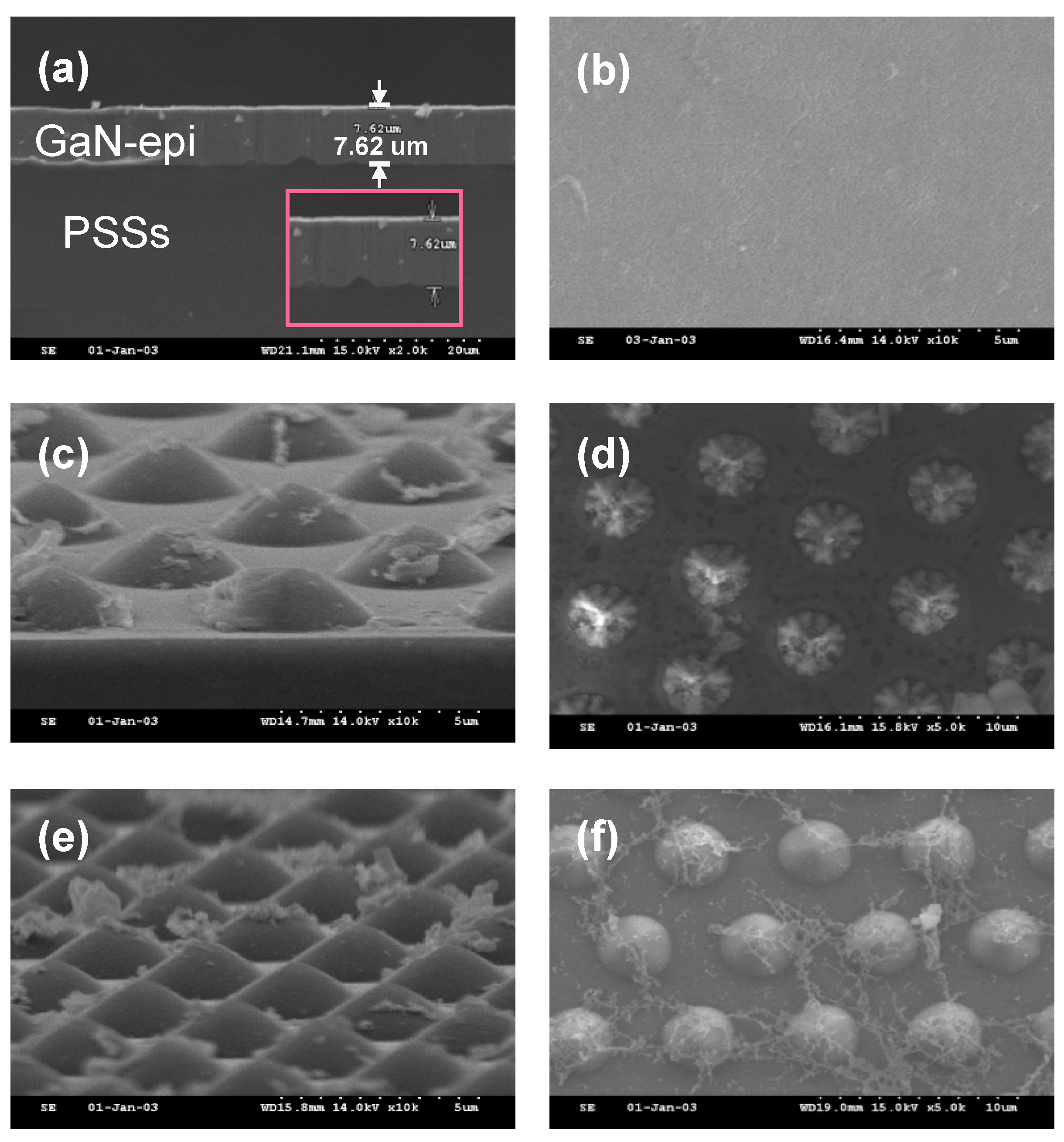
The sample was composed of GaN-based epilayers on patterned sapphire substrates (GaN-epi/PSSs) grown by the standard GaN-epi/PSS fabrication procedure. The original GaN-epi/PSSs was 7.62 μm thick, as shown in Figure 1a. The GaN-epi surfaces were decomposed by loading the sample into a furnace preheated to 1200 °C and filled with hydrogen gas flowing at 0, 10, or 25 cm3/min. The decomposition time was 3 h.
The surface morphologies and compositions of the decomposed GaN-epi/PSS sample were observed with a scanning electron microscopy–energy dispersive spectrometer (SEM–EDS, S-3000H, Hitachi, Tokyo, Japan). The crystal structures of the GaN-epi/PSSs were characterized by X-ray diffraction (XRD; PANalytical, X’Pert Pro MRD System, Malvern Panalytical, Malvern, UK). The XRD radiation source was the Cu Kα line (λ = 1.541874), and the monochromator was Ge (220). The orientation relationships and microstructures of the GaN-epi/PSSs samples were investigated under a transmission electron microscope (TEM) (JEOL JEM-2100F, Tokyo, Japan).
3. Results and Discussion
Figure 1 shows SEM images of the GaN-epi/PSSs morphologies after 3 h in the 1200 °C furnace with different gas-flow rates. Under the gas-flow rate of 10 cm3/min, the thermal decomposition yielded PSS shapes (Figure 1c,d). When the gas-flow rate was increased to 25 cm3/min, the surface shape better resembled an exposed PSS than at 10 cm3/min (Figure 1e,f). These results prove that the decomposition reaction of the GaN-epi/PSSs depended on the hydrogen flow rate. Previously, the GaN decomposition process was found to strongly depend on the temperature and ambient conditions [17]. It is worth noting that the present GaN films were completely decomposed, forming GaO2H on the exposed PSS surface (Figure 1e,f). The GaO2H reactant was confirmed by SEM–EDS and XRD, as discussed below. Later, this phenomenon will be further investigated by the TEM technique.
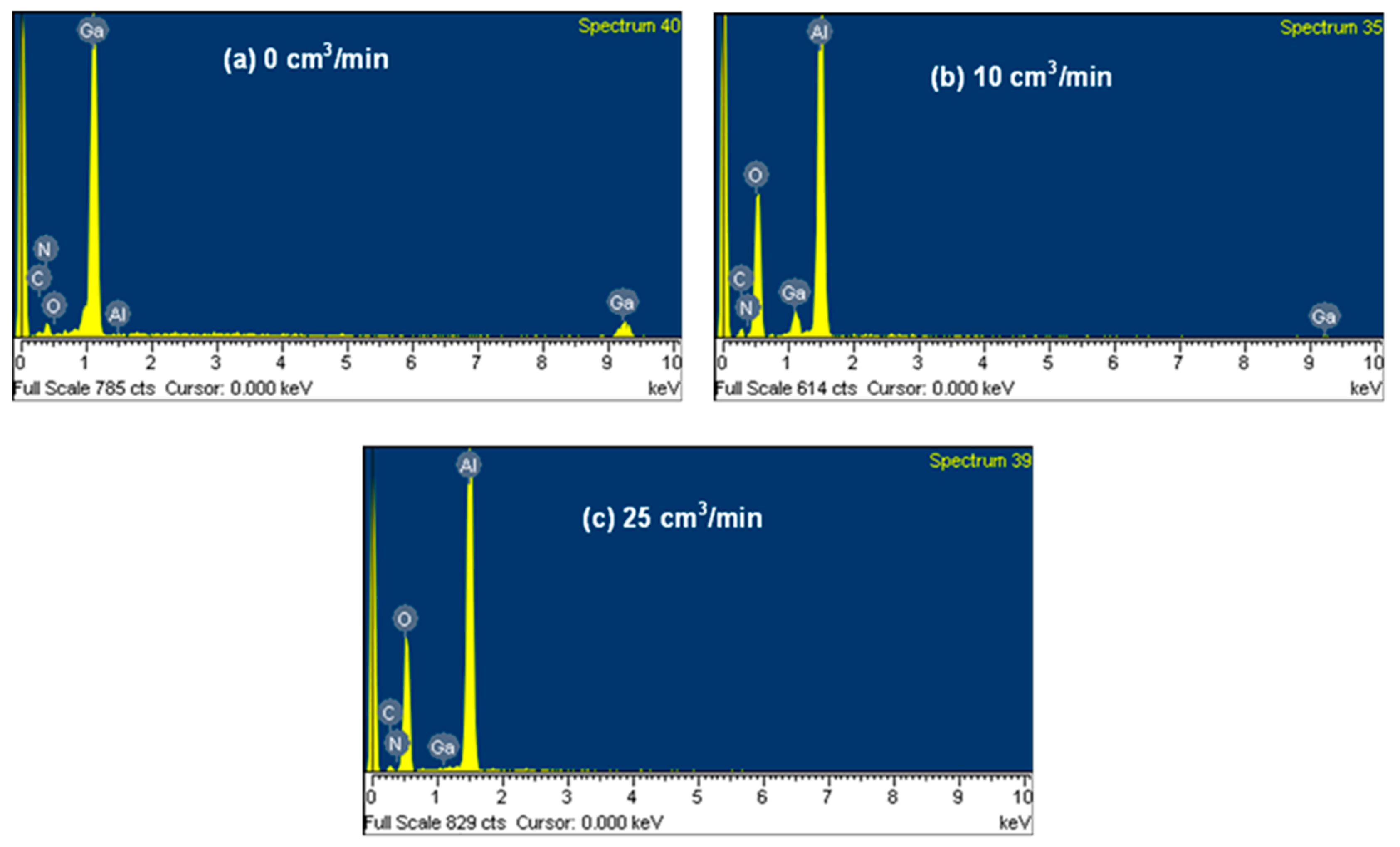
Figure 2 shows the SEM–EDS spectra of the GaN-epi/PSSs decomposed in the 1200 °C furnace under hydrogen flow rates of 0, 10, and 25 cm3/min. In the absence of H2 gas (0 cm3/min), the GaN-epi/PSSs was overwhelmingly dominated by Ga and N elements (Figure 2a). Increasing the H2 flow rate gradually decreased the amounts of Ga and N elements, and showed the existence of the Al and O elements (Figure 2b,c). Under the high flow rate (25 cm3/min), the PSS was completely recovered by the decomposition process, and the Ga and N compositions had vanished (Figure 2c). The carbon peaks in the spectra are attributable to atmospheric carbon adsorbed to the sample surface. The weight percentages (wt.%) of the SEM–EDS for the quantitative analysis are compared in Figure 3 and Table 1. The Al and O amounts increased with increasing gas flow rate. The Ga content (0.12%) after decomposition under 25 cm3/min H2 gas was attributed to the solid GaO2H reactant on the exposed PSS surface.
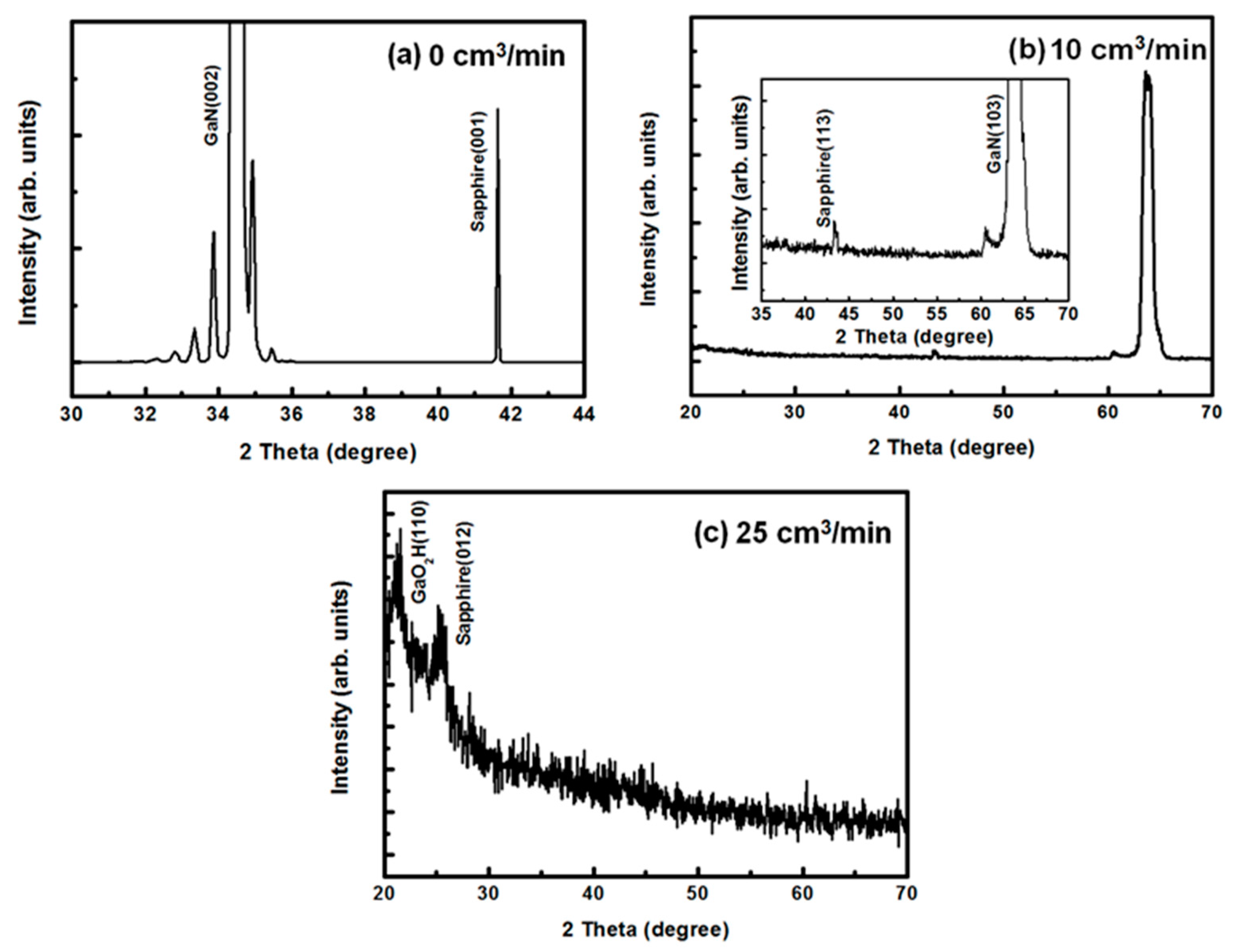
Figure 4 shows the XRD spectra of the GaN-epi/PSSs decomposed under gas flow rates of 0, 10, and 25 cm3/min. In the absence of H2 gas (0 cm3/min; Figure 4a), the XRD spectrum shows a GaN (002) peak located at approximately 2θ = 34.6° and several satellite peaks from InGaN/GaN multiple quantum well structures. The sapphire (001) phase near 41.6° also appears. Under the lower gas flow (10 cm3/min; Figure 4b), sapphire (113) and GaN (103) peaks are observed at approximately 43.4° and 63.6°, respectively. The GaN (103) peak is strong, but the GaN (002) peak and several satellite peaks have disappeared, indicating that the GaN film had gradually decomposed. Increasing the gas flow rate to 25 cm3/min completely removed the GaN phase, as shown in Figure 4c. The result implies that the GaN-epi/PSSs was completely decomposed under sufficiently high gas flow rates. These phenomena well agree with the results in Figure 2. Notably, in the grazing angle-XRD spectra under 25 cm3/min gas flow, the GaO2H (110) peak was located at 21.47°, indicating that GaO2H was present on the exposed PSS surface after the GaN had decomposed. In our previous study, the chemical reaction of the GaN decomposition was described as [18]
GaN(s) + H2(v) + 1/2 O2(v) + 1/4 N2(v) = 1/2 Ga(v) + 1/2 GaO2H(s) + 1/2 N2(v) + 1/2 NH3(v)
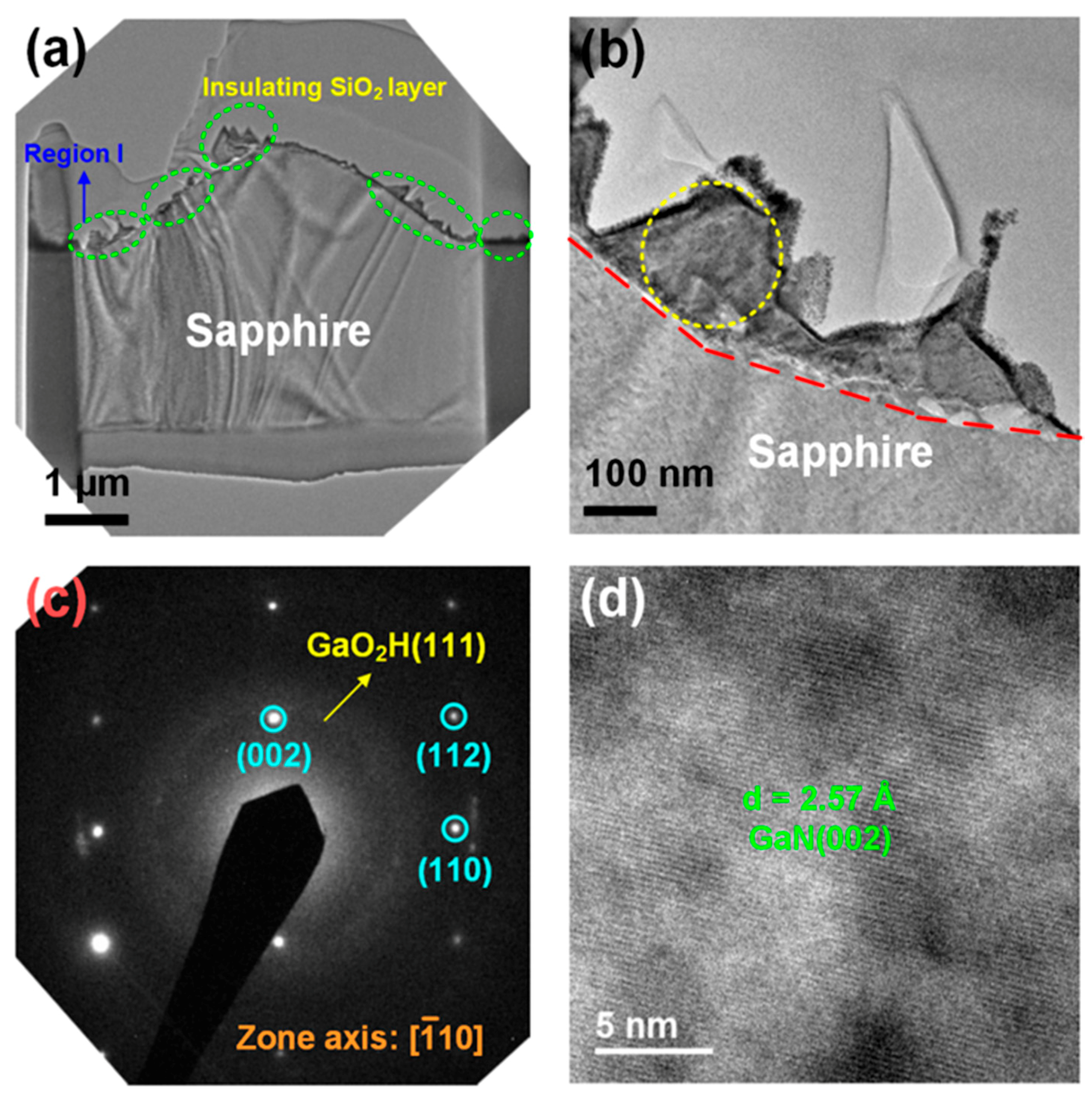
The microstructures of the GaN-epi/PSSs after decomposition were investigated by TEM. The samples prepared for decomposition at 1200 °C for 3 h under gas flows of 10 and 25 cm3/min were analysed sequentially. Figure 5a shows the cross-sectional TEM image of the GaN-epi/PSS sample decomposed under 10 cm3/min. Several residues (marked with green circles) appear on the bottom, sidewall, and top areas of the pattern. One of these residues (marked as region I) was selected for further observation. Moreover, the insulating SiO2 layer on these residues was deposited for the focused ion beam (FIB) process. Figure 5b is a higher-resolution TEM image of region I, which clarifies the interface between the region and the sapphire. Note that the residues were irregularly shaped. The selected area electron diffraction (SAED) pattern of region I (focused on the area delineated by the yellow circle in Figure 5b) is presented in Figure 5c. The regularly arranged diffraction dots reveal a single crystal structure of the residues. After analysis of this single-crystalline diffraction pattern, the residue was identified as GaN epilayer grown along the [002] direction (with the zone axis). A ring diffraction pattern with very weak intensity also appeared (Figure 5c). The ring pattern was indexed to the GaO2H (111) phase, suggesting that GaO2H nanocrystals were formed in the residue. Figure 5d is a high resolution TEM (HR-TEM) image of the area enclosed by the yellow circle in Figure 5b. The image shows a regular lattice arrangement. The d-spacing was determined as 2.57 Å and was identified as the GaN (002) plane. Obviously, even at the lower gas flow rate (10 cm3/min), GaN residues existed on the PSS. Based on the above-phenomenon, the GaN was only partially decomposed under gas flows of 10 cm3/min, and the small amount of GaO2H was formed on the GaN surface of the incompletely decomposed. Consequently, none of the GaO2H phases were detected by XRD (see Figure 4b).
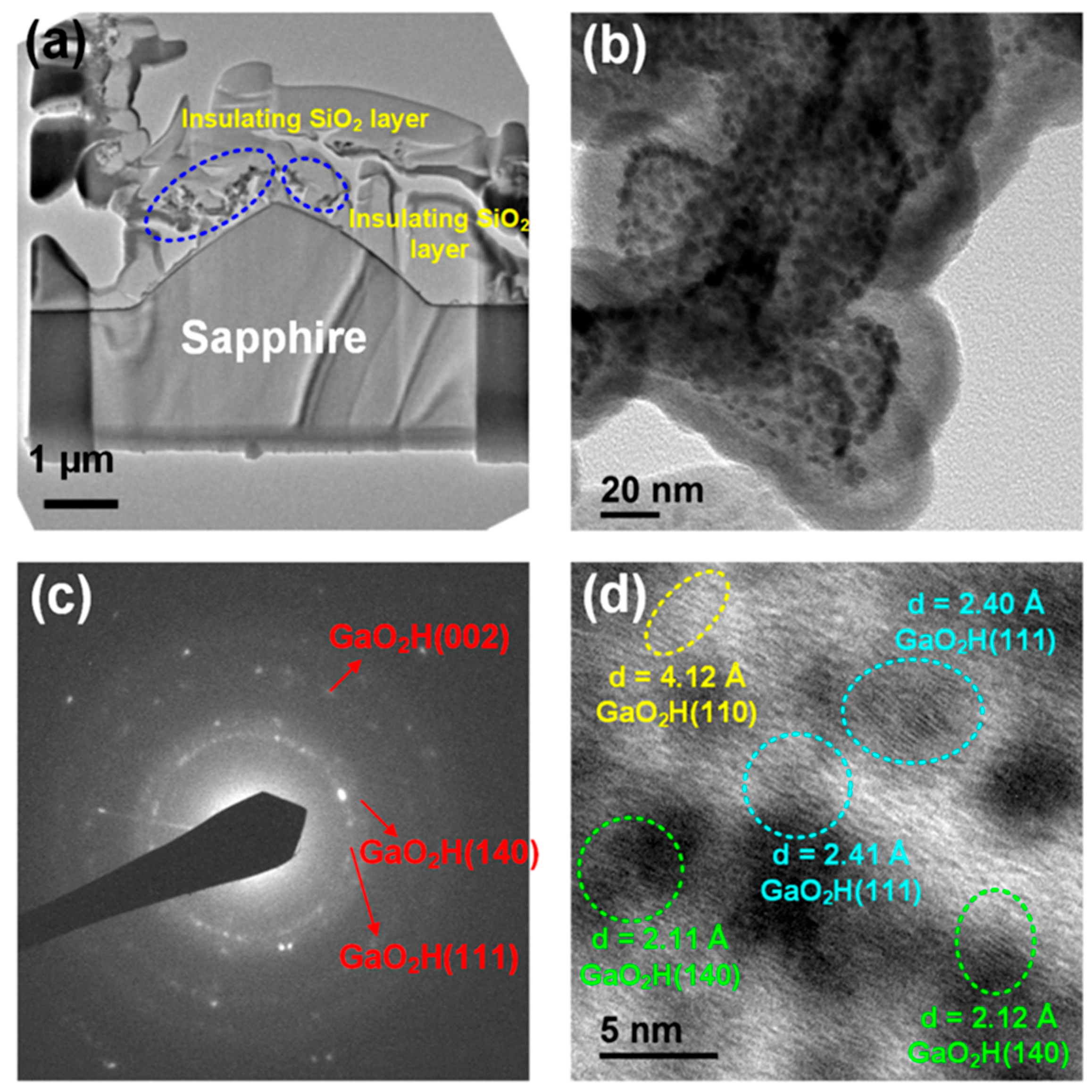
Figure 6 displays the TEM results of the GaN-epi/PSSs sample decomposed at 1200 °C under the high gas flow rate (25 cm3/min). As shown in the cross-sectional TEM image (Figure 6a), there was less residue on this sample than on the sample decomposed under the 10 cm3/min flow (Figure 5a). The insulating SiO2 layer also can be found in Figure 6a. Moreover, several nanostructures were formed during the decomposition process (marked with blue circles in the image). The morphology of the nanostructures can be observed in the plane-view SEM image (Figure 1f). The same nanostructures were found in the sample decomposed under the 10 cm3/min flow. During the FIB process, the nanostructures were easily broken and disappeared from the surface. Thus, almost no nanostructure is visible in Figure 5. To understand the formation of these nanostructures, we observed them under a higher TEM magnification (Figure 6b). Interestingly, these nanostructures were aggregates of many nanograins of size 2–5 nm. Figure 6c shows the SAED pattern of the nanostructures. The three diffraction rings were indexed to GaO2H (111), GaO2H (140), and GaO2H (002) phases. All rings were of very low brightness, indicating the poor crystal quality of the phases. Consequently, none of these phases were detected by XRD (see Figure 4). Although the GaO2H (110) diffraction peak appeared in the XRD pattern of Figure 4, no GaO2H (110) electron diffraction ring is visible in Figure 6c. We expected that the GaO2H (110) ring was close to the centre of the electron diffraction pattern, and was obscured by the very bright electron beam. Figure 6d is an HR-TEM image of the nanostructures. Several nano grains with various d-spacings were identified as GaO2H (110), GaO2H (111), and GaO2H (140) phases, again confirming that GaO2H (110) phase formed in the decomposed sample. A substrate can be completely reclaimed by removing the GaO2H reactant in alkaline solution [18].
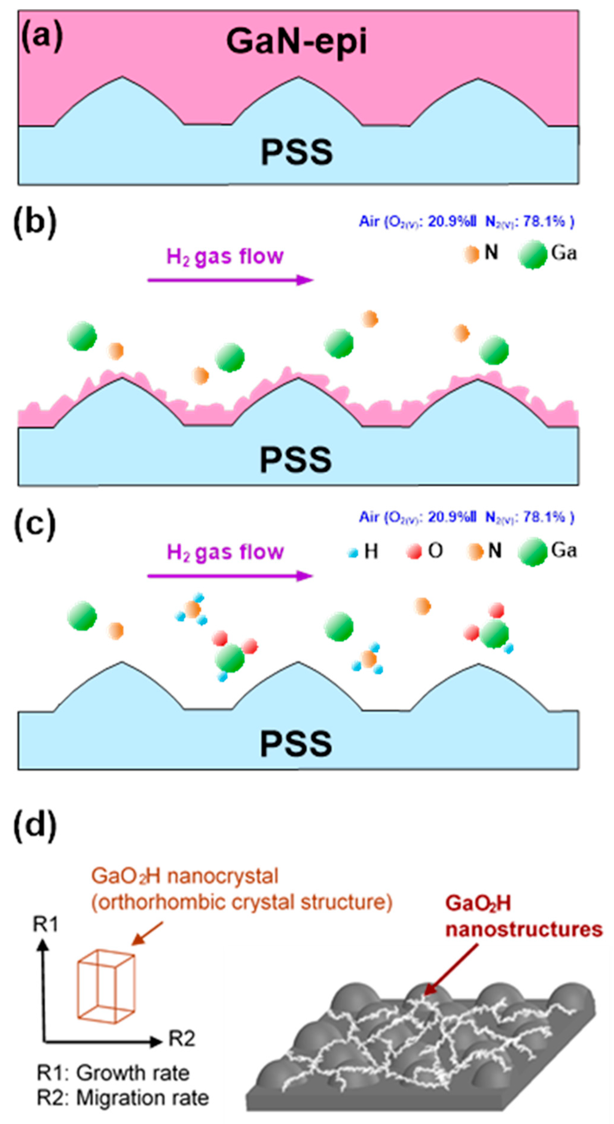
The behavior of GaN-based thermal decomposition in the hydrogen atmosphere is shown in Figure 7. When the GaN-epi/PSS sample was treated with hydrogen at high temperature (1200 °C), the hydrogen molecules began diffusing and adsorbing onto the GaN surface. Once adsorbed, they chemically reacted with GaN, releasing nitrogen atoms from the surface and leaving the Ga atoms. This mechanism is schematized in Figure 7a,b. Some of the Ga atoms reacted chemically with the O atoms in the air and the loading gas H2, forming GaO2H nanocrystals. Meanwhile, some of the N atoms reacted with H2 to produce NH3. The NH3 byproduct and the unreacted gas molecules (Ga, N2, and the loading gas H2) were expelled from the reaction chamber by forced convection, leaving only the GaO2H nanocrystals (Figure 7c). The remaining GaO2H nanocrystals were formed a discontinuous and uneven GaO2H nanostructure on the exposed PSS surface (see Figure 7d). This behavior was attributed to the smaller grains sized, the lower surface growth rate than migration rate of the GaO2H nanocrystals, and the surface migration distance lengthens at the high temperature. It is worth mentioning that the crystal structure of the InGaN well layers was a small amount of In doped to GaN and only partially replaced the crystal position of Ga. Therefore, the behavior of the InGaN thermal decomposition in the H2 atmosphere was similar to that of the GaN thermal decomposition. The H2 chemically reacted with InGaN, releasing nitrogen atoms and leaving the In and Ga atoms, and the unreacted In and Ga gas molecules were expelled from the reaction chamber.
4. Conclusions
We completely decomposed GaN under a hydrogen atmosphere, and discussed the decomposition mechanism. Hydrogen promoted the decomposition of GaN into Ga and N atoms; the Ga atoms then reacted with oxygen in the atmosphere and the hydrogen loading gas to form GaO2H nanocrystals. Interestingly, these GaO2H nanocrystals formed a discontinuous and uneven GaO2H nanostructure on the exposed PSS surface. This behavior was attributed to the smaller grains size, the lower surface-growth rate than migration rate of the GaO2H nanocrystals, and the surface migration distance lengthens at the high temperature. A complete substrate reclamation process is possible by removing the GaO2H reactant using alkaline solution. The decomposition mechanism is potentially applicable to the reclamation of sapphire substrates in the GaN-based semiconductor industry.
Author Contributions
Conceptualization, S.-Y.H.; methodology, S.-Y.H.; data curation, J.-C.L., S.-L.O. and S.-Y.H.; writing—original draft preparation, S.-L.O. and S.-Y.H.; writing—review and editing, S.-Y.H.; supervision, S.-Y.H.; project administration, S.-Y.H.
Funding
This research was funded by the National Science Council (NSC) and the Ministry of Science and Technology (MOST), Taiwan, under Contract Nos. NSC 101-2218-E-212 -001, and MOST 107-2221-E-212-008, respectively.
Conflicts of Interest
The authors declare no conflict of interest.
References
- Steigerwald, D.A.; Bhat, J.C.; Collins, D.; Fletcher, R.M.; Holcomb, M.O.; Ludowise, M.J.; Martin, P.S.; Rudaz, S.L. Illumination with solid state lighting technology. IEEE J. Select. Top. Quantum Electron. 2002, 8, 310–320. [Google Scholar] [CrossRef]
- Colombo, L.; Dolara, A.; Guzzetti, S.; Lazaroiu, G.C.; Leva, S.; Lucchini, A. Thermal and luminous investigations of a pc LED based refrigerating liquid prototype. Appl. Therm. Eng. 2014, 70, 884–891. [Google Scholar] [CrossRef]
- Cheng, H.; Lin, J.; Chen, W. On the thermal characterization of an RGB LED based white light module. Appl. Therm. Eng. 2012, 38, 105–116. [Google Scholar] [CrossRef]
- Jiang, H.; Egawa, T. High quality AlGaN solar-blind Schottky photodiodes fabricated on AIN/sapphire template. Appl. Phys. Lett. 2007, 90, 121121. [Google Scholar] [CrossRef]
- Srour, H.; Salvestrini, J.P.; Ahaitouf, A.; Gautier, S.; Moudakir, T.; Assouar, B.; Abarkan, M.; Hamady, S.; Ougazzaden, A. Solar blind metal-semiconductor-metal ultraviolet photodetectors using quasi-alloy of BGaN/GaN superlattices. Appl. Phys. Lett. 2011, 99, 221101. [Google Scholar] [CrossRef] [Green Version]
- Cherkashinin, G.; Lebedev, V.; Wagner, R.; Cimalla, I.; Ambacher, O. The performance of AlGaN solar blind UV photodetectors: Responsivity and decay time. Phys. Status Solidi B 2006, 243, 1713–1717. [Google Scholar] [CrossRef]
- Munir, Z.A.; Searcy, A.W. Activation energy for the sublimation of gallium nitride. J. Chem. Phys. 1965, 42, 4223. [Google Scholar] [CrossRef]
- Thurmond, C.D.; Logan, R.A. The equilibrium pressure of N2 over GaN. J. Electrochem. Soc. 1972, 119, 622–626. [Google Scholar] [CrossRef]
- Logan, R.A.; Thurmond, C.D. Heteroepitaxial thermal gradient solution growth of GaN. J. Electrochem. Soc. 1972, 119, 1727–1735. [Google Scholar] [CrossRef]
- Koleske, D.D.; Wickenden, A.E.; Henry, R.L.; Culbertson, J.C.; Twigg, M.E. GaN decomposition in H2 and N2 at MOVPE temperatures and pressures. J. Cryst. Growth 2001, 223, 466–483. [Google Scholar] [CrossRef]
- Mastro, M.A.; Kryliouk, O.M.; Reed, M.D.; Anderson, T.J.; Davydov, A.; Shapiro, A. Thermal stability of MOCVD and HVPE GaN layers in H2, HCl, NH3 and N2. Phys. Status Solidi A 2001, 188, 467–471. [Google Scholar] [CrossRef]
- Unland, J.; Onderka, B.; Davydov, A.; Fetzer, R.S. Thermodynamics and phase stability in the Ga–N system. J. Cryst. Growth 2003, 256, 33–51. [Google Scholar] [CrossRef]
- Mastro, M.A.; Kryliouk, O.M.; Anderson, T.J.; Davydov, A.; Shapiro, A. Influence of polarity on GaN thermal stability. J. Cryst. Growth 2005, 274, 38–46. [Google Scholar] [CrossRef]
- Peshek, T.J.; Angus, J.C.; Kash, K. Thermodynamic properties of gallium nitride. J. Cryst. Growth 2011, 322, 114–116. [Google Scholar] [CrossRef]
- Fahle, D.; Kruecken, T.; Dauelsberg, M.; Kalisch, H.; Heuken, M.; Vescan, A. In-situ decomposition and etching of AlN and GaN in the presence of HCl. J. Cryst. Growth 2014, 393, 89–92. [Google Scholar] [CrossRef]
- Bouazizi, H.; Chaaben, N.; Gmili, Y.E.; Bchetnia, A.; Salvestrini, J.P.; Jani, B.E. Study of the partial decomposition of GaN layers grown by MOVPE with different coalescence degree. J. Cryst. Growth 2016, 434, 72–76. [Google Scholar] [CrossRef]
- Bouazizia, H.; Bouzidia, M.; Chaaben, N.; Gmili, Y.E.; Salvestrini, J.P.; Bchetnia, A. Observation of the early stages of GaN thermal decomposition at 1200 °C under N2. Mater. Sci. Eng. B 2018, 227, 16–21. [Google Scholar]
- Huang, S.Y. Development of reclaimed pattern sapphire substrates technologies for GaN-based LEDs. ECS Trans. 2013, 53, 203–210. [Google Scholar] [CrossRef]
Figure 1.
Cross-sectional and plane-view SEM images of the GaN-based epilayers on patterned sapphire substrates (GaN-epi/PSSs) morphologies under H2 gas flowing at (a,b) 0 cm3/min, (c,d) 10 cm3/min, and (e,f) 25 cm3/min at 1200 °C for 3 h. The enlargement enclosed by the pink frame in panel (a) depicts a clear GaN-epi/PSS structure.

Figure 2.
Scanning electron microscopy–energy dispersive spectrometer (SEM–EDS) spectra of the GaN-epi/PSSs decomposed at 1200 °C for 3 h under hydrogen flow rates of (a) 0 cm3/min, (b) 10 cm3/min, and (c) 25 cm3/min.
Figure 2.
Scanning electron microscopy–energy dispersive spectrometer (SEM–EDS) spectra of the GaN-epi/PSSs decomposed at 1200 °C for 3 h under hydrogen flow rates of (a) 0 cm3/min, (b) 10 cm3/min, and (c) 25 cm3/min.

Figure 3.
Quantitative SEM–EDS results of the GaN-epi/PSSs decomposed at 1200 °C for 3 h under hydrogen flow rates of 0, 10, and 25 cm3/min.
Figure 3.
Quantitative SEM–EDS results of the GaN-epi/PSSs decomposed at 1200 °C for 3 h under hydrogen flow rates of 0, 10, and 25 cm3/min.

Figure 4.
XRD spectra of the GaN-epi/PSSs decomposed at 1200 °C for 3 h under gas-flow rates of (a) 0 cm3/min, (b) 10 cm3/min, and (c) 25 cm3/min.
Figure 4.
XRD spectra of the GaN-epi/PSSs decomposed at 1200 °C for 3 h under gas-flow rates of (a) 0 cm3/min, (b) 10 cm3/min, and (c) 25 cm3/min.

Figure 5.
(a) Cross-sectional transmission electron microscopy (TEM) image of the GaN-epi/PSS sample decomposed at 1200 °C for 3 h under a gas-flow rate of 10 cm3/min; (b) TEM image of region I taken at higher magnification; and (c,d) SAED pattern of region I and an high resolution transmission electron microscopy (HR–TEM) image, respectively, focused on the yellow-circled area in (b).

Figure 6.
(a) Cross-sectional TEM image of the GaN-epi/PSS sample decomposed at 1200 °C for 3 h under a gas-flow rate of 25 cm3/min; (b) TEM image of the nanostructures taken at higher magnification; and (c,d) SAED pattern and an HR–TEM image of the nanostructures, respectively.
Figure 6.
(a) Cross-sectional TEM image of the GaN-epi/PSS sample decomposed at 1200 °C for 3 h under a gas-flow rate of 25 cm3/min; (b) TEM image of the nanostructures taken at higher magnification; and (c,d) SAED pattern and an HR–TEM image of the nanostructures, respectively.

Figure 7.
Schematic diagram for (a) a GaN-epi/PSS structure, (b) the H2 chemically reacted with GaN, releasing nitrogen atoms and leaving the Ga atoms, (c) Some of the Ga atoms reacted chemically with the O atoms in the air and the loading gas H2, forming GaO2H nanocrystals. Meanwhile, some of the N atoms reacted with H2 to produce NH3, and (d) the remaining GaO2H nanocrystals were formed a discontinuous and uneven GaO2H nanostructure on the exposed PSS surface.


Table 1.
Compositions of the GaN-epi/PSSs under different gas flow rates, obtained by EDS.
| Gas-Flow Rates (cm3/min) | 0 | 10 | 25 |
|---|---|---|---|
| (wt.%) | (wt.%) | (wt.%) | |
| Ga atom | 71.13 | 5.56 | 0.12 |
| N atom | 20.43 | 2.14 | 0 |
| Al atom | 0 | 38.81 | 45 |
| O atom | 0 | 46.33 | 49.67 |
| C atom | 8.18 | 7.16 | 6.8 |
© 2018 by the authors. Licensee MDPI, Basel, Switzerland. This article is an open access article distributed under the terms and conditions of the Creative Commons Attribution (CC BY) license (http://creativecommons.org/licenses/by/4.0/).
Share and Cite
MDPI and ACS Style
Huang, S.-Y.; Lin, J.-C.; Ou, S.-L. Study of GaN-Based Thermal Decomposition in Hydrogen Atmospheres for Substrate-Reclamation Processing. Materials 2018, 11, 2082. https://doi.org/10.3390/ma11112082
AMA Style
Huang S-Y, Lin J-C, Ou S-L. Study of GaN-Based Thermal Decomposition in Hydrogen Atmospheres for Substrate-Reclamation Processing. Materials. 2018; 11(11):2082. https://doi.org/10.3390/ma11112082
Chicago/Turabian StyleHuang, Shih-Yung, Jian-Cheng Lin, and Sin-Liang Ou. 2018. "Study of GaN-Based Thermal Decomposition in Hydrogen Atmospheres for Substrate-Reclamation Processing" Materials 11, no. 11: 2082. https://doi.org/10.3390/ma11112082
Note that from the first issue of 2016, this journal uses article numbers instead of page numbers. See further details here.