
A 0.5 V Sub-Threshold CMOS Current-Controlled Ring Oscillator for IoT and Implantable Devices


1
Dipartimento di Ingegneria Elettrica Elettronica e Informatica (DIEEI), University of Catania, 95125 Catania, Italy
2
Dipartimento di Ingegneria dell’Informazione Elettronica e Telecomunicazioni (DIET), Sapienza University of Rome, 00184 Rome, Italy
*
Author to whom correspondence should be addressed.
J. Low Power Electron. Appl. 2022, 12(1), 16; https://doi.org/10.3390/jlpea12010016
Submission received: 8 February 2022
/
Revised: 24 February 2022
/
Accepted: 3 March 2022
/
Published: 9 March 2022
(This article belongs to the Special Issue Ultra-Low-Power ICs for the Internet of Things)
Abstract
:A current-controlled CMOS ring oscillator topology, which exploits the bulk voltages of the inverter stages as control terminals to tune the oscillation frequency, is proposed and analyzed. The solution can be adopted in sub-1 V applications, as it exploits MOSFETS in the subthreshold regime. Oscillators made up of 3, 5, and 7 stages designed in a standard 28-nm technology and supplied by 0.5 V, were simulated. By exploiting a programmable capacitor array, it allows a very large range of oscillation frequencies to be set, from 1 MHz to about 1 GHz, with a limited current consumption. Considering, for example, the five-stage topology, a nominal oscillation frequency of 516 MHz is obtained with an average power dissipation of about 29 µW. The solution provides a tuneable oscillation frequency, which can be adjusted from 360 to 640 MHz by controlling the bias current with a sensitivity of 0.43 MHz/nA.
1. Introduction
The Internet of Things (IoT), wireless sensor networks, and the emergence of other energy-harvested microsystems pose continuous challenges and create ever-growing interest in CMOS ultra-low-power analog and mixed-signal system-on-chip solutions. In this framework, applications such as wearable and implantable medical devices, body sensor networks, etc., often require a controlled oscillator (CO) with a minimum power consumption, small layout area, low phase noise, and adequate frequency tuning range to cope with process and/or temperature variations [1,2,3,4,5,6]. COs are also fundamental blocks of phase-locked loops (PLLs) to provide the timing basis in clock control, clock generator circuits, RFID tags, and systems that use clock-dependent circuits, such as switching power converters and so on [7,8,9].
CMOS COs can be categorized in two main families. The first includes LC resonant oscillators and, the second, ring oscillators. LC oscillators are mainly used in applications where both a high-phase noise and quality factor (Q) are required. Due to their spiral inductors’ large area and high-power dissipation, they cannot be used in ultra-low-power systems on a chip and where physical dimensions must be limited [10]. As is well known, ring oscillators (ROs) consist of an odd number of cascaded delay elements, usually identical to each other, that form a ring where the last stage output is connected to the first stage input. A further categorization is performed based on the control variable, which is often a voltage or a current.
Controlled ring oscillator topologies exhibit a good frequency tuning range, low power dissipation, low design complexity, occupy a small area, and compatibility with CMOS processes. Moreover, ring oscillators are more power efficient compared to relaxation oscillators, although these can achieve a wider tuning range [11].
To improve the frequency-tuning range and phase-noise margin, several design approaches for low-power COs have been reported in the literature. Among these techniques, we mention the combined current-starving technique (i.e., current-controlled oscillator) with a negative skewed-delay approach to improve the power delay product (i.e., product between dissipated power and single gate delay) [12]. A conventional voltage controlled oscillator (VCO) with a negative resistance, multiple-gated circuit and bypass capacitor to suppress high-order harmonics has been reported [13], whereas a digital control circuit to manage oscillation frequency has also been described [1]. An approach that uses positive feedback in each stage to operate with only two stages, instead of three, decreasing the power consumption can be found [14], whereas a frequency tuning cell that consists of one NMOS and one PMOS to form a transmission gate, used to tune the oscillation frequency by varying the gate voltage, has been presented [15]. Finally a dynamic threshold technique (DTMOS) to reduce the threshold voltage of NMOS transistors in the inverting stage with the aim to achieve fast transition and high operating frequency has been presented [3].
The idea of exploiting the bulk terminal to control the oscillation frequency of a RO and the effect of bulk voltage variations on RO phase noise have been analyzed [16], whereas an adaptive body-bias generator for low voltage CMOS VLSI circuits in which a RO was used to estimate the delay of CMOS gates has also been presented [17].
In this work, we exploit a body-biasing technique, originally utilized in the analog domain [18,19,20], and recently applied to set the quiescent current of the generic inverter stage [21] to design a low-power low-voltage current-controlled ring oscillator (CCO) in 28-nm bulk CMOS technology.
The proposed approach allows to guarantee a static output voltage equal to half the supply voltage, in spite of the value of the bias current, which is tuned in order to control the oscillation frequency. In this way, since any offset in the input output voltage transfer characteristic is removed by the body bias loop, the inverter stages can be reliably cascaded, thus greatly enhancing the tuning range and robustness to PVT variations of the proposed RO.
2. The Proposed Solution
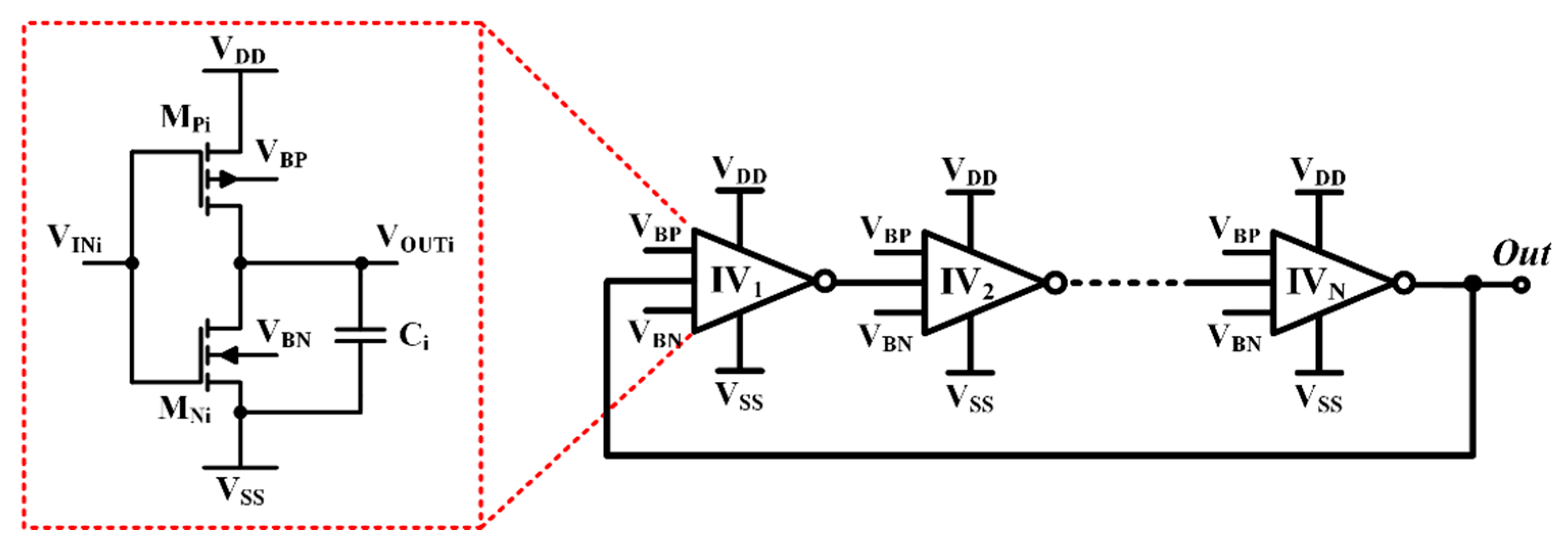
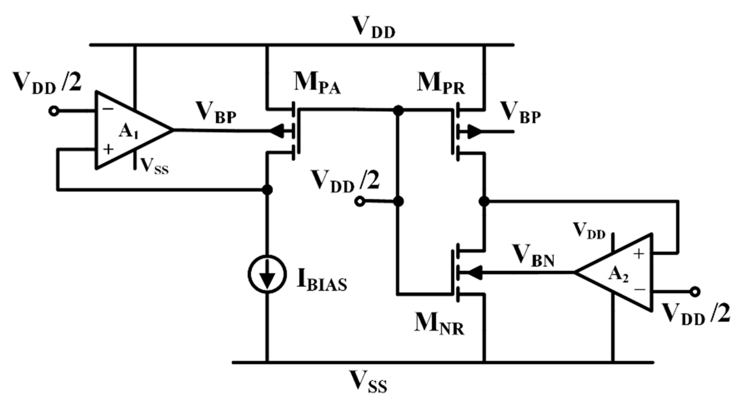
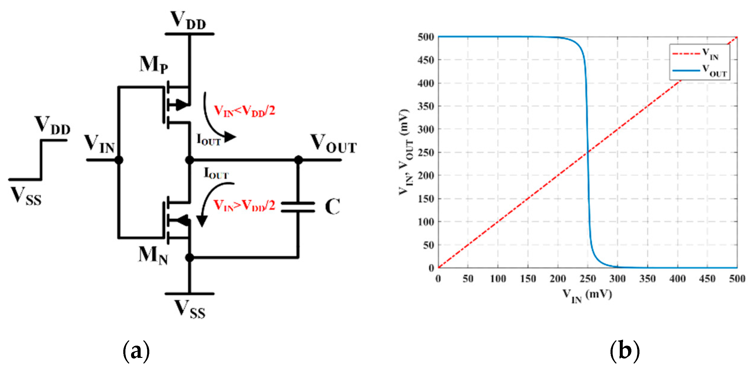
Figure 1 shows a circuit schematic of the proposed current-controlled ring oscillator (CCRO). It consists of an N-stage ring oscillator in which the single stage is made up of a CMOS inverter where bulk terminals of both transistors (MPi and MNi, with i = 1, 2, … N and N an odd number greater than 3) are made accessible. An output capacitor, Ci in the red-dashed box, is added at the output of each stage with the aim of setting the nominal oscillation frequency (coarse tuning), and to locally make the single stage insensible to parasitic capacitances, as will be clarified in the next section. The body potentials of both transistors, VBP and VBN, are generated from the auxiliary topology depicted in Figure 2, the aim of which is to establish the maximum current flowing in the reference inverter (MPR-MNR), i.e., when the input is at the logic threshold, VDD/2. For this purpose, in quiescent conditions, the input terminal of this reference inverter is set to VDD/2 and, thanks to the overall negative feedback implemented by error amplifier A2, such condition is transferred also to the output. Note that also the drain voltage of transistor MPA is kept to VDD/2 thanks to A1. This allows us to set the same nominal operating points for both MPR and MPA.
As far as the quiescent current control is concerned, it is implemented through the bulk terminals via voltage VBP for the p-channel transistors, and VBN for the n-channel ones. These voltages are generated by A1 and A2, exploiting a technique proposed in [19] and utilized also in [21].
In brief, starting from the biasing current IBIAS, transistor MPA is forced to generate voltage VBP, which is also applied to MPR. Therefore, current IBIAS in MPA is mirrored by transistor MPR that, as already stated, together with MNR, constitutes the reference inverter. Note also that A2 generates the required bulk voltages, VBN, for MNR to drive the same current of MPR under the constraints listed in the following:
- (a)
- assigned aspect ratios (W/L)PA, (W/L)PR and (W/L)NR;
- (b)
- ID,PR/NR = kIBIAS, where k = (W/L)PR/(W/L)PA;
- (c)
- VSG,PR = VGS,NR = VDD/2;
- (d)
- VSD,PR = VDS,NR = VDD/2, assuming ideal input virtual short in A1 and A2.
Of course, aspect ratios of MPR and MNR must be set so that the required bulk voltages are within VDD and ground. Moreover, the mirroring error between the biasing branch and the reference one is reduced using a careful layout style.
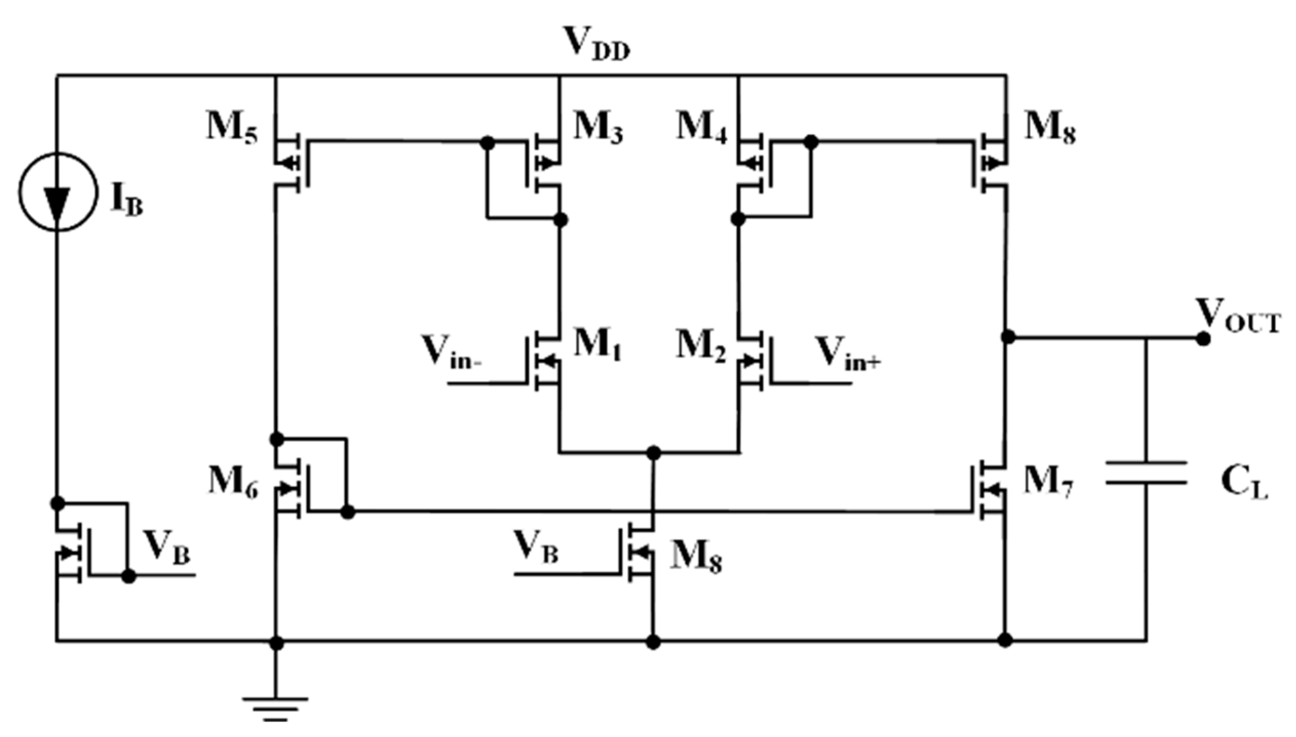
It should be noted that the auxiliary amplifiers A1 and A2 should provide a maximum (rail-to-rail) output voltage range, whereas input common mode range is not a concern as input voltage is kept constant to VDD/2. Therefore, simple symmetrical OTAs biased in subthreshold, can be effectively used. An example of implementation of this type of amplifier is found in [21,22], and is shown in Figure 3.
Voltages VBN and VBP are then applied to the inverters forming the ring oscillator in Figure 1, limiting at the desired value the maximum current flowing when the input voltage is equal to the threshold. Indeed, consider transistor MN1 of the first inverter stage, the exploded view of which is depicted in the red-dashed box in Figure 1. Let us remember that, in quiescent conditions, VIN1 is equal to VDD/2. Consequently, MNR and MN1 have respectively the same source, gate, and bulk voltage and hence the drain current of MN1 is related to that of MNR in a mirror-like condition:
where equality is accurately verified because the source-drain voltage of MN1 is also equal to VDD/2. Similar considerations hold for all the transistors in the ring oscillator, in practice, all p-channel and n-channel devices have their current linked to IBIAS via the current-mirror relations
where (W/L)Pi and (W/L)Ni, with i = 1, 2, … N, are, respectively, the aspect ratios of the generic p-channel and n-channel MOSFET in the ring oscillator.
3. Small- and Large-Signal Analysis of the Proposed Ring Oscillator
In order to design a conventional ring oscillator, analytical extraction of design equations is carried out by using two main approaches.
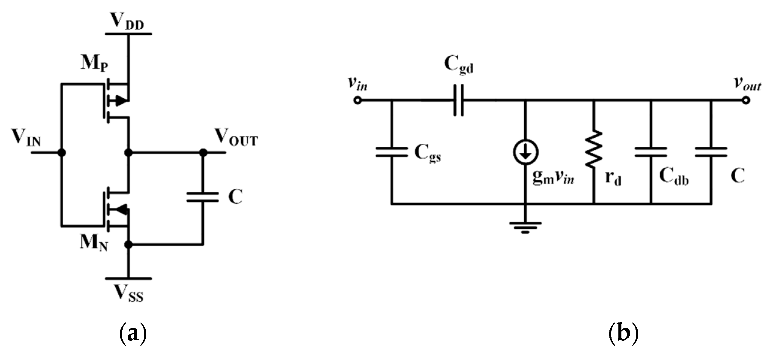
The first type of analysis considers small-signal equivalent model of the sub-blocks and Barkhausen stability criterion. In this approach the single gate is seen as working in an operating point (biasing or linearity conditions) and the whole system is analysed in the frequency domain. For this reason, hereinafter we will refer to this approach as an analog or small-signal approach. As an example, let us consider the conventional CMOS inverter in Figure 4 and its equivalent small-signal circuit.
When working around an operating point, the inverter behaves as the linear network reported on the right side of Figure 4, the parameters of which are expressed below for the MOS transistors operated in the sub-threshold region.
where parameter n is the sub-threshold slope, VT = kT/q is the thermal voltage, with k the Boltzmann constant, T is the absolute temperature and COX is the oxide capacitance for unit of area. In addition, λDS is the channel modulation coefficient, Lov is the length of the overlap portion, CJp/n is the capacitance of the S/D junctions (evaluated at the voltage VDD/2 in (4e)), mj is the grading coefficient and Vbi is the built-in voltage.
The product between the transconductance gm (4) and the output resistance rd (5) yields a constant value, independent of the biasing current ID and equal to the maximum of the gm/ID curves [23]. In such case, only the channel modulation coefficient, λDS/nVT, can be changed by sizing the transistors, in order to (slightly) change the inverter intrinsic gain (i.e., gmrd). Note that the drain-induced barrier lowering (DIBL) effect is included in the channel modulation coefficient through the parameter λDS. Parasitic capacitance contribution accounts for three capacitances expressed in (6)–(8).
The gate-to-source equivalent capacitance is proportional to COX and is constituted by a first term that depends on the MOSFET active areas and by the operating condition (assumed with MOSFETs in saturation) and a second term that depends on the overlap capacitance. A similar contribution forms the gate-to-drain equivalent capacitance, Cgd, expressed in (7). The drain-to-bulk capacitance, unlike the previous two, is a non-linear capacitance which depends on S/D diffused areas (included in CJp/n) and the applied voltage, i.e., the drain-to-bulk voltage. Referring to Figure 4a, both are evaluated in the quiescent point, i.e., at VDD/2, and, from Figure 4b, the output node results to be loaded by the sum of the capacitances (8) and the additional one, C.
The above derivation, when applied to the proposed circuit, yields the same equations except for (4e) that becomes:
However, the effect of Cdb on the oscillation frequency can be neglected if an additional capacitance, C, sufficiently large, is connected in parallel. Analysis of the complete ring oscillator leads to closed-loop gain and phase shift which satisfy Barkhausen’s criteria for the common pulsation, ωp, since the output node electrically coincides with the input one, therefore |H(jωp)| = 1, and the a total phase shift of 180° is constantly achieved for an odd number of stages N. The result of these concurrent conditions ensures oscillation whose frequency is expressed by:
Here ctot gathers all the capacitive contributions (6), (7) doubled for Miller’s effect, (9) and C. It can be noted that, being the output small-signal resistance inversely proportional to the biasing current, ID, a proportional control of the oscillation frequency can be operated by varying the current itself. Various works presented in literature demonstrated that such kind of analysis is inaccurate when the number of stages exceeds 3, hence (10) is rarely used to design a ring oscillator.
On the other hand, the second approach consider the oscillator as the cascade of an odd-number of digital inverting gates where the output of the last gate is fed-back to the input of the first one. In this framework, the single inverter is characterized by its propagation delay, τPD, and the frequency of the generated signal follows the expression:
where the factor 2 derives from the fact that each single voltage node switches N-times τPD, where N is the number of inverters involved. For a digital gate, the propagation delay is defined as the time required to settle the output node to the middle of its dynamic range as referred to the instant of input changing. Henceforth, we call this approach digital or large-signal approach. While the simple relation in (11) and its scalability assuming general gate implementation are the strengths of this approach, evaluating τPD could require a great deal of effort. Therefore, designers often adopt a trial-and-error approach.
To better understand the relation between small- and large-signal behavior, propagation delay of the proposed cell should be evaluated. Figure 5 shows the working principle of the inverting gate in response to an input rail-to-rail signal and its static behavior as well. Assuming the inverter symmetrical and working in sub-threshold, which means to size transistors aspect ratios meeting the relationship
where both IST0,N (IST0,P), defined as the potential sub-threshold current of the NMOS (PMOS) if the threshold voltage are nullified, and n are technology-dependent parameters, and VTH,N (VTH,P) are the threshold voltage of the involved transistors. In (12), the tailing effect of drain-to-source voltages is neglected because we assume that transistors are biased in saturation, i.e., VDD/2 > VT. Moreover, VTH,N (VTH,P) implicitly depends on VBS,N (VSB,P) through the body effect, as well as on VDS,N (VSD,P) through the DIBL effect. Their contributions are taken into account by expressing VTH,N = VTH0,N − λBS,N VBS,N − λDS,N VDS,N(|VTH,P| = |VTH0,P| − λBS,P VSB,P − λSD,P VSD,P) where VTH0,N (VTH0,P) and λBS,N (λBS,P) are two technology parameters, while λDS,N (λSD,P) coincides with that used in (5) [24]. It should be noted that, if (12) is fulfilled, the two transistors are equally strong, which means that for the same gate to source voltage they conduct the same current. Under the aforementioned considerations, a good approximation (typical error < 10%) for the propagation delay is given by [25]:
In the first expression of (13), almost all the technology-dependent characteristics and transistor sizes are gathered in IST|VDD = 0 in order to be enucleated from the circuital parameters like voltages VDD, VBN, and VBP. Moreover, the total large-signal capacitance seen at the output node, CTOT, can be assumed to be equal to the small-signal one reported in (10). Finally, (13) has be re-written in the last simple form to highlight the biasing current, ID.
Replacing (13) in (11), the oscillation frequency is expressed as:
As compared with the small-signal counterpart, (14), like (10), shows a linear dependence with the bias current, therefore confirming the possibility to modulate the oscillation frequency of the RO by using the biasing circuit in Figure 2. It should be noted that (14) and (10) give similar information also when the last one loses accuracy. In fact, for N > 3 the tangent function can be expanded in Taylor’s series, Tan(π/N) ≈ π/N being π/N << 1. This approximation leads to have:
which differs from (14) only for factor (λDS/nVT) that replaces (/VDD). Thus, it can be claimed that small-signal and large-signal analyses yield results that are similar to those obtained for a conventional topology, such as the current-starved RO [26].
In conclusion, three important metrics for a controlled oscillator are evaluated. Starting from (14), the first is the frequency-to-current first-order slope defined as the derivative function of the frequency versus the control current:
The second one is the total power consumption, made up of a static and a dynamic contribution. While the static part is due only to the leakage current, which coincides with the quiescent one in our case and, as it will be seen it is negligible; the dynamic part represents the major contribution to the power consumption. Consequently, the dynamic power dissipation PD of a N-stage ring oscillator is given by:
Finally, in a conventional CMOS oscillator, the amount of the phase noise, L{Δf}, (see expression (15) of [27]) is given by the flicker noise and its normalized single-sideband spectral density as given in the following equation
where Δf is the offset frequency from the nominal one fOSC, Q is the quality factor and F is an empirical fitting parameter that takes the increased noise in Δf into account. The Q factor is typically used in the design of high-order oscillators like LC-type and is defined as the ratio of the energy stored in the oscillating resonator to the energy dissipated per cycle by damping processes. Finally, Psign in (18) is the power of generated signal. Unfortunately, as in the conventional ring oscillator, the quality factor is poor since the energy stored in the node capacitances is reset(discharged) every cycle [27], resulting in a higher phase noise.
Finally, the trade-off between phase noise, power consumption and carrier frequency can be evaluated by using the following figure of merit (FoM):
where P(mW) is the power consumption expressed in mW, thus normalized to 1 mW.
4. Validation Results
The proposed solution in the version of 3-, 5- and 7-stage CROs was designed in a 28-nm triple-well CMOS technology provided by TSMC and simulated at the schematic level. To set symmetrical behavior of the inverter, of the control bulk voltages ranges and body effect coefficients, MOS transistors with different thresholds were exploited. Specifically, HVT (high threshold) n-channel with 515-mV VTH and SVT (standard threshold) p-channel devices with −460-mV VTH, were adopted. A single power supply of 0.5 V was set and IBIAS was 320 nA. Reference operating temperature was in the range from 0 °C to 60 °C, suitable for implanted and wearable circuits. Transistor dimensions, together with other component values, are summarized in Table 1.
All p-channel (n-channel) MOSFETS are equal to the reference device 8.28/0.18 (5.4/0.18) μm/μm, where channel length was slightly increased as respect to the minimum one (100 nm) to counteract the short-channel effect. With these design choices the mirroring coefficient, ki, and the ratios of the transistors’ form factors in (1)–(3) are all reduced to the unity. As a consequence of the transistor’s dimension, the nominal quiescent current in each branch, which coincides with its short-circuit current, of 320 nA, resulting in a total nominal quiescent current of N-times 320 nA. Coarse tuning capacitor Ci was set to 10 fF for all stages. The DC gain of the auxiliary amplifiers, A1 and A2, with transistors in subthreshold, was around 30 dB and the gain-bandwidth product was 10 kHz, while consuming only 50 nA.
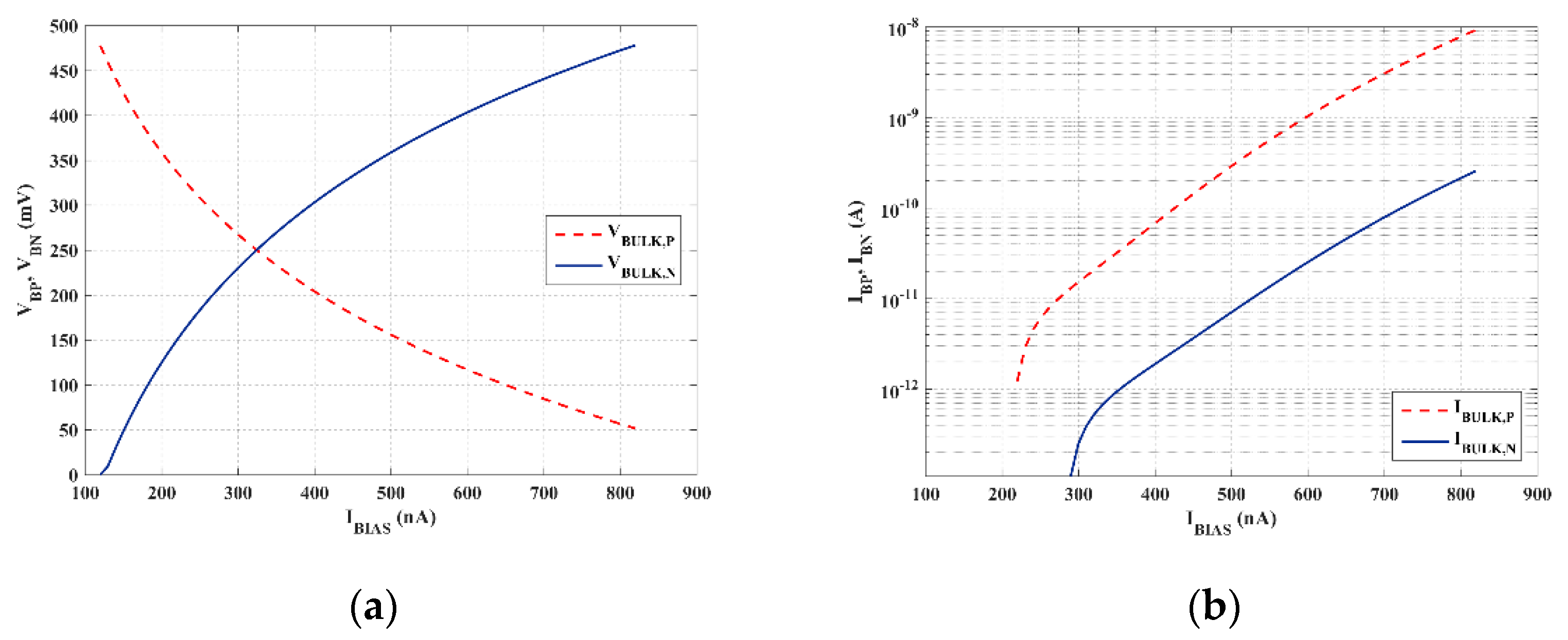
The robustness of the quiescent conditions was validated at first. The nominal bulk voltages, VBP and VBN, generated by the circuit in Figure 2 were 251 mV and 249 mV, respectively. The simulated quiescent current in the main ring oscillator in Figure 1 was 961, 1602 and 2243 nA on average, with a standard deviation of 48.5, 78.3, and 107 nA, respectively, for 3-, 5-, and 7-stage topology after running 1000 Monte Carlo iterations. The difference with respect to the expected values is mainly due to the low DC gains of the auxiliary amplifiers, which cause a closed-loop gain error.
Figure 6a shows the body voltages of the transistors involved in the reference inverting gate for a sweeping of the biasing current, IBIAS, in the range 120 nA–820 nA. The voltages fall within the supply rails and, in particular, it is easy to observe that their behaviors are symmetrical, confirming a good sizing of the block and the possibility to exploit the full dynamic range of the control voltages. Currents entering in the body terminals have been also evaluated and reported in Figure 6b to highlight that body junctions are never fully turned on during the control operation. In fact, the values of body currents in the worst case (PMOS), reach around 10 nA, corresponding to less than 2% of the biasing one.
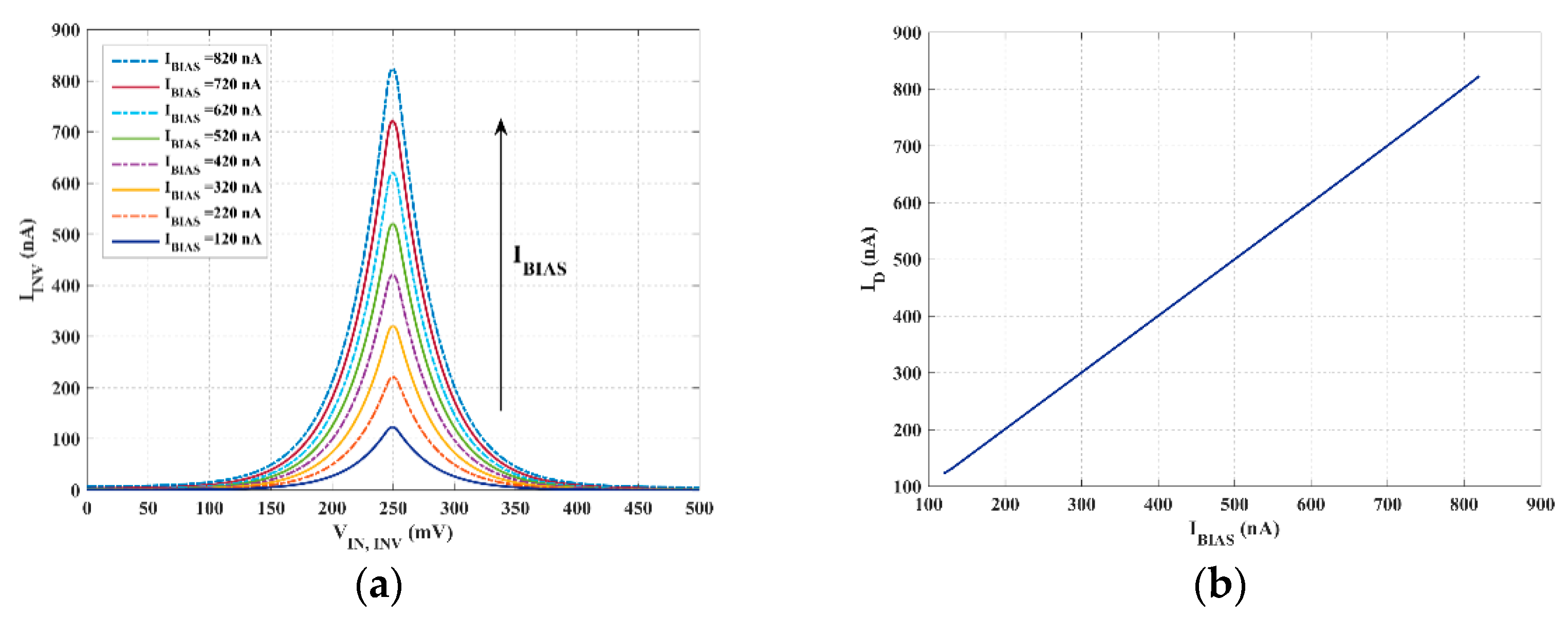
Figure 7a depicts the current flowing in the reference inverting gate when its input is varied from 0 to VDD (500 mV). As expected, the maximum is achieved for VDD/2 and accurately follows IBIAS as a validation of the effectiveness of the exploited biasing strategy and the linearity of the relation between the two quantities as well.
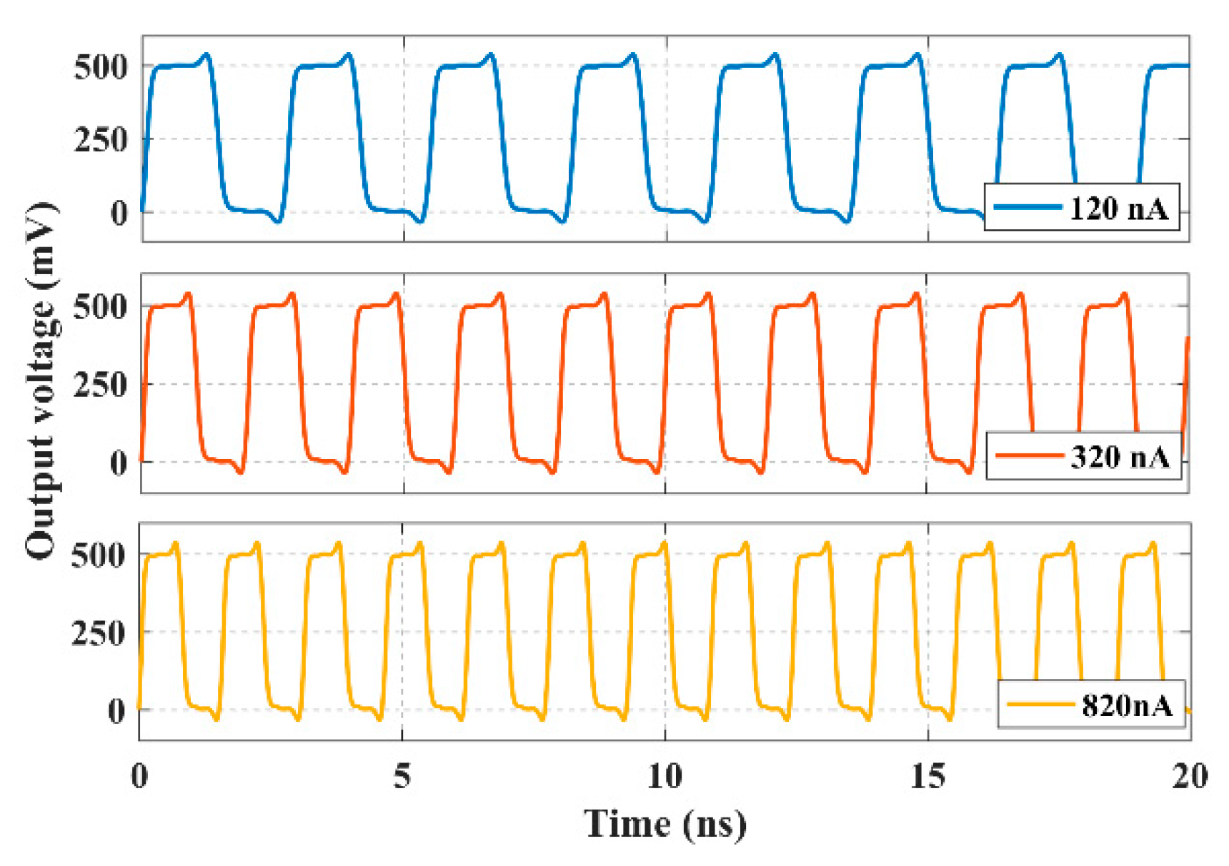
Figure 8 illustrates the output signal of the 5-stage CRO with Ci = 10 fF for three values of biasing current, 120, 320, and 820 nA, representing the minimum, nominal and maximum value, respectively.
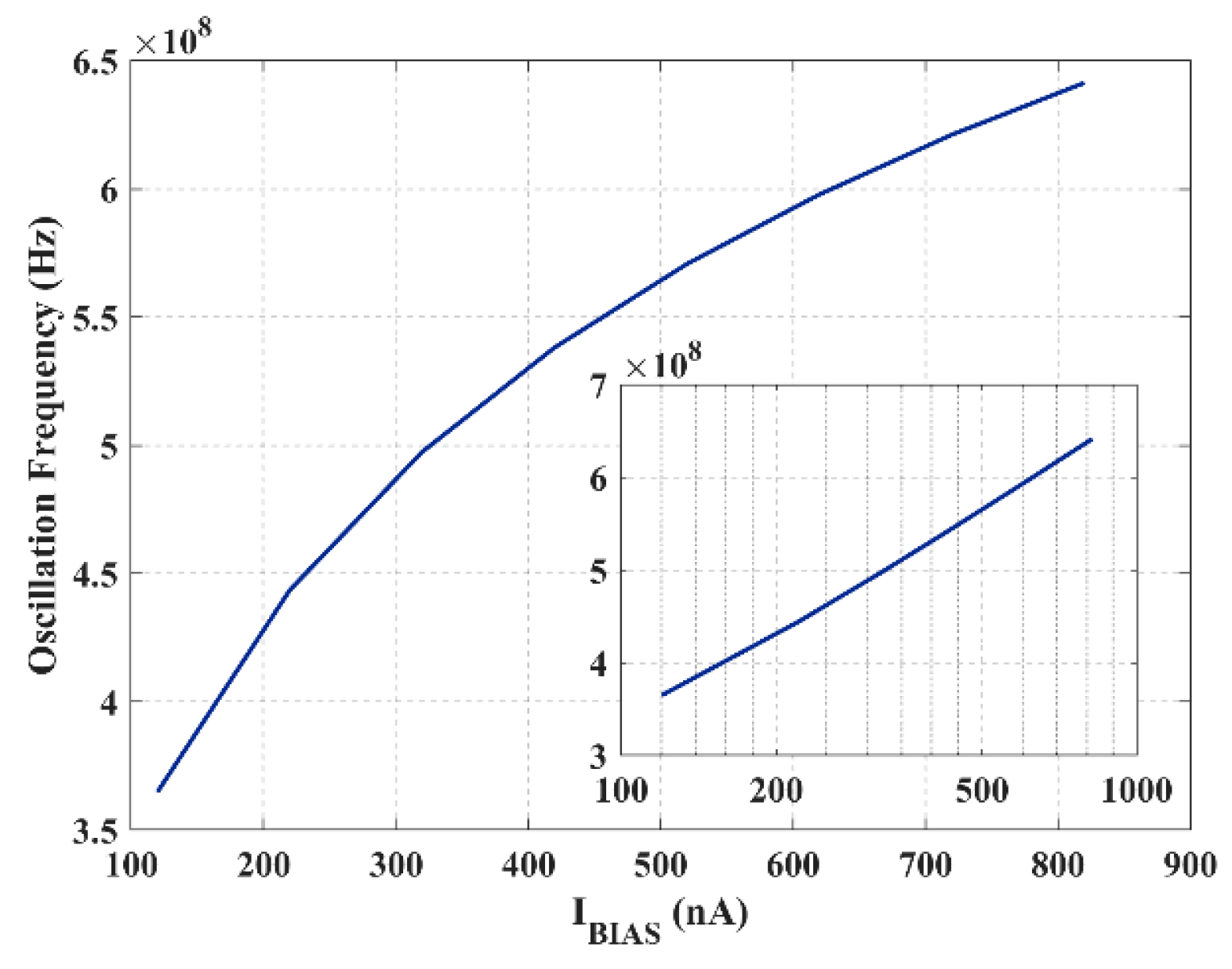
Figure 9 shows the oscillation frequency as a function of biasing current (Ci = 10 fF). An oscillation range from 360 MHz to 640 MHz is found with tuning sensitivity, i.e., the ratio between (fMAX − fMIN)/(IBIAS,MAX − IBIAS,MIN), about equal to 0.43 MHz/nA. Compared with the predicted behavior (linear relationships resulting from (14) and (15)), the obtained one shows a logarithmic relationship with IBIAS. This is confirmed by the inset plot in the same figure, the x-axis of which is logarithmic and slightly extended to cover an entire decade. Such changing in the behavior may be due to the partial operation in moderate inversion region, where subthreshold equations lose accuracy.
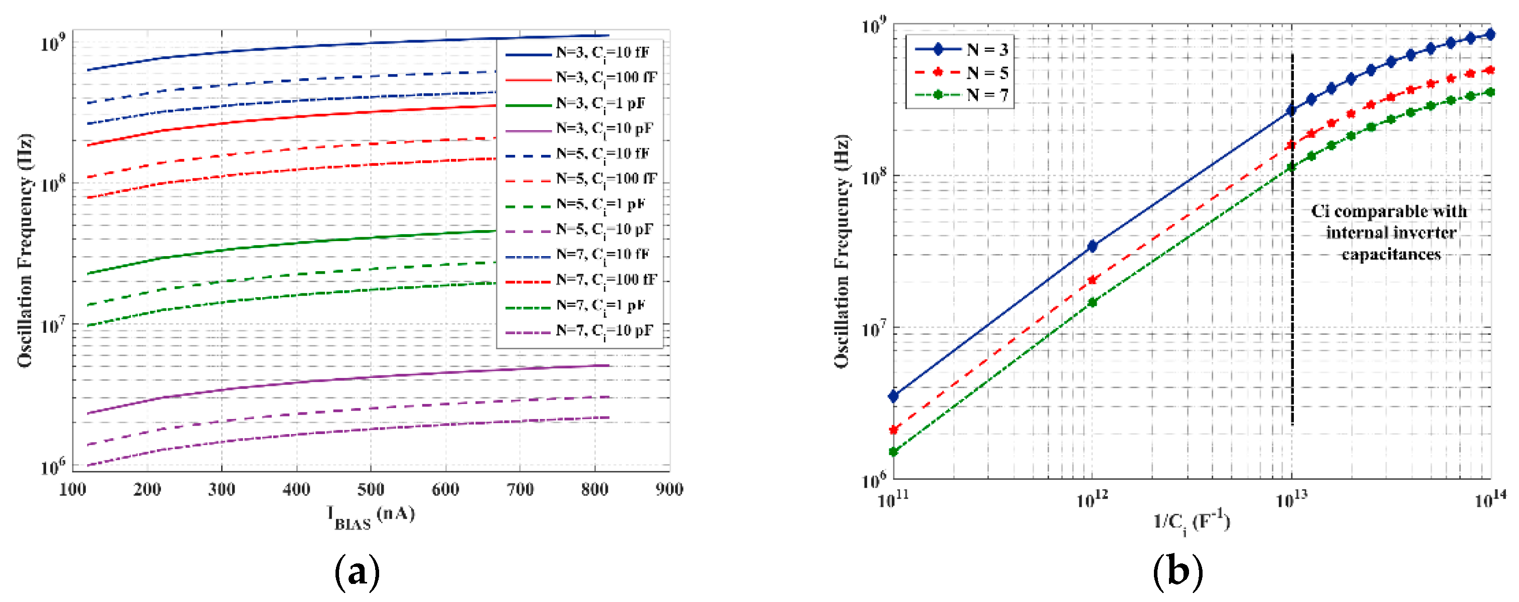
Figure 10a,b shows oscillation frequency with number of stages N equal to 3, 5, and 7 and for different coarse tuning capacitances, Ci, in the considered current biasing range (Figure 10a) and for a fixed IBIAS = 320 nA (Figure 10b) at T = 30 °C. It is apparent that frequency varies with the bias current, independently of the number of stages and coarse tuning capacitance. Constant spacing between two adjacent curves shows that the number of stages N acts as a scaling constant factor in the expression of the frequency, as predicted by (14) or, equivalently, (15). Moreover, Figure 10b highlights that the coarse tuning capacitance is comparable, in the range between 10 fF and 100 fF, with the parasitic inverter capacitances, being the oscillation frequency to capacitance relation compressed in this range.
Figure 9 and Figure 10 also show that the proposed solution may be used in an automatic design procedure, which, starting from the oscillation frequency specification and the nominal bias current, allows to determine the number of inverter stages (which can be taken from a standard-cell library providing access to the bulk terminals) and the coarse tuning capacitances (which can be taken from a capacitor array). The bias current is then used to perform oscillation frequency tuning to counteract process and temperature variation effects.
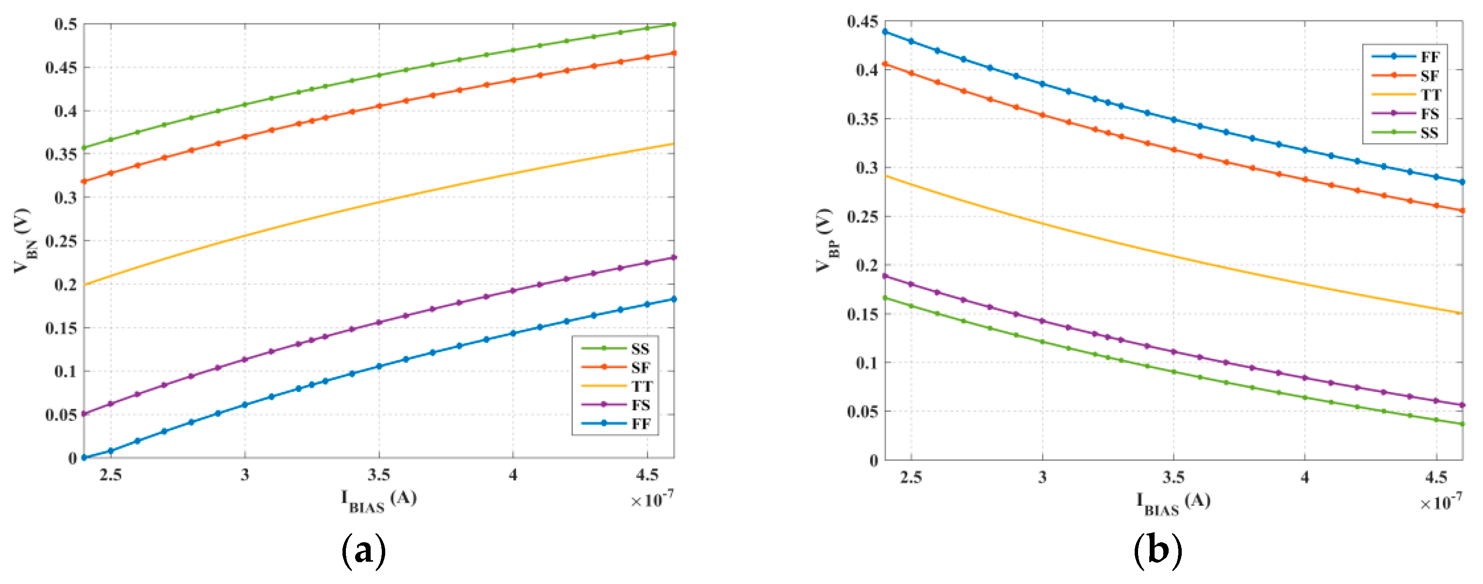
At this purpose, corner analyses were carried out for the 5-stage topology as an illustrative example. Figure 11 shows the two bulk-source voltages VBN and VBP as a function of IBIAS, at 30 °C. It is apparent that to ensure correct operation (i.e., to maintain bulk voltages within the supply limits) biasing current range must be limited from 240 nA to 460 nA.
Specifically, NMOS transistors experience the highest process variations. In fact, the upside limit of the current range under slow NMOS corners (SS or SF) must be limited to 460 nA. Vice versa, under fast NMOS corners (FF or FS), IBIAS current must be larger than 240 nA.
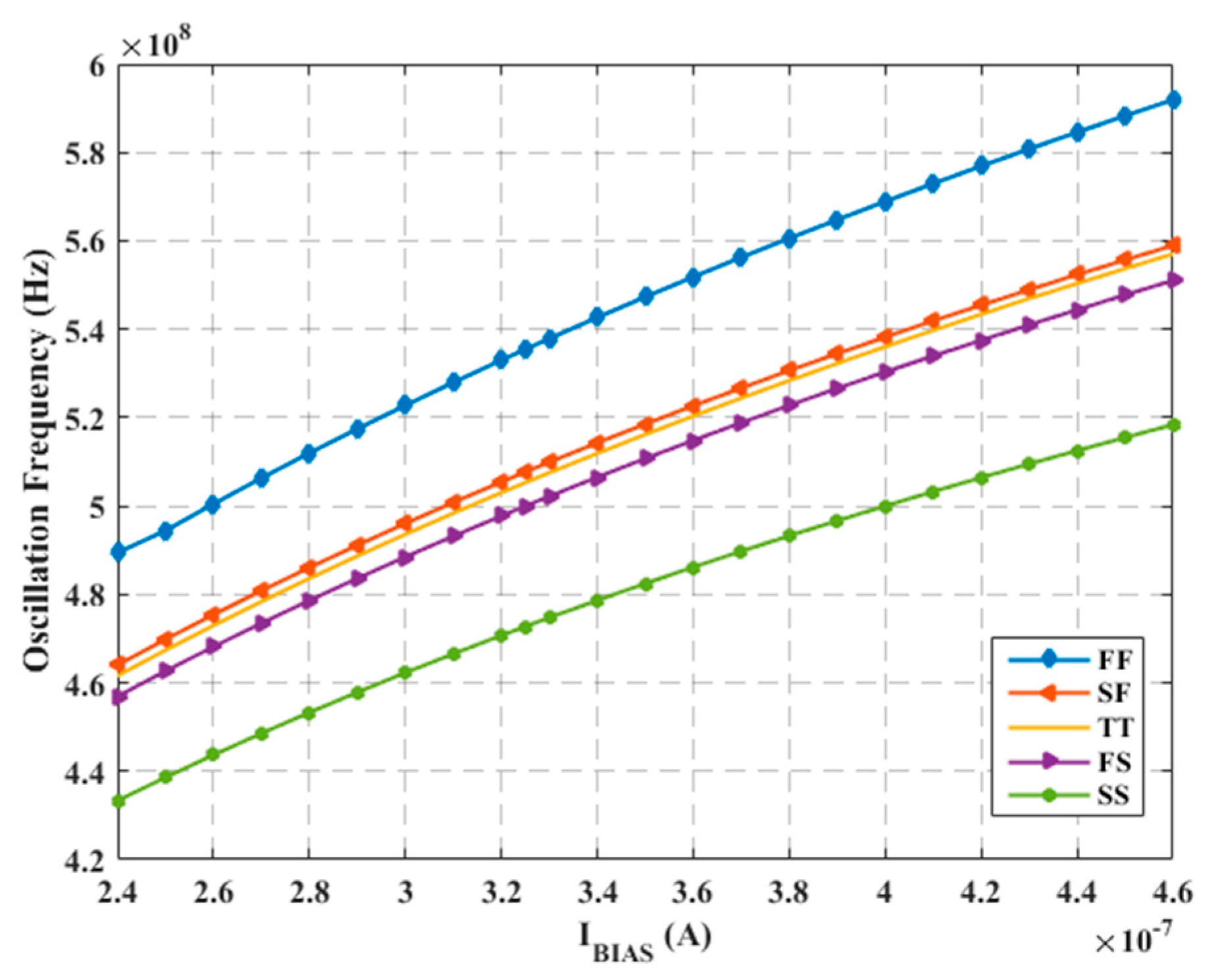
Figure 12 shows the simulated oscillation frequency of the 5-stage ring oscillator in this range of IBIAS, for the five basic corners (at 30 °C). It can be noted that the tuning frequency range is independent of the process corners. Indeed, the tuning sensitivity is constant regardless the corner and is still approximately equal to 0.43 MHz/nA. The maximum percentage variation between the nominal oscillation frequency and that affected by corners is about 20%.
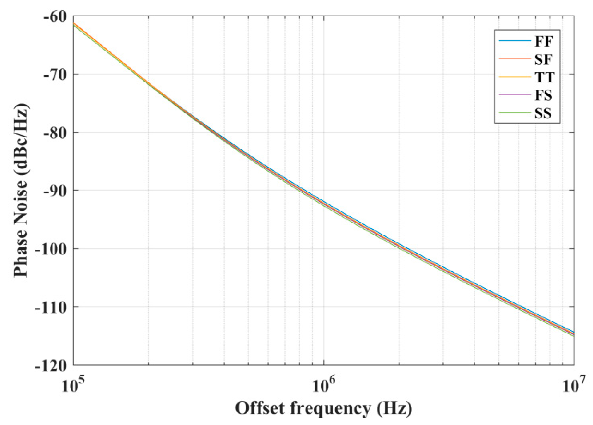
Phase noise versus offset frequency (Δf) for the basic corners is illustrated in Figure 13, which clearly shows the close overlap of the five curves, indicating that also the phase noise is process independent.
Phase noise was also simulated in the 0 °C to 60 °C temperature range and across the five corners. The minimum value of the simulated phase noise is −91.86 dBc/Hz when T = 0 °C in the FF corner, while the maximum value of the simulated phase noise is −93.72 dBc/Hz when T = 0 °C in the SS corner (both values are evaluated at the nominal bias current IBIAS equal to 350 nA).
Table 2, Table 3 and Table 4 summarize the corner analysis results of the main parameters of the simulated 5-stage current-controlled ring oscillator (nominal IBIAS equal to 350 nA and at 30 °C) for three values of the supply voltage VDD.
Due to process variations, oscillation frequency varies of about 20%. However, tuning range variations across the five corners are limited to 8% and both phase noise and average power consumption variations are 5%. Regarding power consumption, the typical (TT) value is accurately predicted by (14), where Ctot can be estimated to be 88.6 fF, including the additional load capacitance of 10 fF. This value agrees with the results shown in Figure 10b.
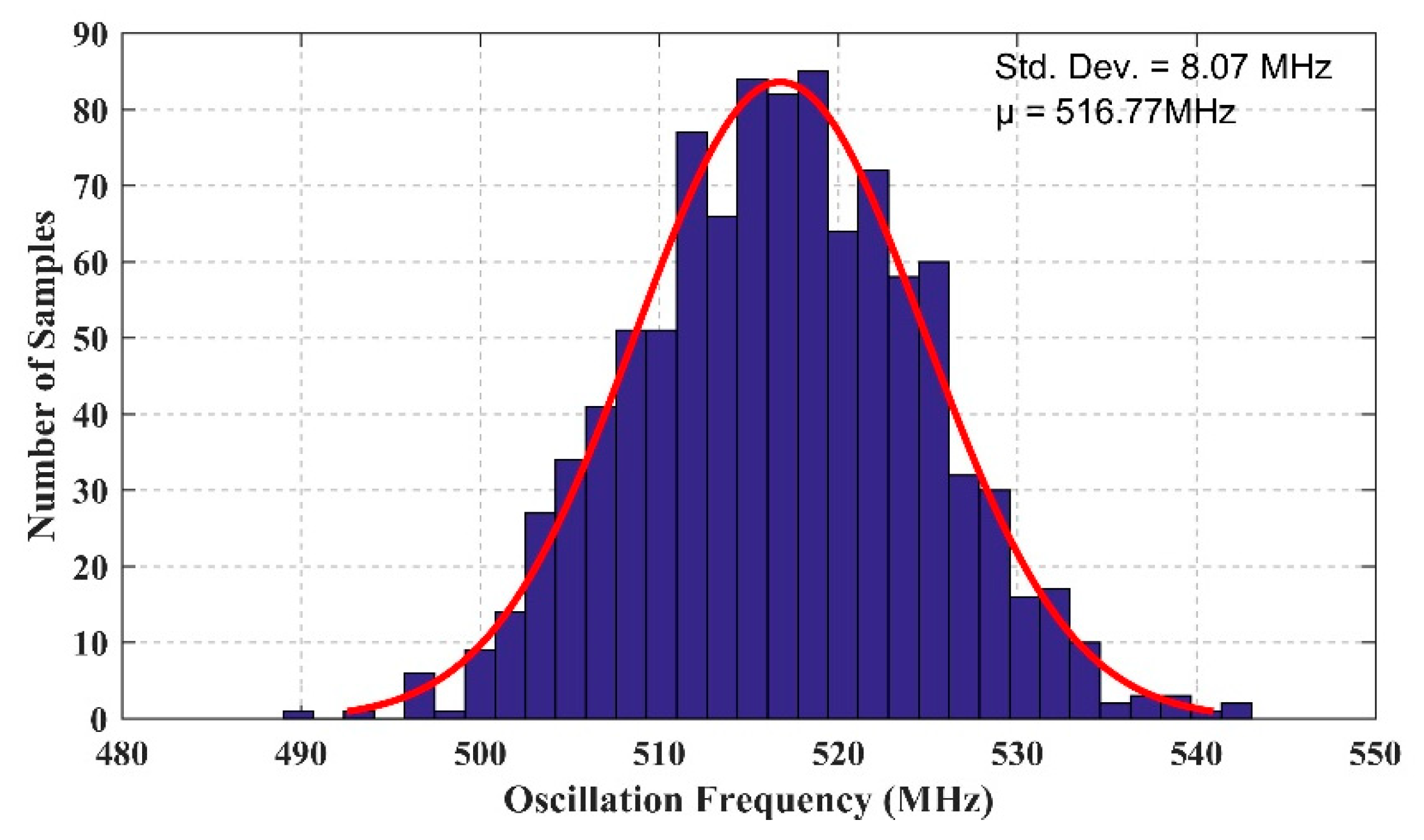
Mismatch Monte Carlo simulations of the oscillation frequency in typical conditions (VDD = 0.5 V, IBIAS = 350 nA and T = 27 °C) are reported in Figure 14, showing the limited impact of mismatches on the oscillation frequency of the proposed CRO.
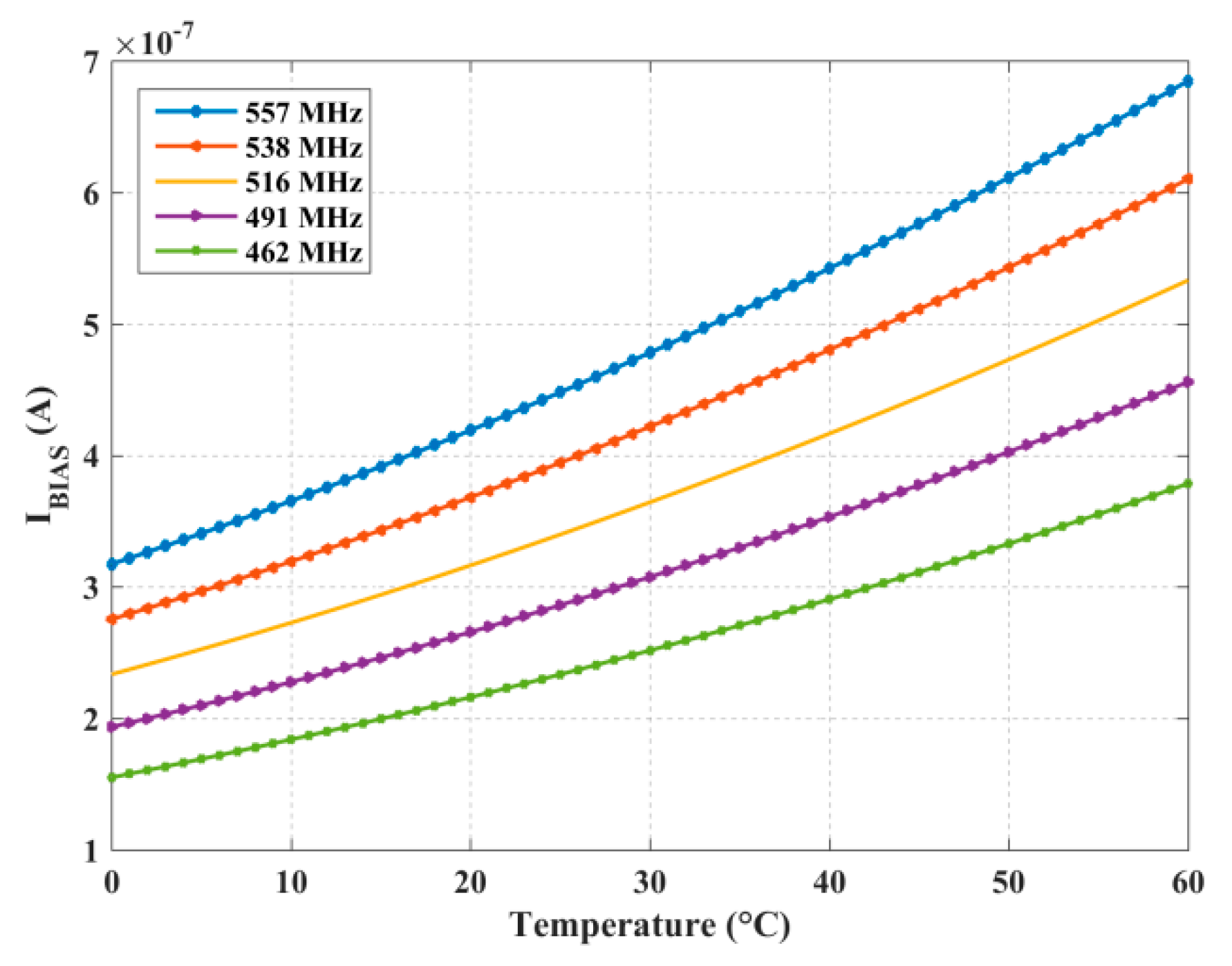
As already mentioned, the tuning capabilities of the proposed CRO can be exploited to compensate for the effects of temperature variations (in a non-exclusive alternative to process variations). To give an example, Figure 15 shows some isofrequency curves (at 557 MHz, 538 MHz, 516 MHz, 491 MHz, and 462 MHz) in IBIAS vs. temperature plot. Each point of the curves establishes the current IBIAS needed to set the target frequency between around 450 MHz and 557 MHz in the operating range from 0 °C to 60 °C.
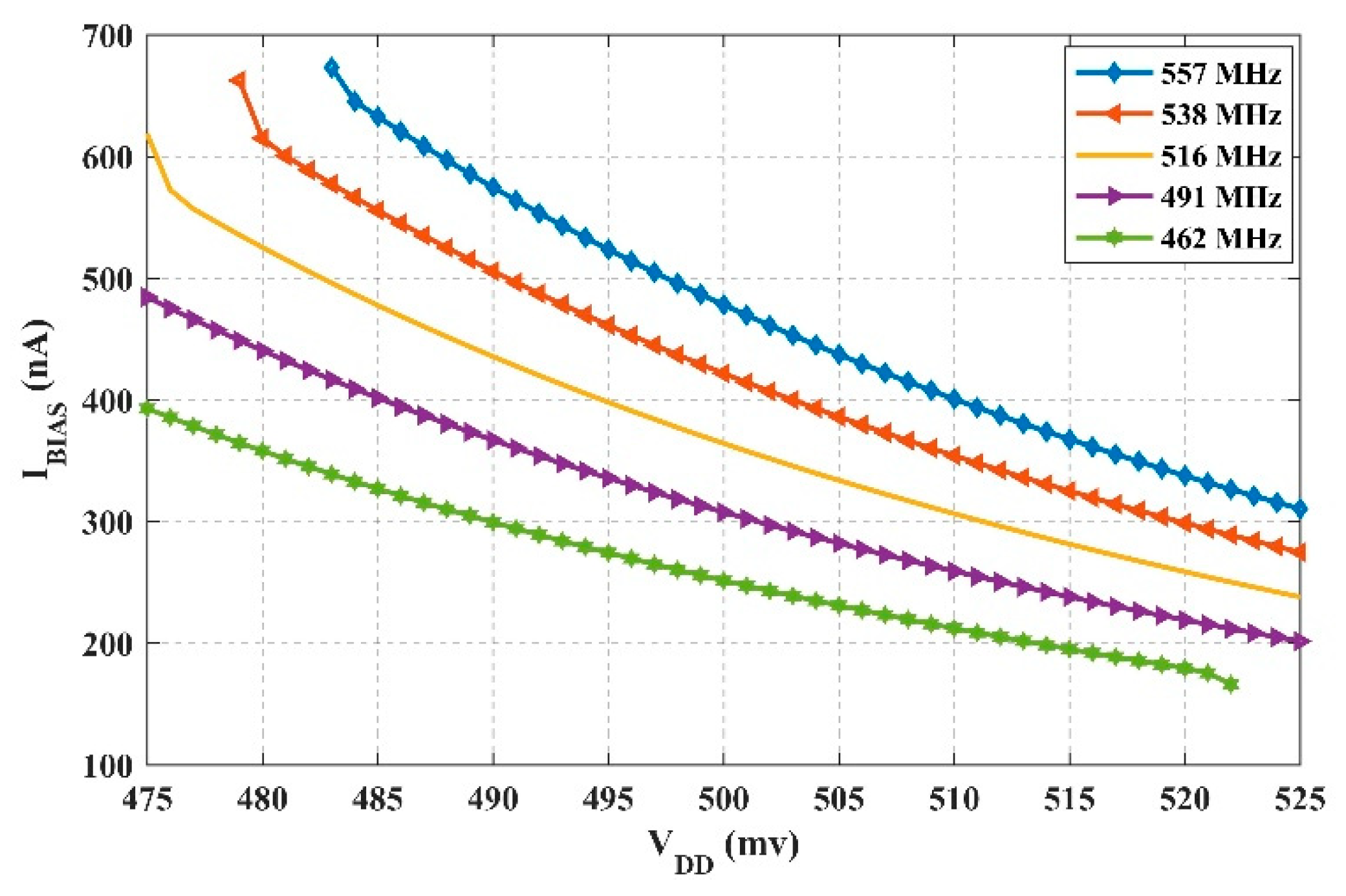
The tuning capabilities of the proposed CRO can be exploited also to compensate the effects of supply voltage (VDD) variations. To give an example, Figure 16 shows some isofrequency curves (at 557 MHz, 538 MHz, 516 MHz, 491 MHz, and 462 MHz) in the IBIAS vs. VDD plot. Each point of the curves establishes the current IBIAS needed to set the target frequency between around 450 MHz and 557 MHz in the operating range from 475 mV to 525 mV.
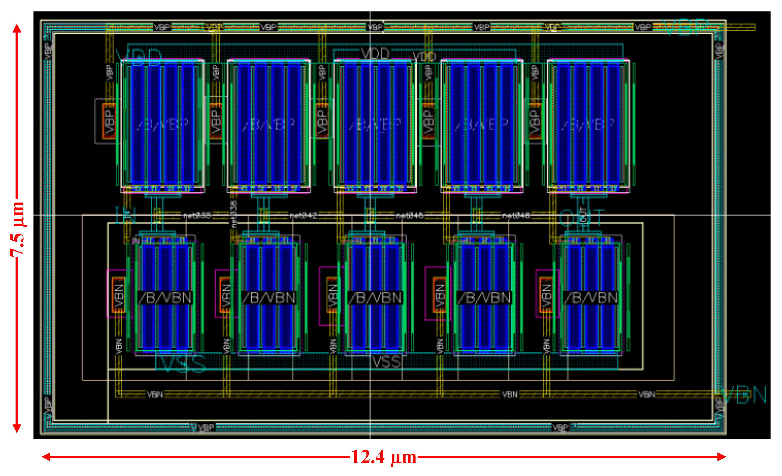
The layout of the five stage CRO is reported in Figure 17, showing an area footprint of 12.4 μm × 7.5 μm. To better assess the reliability of the above results, post layout simulations have been carried. The main effect of the layout resulted in a parasitic capacitance of 6.5 fF at the output node of the CRO. Once reduced the explicit coarse tuning capacitance of an amount equal to the parasitic capacitance, post layout simulations resulted to be in very good agreement with schematic level simulations.
Table 5 compares some recent controlled oscillator topologies presented in the literature with the proposed one, which provides the best performance in terms of phase noise and power consumption, determining the best FoM as defined by (19).
5. Conclusions
A novel approach to tune the delay of the basic inverter cell of CROs has been presented in this paper. The approach allowed to accurately set the maximum current of all the inverters in the CRO through a body bias loop and to tune the oscillation frequency by controlling the value of a reference current. Small-signal and large-signal analysis of the proposed CRO topology have been carried out to provide insight into circuit behavior and to provide useful design equations.
Current controlled ring oscillators made up of 3, 5, and 7 stages have been designed referring to a commercial 28-nm technology and with a supply voltage of 0.5 V.
Simulation results demonstrated that the proposed approach allows to optimize the tradeoff between tuning range, phase noise and power consumption, as demonstrated by the value of the FoM which outperforms all the similar designs in the literature. Extensive parametric and corner simulations have demonstrated a good robustness of the proposed CROs to PVT variations despite the adoption of a very short channel process node.
Author Contributions
Conceptualization: S.P. and G.S.; data curation: A.B. and C.V.; original draft preparation: A.B. and C.V.; writing—review and editing: all authors; supervision: S.P. and G.S. All authors have read and agreed to the published version of the manuscript.
Funding
This research received no external funding.
Institutional Review Board Statement
Not applicable.
Informed Consent Statement
Not applicable.
Data Availability Statement
The data presented in this study are available in article.
Conflicts of Interest
The authors declare no conflict of interest.
References
- Corres-Matamoros, A.; Martínez-Guerrero, E.; Rayas-Sanchez, J.E. A programmable CMOS voltage controlled ring oscillator for radio-frequency diathermy on-chip circuit. In Proceedings of the 2017 International Caribbean Conference on Devices, Circuits and Systems (ICCDCS), Cozumel, Mexico, 5–7 June 2017; pp. 65–68. [Google Scholar] [CrossRef] [Green Version]
- Ghafari, B.; Koushaeian, L.; Goodarzy, F.; Evans, R.; Skafidas, E. An ultra-low-power and low-noise voltage-controlled ring oscillator for biomedical applications. In Proceedings of the IEEE 2013 Tencon—Spring, Sydney, NSW, Australia, 17–19 April 2013; pp. 20–24. [Google Scholar] [CrossRef]
- Ranjan, R.; Raman, A.; Kashyap, N. Low Power and High Frequency Voltage Controlled Oscillator for PLL Application. In Proceedings of the 2019 6th International Conference on Signal Processing and Integrated Networks (SPIN), Noida, India, 7–8 March 2019; pp. 212–214. [Google Scholar] [CrossRef]
- Zambrano, B.; Garzón, E.; Strangio, S.; Crupi, F.; Lanuzza, M. A 0.05 mm2, 350 mV, 14 nW Fully-Integrated Temperature Sensor in 180-nm CMOS. IEEE Trans. Circuits Syst. II Express Briefs 2021, 1. [Google Scholar] [CrossRef]
- Meng, X.; Li, X.; Cheng, L.; Tsui, C.-Y.; Ki, W.-H. A Low-Power Relaxation Oscillator With Switched-Capacitor Frequency-Locked Loop for Wireless Sensor Node Applications. IEEE Solid-State Circuits Lett. 2019, 2, 281–284. [Google Scholar] [CrossRef]
- Ballo, A.; Bruno, G.; Grasso, A.D.; Vaiana, M.G.G. A Compact Temperature Sensor With a Resolution FoM of 1.82 pJ·K2. IEEE Trans. Instrum. Meas. 2020, 69, 8571–8579. [Google Scholar] [CrossRef]
- Alioto, M. (Ed.) Enabling the Internet of Things: From Integrated Circuits to Integrated Systems; Springer International Publishing: Berlin/Heidelberg, Germany, 2017. [Google Scholar] [CrossRef]
- Ballo, A.; Bottaro, M.; Grasso, A.D. A Review of Power Management Integrated Circuits for Ultrasound-Based Energy Harvesting in Implantable Medical Devices. Appl. Sci. 2021, 11, 2487. [Google Scholar] [CrossRef]
- Stornelli, V.; Barile, G.; Pantoli, L.; Scarsella, M.; Ferri, G.; Centurelli, F.; Tommasino, P.; Trifiletti, A. A New VCII Application: Sinusoidal Oscillators. J. Low Power Electron. Appl. 2021, 11, 30. [Google Scholar] [CrossRef]
- Razavi, B. A study of phase noise in CMOS oscillators. IEEE J. Solid-State Circuits 1996, 31, 331–343. [Google Scholar] [CrossRef] [Green Version]
- Zaman, K.S.; Reaz, M.I.; Haque, F.; Arsad, N.; Ali, S.H.M. Optimization of WiFi Communication System using Low Power Ring Oscillator Delay Cell. In Proceedings of the 2020 IEEE 8th Conference on Systems, Process and Control (ICSPC), Melaka, Malaysia, 11–12 December 2020; pp. 91–94. [Google Scholar] [CrossRef]
- Nayak, R.; Kianpoor, I.; Bahubalindruni, P.G. Low power ring oscillator for IoT applications. Analog Integr. Circuits Signal Process. 2017, 93, 257–263. [Google Scholar] [CrossRef]
- Lee, S.-Y.; Hsieh, J.-Y. Analysis and Implementation of a 0.9-V Voltage-Controlled Oscillator With Low Phase Noise and Low Power Dissipation. IEEE Trans. Circuits Syst. II Express Briefs 2008, 55, 624–627. [Google Scholar] [CrossRef]
- Reddy, N.; Pattanaik, M.; Rajput, S.S. 0.4V CMOS based low power voltage controlled ring oscillator for medical applications. In Proceedings of the TENCON 2008–2008 IEEE Region 10 Conference, Hyderabad, India, 19–21 November 2008; pp. 1–5. [Google Scholar] [CrossRef]
- Chuang, Y.-H.; Jang, S.-L.; Lee, J.-F.; Lee, S.-H. A low voltage 900 MHz voltage controlled ring oscillator with wide tuning range. In Proceedings of the 2004 IEEE Asia-Pacific Conference on Circuits and Systems, 2004, Tainan, Taiwan, 6–9 December 2004; Volume 1, pp. 301–304. [Google Scholar] [CrossRef]
- Srivastava, A.; Zhang, C. An Adaptive Body-Bias Generator for Low Voltage CMOS VLSI Circuits. Int. J. Distrib. Sens. Netw. 2008, 4, 213–222. [Google Scholar] [CrossRef]
- Deen, M.J.; Kazemeini, M.H.; Naseh, S. Performance characteristics of an ultra-low power VCO. In Proceedings of the 2003 International Symposium on Circuits and Systems, 2003. ISCAS ’03, Bangkok, Thailand, 25–28 May 2003; Volume 1, p. I. [Google Scholar] [CrossRef]
- Ballo, A.; Grasso, A.D.; Pennisi, S.; Venezia, C. High-Frequency Low-Current Second-Order Bandpass Active Filter Topology and Its Design in 28-nm FD-SOI CMOS. J. Low Power Electron. Appl. 2020, 10, 27. [Google Scholar] [CrossRef]
- Monsurró, P.; Pennisi, S.; Scotti, G.; Trifiletti, A. Exploiting the Body of MOS Devices for High Performance Analog Design. IEEE Circuits Syst. Mag. 2011, 11, 8–23. [Google Scholar] [CrossRef]
- Palumbo, G.; Scotti, G. A Novel Standard-Cell-Based Implementation of the Digital OTA Suitable for Automatic Place and Route. J. Low Power Electron. Appl. 2021, 11, 42. [Google Scholar] [CrossRef]
- Ballo, A.; Pennisi, S.; Scotti, G. 0.5 V CMOS Inverter-Based Transconductance Amplifier with Quiescent Current Control. J. Low Power Electron. Appl. 2021, 11, 37. [Google Scholar] [CrossRef]
- Pérez-Nicoli, P.; Veirano, F.; Rossi-Aicardi, C.; Aguirre, P. Design method for an ultra low power, low offset, symmetric OTA. In Proceedings of the 2013 7th Argentine School of Micro-Nanoelectronics, Technology and Applications, Buenos Aires, Argentina, 15–16 August 2013; pp. 38–43. [Google Scholar]
- Silveira, F.; Flandre, D.; Jespers, P.G.A. A g/sub m//I/sub D/ based methodology for the design of CMOS analog circuits and its application to the synthesis of a silicon-on-insulator micropower OTA. IEEE J. Solid-State Circuits 1996, 31, 1314–1319. [Google Scholar] [CrossRef]
- Alioto, M. Understanding DC Behavior of Subthreshold CMOS Logic Through Closed-Form Analysis. IEEE Trans. Circuits Syst. Regul. Pap. 2010, 57, 1597–1607. [Google Scholar] [CrossRef]
- Rabaey, J.M. Digital Integrated Circuits: A Design Perspective; Prentice-Hall, Inc.: Hoboken, NJ, USA, 1996. [Google Scholar]
- Rajahari, G.; Varshney, Y.A.; Bose, S.C. A Novel Design Methodology for High Tuning Linearity and Wide Tuning Range Ring Voltage Controlled Oscillator. In VLSI Design and Test; Springer: Berlin/Heidelberg, Germany, 2013; pp. 10–18. [Google Scholar] [CrossRef]
- Lee, T.H.; Hajimiri, A. Oscillator phase noise: A tutorial. IEEE J. Solid-State Circuits 2000, 35, 326–336. [Google Scholar] [CrossRef] [Green Version]
- Tianwang, L.; Jiang, J.; Bo, Y.; Xingcheng, H. Ultra low voltage, wide tuning range voltage controlled ring oscillator. In Proceedings of the 2011 9th IEEE International Conference on ASIC, Xiamen, China, 25–28 October 2011; pp. 824–827. [Google Scholar] [CrossRef]
- Saheb, Z.; El-Masry, E.; Bousquet, J.-F. Ultra-low voltage and low power ring oscillator for wireless sensor network using CMOS varactor. In Proceedings of the 2016 IEEE Canadian Conference on Electrical and Computer Engineering (CCECE), Vancouver, BC, Canada, 15–18 May 2016; pp. 1–5. [Google Scholar] [CrossRef]
- Abdollahvand, S.; Oliveira, L.B.; Gomes, L.; Goes, J. A low-voltage voltage-controlled ring-oscillator employing dynamic-threshold-MOS and body-biasing techniques. In Proceedings of the 2015 IEEE International Symposium on Circuits and Systems (ISCAS), Lisbon, Portugal, 24–27 May 2015; pp. 1294–1297. [Google Scholar] [CrossRef]
Figure 1.
Simplified schematic of the proposed current-controlled ring oscillator.

Figure 2.
Simplified schematic of the biasing section generating VBN and VBP for the RO in Figure 1.
Figure 2.
Simplified schematic of the biasing section generating VBN and VBP for the RO in Figure 1.

Figure 3.
Simplified schematic of simple mirror OTA [21] used in this work.
Figure 3.
Simplified schematic of simple mirror OTA [21] used in this work.

Figure 4.
Conventional CMOS inverter (a) and its equivalent small-signal circuit (b).

Figure 5.
Conventional CMOS inverter (a) and its static transfer behavior (b).

Figure 6.
Body voltages (a) and currents (b) in the interested current biasing range at T = 30 °C.

Figure 7.
Static currents flowing in the reference inverter vs. input voltage for different IBIAS (a), and static currents maxima vs. IBIAS (T = 30 °C) (b).
Figure 7.
Static currents flowing in the reference inverter vs. input voltage for different IBIAS (a), and static currents maxima vs. IBIAS (T = 30 °C) (b).

Figure 8.
Output signal of 5-stage CRO for three different values of biasing current at T = 30 °C.

Figure 9.
Oscillation frequency of the 5-stage CRO as a function of the biasing current at T = 30 °C.
Figure 9.
Oscillation frequency of the 5-stage CRO as a function of the biasing current at T = 30 °C.

Figure 10.
Oscillation frequencies for different coarse tuning capacitance values in the interested current biasing range (a) and for a fixed IBIAS = 320 nA (b) at T = 30 °C.
Figure 10.
Oscillation frequencies for different coarse tuning capacitance values in the interested current biasing range (a) and for a fixed IBIAS = 320 nA (b) at T = 30 °C.

Figure 11.
Bulk−source voltage of NMOS (a) and PMOS (b) transistors vs. biasing current over the 5 basic process corners.
Figure 11.
Bulk−source voltage of NMOS (a) and PMOS (b) transistors vs. biasing current over the 5 basic process corners.

Figure 12.
Oscillation frequency vs. biasing current over the 5 basic process corners.

Figure 13.
Phase noise vs. offset frequency over the 5 basic process corners.

Figure 14.
Mismatch Monte Carlo simulations of the oscillation frequency in typical conditions (VDD = 0.5 V, IBIAS = 350 nA and T = 27 °C).
Figure 14.
Mismatch Monte Carlo simulations of the oscillation frequency in typical conditions (VDD = 0.5 V, IBIAS = 350 nA and T = 27 °C).

Figure 15.
Isofrequency curves in the IBIAS vs. temperature plot (TT).

Figure 16.
Isofrequency curves in the IBIAS vs. VDD, (TT).

Figure 17.
Layout of the five stage CRO.


Table 1.
Design parameters used in simulations.
| Parameter | Value |
|---|---|
| VDD | 0.5 V |
| IBIAS | 320 a nA |
| (W/L)PA, (W/L)PR, (W/L)Pi | 8.28/0.18 μm/μm |
| (W/L)NR, (W/L)Ni | 5.4/0.18 μm/μm |
| A1, A2 | 30 dB |
| GBWA1, GBWA2 | 10 kHz |
| Ci | 10 fF |
a: This value will be changed to 350 nA after corner analysis.
Table 2.
Corner analysis of the 5-stage current-controlled ring oscillator performed at 30 °C and at VDD = 475 mV.
Table 2.
Corner analysis of the 5-stage current-controlled ring oscillator performed at 30 °C and at VDD = 475 mV.
| Corner | TT | FF | FS | SF | SS |
|---|---|---|---|---|---|
| Oscillation frequency (MHz) | 451.2 | 481.6 | 446.2 | 446.7 | 397.3 |
| Tuning range (MHz) | 87.09 | 96.38 | 50.69 | 59.24 | 24.12 |
| Phase noise @1 MHz (dBc/Hz) | −92.77 | −92.39 | −92.90 | −92.90 | −93.75 |
| Average power consumption (μW) | 23.40 | 24.41 | 23.31 | 23.14 | 20.94 |
Table 3.
Corner analysis of the 5-stage current-controlled ring oscillator performed at 30 °C and at VDD = 500 mV.
Table 3.
Corner analysis of the 5-stage current-controlled ring oscillator performed at 30 °C and at VDD = 500 mV.
| Corner | TT | FF | FS | SF | SS |
|---|---|---|---|---|---|
| Oscillation frequency (MHz) | 516.2 | 547.3 | 410.7 | 418.5 | 482.5 |
| Tuning range (MHz) | 95.44 | 102.50 | 94.11 | 94.94 | 85.08 |
| Phase noise @1 MHz (dBc/Hz) | −92.47 | −92.13 | −92.58 | −92.40 | −92.87 |
| Average power consumption (μW) | 28.6 | 29.8 | 28.4 | 28.8 | 27.5 |
Table 4.
Corner analysis of the 5-stage current-controlled ring oscillator performed at 30 °C and at VDD = 525 mV.
Table 4.
Corner analysis of the 5-stage current-controlled ring oscillator performed at 30 °C and at VDD = 525 mV.
| Corner | TT | FF | FS | SF | SS |
|---|---|---|---|---|---|
| Oscillation frequency (MHz) | 583.3 | 619.7 | 577.6 | 586.5 | 549.6 |
| Tuning range (MHz) | 102.47 | 59.27 | 81.37 | 100.50 | 93.52 |
| Phase noise @1 MHz (dBc/Hz) | −92.14 | −91.98 | −92.25 | −92.06 | −92.48 |
| Average power consumption (μW) | 36.16 | 37.93 | 35.85 | 36.29 | 34.61 |
Table 5.
Comparison with the state-of-the-art.
| Reference | [28] | [29] | [30] | This Work b |
|---|---|---|---|---|
| Tech. (nm) | 180 | 65 | 65 | 28 |
| VDD (mV) | 500 | 600 | 700 | 500 |
| N stages | 3 | 3 | 4 | 5 |
| Type of control | Voltage | Voltage | Voltage | Current |
| Osc. frequency (MHz) | 82–370 | 250–800 | 880–1360 | 360–640 |
| Phase Noise (dBc/Hz)@1 MHz | −82 | −86.38 | −90 | −92.47 |
| Power consumption (μW) | 60 | 146.2 | 360 | 28.6 |
| FoM a (dBc/Hz) | −145.6 | −153.2 | −153.6 | −164 |
a: see (16); b: simulations.
Publisher’s Note: MDPI stays neutral with regard to jurisdictional claims in published maps and institutional affiliations. |
© 2022 by the authors. Licensee MDPI, Basel, Switzerland. This article is an open access article distributed under the terms and conditions of the Creative Commons Attribution (CC BY) license (https://creativecommons.org/licenses/by/4.0/).
Share and Cite
MDPI and ACS Style
Ballo, A.; Pennisi, S.; Scotti, G.; Venezia, C. A 0.5 V Sub-Threshold CMOS Current-Controlled Ring Oscillator for IoT and Implantable Devices. J. Low Power Electron. Appl. 2022, 12, 16. https://doi.org/10.3390/jlpea12010016
AMA Style
Ballo A, Pennisi S, Scotti G, Venezia C. A 0.5 V Sub-Threshold CMOS Current-Controlled Ring Oscillator for IoT and Implantable Devices. Journal of Low Power Electronics and Applications. 2022; 12(1):16. https://doi.org/10.3390/jlpea12010016
Chicago/Turabian StyleBallo, Andrea, Salvatore Pennisi, Giuseppe Scotti, and Chiara Venezia. 2022. "A 0.5 V Sub-Threshold CMOS Current-Controlled Ring Oscillator for IoT and Implantable Devices" Journal of Low Power Electronics and Applications 12, no. 1: 16. https://doi.org/10.3390/jlpea12010016
Note that from the first issue of 2016, this journal uses article numbers instead of page numbers. See further details here.