
Chemical Stability of Metal Halide Perovskite Detectors

1
School of Electrical Engineering, University of South China, Hengyang 421001, China
2
Shenzhen Key Laboratory of Ultraintense Laser and Advanced Material Technology, Center for Intense Laser Application Technology and College of Engineering Physics, Shenzhen Technology University, Shenzhen 518118, China
*
Authors to whom correspondence should be addressed.
†
These authors contributed equally to this work.
Inorganics 2024, 12(2), 52; https://doi.org/10.3390/inorganics12020052
Submission received: 31 December 2023
/
Revised: 25 January 2024
/
Accepted: 30 January 2024
/
Published: 3 February 2024
(This article belongs to the Section Organometallic Chemistry)
Abstract
:Metal halide perovskite (MHP) detectors are highly esteemed for their outstanding photoelectric properties and versatility in applications. However, they are unfortunately prone to degradation, which constitutes a significant barrier to their sustained performance. This review meticulously delves into the causes leading to their instability, predominantly attributable to factors such as humidity, temperature, and electric fields and, notably, to various radiation factors such as X-rays, γ-rays, electron beams, and proton beams. Furthermore, it outlines recent advancements in strategies aimed at mitigating these detrimental effects, emphasizing breakthroughs in composition engineering, heterostructure construction, and encapsulation methodologies. At last, this review underscores the needs for future improvements in theoretical studies, material design, and standard testing protocols. In the pursuit of optimizing the chemical stability of MHP detectors, collaborative efforts are in an imperative need. In this way, broad industrial applications of MHP detectors could be achieved.
1. Introduction
Metal halide perovskites (MHPs) have emerged as prominent candidates for various technological applications, including solar cells, light-emitting diodes, detectors, and lasers [1,2,3]. In recent years, they have been recognized as promising detectors due to their unique multi-field coupling response and photoelectric conversion, electro-optic conversion, and all-optical conversion characteristics. Notably, in contrast to traditional semiconductor materials [4,5], MHP detectors offer several advantages in the detection field [6,7]. Their exceptional carrier mobility (2000 cm2 V−1 s−1) ensures efficient charge transfer within materials [8], leading to a rapid response. Additionally, the long diffusion length (175 μm) of the charge carriers facilitates an effective charge collection [9], thereby enhancing the overall detector performance. Furthermore, the ability of MHP materials to incorporate atoms with a high atomic number (e.g., Pb, Cs, Sn, I, and Br) allows for the absorption of high-energy radiation, making them well-suited for radiation detection applications. Moreover, the tunable bandgap (1.17–3.46 eV) of MHPs enables customization to meet specific detection requirements [2,10,11], extending their utility across various wavelength and energy ranges. Additionally, the low trap density (107–109 cm−3) of single crystalline perovskite-based detectors improves the signal-to-noise ratio [12], crucial for achieving accurate and sensitive detection. This collective suite of characteristics makes MHP detectors promising candidates for various detection applications, such as in photodetectors and X-ray detectors [13,14].
At present, MHPs have been used to construct direct and indirect detectors. In the case of MHP-based direct detectors, a common configuration involves a sandwiched structure insetting an MHP layer between two electrodes. The MHP layer acts as the active material that absorbs incident photons or radiation. When photons or radiation interact with the MHP layer, it generates electron–hole pairs, leading to the formation of excited charge carriers. The resulting charge carriers are then collected by the electrodes and generate a measurable electrical signal. Direct detectors typically offer higher quantum efficiency, higher spatial resolution, and faster response time compared to indirect detectors [14,15]. As for indirect detectors, an MHP scintillator material is employed. MHP scintillators absorb the incident radiation and generate visible light as a result of the radiative recombination of excited electrons and holes. This visible light signal is then detected by the photodetector, typically a photomultiplier tube or a solid-state detector. The photodetector converts the optical signals into electrical signals for further processing. MHP-based indirect detectors generally have lower quantum efficiency and spatial resolution compared to direct detectors but can offer superior sensitivity to low-energy radiation and a better signal-to-noise ratio in certain imaging applications [16,17].
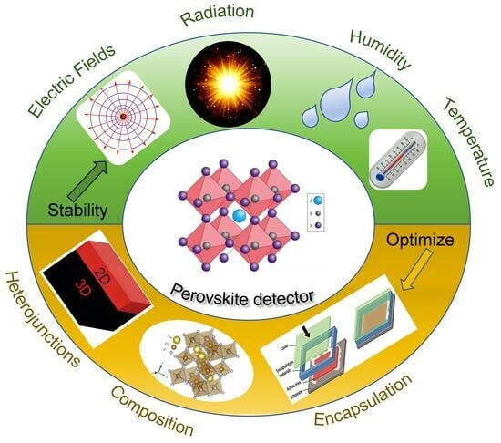
However, despite their numerous advantages, MHP detectors face challenges related to their chemical stability. The susceptibility of these materials to degradation under ambient or detection conditions poses a significant obstacle to achieve their long-term performance and practical implementation. Factors such as humidity, temperature, electric fields, and radiation (Figure 1) can lead to the formation of undesired phases or the liberation of harmful species, resulting in a decline in device performance and lifetime [18,19]. In view of this, stability is pivotal not only for prolonging the operational life of MHP detectors but also for ensuring their consistent and reliable performance across diverse detection conditions. As detectors find applications in critical fields such as medical sensing and industrial monitoring, the reliability of the derived results becomes paramount. A nuanced exploration of stability challenges and their mitigation strategies will contribute to the ongoing efforts to make MHP detectors robust and deployable in real-world scenarios.
Several review articles have been published on the degradation mechanisms of MHPs in solar cells [20,21,22,23]. These comprehensive reviews offer valuable insights into the degradation processes and mechanisms of perovskite materials in solar cells, with a particular emphasis on factors such as humidity, light, and heat. At present, limited attention has been given to the influence of radiation factors on MHPs, making it a relatively less explored area in existing review articles. Therefore, this review article aims to fill this gap by discussing the latest research on the degradation mechanisms of MHPs, specifically focusing on the impact of radiation factors. By including radiation factors, this review article provides a more comprehensive understanding of the degradation mechanisms of perovskite materials in various environmental conditions.
Once the significance of addressing stability issues to unlock the full potential of MHP detectors is recognized, a comprehensive review focused on chemical stability becomes imperative. This review aims to delve into the existing literature, synthesizing the available knowledge to provide a thorough understanding of the stability-affecting factors encountered by MHP detectors (Figure 1). Beyond the identification of these factors, this review will numerate the advances made in stabilizing MHP materials through diverse approaches, including composition engineering, innovative heterostructures, and effective encapsulation strategies.
2. Degradation Factors Impacting MHP Detectors
The stability of MHP material is paramount as it directly impacts the reliability and accuracy of the detector. However, the stability of MHPs is susceptible to various environmental factors such as temperature, radiation, oxygen, and other factors. This review aims to analyze and elucidate the influence of these factors on the stability of MHP materials. By exploring the mechanisms behind their impact, we can gain a comprehensive understanding of the joint effect that different factors have on MHP materials. Additionally, comprehensive explanations regarding the unavoidable radiation factors in the detector application scenarios will be provided, offering a detailed account of their effects.
2.1. Radiation
2.1.1. Ultraviolet and Visible Light
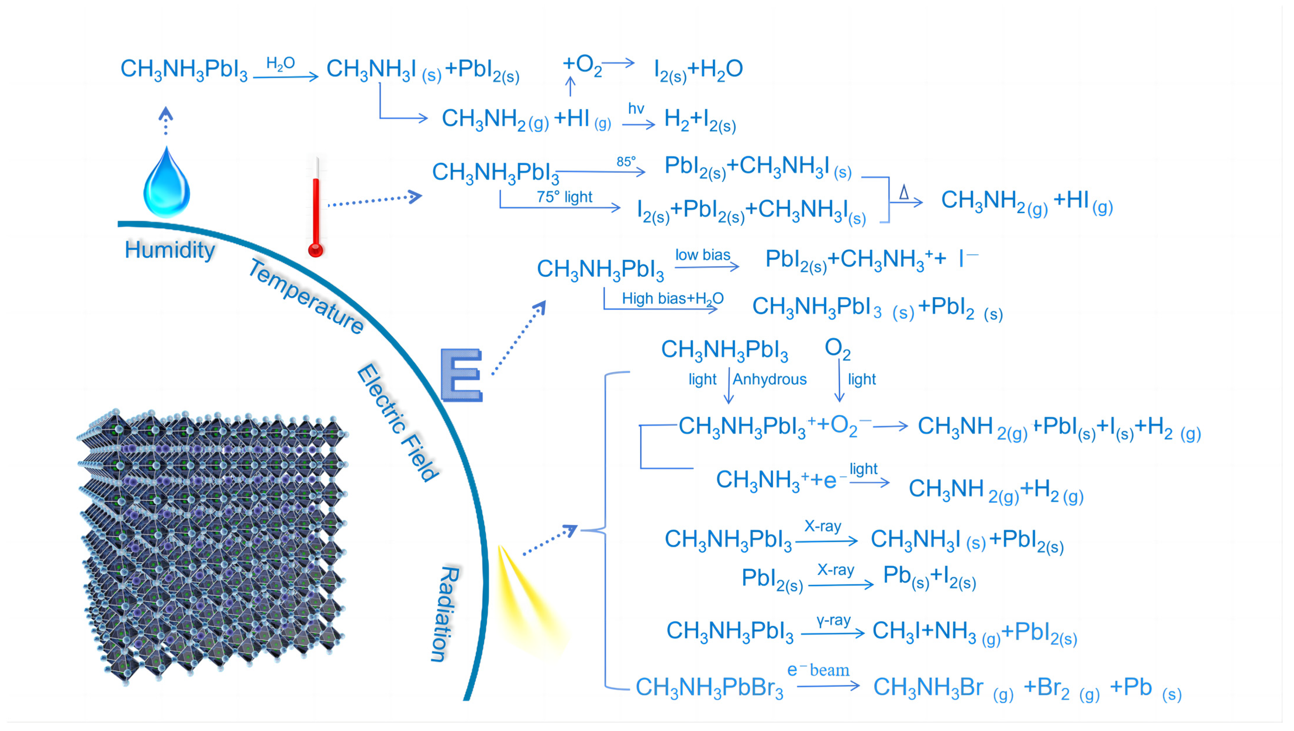
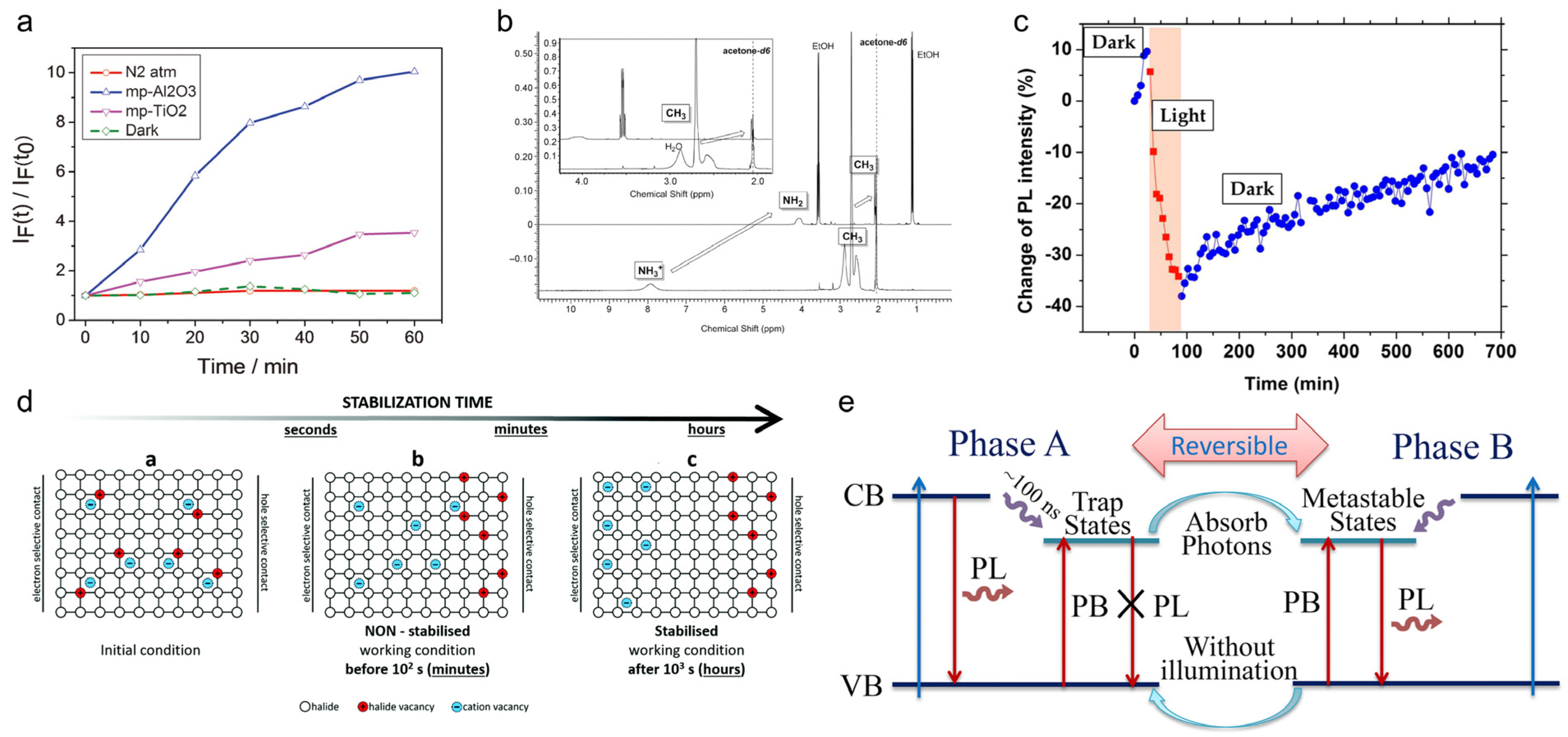
The degradation of MAPbI3 by light radiation can occur in two conditions: aerobic and anaerobic. Aristidou further deeply analyzed the mechanism of the oxygen–light degradation process [23]. The decomposition of MAPbI3 by O2 primarily occurs due to the irradiation of ultraviolet (UV) and visible (VIS) light, which excites the photoelectrons in MAPbI3. Subsequently, O2 captures these photoelectrons, forming peroxy ions (O2−). Thus, O2− further deprotonates CH3NH3+. This mechanism was verified by Aristidou, who conducted experiments in four distinct conditions: in pure N2, in the dark, with an Al2O3− covering layer, and with a TiO2− covering layer. Fluorescence molecular probe analysis found that MAPbI3 decomposition was practically absent in both the pure N2 environment and the dark environment. Furthermore, the decomposition rate was higher when Al2O3 was used as a covering layer compared to TiO2 (Figure 2a). To further confirm the mechanism by which O2− acts upon CH3NH3+, a solution of MAI in anhydrous ethanol was subjected to hydrogen NMR analysis after the addition of potassium peroxide (KO2). The analysis revealed the oxidation of CH3NH3+ to methylamine (MeNH2) by O2−, as depicted in Figure 2b. The specific influence mechanism of light is summarized as follows:
In addition to the previously mentioned role of light radiation in aiding oxygen-induced perovskite decomposition, it was found that light radiation in an oxygen-free environment can generate peroxy ions (O2−). Subsequently, O2− will assist CH3NH3+ to capture the charge of the N–H antibonding state, leading to decomposition. In the absence of oxygen, ultraviolet radiation alone can induce the dissociation of organic cations, resulting in the generation of highly mobile CH3NH2 (MA). The process involves the abstraction of an H atom from NH3, which can occur when an electron occupies one of the antibonding orbitals; in an isolated NH3 molecule, a considerable excitation energy would be required for an electron to transition from a bonding to an antibonding orbital, surpassing typical photon energy levels. However, in CH3NH3PbI3 perovskites, the organic ions occupy regular lattice sites. Consequently, in the solid state, the molecular orbitals form energy bands that contribute to the overall band structure. Nickel et al. demonstrated that a photon energy (UV light, >3 eV) is enough to excite electrons from the valence band edge into the antibonding orbitals of NH3 [19], resulting in the dissociation of an N–H bond. Consequently, the H atom is released from the NH3 group of the organic ions, leading to the formation of highly mobile MA and hydrogen ions. It is worth noting that compared to the reaction in aerobic conditions, this reaction usually requires higher energy photons (UV light) [24]. The specific mechanism is as follows:
Taking MAPbI3 as an example, the migration of MA+ leads to the collapse of the MAPbI3 lattice to produce PbI2, and the subsequent reduction of Pb2+ will continue to produce Pb and I2. Interestingly, subsequent research revealed that radiation exposure can induce two distinct types of perovskite degradation: reversible and irreversible. Gottesman et al. investigated this phenomenon by continuously monitoring the PL spectra of MAPbI3 films under light or no light in a dry N2 environment [25]. As shown in Figure 2c, the intensity of the MAPbI3 PL spectra sharply declined within 100 min of light exposure. But the PL intensity gradually recovered after the exposure of MAPbI3 to darkness. Nie et al. explained this observation by proposing that radiation exposure generates numerous metastable defects within the perovskite film, and their accumulation contributes to the decline in the film performance. However, after returning to darkness, such metastable defects would disappear spontaneously, leading to the observed recovery [26]. Domanski et al. put forth a systematic and distinct explanation for this phenomenon [27]. They attributed the reversible part of this phenomenon to ion migration. They suggested that light caused the migration of both halide ions and cation vacancies, which led to the deterioration of the device performance. Upon returning to darkness, the migrated ions returned to their original position as a result of the action of the internal electric field (Figure 2d) [27]. While both explanations for the reversible part of the described phenomenon are plausible, there is currently a lack of relevant reports concerning the irreversible part.
Figure 2.
(a) IF(t) is the maximum fluorescence intensity at time t, and IF(t0) is the background fluorescence intensity of the probe at time t = 0. The ratio IF(t)/IF(t0) is the yield of superoxide products. (b) NMR spectra of an MAPbI3 sample (bottom) and spectra after adding potassium superoxide (Both the signal for the NH3+ and the methyl group protons shift up-field upon addition of potassium superoxide, which is consistent with the deprotonation of the ammonium group to form methylamine (MeNH2)) [23]. For details, see ref. [23]. Reprinted with permission from ref. [23]. Copyright 2015 Angew. Chem. Int. Ed. (c) The PL intensity of MAPbI3 dropped sharply under light conditions and slowly recovered after returning to darkness [25]. For details, see ref. [25]. Reprinted with permission from ref. [25]. Copyright 2015 J. Phys. Chem. Lett. (d) Schematics of the evolution of ion distribution under light irradiation [27]. For details, see ref. [27]. Reprinted with permission from ref. [27]. Copyright 2017 Energ. Environ. Sci. (e) The new band inserted provides a model for the migration of X elements [28]. For details, see ref. [28]. Reprinted with permission from ref. [28]. Copyright 2016 Org. Electron.

The light radiation-induced phase separation described above is not applicable to all perovskite materials but is specific to mixed halide perovskites. Using CH3NH3PbBrxI(3−x) as an example, researchers can regulate the band gap of the material by adjusting the halogen ratio [28]. When x > 0.6, the energy provided by light triggers the aforementioned halide ion migration in the degradation process, resulting in phase separation and the formation of a bromine-rich phase and an iodine-rich phase. This phase separation was clearly observed in the X-ray diffraction (XRD) peaks, both before and after radiation irradiation, with the appearance of new peaks corresponding to the bromine-rich and iodine-rich phases. Upon returning to darkness, the phenomenon of phase separation gradually diminishes, and this can be attributed to the presence of the internal electric field mentioned below. Further studies into phase separation revealed a fascinating observation that contrasts with the degradation mechanism. Surprisingly, it is not the radiation with higher energy that is predominantly responsible for inducing the phase separation phenomenon. Yang et al. demonstrated that defects within MHPs capture photons with specific energy, consequently introducing new energy bands within the existing band gap. This particular process facilitates the migration of the halide element (Figure 2e) [28].
The occurrence of phase transitions induced by light radiation can be attributed to the nature of the phase transitions in MHPs. MHPs have a special octahedral structure due to a special bonding between ions. However, this structure can undergo various structural distortions in response to changes in the bonding forces, thereby leading to phase transitions. The generated phase transitions are typically affected by external forces such as electric fields and an increase in chemical bond energy due, for example, to temperature or radiation exposure. By considering the aforementioned theoretical framework, it becomes evident that the forces driving the phase transitions are closely linked to the external forces or the energy applied [29,30]. The phase transitions observed under light irradiation may occur due to the generation of photo-generated carriers, which in turn induce lattice dilation in the material. In the case of MAPbI3 [26], when subjected to above-bandgap light radiation, there is a charge transfer from the hybridized Pb 6s–I 5p orbital to the Pb 6p orbital. This electronic transition directly reduces the electron density on the I site, consequently weakening the Coulomb interaction with the amine group. Thus, the Pb-I-Pb bond becomes straightened, leading to an increased interatomic spacing that facilitates phase transitions. Additionally, intense light radiation above the bandgap triggers a fast electron–phonon coupling and Auger heating, which will rapidly deposit energy into the lattices, thereby inducing phase transitions in MHPs [27].
2.1.2. X-ray
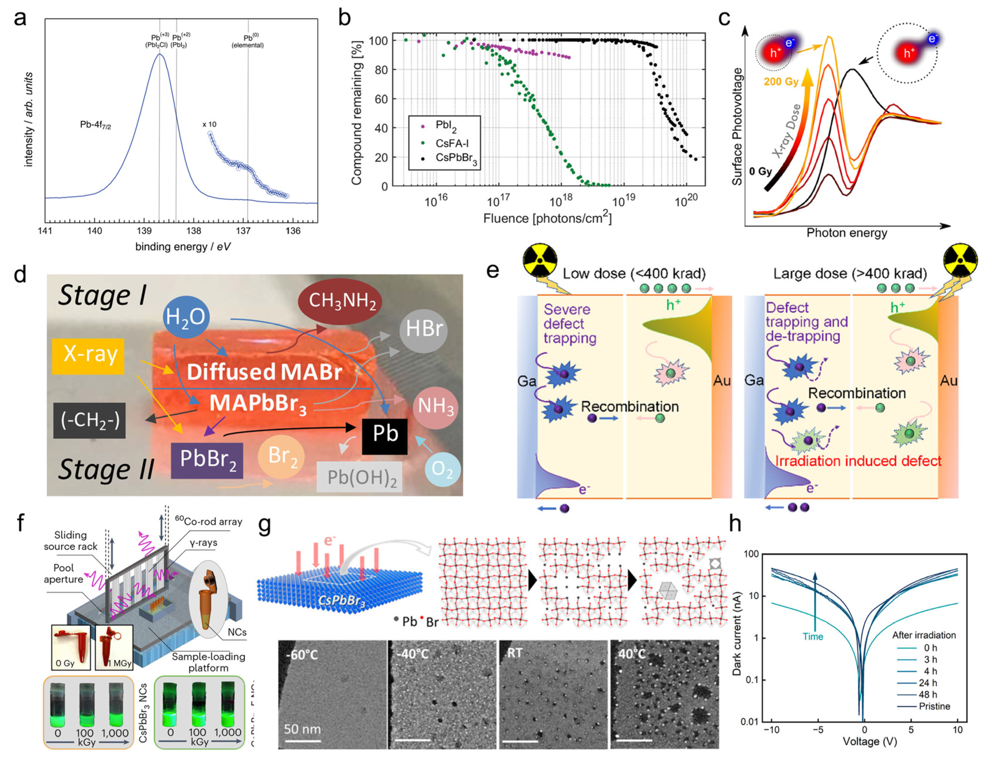
X-ray-induced damages to MHP materials were initially observed through X-ray photoelectron spectroscopy (XPS) detection. Conings et al. detected the presence of elemental lead (Pb0) in high-resolution XPS observations (Figure 3a) [31]. Shkrob et al. further explained that this elemental lead arose from the radiation-induced decomposition caused by hard X-rays during XPS detection [32]. Moreover, the detrimental effects of X-ray radiation were prominently observed at high temperatures [33]. Recently, perovskite materials have gained significant attention as potential candidates for X-ray detectors, thereby bringing the issue of X-ray stability into focus. Lin et al. employed the XPS technology to examine the degradation process of a CH3NH3PbI3 thin film induced by soft X-rays in vacuum [34]. The degradation of the perovskite film was observed to occur rapidly, with prolonged irradiation, resulting in the production of elemental lead. The degradation process is as follow:
Recently, Cappel et al. conducted an investigation on the radiolysis of MHPs using hard X-ray irradiation generated by a synchrotron accelerator [35]. The study revealed that inorganic perovskites own higher stability compared to those containing organic cations. The hybrid Cs0.17FA0.83PbI3 perovskite underwent decomposition at an irradiation dose in the range of 1016–1017 photons per cm2, whereas inorganic CsPbBr3 exhibited decomposition at a dose of 1019 photons per cm2 (Figure 3b). Moreover, the decomposition mechanisms of the two materials also differed. In the case of CsPbBr3, the decomposition reaction proceeded as follows:
However, for the Cs0.17FA0.83PbI3 material, the authors observed a lead/halide ratio of 1:2 in the radiation product, and no metallic lead was formed. Consequently, they proposed that X-ray-induced decomposition involves two pathways. One pathway is associated with the radiative decomposition of lead halide cages, resulting in the formation of halide salts, halogen gases, and metallic lead. This decomposition process seems to be influenced by defects present in the perovskite structure. On the other hand, another pathway is induced by the radiolysis of organic cations, leading to the generation of organic degradation products and the subsequent collapse of the perovskite structure. In addition to utilizing the XPS technology for detecting the effects of X-ray irradiation, Huang et al. directly investigated the performance of the Cs0.1FA0.9PbI3 material under X-ray irradiation (X-ray tube: 120 kV, 3 mA) [36]. The authors attributed the observed X-ray-induced damage to lattice defects, specifically, I− displacement, which was caused by secondary electrons generated during radiation. The comparable responses observed in both e-beam and X-ray irradiations provided a confirmation that the X-ray-induced radiation damage may originate from secondary electrons generated by X-rays.
To eliminate the potential influence of grain boundaries, it is crucial to investigate the impact of X-ray radiation on the surface of single crystals rather than on thin films. Motoki et al. investigated the impact of soft X-ray irradiation on CH3NH3PbI3 single crystals and observed the evaporation of methylamine iodide from the crystal surface [37], leaving on it polycrystalline lead iodide. The decrease in device performance caused by X-ray irradiation stabilized after 40 h of continuous exposure. However, in a recent study by Armarali et al. [38], it was found that the irradiation of MAPbBr3 single crystals (up to 200 Gy) in an air environment did not result in the formation of metallic lead. Furthermore, surface photovoltage spectroscopy unveiled that X-ray irradiation can quench free excitons within the material and introduce new bound exciton species (Figure 3c). The corresponding reaction is depicted as follows:
Gao et al. conducted research on the effect of X-ray radiation on a single crystal of MAPbBr3 in a vacuum environment, revealing that approximately 10% of the surface MAPbBr3 was degraded into metallic lead (Figure 3d) [39]. Furthermore, recent work by Cappel et al. delved deeper into the effects of X-ray radiation on single crystals comprising different components under vacuum conditions [40]. Those findings indicated that only a small amount of metallic lead was formed in MAPbI3 and CsPbBr3 single crystals. On the other hand, MAPbCl3, MAPbBr3, and FAPbBr3 single crystals exhibited the formation of a significant quantity of metallic lead, which continuously increased during the experimental process. Moreover, the X-ray radiation-induced degradation mechanisms varied among different single crystals. Specifically, the degradation of MAPbI3 and MAPbCl3 followed distinct primary degradation pathways, i.e., radiolysis, leading to the formation of PbI2 and Pb0, respectively. In contrast, MAPbBr3, FAPbBr3, and CsPbBr3 experienced multiple parallel degradation processes, including the formation of metallic lead, the generation of volatile and solid degradation products, and ion migration (shown below). Collectively, these results highlight the diverse and intricate nature of X-ray-induced degradation processes in different components of perovskite materials, underscoring the need for further comprehensive research in this area.
Based on the results in the above-mentioned literature, the X-ray-induced radiolysis of MHP structures involves two distinct pathways, from a microscopic mechanism perspective. In the first pathway, X-ray irradiation causes the radiative decomposition of lead halide cages. High-energy X-rays interact with the lead halide cages, leading to the breakage of bonds within the cages. This decomposition process is influenced by defects present in the perovskite structure, which can act as nucleation sites for the decomposition reaction. As a result of this decomposition, halide salts, halogen gases, and metallic lead can be formed. The formation of these products may occur due to the release of halides from the broken lead halide cages, leaving behind metallic lead and generating halide salts and halogen gases as by-products. On the other hand, the second pathway involves the radiolysis of organic cations present in the perovskite structure. When X-rays interact with organic cations, chemical reactions take place, resulting in the generation of organic degradation products. These organic degradation products are formed as a consequence of the fragmentation and rearrangement of the organic cations induced by X-ray radiation. As the accumulation of these degradation products continues, it ultimately leads to the collapse of the perovskite structure, causing a deterioration of the overall material integrity. Collectively, these results highlight the diverse and intricate nature of X-ray-induced degradation processes in different components of perovskite materials, underscoring the need for further comprehensive research in this area.
2.1.3. γ-ray
In 2019, Yang et al. reported a remarkable 96.8% efficiency retention in Cs0.05FA0.81MA0.14PbI2.55Br0.45 perovskite devices even after high-dose γ-ray radiation (2.3 Mrad) over a period of 1535 h [41]. However, subsequent research conducted by Boldyreva et al. demonstrated a performance decrease of 32–41% in Cs0.15MA0.10FA0.75Pb(Br0.17I0.83)3 perovskite devices subjected to γ-ray radiation (0–50 krad) [42]. The researchers observed a red shift and enhanced luminescence, which they attributed to phase separation induced by γ-ray radiation. Yang et al. also observed a similar phase separation of perovskite materials and a noticeable decrease in the absorption of perovskite under γ-ray radiation (100–500 krad) [43]. Boldyreva et al. further examined the effects of γ-ray radiation (0–1000 krad) on perovskite materials with different compositions. They observed surface decomposition in MAPbI3 and CsPbI3 under irradiation [44], according to the following the decomposition reaction:
Furthermore, they found that the radiation damage inflicted upon MAPbI3 was reversible, highlighting the significant self-healing properties of MAPbI3 when placed in darkness. It should be noted that most of the aforementioned studies were based on perovskite polycrystalline films, which may have introduced interference due to grain boundaries and a multitude of defects. To mitigate these interferences and gain a more accurate understanding of the influence of γ-ray irradiation on MHPs, the use of single crystals is preferred. Xu et al. investigated the effects of γ-ray irradiation (1656 krad) on CH₃NH₃PbBr₃ single crystals and observed a significant decrease in light transmittance [45]. Gao et al. studied the impact of γ-ray irradiation on FA0.95Cs0.05PbI2.7Br0.3 single crystals and found that their photoelectric performance remained relatively unaffected and the material was capable of self-healing when the radiation dose was below 200 krad [46]. However, when the dose exceeded 400 krad, a noticeable decrease in device performance was observed.
In comparison to organic–inorganic hybrid perovskites, inorganic CsPbBr3 materials exhibit superior tolerance to γ-ray radiation. Yan et al. conducted investigations revealing that CsPbBr3 single crystals could withstand γ-ray irradiation of up to 800 krad [47]. They further observed a dose-dependent hardness in CsPbBr3 single-crystal devices (Figure 3e), particularly at high radiation doses (>400 krad). Notably, hole-type devices suffered greater damage compared to electron-type devices. De Siena et al. even discovered that high-quality CsPbBr3 single crystals grown via the Bridgman method exhibited no changes in properties under γ-ray irradiation up to 1 MRad [48]. This outcome suggests that higher γ-ray radiation tolerance can be achieved when the crystal itself possesses fewer defects. Furthermore, they observed that high doses of irradiation (10 Mrad) generated ionization damages which could destroy the electrode or the electrode–perovskite material interface, rendering the device nonfunctional. This issue underscores the importance of critical considerations in the preparation of radiation detector devices.
Inorganic scintillator perovskite materials also display remarkable tolerance to γ-ray radiation. Zaffalon et al. validated that CsPbBr3 nanocrystals maintained their initial radioluminescence efficiency and scintillation performance even under extreme γ-ray doses (up to 10,000 krad) (Figure 3f) [49]. In a recent study, Gao et al. investigated the γ-ray radiation tolerance of a Cs3Cu2I5 single-crystal scintillator and observed that the scintillation mechanism remained unchanged at high irradiance (800 krad) [50], although the photoluminescence (PL) intensity decreased. Interestingly, they discovered that the most significant performance degradation occurred within the low γ-ray radiation dose range from 400 to 600 krad. They speculated that this might be attributed to defects induced by low-dose irradiation, which could potentially be repaired at higher doses. Currently, the stability of MHPs under γ-ray radiation remains a topic of ongoing debate, particularly in regard to the recently reported exceptional tolerance to extreme γ-ray radiation [51]. The results of γ-ray radiation tolerance and the corresponding radiation damage mechanisms are subject to substantial variations due to differences in material composition, defect density, size (nano, thin film, single crystal), and even testing conditions. Therefore, further research is required to elucidate these factors and gain a deeper understanding of the γ-radiation tolerance exhibited by perovskite materials.
2.1.4. Electron Beams
Electron beam radiation is known to significantly compromise the stability of perovskite materials, as evidenced by transmission electron microscopy (TEM) analyses. Dang et al. observed a clear degradation of CsPbBr3 nanocrystalline structures under high-energy (80/200 keV) electron radiation [52]. This radiolysis process involved the destruction of a fraction of bromine atoms and the reduction of a fraction of Pb2+ ions to Pb0, which was also observed after applying other types of irradiation, such as X-rays. Subsequently, Pb0 atoms diffused and aggregated to form Pb nanoparticles (Figure 3g). The temperature rise induced by the electron beam further accelerated the diffusion and aggregation of Pb atoms, ultimately leading to the formation of Pb nanoparticles. Chen et al. also demonstrated the rapid degradation of inorganic perovskite (CsPbI3) films caused by electron beam radiation (80/200 keV) [53], even at extremely low doses (10 e−/(Å2s) for 4 min). Similarly, Syafutra et al. irradiated CH3NH3PbBr3 single crystals with a 15 keV electron beam under ultra-high vacuum [54]. They found that the surface components of the single crystals changed from MAPbBr3 to MABr, Br2, and Pb. The reaction formula is as follows:
However, the researchers observed that the structural damage to the CH3NH3PbI3 film primarily occurred at the periphery of the irradiation area, while the structure within the irradiation area remained relatively intact. Huang et al. and Miyazawa et al. found that high-energy (1 MeV) electron irradiation only caused a slight decline in the performance of perovskite thin-film devices [55,56]. This observation might be attributed to the fact that such high-energy electrons penetrate all layers within the device without directly inducing ionization and damaging the thin perovskite film. Further comprehensive investigations are warranted to delve into the structural changes and associated mechanisms occurring in materials when subjected to electron irradiation across various energy ranges.
2.1.5. Proton Beams
MHPs have demonstrated remarkable radiation tolerance to proton irradiation, with significantly lesser adverse effects compared to those induced by electron irradiation. This disparity can be attributed to the substantial difference in mass between protons and electrons (positively charged hydrogen nuclei, over 2000 times heavier than electrons), resulting in lower material damage caused by proton collisions compared to electron collisions. High-energy protons within the MeV range are the primary form of ionizing radiation encountered in space environments. In light of this, Lang et al. conducted device performance tests under high-energy proton (68 MeV) irradiation and found that the perovskite absorber could withstand proton doses up to 1012 p cm−2 [57], exceeding the damage threshold of c-Si by three orders of magnitude. Furthermore, Lang et al. confirmed that high-energy proton (20/68 MeV) radiation minimally affected device performance. However, they found that 68 MeV proton radiation contributed to a slower decay in open circuit voltage and photoluminescence intensity, indicating the occurrence of proton radiation-induced trap states. Due to the ability of protons to easily penetrate the perovskite absorption layer without causing significant collisions, the evaluation of proton tolerance is challenging. Miyazawa et al. recently investigated the effects of low-energy proton radiation (50 keV) on MHPs and found minimal impacts at doses below 1014 p cm−2 [58] Additionally, Afshari et al. explored the effects of proton irradiation with different energies (75 keV, 300 keV, and 1 MeV) on perovskite material devices [59]. They observed a certain decrease in performance due to proton irradiation, although the devices exhibited recovery after being stored in the dark for two months. Notably, there appears to be a radiation dose threshold (1 MeV, 1014 p cm−2) for this self-healing phenomenon. Recently, Huang et al. also observed the quick self-healing properties of MAPbBr3 single-crystal detectors at room temperature following proton radiation exposure (Figure 3h) [60]. Further research is necessary to elucidate the underlying mechanisms.
Figure 3.
(a) High-resolution XPS of the Pb-4f7/2 core level on a perovskite film. The vertical lines indicate different oxidation states of Pb: (0); (+2), and (+3) [31]. For details, see ref. [31]. Reprinted with permission from ref. [31]. Copyright 2014 Adv. Mater. (b) Percentage of the remaining PbI2 or perovskite as a function of X-ray fluence [35]. For details, see ref. [35]. Reprinted with permission from ref. [35]. Copyright 2021 Phys. Chem. Chem. Phys. (c) Surface photovoltage of an MAPbBr3 single crystal as a function of X-ray dose [38]. For details, see ref. [38]. Reprinted with permission from ref. [38]. Copyright 2021 ACS Appl. Mater. Interfaces. (d) X-ray environment affects the surface stability of an MAPbBr3 single crystal [39]. For details, see ref. [39]. Reprinted with permission from ref. [39]. Copyright 2018 J. Phys. Chem. C. (e) γ-ray irradiation (>400 krad) induces defects in CsPbBr3 single-crystal devices [47]. For details, see ref. [47]. Reprinted with permission from ref. [47]. Copyright 2022 ACS Appl. Mater. Interfaces. (f) Sketch of the pool-type γ-ray plant used to deliver radiation doses up to 1 MGy. Photographs of the sample vials are shown before and after exposure to the extreme γ-ray dose [49]. For details, see ref. [49]. Reprinted with permission from ref. [49]. Copyright 2022 Nat. Photonics. (g) Electron irradiation on cesium lead bromide nanocrystals induces the formation of Pb nanoparticles [52]. For details, see ref. [52]. Reprinted with permission from ref. [52]. Copyright 2017 ACS Nano. (h) Dark current recovery times at room temperature after proton irradiation [60]. For details, see ref. [60]. Reprinted with permission from ref. [60]. Copyright 2023 ACS Appl. Electron. Mater.

2.1.6. Neutron Beams
In addition to the radiation emitted by high-energy charged particles, neutron radiation can also affect the stability of MHPs. Patern et al. tested the stability of a device under irradiation with fast neutrons (>10 MeV, 1.5 × 10⁹ neutrons·cm−2) for a duration of 435 min [61], which corresponds to almost 80 years of fast neutron exposure on the International Space Station (ISS). They found that the device suffered irreversible damages, which could be attributed to atomic displacement caused by neutron collisions. However, the permanent damages inflicted by neutron radiation only led to a 14% decrease in the efficiency of the glass-encapsulated device, which falls within an acceptable range. Without glass packaging, Rossi et al. found that neutron irradiation (1.62 × 10¹⁰ neutrons·cm−2, equivalent to 864 years of fast neutron exposure on the ISS) only lowered the perovskite device performance by a figure ranging from 15% to 30% [62]. Considering the relatively lower actual dose of neutron irradiation in space environments, the resultant neutron radiation damage remained within acceptable limits. At present, there are only a few articles on the impact of neutron irradiation on MHPs, and further research is needed.
2.2. Humidity
The influence of moisture on MHPs is diverse. Research suggests that within a specific humidity range, moisture can promote the bonding of BX3− to A+, which improves the performance of detectors and solar cells, but too high humidity will show different effects on different perovskites [63,64]. Moisture-induced degradation of hybrid MHPs occurs through successive steps. Initially, strong hydrogen bonds form between A+ species and moisture, leading to the formation of ABX3·yH2O hydrates. Subsequently, the bond between A+ and BX3− weakens or breaks, resulting in the collapse of the MHP structure [65,66]. However, further investigations indicate the existence of a moisture erosion threshold for MHPs. As mentioned earlier, within a certain range, moisture can even have a positive impact on device performance. However, as humidity continues to rise beyond this threshold, moisture-induced surface degradation of MHPs becomes prominent. It is important to note that this surface degradation remains superficial when moisture concentration is low, but progressively extends deeper into the MHP structure with increasing relative humidity (RH) [67,68].
The main effect of humidity on MHPs is manifested in the water absorption of CH3NH3+ cations in the material. Consequently, the deprotonation of CH3NH3+ is caused by water, leading to the breakdown of the bond between site A and the lead halide octahedron and resulting in the formation of methylamine. Taking MAPbI3 as an example, it completely changed from black to colorless within 15 h when exposed to an environment with approximately 85% humidity [69]. In their study, Niu et al. reported the detailed hydrolysis process of MAPbI3. By comparing the XRD patterns before and after degradation, the peaks associated with MAPbI3 at 38° decreased, while new peaks corresponding to I2 and PbI2 at 34.3°, 39.5°, and 52.4° emerged. These findings indicated that MAPbI3 rapidly decomposed into I2 and PbI2 in a water–oxygen environment [70]. The specific degradation process can be represented as follows:
From the aforementioned information, it becomes apparent that the degradation of MAPbI3 by oxygen alone is negligible. However, the presence of oxygen leads to the further oxidation of the hydrolysis product, HI, resulting in the production of H2O, thus accelerating the hydrolysis reaction. In addition, elevated temperature and radiation will also aggravate the hydrolysis process of MAPbI3. High temperature has an impact on the above reaction, mainly because it provides the energy required for the reaction. As for the influence of light radiation, it not only provides the activation energy required for the reaction but might also involve other mechanisms [71].
The degradation mechanism induced by moisture in mixed-halogen and mixed-cation MHPs is similar to that observed in hybrid perovskites. When water comes into contact with MHPs, it forms strong hydrogen bonds with organic cations present in the perovskite structure. This interaction weakens other bonds within the MHPs, ultimately resulting in MHP degradation. Taking Cs0.05FA0.85MA0.15Pb (I0.85Br0.15) as an example, after its initial contact with water, the MHP converted to Cs0.05FA0.85MA0.15Pb (I0.85Br0.15)3·H2O, which was followed by its decomposition into CsI, CH3NH2, HC (=NH) NH2, HI, PbI2, PbBr2, and H2O [67]. In addition to degradation, moisture can cause phase transitions in mixed-halogen MHPs, as the bandgap of MHPs varies with the ratio of its components. For example, MAPbIxBr1−x can achieve bandgap tuning in the range from about 1.6 eV to 2.3 eV due to Br/I changes in its composition. Therefore, the properties of MHPs can be influenced by the proportions of their components [10,11]. Howard considered four experimental groups with different proportions of Cs, FA, I, and Br in CsxFA1−xIyBr1−y and determined the phase stability of experimental samples by comparing Cs/Br PL images under different humidity conditions [72]. The redshift intensity of Cs/Br with different surfaces was different under different humidity conditions. The Cs17%/Br38% and Cs10%/Br38% groups exhibited the most significant redshift at 35% humidity and experienced a decrease in redshift intensity as humidity increased to 55%. This situation was partly due to the fact that H2O inserted into the MHP lattice. Then, the vacancy-mediated halide ion migration activation energy lowered, and the migration of a large number of halide ions produced a rich Br phase and a rich I phase. However, after the formation of the hydrated phase, the activation energy for halogen ion migration increased, leading to a weakening of the redshift. Ho also demonstrated that the mixed cationic perovskite FA0.85Cs0.15PbI3 can be separated into needles (δ-CsPbI3) and large particles (δ-FAPbI3) under light and high humidity [68].
The degradation mechanism of inorganic MHPs by moisture differs significantly from that observed in hybrid MHPs. Inorganic MHPs will not form hydrates with H2O due to the hydrophobic nature of the A+ component. According to Rubel, the degradation of inorganic MHPs is primarily attributed to the solubility of the ABX3 compound in water, producing A+, X−, and BX2 [73]. It is also noteworthy that CsPbI3 exhibited rapid phase transitions at a relatively low humidity of 11%RH [74].
2.3. Temperature
The impact of temperature on MHPs can be roughly described as due to (1) the promotion of the decomposition of MHP materials; (2) the induction of phase transition.
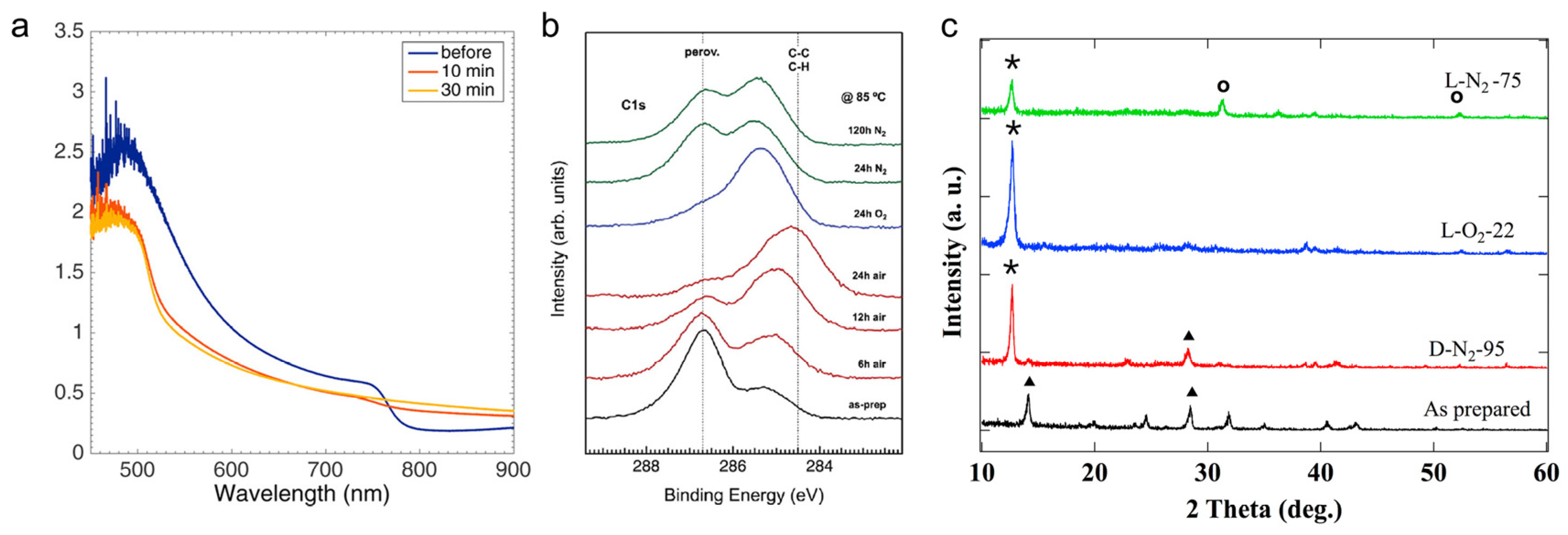
As previously discussed, humidity primarily enhances the decomposition of MHPs. However, MHPs can degrade even in the absence of water due to the inherent thermal instability of certain components. For instance, Beal et al. reported the degradation of MAPbI3 in a noble gas environment. Figure 4a illustrates that MAPbI3 degraded in 10 min at 180°, and the absorption edge of visible light rapidly dropped from 780 nm to 520 nm [75]. Conings et al. further analyzed its degradation mechanism [76]. The binding energy of the C–N bonds in MAI cations was 286.7 eV, and the binding energy of the C–C and C–H bonds was 285.3 eV. XPS measurements (Figure 4b) were obtained over a period of 24 h at 85 °C, revealing a decrease in the peak value of the C–N bonds over time. The increase in the peak value of the C–H bonds indicated the transformation of the bound C in the C–N bonds into amorphous C. Additionally, the decrease in the N1s energy level intensity indicated that N slowly volatilized into the air.
It is evident that temperature alone can induce MHP degradation, albeit at a notably high value of 180 °C, which is not reflective of typical operating conditions. This inconsistency prompted the exploration of additional factors that may interact with temperature to cause MHP degradation at room temperature. To do this, Abdelmageed et al. conducted an experiment to examine the combined effect of temperature and light [77]. MAPbI3 samples were placed in a dark N2 environment at 75°, 85°, and 95°, and their UV–VIS absorbance spectra were recorded. The results align with previous reports, indicating that degradation is more severe at higher temperatures. To study the difference between products degraded by temperature and those degraded by light, Ghada et al. set a dark environment at 95°, a dry air light environment at 30°, and a N2 light environment at 75° and tested them by XRD. Figure 4c shows that the only degradation product in the dark and high-temperature environment was PbI2, but PbI2 and I2 were produced under the simultaneous action of light and temperature. These results indicate that light reduces the temperature required for MHP degradation and alters the degradation pathway induced by temperature. Building upon the volatilization of MAI observed in the aforementioned experiments, Akbulatov et al. investigated the intrinsic thermal decomposition pathways of halogenated perovskites [78]. By utilizing MAPbI3 as an example, thermal decomposition can be summarized into the following two mechanisms:
Temperature also affects phase transition in MHPs. The thermal defects in MHPs are generally vacancy defects and gap defects, also known as intrinsic defects. In polyphase MHPs, different phases correspond to distinct defect state densities. For instance, CsPb(Br0.3I0.7)3 exists in three phases: α, β, and γ. The α phase possesses higher energy compared to the β and γ phases. Consequently, at lower temperatures, CsPb(Br0.3I0.7)3 typically appears in the γ phase. However, upon heating, it undergoes a transformation into the β and α phases. Molecular dynamics analysis indicated that, as the temperature increased, the movement of CsPb(Br0.3I0.7)3 molecules became more vigorous, leading to atom recombination and the activation of vacancy defects and gap defects. Subsequently, these defects induced lattice distortion, ultimately resulting in a phase transition [79].
From a microscopic mechanism perspective, formation energy or dissociation energy is a crucial indicator to characterize the thermal stability of materials. In the case of the MAPbI3 crystal, its poor thermodynamic stability is primarily intrinsic and related to the lower energy cost associated with phase separation compared to other compounds. Remarkably, the dissociation energy of both the cubic and the room-temperature tetragonal phases of MAPbI3 is consistently negative. This implies that the energy required to dissociate or separate these phases into their constituent parts (i.e., the lead iodide (PbI2) and methylammonium iodide (CH3NH3I) components) is lower than the energy gained upon their association. Therefore, under certain heating conditions, the MAPbI3 crystal is prone to phase separation, which will lead to the spontaneous formation of separate domains or clusters of PbI2 and CH3NH3I within the crystal lattice.
2.4. Electric Fields
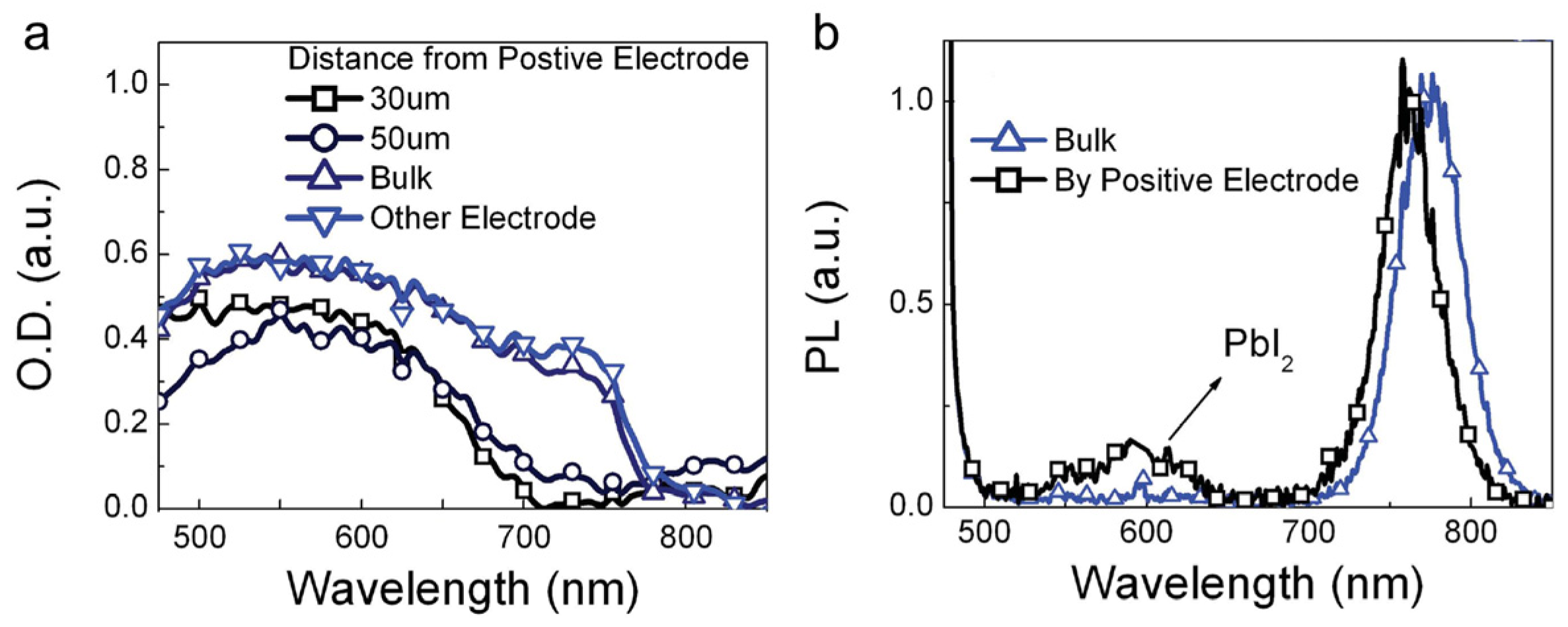
During sensitivity testing of MHPs, it is often observed that the peak value of the signal current decreases after repeated measurements, and the interface topography tends to improve after the tests. These phenomena can be attributed to the induced decomposition effect of electric fields. Antonio et al. found that during the I–V scanning of MHPs, the forward and reverse I–V curves exhibited slight disparities, with the initial scan showing a relatively linear curve. However, subsequent scans revealed a curved I–V diagram, accompanied by a reduction in the measured current. After careful analysis, Rizzo et al. deduced that the prolonged exposure of MHPs to an electric field promotes significant ion migration. As a consequence, ions tend to accumulate in the vicinity of the electrode, inducing slight changes in surface topography. The accumulation of a substantial amount of ions leads to a high ion concentration near the electrode, generating a strong electric field and a high horizontal stress, which contribute to the degradation of the crystal lattice [80].
In a more in-depth study of this phenomenon, Leijtens et al. demonstrated that MAPbI3 decomposed into PbI2, I−, and CH3NH3+ near the electrode (Figure 5) [81]. The role of water in this process has been a subject of inquiry, which was experimentally addressed by Deng et al. [82]. The researchers prepared a pre-wetted sample and a control group for comparison. Under a bias voltage of 0.5 Vμm−1 for 15 min, the pre-wetted sample exhibited a PL (photoluminescence) value decrease of over 70%, while the PL of the control sample remained relatively unchanged. In addition, the PL characteristic peak of PbI2 near 510 nm was also observed, suggesting that the pre-wetted sample had a higher degree of decomposition [82]. The reason is that H2O promotes halogen ion migration, which is consistent with the above results. Deng also explored the relationship between MHP degradation and electric field intensity. They unexpectedly found that the degradation of MHPs was reversible when the electric field was lower than 0.4 V mm−1; when the electric field exceeded 0.4 V mm−1, the PL quenching rate increased, with an increase in bias voltage, and recovery was not achieved. Based on these two experiments, it becomes evident that there exists a threshold value for the combined action of water and electric field. Once the threshold is exceeded, water molecules will participate in the reaction to decompose MHPs, resulting in irreversible changes. However, when the threshold is not surpassed, only the intrinsic effect of the electric field occurs, resulting in ion migration. Water, in this context, only plays a promoting effect and does not cause chemical reactions.
In addition, some researchers have conjectured that the influence of the electric field on perovskite materials extends beyond degradation, with the potential induction of biogenic alterations in perovskite minerals. However, to date, there is a shortage of research in this specific domain [83].
3. Stability Optimization of MHP Detectors
At present, the sensitivity and response time of perovskite detectors have already met the commercial requirements. However, the main obstacle to the widespread commercialization of perovskite detectors is their inherent poor stability. This brief section will outline strategies to improve the stability of these detectors through advancements in molecular design, heterojunction engineering, and doping techniques and improved packaging solutions [84].
3.1. Composition
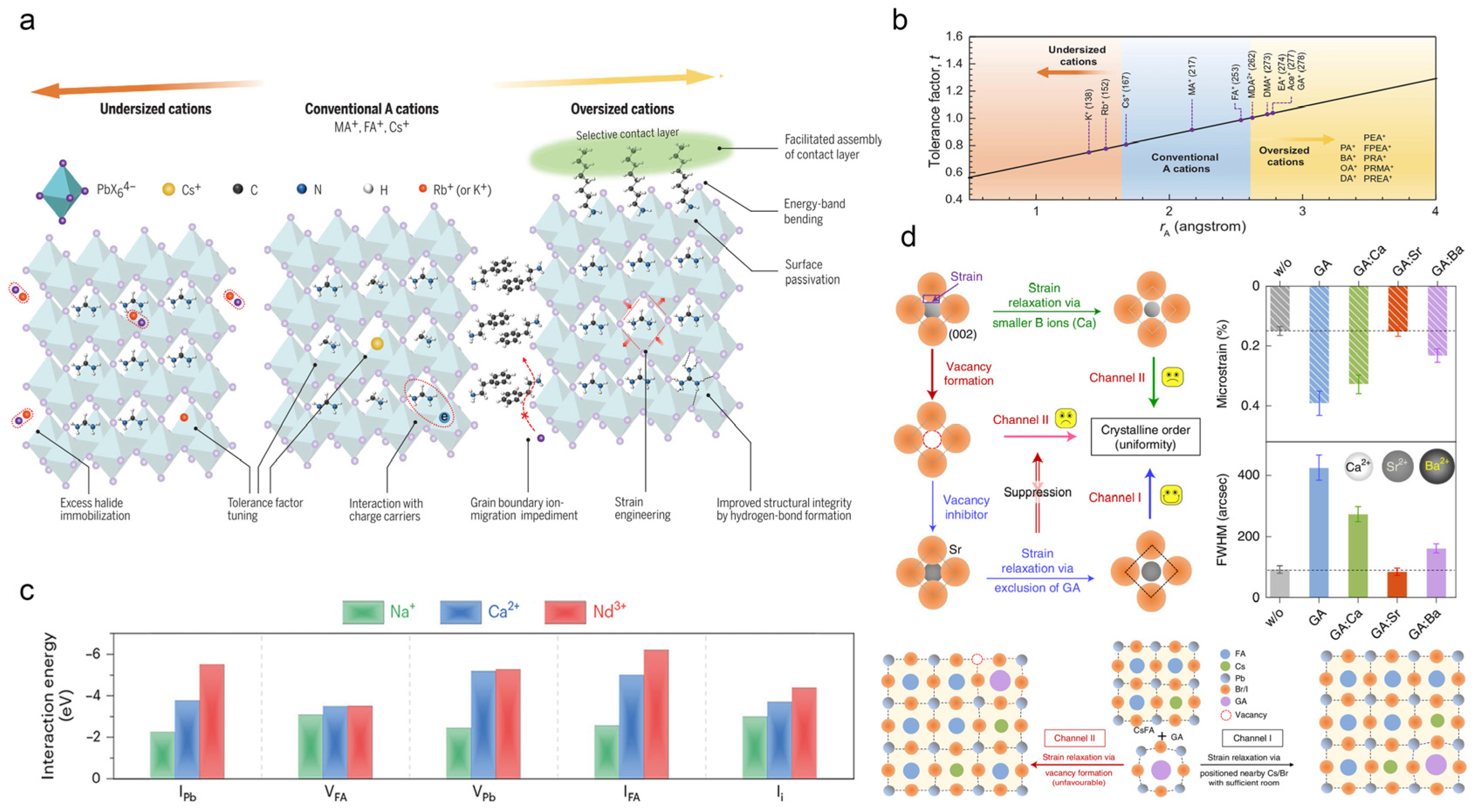
The stability of perovskite is primarily influenced by two main factors: (1) the breaking of ionic bonds and subsequent chemical reactions leading to degradation; (2) the structural changes resulting in phase transformations induced by the provision of energy or external forces. The fundamental solution to address both of these influences lies in improving the structural stability of perovskite materials. In the context of ABX3 perovskites (A is a monovalent cation, B is a divalent metal cation, and X is a halide ion), the structural capability of self-assembled 3D perovskite materials can be predicted using two key parameters: the tolerance factor (t) and the octahedral factor (μ). These factors play a crucial role in determining the stability of the perovskite structure. The prediction formula for assessing structural stability is as follows:
where Rx, RA, and RB are the ionic radii of the X, A, and B ions of the perovskite materials, respectively; μ characterizes the filling of B ions within the X6 octahedron, and t represents the filling of A ions within the BX3 structure. Structural stability is primarily obtained by maintaining a regular octahedral structure, where larger μ and t values indicate higher binding energy. Generally, when the tolerance factor falls within the range of 0.9 ≤ t ≤ 1, a three-dimensional (3D) perovskite structure is formed. On the other hand, when the tolerance factor lies within the range of 0.7 ≤ t ≤ 0.9, the formation of low-dimensional structures such as square and rhombohedral structures can be observed. ABX3 perovskite structures accommodate both inorganic and organic cations at the A-site (Figure 6a). Hydrolysis of ABX3 primarily occurs due to the hydrophilicity of the AX component. By modifying the hydrophilicity of AX, the water stability of the perovskite structure can be significantly improved. Inorganic A-site ions, which include Cs, Rb, K, Li, etc., generally exhibit good stability towards water molecules [85]. For organic A-site ions, methylamine (MA) and formamidine (FA) are commonly used. FA exhibits better humidity stability, due to its larger ionic radius of 2.53 Å, compared to MA, with a radius of 2.17 Å. In the case of MAPbI3 and FAPbI3, the t factor increases from 0.91 to 0.99, indicating higher binding energy (Figure 6b) [86]. In other words, the enhanced stability of halide perovskite materials can be achieved when the radius of the A-site ion closely approaches its critical value. In addition to large-size organic A-site cations, bivalent metal cations like Pb, Sn, and Ge have garnered significant attention due to their excellent photoelectric performance. However, it is worth noting that the bivalent state of Sn and Ge ions is unstable and prone to oxidation into a quadrivalent state. Consequently, the production environment and packaging requirements for Sn- and Ge-based perovskites are more stringent compared to those for Pb-based materials [87].
t = (Rx + RA)/21/2(Rx + RB)
μ = RB/RX
Doping is a technique employed to introduce impurity atoms into a preexisting molecular structure, without altering the original molecular framework. This approach allows for the incorporation of impurity atoms possessing specific characteristics. By doing so, desired attributes such as hydrophobicity and antioxidant properties can be imparted to enhance the stability of the material. In this review, doping is categorized into cationic doping and anionic doping based on the different types of ions used, with the aim of exploring how doping can enhance the stability of perovskite materials. For anionic doping, in the case of ABI3, I− ions are prone to oxidize to elemental I, which significantly compromises the perovskite material stability. For MAPbI3, doping with F− and Cl− is challenging, due to the large difference in ionic radius. However, introducing Br− ions meets the requirements for successful doping. Therefore, the incorporation of bromine ions through ABBrxI(3−x) mixed-halogen perovskite has become the main way to improve the stability of perovskite. Yao et al. [88] provided detailed information on lattice engineering achieved by adding Br ions. This process significantly passivated the defects in the original device and improved certain device performance aspects, promoting carrier migration and mitigating nonradiative recombination effects. Since the strength of the Pb–Br bond is obviously higher than that of the Pb–I bond, bromine doping also contributed to improve the device stability. This was also demonstrated in a comparison between doped and control devices based on FA0.75MA0.25SnI3. Both types of devices were subjected to various stability tests including storage in a N2 environment for 2000 h, continuous exposure to ultraviolet lamps for 300 min, and preservation at approximately 45% air humidity for 40 h. The stability test results clearly showed that the doped device had superior stability [85]. Apart from halogen doping with X elements, the stability of MHPs was also reported to improve through the doping of X elements from Group VI, such as sulfur (S), tellurium (Te), and other similar elements [89].
Apart from doping with halogen anions, an effective strategy to enhance the photoelectric performance and stability of MHPs involves introducing cations of suitable sizes into the interstitial sites of the perovskite structure. These introduced cations can then capture the more mobile X-site species, further improving the overall performance of MHPs. To prevent lattice deformation in MHPs, caused by excessive doping, Zhao et al. compared the effects of neodymium ion (Nd3+) with those of the commonly used sodium ion (Na+) and calcium ion (Ca2+). The results showed that when a small amount of Nd3+ ions was used, the lattice microstrain improved, leading to higher passivation effects (Figure 6c). This suggests that doping with high-valence cations can better inhibit ion migration and enhance material stability [90]. Mixed cations have allowed achieving significant improvements in the stability of perovskite materials.
To achieve a synergistic effect between A and B sites in perovskite materials, Gao et al. introduced specific large organic amine guanidine ions into the A site of ABX3 (Figure 6d). This effectively increased the formation energy of halogen vacancies (X site) through hydrogen bonding. Additionally, low concentrations of alkaline earth metal ion dopants (Sr2+) were incorporated into the B site to raise the formation energy of B site vacancies. By designing and optimizing the device structure, the team achieved exceptional results, with a sensitivity of 2.7 × 10⁴ µCGy−1 cm−2 under a low electric field of 1 V cm−1. The laboratory test showed a stable performance for 5 h and nearly no performance degradation after 180 days of testing [84]. Lien et al. added CsPbI3 to methylamine lead triiodide (CH3NH3PbI3), forming a mixed-cation composition, CH3NH3 (x) Cs (1−x). This approach leveraged the hydrophobic and passivating properties of inorganic cations, effectively enhancing the device performance and improving the overall material stability [91].
Figure 6.
(a) Change of the A-position ion leads to changes in the perovskite material. (b) Taking XPbI3 as an example, tolerance factors correspond to different A-site cation radii [86]. For details, see ref. [86]. Reprinted with permission from ref. [86]. Copyright 2022 Science. (c) Comparison of the passivation effects of Na+, Ca2+, and Nd3+ doped in different perovskites [90]. For details, see ref. [90]. Reprinted with permission from ref. [90]. Copyright 2022 Nat. Mater. (d) Schematic of the doping design of the CsFAG/Sr detector [84]. For details, see ref. [84]. Reprinted with permission from ref. [84]. Copyright 2022 Nat. Photonics.

Essentially, doping involves the introduction of different anion–cation interactions aimed at attracting free ions; typically, doping cations are used to capture free halogen anions. Through the introduction of these strong bonding interactions, the stability of the material is enhanced. However, it is imperative to recognize that doping is typically performed at trace levels. Excessive doping can result in lattice deformation or collapse due to an increase in the lattice microstress, ultimately compromising the stability of the material.
3.2. Heterojunctions
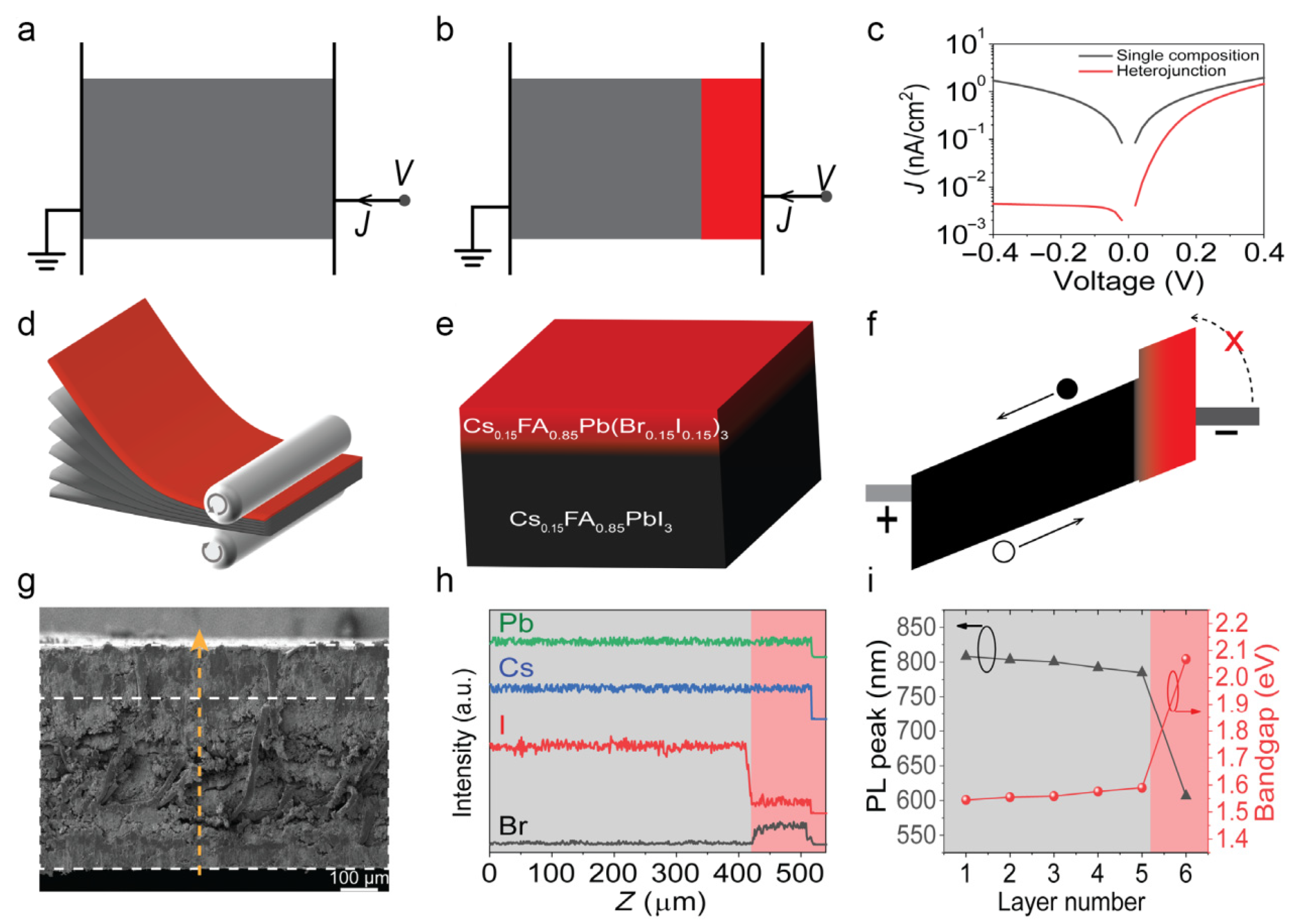
MHPs have emerged as prominent materials for sensitive components in detectors. Specifically, 3D perovskite structures exhibit high sensitivity, a wide dynamic range, and a fast response, which makes them the focus of current research efforts in perovskite detectors development. At present, the sensitivity of perovskite-based X-ray detectors has far exceeded that of the commercial α-Se-based X-ray detector. However, the significant carrier migration in 3D perovskites poses a challenge to achieving commercial-level stability. In this respect, interface engineering through heterojunction and homojunction approaches has shown promising results in improving stability. In particular, heterojunction structures offer the advantage of combining the characteristics of two different semiconductor materials, leading to better complementarity effects compared to homojunction structures. This was demonstrated to effectively reduce noise in large-area and highly sensitive perovskite X-ray detectors (Figure 7a–i) [92].
In the context of detectors, for 3D perovskite materials, which represent the sensitive component of detectors, it is necessary to solve the issues of large noise and high dark current stemming from high ion migration. Two-dimensional perovskite has the characteristic of high resistivity due to its layered structure and large layer spacing caused by large A-site ions. The utilization of wide-gap 2D perovskite materials in detection systems exhibits a deactivation effect that effectively passivates the surface defects present in 3D perovskite structures. By growing a layer of 2D perovskite on the surface of 3D perovskite, a 2D/3D heterojunction is formed, effectively mitigating the dark current and reducing ion migration, thereby enhancing the material stability [93]. It is worth noting that the influence of different types of 2D layers on heterojunction detectors can vary. Specifically, the Dion–Jacobson (DJ) type of 2D layers exhibits better stability compared to the Ruddlesden–Popper (RP) type, owing to the different chemical bonds between the layers. The DJ layer is connected to the 3D perovskite layer through hydrogen bonds, which results in significantly stronger interlayer connections compared to the van der Waals forces characteristic of the RP type. However, the RP perovskite layer containing two A-site cations enables easier charge transfer through the 2D layer, leading to higher sensitivity.
To investigate the impact of different chain lengths on the stability of heterostructures, Kim et al. conducted a study using (FAPbI3)0.95(MAPbBr3)0.05 perovskite films. They examined the effects of different chain lengths of butyl ammonium iodide (BAI), octylammonium iodide (OAI), and dodecyl ammonium iodide (DAI) on the photoelectric properties (PCE) and moisture stability of the materials. The results showed that solar resistance and humidity stability notably increased with the chain length of the 2D layer, from BA to DA [94]. Furthermore, larger A-site ions, such as long-chain alkanes or benzene rings, exhibited enhanced hydrophobicity. However, it is important to note that these ions may also weaken the photoelectric properties of MHPs. Smith and colleagues managed to strike a good balance between photoelectric performance and humidity stability by selecting appropriate A-site ions [95,96].
3.3. Encapsulation
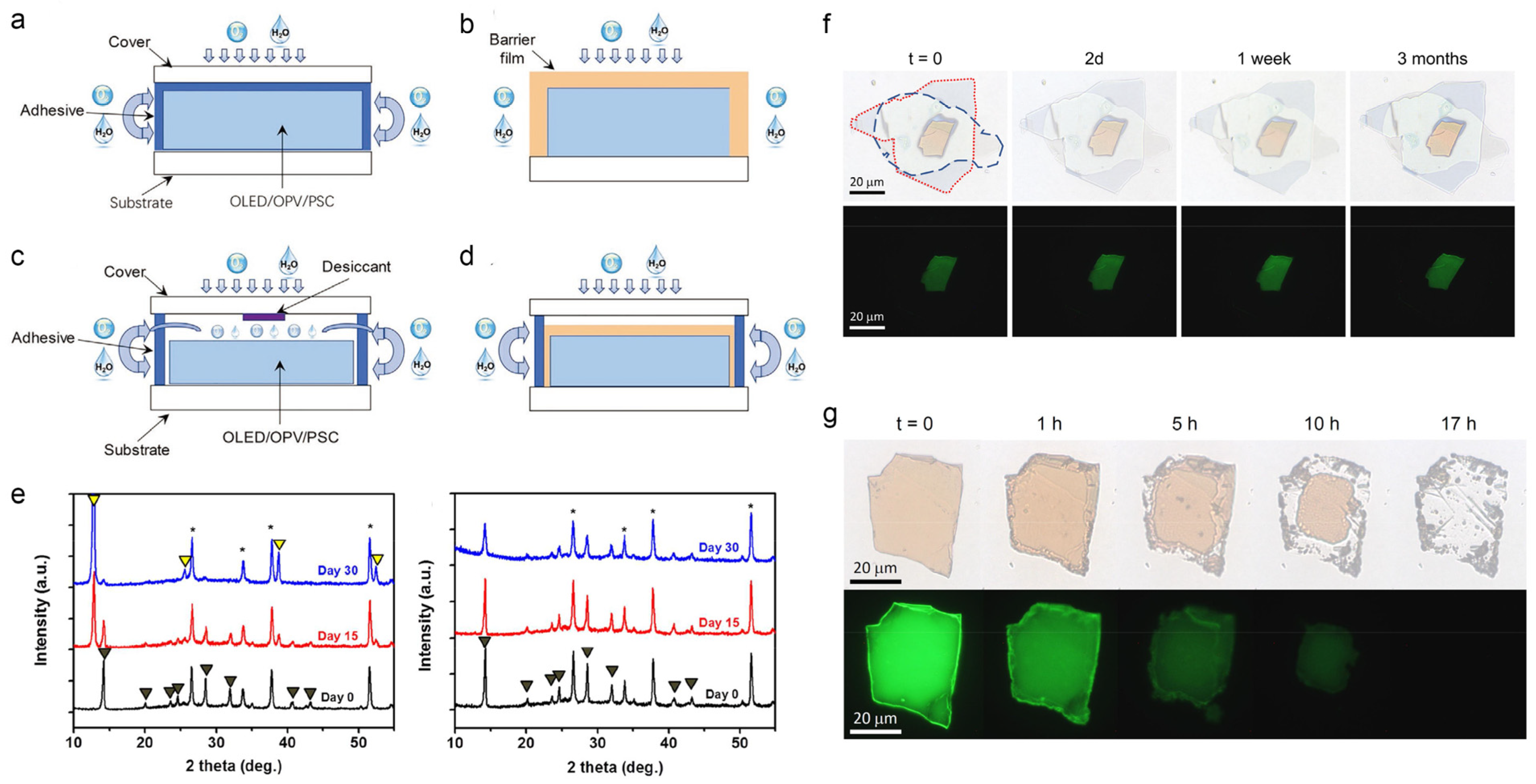
Packaging plays a crucial role in improving the stability of perovskite materials. As early as 2013, Gevorgyan et al. demonstrated the effectiveness of packaging in extending the stability of perovskite devices, successfully storing them for over one year [97]. Here, we will examine the impact of packaging on the stability of materials, focusing on two key aspects: internal packaging and external packaging (Figure 8a–d) [98]. Internal encapsulation involves the application of a film directly onto the surface of the perovskite material to shield it from adverse environmental factors. For proper internal encapsulation in detectors, the film material should exhibit favorable characteristics such as good hydrophobicity, stability, high transmission, low radiation absorption, and compatibility with the perovskite material. Various techniques can be employed to produce thin films, which can be classified into two categories: deposition and coating. With respect to the coating method, using MAPbI3 as the base material, Hwang et al. employed hydrophobic polytetrafluoroethylene (PTFE) as the coating layer to examine the impact of coating on stability. The results clearly showed significant changes in the untreated sample compared to the coated sample. By day 30, the untreated sample had predominantly transformed into PbI2, indicating the occurrence of the aforementioned perovskite hydrolysis reaction. In contrast, the coated experimental sample exhibited minimal changes in color, demonstrating excellent humidity stability. XRD (Figure 8e) and quartz crystal microbalance (QCM) analysis results co-demonstrated that internal encapsulation using a film to cover the perovskite surface effectively created a protective barrier against detrimental environmental factors [99]. Similarly, Li et al. used a hydrophobic polymeric film to enhance the stability of MAPbBr3-based X-ray detectors [100]. In addition to organic polymers, inorganic materials can also be utilized as outer coatings due to their exceptional stability. For instance, Bose et al. employed an AlOx layer to encapsulate MHPs [101], ensuring the long-term stability of the studied device. Similarly, Zhao et al. embedded metal halide scintillators into an array of anodic aluminum oxide (AAO) and compressed them into a film, thereby enhancing the stability of the studied detector [102].
External packaging involves the use of materials such as glass to create a closed environment around the perovskite material, effectively protecting it from water and oxygen in the external surroundings. In addition to providing a barrier against water and air, certain external packaging materials like silica gel possess soft characteristics that offer collision buffering. Currently, the most commonly employed external packaging method is glass–glass packaging. This involves placing the perovskite material between glass layers, evacuating the air (preferably in an inert gas atmosphere), and sealing the edges using materials such as ethylene vinyl acetate copolymer (EVA) and polyisobutylene (PIB) [103]. In addition to glass–glass packaging, other organic and inorganic materials have been explored for external packaging. Yang et al. utilized hexagonal boron nitride (hBN) to package perovskite, significantly extending the stable preservation time of MHPs from 30 min to 10 h under intense light conditions [104]. Seitz et al. developed a double-sided package (hBN/perovskite/hBN) that completely enclosed perovskite flakes within hBN layers, resulting in a storage time extension from 5 h to 3 months, without significant degradation (Figure 8f,g) [105].
Figure 8.
(a–d) The schematics of different encapsulation methods are as follows: edged-cover encapsulation, film encapsulation, full-cover encapsulation, hybrid encapsulation [98]. For details, see ref. [98]. Reprinted with permission from ref. [98]. Copyright 2021 Adv. Funct. Mater. (e) Changed XRD patterns for the MAPbI3 control group and the experimental group (coated with polytetrafluoroethylene) (*, peaks from FTO; yellow mark, peaks from PbI2; dark brown marks, peaks from perovskite) [99]. For details, see ref. [99]. Reprinted with permission from ref. [99]. Copyright 2015 ACS Appl. Mater. Inter. (f,g) Comparison of the transmission and fluorescence micrographs of perovskite flakes (The dashed blue and red lines represent the bottom and top edges of the hBN, respectively); (g) control group, (f) encapsulation group [105]. For details, see ref. [105]. Reprinted with permission from ref. [105]. Copyright 2019 Nanomaterials.

4. Conclusions and Outlook
In conclusion, this review provides a comprehensive exploration of the chemical stability of halide perovskite detectors, focusing on the influence of various external factors. The findings highlight the critical importance of addressing the challenges associated with long-term stability to unlock the full potential of MHP detectors for practical applications in sensing and imaging.
Radiation, humidity, temperature, and electric field were identified as key factors that significantly impact the stability of MHP detectors. Through the uptake of moisture, perovskite materials undergo degradation processes leading to the formation of undesirable byproducts and the degradation of device performance. Similarly, exposure to elevated temperatures, electric fields, and radiation can induce structural defects and affect the integrity of the MHP material.
To mitigate the adverse effects of environmental factors and devise effective strategies for enhancing the chemical stability of halide perovskite detectors, extensive research has been conducted. Composition engineering, heterostructure construction, and encapsulation have emerged as promising approaches for protecting perovskite materials from moisture-induced degradation and other environmental threats. Additionally, the incorporation of protective layers, such as hydrophobic coatings or barrier films, has shown potential in preventing water diffusion and improving the stability of halide perovskite detectors. Furthermore, it is imperative to make further advancements in order to address the remaining challenges and enhance the long-term stability of halide perovskite detectors. Developing comprehensive models that can accurately predict and comprehend the intricate interplay between environmental factors and perovskite materials is of utmost importance. These models will serve as essential tools for guiding future research and engineering endeavors in this field. Additionally, novel materials with enhanced stability, such as doped, mixed-halide, or double-perovskite structures, hold promise for achieving improved chemical stability under diverse operating conditions. Moreover, advancements in fabrication techniques, such as scalable deposition methods and improved encapsulation technologies, are essential for enabling the large-scale production of stable halide perovskite detectors.
The significance of the aforementioned stability factors and their combined effects may vary for different types of detectors. Taking X-ray detectors as an example, the areas in which they are most commonly employed are computed tomography (CT) and industrial flaw detection. These applications typically involve minimal temperature fluctuations and relatively low electric fields, thereby reducing the impact of these two factors. However, the influence of humidity, oxygen, and radiation becomes magnified in such scenarios. In the medical field, it is crucial to minimize the amount of X-ray exposure for patient safety, and due to the stringent standards required by the industry, the sensitivity and stability of the detector are of utmost importance. Encapsulation can potentially mitigate the effects of humidity and oxygen by preventing contact with the detector material. But high-energy X-rays can readily induce both phase separation and decomposition. Consequently, for X-ray detector materials, the strength of the ionic bonds becomes particularly crucial to maintain long-term stability under irradiation. This emphasizes the need for further in-depth research into the bonding or atomic structure of MHPs for X-ray detectors. For most other detectors (such as infrared detectors, photodetectors, ultraviolet detectors, etc.), the primary concerns regard the effects of humidity and oxygen. The current solutions involving heterojunctions, encapsulation, or doping have shown promising results in addressing these challenges.
Furthermore, efforts should be directed towards standardizing testing protocols and evaluation metrics for assessing the stability of these detectors, including continuous working time, long-term stability, and radiation dose tolerance, enabling robust comparisons and accelerated progress in this field.
Ultimately, improving the chemical stability of MHP detectors will facilitate their integration into industrial applications, such as environmental monitoring, biomedical imaging, and security systems. With continued research and technological advancements, MHP detectors have the potential to revolutionize the field of detectors, offering high performance, cost-effectiveness, and stability for a wide range of applications. We believe that this review will serve as a valuable resource and as a catalyst for further advancements to achieve the desired long-term stability of MHP detectors.
Author Contributions
Conceptualization, B.X. and B.Z.; Writing—original draft preparation, S.X., B.X. and B.Z.; Writing—review and editing, X.W. and S.X.; supervision, X.W. and S.X.; funding acquisition, X.W. and S.X. All authors have read and agreed to the published version of the manuscript.
Funding
This research was funded by the National Natural Science Foundation of China (22261160370 and 21905006), the Natural Science Foundation of Hunan Province, China (2023JJ50132), the Guangdong Provincial Science and Technology Plan (2021A0505110003), the Guangdong Basic and Applied Basic Research Foundation (2020B1515120039), the Shenzhen Science and Technology Program (JCYJ20220818100211025, ZDSYS20200811143600001 and 2022378670), and the Natural Science Foundation of Top Talent of SZTU (GDRC202343).
Data Availability Statement
Not applicable.
Conflicts of Interest
The authors declare no conflicts of interest.
References
- Corti, M.; Bonomi, S.; Chiara, R.; Romani, L.; Quadrelli, P.; Malavasi, L. Application of metal halide perovskites as photocatalysts in organic reactions. Inorganics 2021, 9, 56. [Google Scholar] [CrossRef]
- Xiao, S.; Qian, W.; Yang, S. Interfaced structures between halide perovskites: From basics to construction to optoelectronic applications. Adv. Energy Mater. 2023, 13, 2201472. [Google Scholar] [CrossRef]
- Xu, F.; Zou, Y.; Dai, Y.; Li, M.; Li, Z. Halide perovskites and high-pressure technologies: A fruitful encounter. Mater. Chem. Front. 2023, 7, 2102–2119. [Google Scholar] [CrossRef]
- Deng, Y.; Liu, H.; Wang, H.; Song, Y.; Li, W.; Zhu, L.; Xie, X.; Xiao, S.; Chen, H. Carbon-based Sb2 (S, Se)3 solar cells. Inorganics 2023, 11, 159. [Google Scholar] [CrossRef]
- Wei, X.; Zhang, P.; Xu, T.; Zhou, H.; Bai, Y.; Chen, Q. Chemical approaches for electronic doping in photovoltaic materials beyond crystalline silicon. Chem. Soc. Rev. 2022, 51, 10016–10063. [Google Scholar] [CrossRef]
- Bu, H.; He, C.; Xu, Y.; Xing, L.; Liu, X.; Ren, S.; Yi, S.; Chen, L.; Wu, H.; Zhang, G.; et al. Emerging new-generation detecting and sensing of metal halide perovskites. Adv. Electron. Mater. 2022, 8, 2101204. [Google Scholar] [CrossRef]
- He, Y.; Hadar, I.; Kanatzidis, M.G. Detecting ionizing radiation using halide perovskite semiconductors processed through solution and alternative methods. Nat. Photonics 2022, 16, 14–26. [Google Scholar] [CrossRef]
- Stoumpos, C.C.; Malliakas, C.D.; Kanatzidis, M.G. Semiconducting tin and lead iodide perovskites with organic cations: Phase transitions, high mobilities, and near-infrared photoluminescent properties. Inorg. Chem. 2013, 52, 9019–9038. [Google Scholar] [CrossRef]
- Dong, Q.; Fang, Y.; Shao, Y.; Mulligan, P.; Qiu, J.; Cao, L.; Huang, J. Electron-hole diffusion lengths > 175 μm in solution-grown CH3NH3PbI3 single crystals. Science 2015, 347, 967–970. [Google Scholar] [CrossRef]
- Rajagopal, A.; Yang, Z.; Jo, S.B.; Braly, I.L.; Liang, P.W.; Hillhouse, H.W.; Jen, A.K.Y. Highly efficient perovskite–perovskite tandem solar cells reaching 80% of the theoretical limit in photovoltage. Adv. Mater. 2017, 29, 1702140. [Google Scholar] [CrossRef]
- Jacak, J.E.; Jacak, W.A. Routes for metallization of perovskite solar cells. Materials 2022, 15, 2254. [Google Scholar] [CrossRef] [PubMed]
- Li, H.; Shen, N.; Chen, S.; Guo, F.; Xu, B. Recent progress on synthesis, intrinsic properties and optoelectronic applications of perovskite single crystals. Adv. Funct. Mater. 2023, 33, 2214339. [Google Scholar] [CrossRef]
- Bao, C.; Xu, W.; Yang, J.; Bai, S.; Teng, P.; Yang, Y.; Wang, J.; Zhao, N.; Zhang, W.; Huang, W.; et al. Bidirectional optical signal transmission between two identical devices using perovskite diodes. Nat. Electron. 2020, 3, 156–164. [Google Scholar] [CrossRef] [PubMed]
- He, X.; Deng, Y.; Ouyang, D.; Zhang, N.; Wang, J.; Murthy, A.A.; Spanopoulos, I.; Islam, S.M.; Tu, Q.; Xing, G.; et al. Recent development of halide perovskite materials and devices for ionizing radiation detection. Chem. Rev. 2023, 123, 1207–1261. [Google Scholar] [CrossRef] [PubMed]
- Dudipala, K.R.; Le, T.-H.; Nie, W.; Hoye, R.L.Z. Halide perovskites and their derivatives for efficient, high-resolution direct radiation detection: Design strategies and applications. Adv. Mater. 2023, 35, 2304523. [Google Scholar] [CrossRef] [PubMed]
- Zhou, F.; Li, Z.; Lan, W.; Wang, Q.; Ding, L.; Jin, Z. Halide perovskite, a potential scintillator for x-ray detection. Small Methods 2020, 4, 2000506. [Google Scholar] [CrossRef]
- Wang, Y.; Li, M.; Chai, Z.; Wang, Y.; Wang, S. Perovskite scintillators for improved X-ray detection and imaging. Angew. Chem. Int. Edit. 2023, 62, e202304638. [Google Scholar] [CrossRef]
- He, Y.; Lin, Z.; Wang, J.; Zhang, K.; Xu, X.; Li, Y.; Huang, X.; Ma, T.; Xiao, S.; Yang, S. A heat-liquefiable solid precursor for ambient growth of perovskites with high tunability, performance and stability. Small Methods 2022, 6, 2200384. [Google Scholar] [CrossRef]
- Hu, H.; Niu, G.; Zheng, Z.; Xu, L.; Liu, L.; Tang, J. Perovskite semiconductors for ionizing radiation detection. EcoMat 2022, 4, e12258. [Google Scholar] [CrossRef]
- Boyd, C.C.; Cheacharoen, R.; Leijtens, T.; McGehee, M.D. Understanding degradation mechanisms and improving stability of perovskite photovoltaics. Chem. Rev. 2019, 119, 3418–3451. [Google Scholar] [CrossRef] [PubMed]
- Dunfield, S.P.; Bliss, L.; Zhang, F.; Luther, J.M.; Zhu, K.; van Hest, M.F.A.M.; Reese, M.O.; Berry, J.J. From defects to degradation: A mechanistic understanding of degradation in perovskite solar cell devices and modules. Adv. Energy Mater. 2020, 10, 1904054. [Google Scholar] [CrossRef]
- Meng, X.; Tian, X.; Zhang, S.; Zhou, J.; Zhang, Y.; Liu, Z.; Chen, W. In situ characterization for understanding the degradation in perovskite solar cells. Sol. RRL 2022, 6, 2200772. [Google Scholar] [CrossRef]
- Aristidou, N.; Sanchez-Molina, I.; Chotchuangchutchaval, T.; Brown, M.; Martinez, L.; Rath, T.; Haque, S.A. The role of oxygen in the degradation of methylammonium lead trihalide perovskite photoactive layers. Angew. Chem. Int. Ed. 2015, 54, 8208–8212. [Google Scholar] [CrossRef]
- Nickel, N.H.; Lang, F.; Brus, V.V.; Shargaieva, O.; Rappich, J. Unraveling the light-induced degradation mechanisms of CH3NH3PbI3 perovskite films. Adv. Electron. Mater. 2017, 3, 1700158. [Google Scholar] [CrossRef]
- Gottesman, R.; Gouda, L.; Kalanoor, B.S.; Haltzi, E.; Tirosh, S.; Rosh-Hodesh, E.; Tischler, Y.; Zaban, A.; Quarti, C.; Mosconi, E.; et al. Photoinduced reversible structural transformations in free-standing CH3NH3PbI3 perovskite films. J. Phys. Chem. Lett. 2015, 6, 2332–2338. [Google Scholar] [CrossRef]
- Nie, W.; Blancon, J.-C.; Neukirch, A.J.; Appavoo, K.; Tsai, H.; Chhowalla, M.; Alam, M.A.; Sfeir, M.Y.; Katan, C.; Even, J.; et al. Light-activated photocurrent degradation and self-healing in perovskite solar cells. Nat. Commun. 2016, 7, 11574. [Google Scholar] [CrossRef]
- Domanski, K.; Roose, B.; Matsui, T.; Saliba, M.; Turren-Cruz, S.-H.; Correa-Baena, J.-P.; Roldan-Carmona, C.; Richardson, G.; Foster, J.M.; De Angelis, F.; et al. Migration of cations induces reversible performance losses over day/night cycling in perovskite solar cells. Energy Environ. Sci. 2017, 10, 604–613. [Google Scholar] [CrossRef]
- Yang, X.; Yan, X.; Wang, W.; Zhu, X.; Li, H.; Ma, W.; Sheng, C. Light induced metastable modification of optical properties in CH3NH3PbI3− xBrx perovskite films: Two-step mechanism. Org. Electron. 2016, 34, 79–83. [Google Scholar] [CrossRef]
- Kirschner, M.S.; Diroll, B.T.; Guo, P.; Haryey, S.M.; Helweh, W.; Flanders, N.C.; Brumberg, A.; Watkins, N.E.; Leonard, A.A.; Evans, A.M.; et al. Photoinduced, reversible phase transitions in all-inorganic perovskite nanocrystals. Nat. Commun. 2019, 10, 504. [Google Scholar] [CrossRef] [PubMed]
- Zhou, Y.; You, L.; Wang, S.; Ku, Z.; Fan, H.; Schmidt, D.; Rusydi, A.; Chang, L.; Wang, L.; Ren, P.; et al. Giant photostriction in organic-inorganic lead halide perovskites. Nat. Commun. 2016, 7, 11193. [Google Scholar] [CrossRef] [PubMed]
- Conings, B.; Baeten, L.; De Dobbelaere, C.; D’Haen, J.; Manca, J.; Boyen, H.-G. Perovskite-based hybrid solar cells exceeding 10% efficiency with high reproducibility using a thin film sandwich approach. Adv. Mater. 2014, 26, 2041–2046. [Google Scholar] [CrossRef]
- Shkrob, I.A.; Marin, T.W. Charge trapping in photovoltaically active perovskites and related halogenoplumbate compounds. J. Phys. Chem. Lett. 2014, 5, 1066–1071. [Google Scholar] [CrossRef]
- Philippe, B.; Park, B.-W.; Lindblad, R.; Oscarsson, J.; Ahmadi, S.; Johansson, E.M.J.; Rensmo, H. Chemical and electronic structure characterization of lead halide perovskites and stability behavior under different exposures—A photoelectron spectroscopy investigation. Chem. Mater. 2015, 27, 1720–1731. [Google Scholar] [CrossRef]
- Lin, W.-C.; Lo, W.-C.; Li, J.-X.; Wang, Y.-K.; Tang, J.-F.; Fong, Z.-Y. In situ XPS investigation of the X-ray-triggered decomposition of perovskites in ultrahigh vacuum condition. NPJ Mat. Degrad. 2021, 5, 13. [Google Scholar] [CrossRef]
- Svanstrom, S.; Garcia Fernandez, A.; Sloboda, T.; Jacobsson, T.J.; Rensmo, H.; Cappel, U.B. X-ray stability and degradation mechanism of lead halide perovskites and lead halides. Phys. Chem. Chem. Phys. 2021, 23, 12479–12489. [Google Scholar] [CrossRef] [PubMed]
- Dai, X.; Fei, C.; Kandlakunta, P.; Zhao, L.; Ni, Z.; Cao, L.R.; Huang, J. Origin of the X-ray-induced damage in perovskite solar cells. IEEE Trans. Nucl. Sci. 2022, 69, 1850–1856. [Google Scholar] [CrossRef]
- Motoki, K.; Miyazawa, Y.; Kobayashi, D.; Ikegami, M.; Miyasaka, T.; Yamamoto, T.; Hirose, K. Degradation of CH3NH3PbI3 perovskite due to soft X-ray irradiation as analyzed by an X-ray photoelectron spectroscopy time-dependent measurement method. J. Appl. Phys. 2017, 121, 085501. [Google Scholar] [CrossRef]
- Armaroli, G.; Ferlauto, L.; Ledee, F.; Lini, M.; Ciavatti, A.; Kovtun, A.; Borgatti, F.; Calabrese, G.; Milita, S.; Fraboni, B.; et al. X-ray-induced modification of the photophysical properties of MAPbBr3 single crystals. ACS Appl. Mater. Interfaces 2021, 13, 58301–58308. [Google Scholar] [CrossRef] [PubMed]
- Wang, C.; Ecker, B.R.; Wei, H.; Huang, J.; Gao, Y. Environmental surface stability of the MAPbBr3 single crystal. J. Phys. Chem. C 2018, 122, 3513–3522. [Google Scholar] [CrossRef]
- Garcia-Fernandez, A.; Kammlander, B.; Riva, S.; Rensmo, H.; Cappel, U.B. Composition dependence of X-ray stability and degradation mechanisms at lead halide perovskite single crystal surfaces. Phys. Chem. Chem. Phys. 2024, 26, 1000–1010. [Google Scholar] [CrossRef]
- Yang, S.; Xu, Z.; Xue, S.; Kandlakunta, P.; Cao, L.; Huang, J. Organohalide lead perovskites: More stable than glass undergamma-ray radiation. Adv. Mater. 2019, 31, 0935–9648. [Google Scholar] [CrossRef]
- Boldyreva, A.G.; Akbulatov, A.F.; Tsarev, S.A.; Luchkin, S.Y.; Zhidkov, I.S.; Kurmaev, E.Z.; Stevenson, K.J.; Petrov, V.G.; Troshin, P.A. Γ-ray-induced degradation in the triple-cation perovskite solar cells. J. Phys. Chem. Lett. 2019, 10, 813–818. [Google Scholar] [CrossRef]
- Yang, K.; Huang, K.; Li, X.; Zheng, S.; Hou, P.; Wang, J.; Guo, H.; Song, H.; Li, B.; Li, H.; et al. Radiation tolerance of perovskite solar cells under gamma ray. Org. Electron. 2019, 71, 79–84. [Google Scholar] [CrossRef]
- Boldyreva, A.G.; Frolova, L.A.; Zhidkov, I.S.; Gutsev, L.G.; Kurmaev, E.Z.; Ramachandran, B.R.; Petrov, V.G.; Stevenson, K.J.; Aldoshin, S.M.; Troshin, P.A. Unravelling the material composition effects on the gamma ray stability of lead halide perovskite solar cells: MAPbI3 breaks the records. J. Phys. Chem. Lett. 2020, 11, 2630–2636. [Google Scholar] [CrossRef]
- Xu, Q.; Zhang, H.; Nie, J.; Shao, W.; Wang, X.; Zhang, B.; Ouyang, X. Effect of methylammonium lead tribromide perovskite based-photoconductor under gamma photons radiation. Radiat. Phys. Chem. 2021, 181, 109337. [Google Scholar] [CrossRef]
- Gao, L.; Tao, K.; Sun, J.-L.; Yan, Q. Gamma-ray radiation stability of mixed-cation lead mixed-halide perovskite single crystals. Adv. Opt. Mater. 2022, 10, 2102069. [Google Scholar] [CrossRef]
- Gao, L.; Sun, J.-L.; Li, Q.; Yan, Q. γ-ray radiation hardness of CsPbBr3 single crystals and single-carrier devices. ACS Appl. Mater. Interfaces 2022, 14, 37904–37915. [Google Scholar] [CrossRef]
- De Siena, M.C.; Klepov, V.V.; Stepanoff, S.P.; Bayikadi, K.S.; Pan, L.; Pandey, I.R.; Karki, S.; Chung, D.Y.; Wolfe, D.E.; Kanatzidis, M.G. Extreme γ-ray radiation tolerance of spectrometer-grade CsPbBr3 perovskite detectors. Adv. Mater. 2023, 35, 2303244. [Google Scholar] [CrossRef]
- Zaffalon, M.L.; Cova, F.; Liu, M.; Cemmi, A.; Di Sarcina, I.; Rossi, F.; Carulli, F.; Erroi, A.; Roda, C.; Perego, J.; et al. Extreme γ-ray radiation hardness and high scintillation yield in perovskite nanocrystals. Nat. Photonics 2022, 16, 860–868. [Google Scholar] [CrossRef]
- Gao, L.; Li, Q.; Sun, J.-L.; Yan, Q. Gamma-ray irradiation stability of zero-dimensional cs3cu2i5 metal halide scintillator single crystals. J. Phys. Chem. Lett. 2023, 14, 1165–1173. [Google Scholar] [CrossRef]
- Ozerova, V.V.; Emelianov, N.A.; Kiryukhin, D.P.; Kushch, P.P.; Shilov, G.V.; Kichigina, G.A.; Aldoshin, S.M.; Frolova, L.A.; Troshin, P.A. Exploring the limits: Degradation behavior of lead halide perovskite films under exposure to ultrahigh doses of γ rays of up to 10 MGy. J. Phys. Chem. Lett. 2023, 14, 743–749. [Google Scholar] [CrossRef] [PubMed]
- Dang, Z.; Shamsi, J.; Palazon, F.; Imran, M.; Akkerman, Q.A.; Park, S.; Bertoni, G.; Prato, M.; Brescia, R.; Manna, L. In situ transmission electron microscopy study of electron beam-induced transformations in colloidal cesium lead halide perovskite nanocrystals. ACS Nano 2017, 11, 2124–2132. [Google Scholar] [CrossRef] [PubMed]
- Chen, X.; Wang, Z. Investigating chemical and structural instabilities of lead halide perovskite induced by electron beam irradiation. Micron 2019, 116, 73–79. [Google Scholar] [CrossRef] [PubMed]
- Syafutra, H.; Yun, J.-H.; Yoshie, Y.; Lyu, M.; Takeda, S.N.; Nakamura, M.; Wang, L.; Jung, M.-C. Surface degradation mechanism on CH3NH3PbBr3 hybrid perovskite single crystal by a grazing e-beam irradiation. Nanomaterials 2020, 10, 1253. [Google Scholar] [CrossRef] [PubMed]
- Huang, J.-S.; Kelzenberg, M.D.; Espinet-Gonzalez, P.; Mann, C.; Walker, D.; Naqavi, A.; Vaidya, N.; Warmann, E.; Atwater, H.A. Effects of electron and proton radiation on perovskite solar cells for space solar power application. In Proceedings of the IEEE 44th Photovoltaic Specialist Conference (PVSC), Washington, DC, USA, 25–30 June 2017; pp. 1248–1252. [Google Scholar]
- Miyazawa, Y.; Kim, G.M.; Ishii, A.; Ikegami, M.; Miyasaka, T.; Suzuki, Y.; Yamamoto, T.; Ohshima, T.; Kanaya, S.; Toyota, H.; et al. Evaluation of damage coefficient for minority-carrier diffusion length of triple-cation perovskite solar cells under 1 mev electron irradiation for space applications. J. Phys. Chem. C 2021, 125, 13131–13137. [Google Scholar] [CrossRef]
- Lang, F.; Nickel, N.H.; Bundesmann, J.; Seidel, S.; Denker, A.; Albrecht, S.; Brus, V.V.; Rappich, J.; Rech, B.; Landi, G.; et al. Radiation hardness and self-healing of perovskite solar cells. Adv. Mater. 2016, 28, 8726–8731. [Google Scholar] [CrossRef]
- Miyazawa, Y.; Ikegami, M.; Chen, H.-W.; Ohshima, T.; Imaizumi, M.; Hirose, K.; Miyasaka, T. Tolerance of perovskite solar cell to high-energy particle irradiations in space environment. iScience 2018, 2, 148–155. [Google Scholar] [CrossRef]
- Afshari, H.; Chacon, S.A.; Durant, B.K.; Crawford, R.; Rout, B.; Eperon, G.E.; Sellers, I.R. Radiation tolerance, high temperature stability, and self-healing of triple halide perovskite solar cells. In Proceedings of the IEEE 49th Photovoltaics Specialists Conference (PVSC), Philadelphia, PA, USA, 5–10 June 2022; p. 836. [Google Scholar]
- Huang, H.; Guo, L.; Zhao, Y.; Peng, S.; Ma, W.; Wang, X.; Xue, J. Radiation-tolerant proton detector based on the mapbbr3 single crystal. ACS Appl. Electron. Mater. 2023, 5, 381–387. [Google Scholar] [CrossRef]
- Paterno, G.M.; Robbiano, V.; Santarelli, L.; Zampetti, A.; Cazzaniga, C.; Sakai, V.G.; Cacialli, F. Perovskite solar cell resilience to fast neutrons. Sustain. Energy Fuels 2019, 3, 2561–2566. [Google Scholar] [CrossRef]
- De Rossi, F.; Taheri, B.; Bonomo, M.; Gupta, V.; Renno, G.; Nia, N.Y.; Rech, P.; Frost, C.; Cazzaniga, C.; Quagliotto, P.; et al. Neutron irradiated perovskite films and solar cells on pet substrates. Nano Energy 2022, 93, 106879. [Google Scholar] [CrossRef]
- Rafiei Rad, R.; Azizollah Ganji, B.; Taghavinia, N. 4-tert-butyl pyridine additive for moisture-resistant wide bandgap perovskite solar cells. Opt. Mater. 2022, 123, 111876. [Google Scholar] [CrossRef]
- Strachala, D.; Hylsky, J.; Vanek, J. Influence of moisture on perovskite photovoltaic cells. ECS Trans. 2017, 81, 191–198. [Google Scholar] [CrossRef]
- Xiang, W.; Liu, S.; Tress, W. A review on the stability of inorganic metal halide perovskites: Challenges and opportunities for stable solar cells. Energy Environ. Sci. 2021, 14, 2090–2113. [Google Scholar] [CrossRef]
- Sun, K.; Mueller-Buschbaum, P. Shedding light on the moisture stability of halide perovskite thin films. Energy Technol. 2023, 11, 2201475. [Google Scholar] [CrossRef]
- Hsu, R.-Y.; Liang, Y.-J.; Hung, Y.-J.; Lin, Y.-C. Impact of humidity in triple cation perovskite solar cells: Surface analysis. Mat. Sci. Semicon. Proc. 2022, 152, 107100. [Google Scholar] [CrossRef]
- Ho, K.; Wei, M.; Sargent, E.H.; Walker, G.C. Grain transformation and degradation mechanism of formamidinium and cesium lead iodide perovskite under humidity and light. ACS Energy Lett. 2021, 6, 934–940. [Google Scholar] [CrossRef]
- Wang, Q.; Chen, B.; Liu, Y.; Deng, Y.; Bai, Y.; Dong, Q.; Huang, J. Scaling behavior of moisture-induced grain degradation in polycrystalline hybrid perovskite thin films. Energy Environ. Sci. 2017, 10, 516–522. [Google Scholar] [CrossRef]
- Niu, G.; Li, W.; Meng, F.; Wang, L.; Dong, H.; Qiu, Y. Study on the stability of CH3NH3PbI3 films and the effect of post-modification by aluminum oxide in all-solid-state hybrid solar cells. J. Phys. Chem. A 2014, 2, 705–710. [Google Scholar]
- Fan, Z.; Xiao, H.; Wang, Y.; Zhao, Z.; Lin, Z.; Cheng, H.-C.; Lee, S.-J.; Wang, G.; Feng, Z.; Goddard, W.A., III; et al. Layer-by-layer degradation of methylammonium lead tri-iodide perovskite microplates. Joule 2017, 1, 548–562. [Google Scholar] [CrossRef]
- Howard, J.M.; Tennyson, E.M.; Barik, S.; Szostak, R.; Waks, E.; Toney, M.F.; Nogueira, A.F.; Neves, B.R.A.; Leite, M.S. Humidity-induced photoluminescence hysteresis in variable Cs/Br ratio hybrid perovskites. J. Phys. Chem. Lett. 2018, 9, 3463–3469. [Google Scholar] [CrossRef]
- Zheng, C.; Rubel, O. Unraveling the water degradation mechanism of CH3NH3PbI3. J. Phys. Chem. C 2019, 123, 19385–19394. [Google Scholar] [CrossRef]
- Dastidar, S.; Egger, D.A.; Tan, L.Z.; Cromer, S.B.; Dillon, A.D.; Liu, S.; Kronik, L.; Rappe, A.M.; Fafarman, A.T. High chloride doping levels stabilize the perovskite phase of cesium lead iodide. Nano Lett. 2016, 16, 3563–3570. [Google Scholar] [CrossRef] [PubMed]
- Beal, R.E.; Slotcavage, D.J.; Leijtens, T.; Bowring, A.R.; Belisle, R.A.; Nguyen, W.H.; Burkhard, G.F.; Hoke, E.T.; McGehee, M.D. Cesium lead halide perovskites with improved stability for tandem solar cells. J. Phys. Chem. Lett. 2016, 7, 746–751. [Google Scholar] [CrossRef] [PubMed]
- Conings, B.; Drijkoningen, J.; Gauquelin, N.; Babayigit, A.; D’Haen, J.; D’Olieslaeger, L.; Ethirajan, A.; Verbeeck, J.; Manca, J.; Mosconi, E.; et al. Intrinsic thermal instability of methylammonium lead trihalide perovskite. Adv. Energy Mater. 2015, 5, 1500477. [Google Scholar] [CrossRef]
- Abdelmageed, G.; Mackeen, C.; Hellier, K.; Jewell, L.; Seymour, L.; Tingwald, M.; Bridges, F.; Zhang, J.Z.; Carter, S. Effect of temperature on light induced degradation in methylammonium lead iodide perovskite thin films and solar cells. Sol. Energy Mater. Sol. Cells 2018, 174, 566–571. [Google Scholar] [CrossRef]
- Akbulatov, A.F.; Martynenko, V.M.; Frolova, L.A.; Dremova, N.N.; Zhidkov, I.; Tsarev, S.A.; Luchkin, S.Y.; Kurmaev, E.Z.; Aldoshin, S.M.; Stevenson, K.J.; et al. Intrinsic thermal decomposition pathways of lead halide perovskites APbX3. Sol. Energy Mater. Sol. Cells 2020, 213, 110559. [Google Scholar] [CrossRef]
- Zheng, J.; Yue, G.; Zhou, Z.A.; Li, H.; Hou, L.; Sun, C.; Li, X.; Kang, L.; Wang, N.; Zhao, Y.; et al. Phase transition induced thermal reversible luminescent of perovskite quantum dots fibers. Adv. Func. Mater. 2023, 33, 2300607. [Google Scholar] [CrossRef]
- Rizzo, A.; Lamberti, F.; Buonomo, M.; Wrachien, N.; Torto, L.; Lago, N.; Sansoni, S.; Pilot, R.; Prato, M.; Michieli, N.; et al. Understanding lead iodide perovskite hysteresis and degradation causes by extensive electrical characterization. Sol. Energy Mater. Sol. Cells 2019, 189, 43–52. [Google Scholar] [CrossRef]
- Leijtens, T.; Hoke, E.T.; Grancini, G.; Slotcavage, D.J.; Eperon, G.E.; Ball, J.M.; De Bastiani, M.; Bowring, A.R.; Martino, N.; Wojciechowski, K.; et al. Mapping electric field-induced switchable poling and structural degradation in hybrid lead halide perovskite thin films. Adv. Energy Mater. 2015, 5, 1614–6832. [Google Scholar] [CrossRef]
- Deng, X.; Wen, X.; Lau, C.F.J.; Young, T.; Yun, J.; Green, M.A.; Huang, S.; Ho-Baillie, A.W.Y. Electric field induced reversible and irreversible photoluminescence responses in methylammonium lead iodide perovskite. J. Mater. Chem. C 2016, 4, 9060–9068. [Google Scholar] [CrossRef]
- Bell, A.J. On the origin of the large piezoelectric effect in morphotropic phase boundary perovskite single crystals. Appl. Phys. Lett. 2000, 76, 109–111. [Google Scholar] [CrossRef]
- Jiang, J.; Xiong, M.; Fan, K.; Bao, C.; Xin, D.; Pan, Z.; Fei, L.; Huang, H.; Zhou, L.; Yao, K.; et al. Synergistic strain engineering of perovskite single crystals for highly stable and sensitive X-ray detectors with low-bias imaging and monitoring. Nat. Photonics 2022, 16, 575–581. [Google Scholar] [CrossRef]
- Luana, V.; Costales, A.; Pendas, A.M. Ions in crystals: The topology of the electron density in ionic materials. II. The cubic alkali halide perovskites. Phys. Rev. B 1997, 55, 4285–4297. [Google Scholar] [CrossRef]
- Lee, J.-W.; Tan, S.; Seok, S.I.; Yang, Y.; Park, N.-G. Rethinking the A cation in halide perovskites. Science 2022, 375, eabj1186. [Google Scholar] [CrossRef] [PubMed]
- Noel, N.K.; Stranks, S.D.; Abate, A.; Wehrenfennig, C.; Guarnera, S.; Haghighirad, A.-A.; Sadhanala, A.; Eperon, G.E.; Pathak, S.K.; Johnston, M.B.; et al. Lead-free organic–inorganic tin halide perovskites for photovoltaic applications. Energy Environ. Sci. 2014, 7, 3061–3068. [Google Scholar] [CrossRef]
- Yao, H.; Zhu, W.; Hu, J.; Wu, C.; Wang, S.; Zhao, X.; Niu, X.; Ding, L.; Hao, F. Halogen engineering of 2d/3d tin halide perovskite for enhanced structural stability. Chem. Eng. J. 2023, 455, 140862. [Google Scholar] [CrossRef]
- Liang, Z.; Ni, L.; Zhang, Y.; Yuan, C.; Huang, L.; Yang, Y.; Xiao, Y. Effects of tellurium doping on environmental stability and luminous performance of CsPbBr3 quantum dots. ACS Omega 2022, 7, 21800–21807. [Google Scholar] [CrossRef]
- Zhao, Y.; Yavuz, I.; Wang, M.; Weber, M.H.; Xu, M.; Lee, J.-H.; Tan, S.; Huang, T.; Meng, D.; Wang, R.; et al. Suppressing ion migration in metal halide perovskite via interstitial doping with a trace amount of multivalent cations. Nat. Mater. 2022, 21, 1396–1402. [Google Scholar] [CrossRef]
- Lien, S.-Y.; Chen, Y.-H.; Chen, W.-R.; Liu, C.-H.; Huang, C.-J. Effect of growth temperature on the characteristics of cspbi3-quantum dots doped perovskite film. Molecules 2021, 26, 4439. [Google Scholar] [CrossRef]
- Zhou, Y.; Zhao, L.; Ni, Z.; Xu, S.; Zhao, J.; Xiao, X.; Huang, J. Heterojunction structures for reduced noise in large-area and sensitive perovskite X-ray detectors. Sci. Adv. 2021, 7, 2375–2548. [Google Scholar] [CrossRef]
- Yan, J.; Gao, F.; Tian, Y.; Li, Y.; Gong, W.; Wang, S.; Zhu, H.; Li, L. Controllable perovskite single crystal heterojunction for stable self-powered photo-imaging and X-ray detection. Adv. Opt. Mater. 2022, 10, 2200449. [Google Scholar] [CrossRef]
- Kim, H.; Lee, S.-U.; Lee, D.Y.; Paik, M.J.; Na, H.; Lee, J.; Seok, S.I. Optimal interfacial engineering with different length of alkylammonium halide for efficient and stable perovskite solar cells. Adv. Energy Mater. 2019, 9, 1902740. [Google Scholar] [CrossRef]
- Smith, I.C.; Hoke, E.T.; Solis-Ibarra, D.; McGehee, M.D.; Karunadasa, H.I. A layered hybrid perovskite solar-cell absorber with enhanced moisture stability. Angew. Chem. Int. Edit. 2014, 53, 11232–11235. [Google Scholar] [CrossRef]
- Zhou, N.; Shen, Y.; Li, L.; Tan, S.; Liu, N.; Zheng, G.; Chen, Q.; Zhou, H. Exploration of crystallization kinetics in quasi two-dimensional perovskite and high performance solar cells. J. Am. Chem. Soc. 2018, 140, 459–465. [Google Scholar] [CrossRef] [PubMed]
- Gevorgyan, S.A.; Madsen, M.V.; Dam, H.F.; Jorgensen, M.; Fell, C.J.; Anderson, K.E.; Duck, B.C.; Mescheloff, A.; Katz, E.A.; Elschner, A.; et al. Interlaboratory outdoor stability studies of flexible roll-to-roll coated organic photovoltaic modules: Stability over 10,000 h. Sol. Energy Mater. Sol. Cells 2013, 116, 187–196. [Google Scholar] [CrossRef]
- Lu, Q.; Yang, Z.; Meng, X.; Yue, Y.; Ahmad, M.A.; Zhang, W.; Zhang, S.; Zhang, Y.; Liu, Z.; Chen, W. A review on encapsulation technology from organic light emitting diodes to organic and perovskite solar cells. Adv. Funct. Mater. 2021, 31, 2100151. [Google Scholar] [CrossRef]
- Hwang, I.; Jeong, I.; Lee, J.; Ko, M.J.; Yong, K. Enhancing stability of perovskite solar cells to moisture by the facile hydrophobic passivation. ACS Appl. Mater. Inter. 2015, 7, 17330–17336. [Google Scholar] [CrossRef]
- Li, Y.; Li, Q.-L.; Li, Y.; Yang, Y.-L.; Zhang, S.-L.; Zhao, J.; Wan, J.; Zhang, Z. Water-assistant ultrahigh fluorescence enhancement in perovskite polymer-encapsulated film for flexible X-ray scintillators. Chem. Eng. J. 2023, 452, 139132. [Google Scholar] [CrossRef]
- Bose, R.; Zheng, Y.; Guo, T.; Yin, J.; Hedhili, M.N.; Zhou, X.; Veyan, J.-F.; Gereige, I.; Al-Saggaf, A.; Gartstein, Y.N.; et al. Interface matters: Enhanced photoluminescence and long-term stability of zero-dimensional cesium lead bromide nanocrystals via gas-phase aluminum oxide encapsulation. ACS Appl. Mater. Inter. 2020, 12, 35598–35605. [Google Scholar] [CrossRef]
- Zhao, X.; Jin, T.; Gao, W.; Niu, G.; Zhu, J.; Song, B.; Luo, J.; Pan, W.; Wu, H.; Zhang, M.; et al. Embedding Cs3Cu2I5 scintillators into anodic aluminum oxide matrix for high-resolution X-ray imaging. Adv. Opt. Mater. 2021, 9, 2101194. [Google Scholar] [CrossRef]
- Shi, Y.; Zhang, F. Advances in encapsulations for perovskite solar cells: From materials to applications. Solar RRL 2023, 7, 2201123. [Google Scholar] [CrossRef]
- Fang, H.-H.; Yang, J.; Tao, S.; Adjokatse, S.; Kamminga, M.E.; Ye, J.; Blake, G.R.; Even, J.; Loi, M.A. Unravelling light-induced degradation of layered perovskite crystals and design of efficient encapsulation for improved photostability. Adv. Funct. Mater. 2018, 28, 1800305. [Google Scholar] [CrossRef]
- Seitz, M.; Gant, P.; Castellanos-Gomez, A.; Prins, F. Long-term stabilization of two-dimensional perovskites by encapsulation with hexagonal boron nitride. Nanomaterials 2019, 9, 1120. [Google Scholar] [CrossRef] [PubMed]
Figure 1.
Factors affecting the stability of metal halide perovskite detectors.

Figure 4.
(a) MAPbI3 quickly degraded to PbI2 at 180°, with the absorption edge dropping from 780 nm to 520 nm [75]. For details, see ref. [75]. Reprinted with permission from ref. [75]. Copyright 2016 J. Phys. Chem. Lett. (b) XPS measurements of perovskite samples at 85 °C for 24 h: C1s (left), I3d and N1s (right) [76]. For details, see ref. [76]. Reprinted with permission from ref. [76]. Copyright 2015 Adv. Energy Mater. (c) X-ray diffraction (XRD) spectra of MAPbI3 perovskite films in different conditions (PbI2 peaks at 2θ = 12.5° are marked by asterisks; MAPbI3 peaks at 2θ = 14.23°, 28.47° are marked by solid triangles; and metallic Pb peak at 2θ = 31.25° is marked by the open circle) [77]. For details, see ref. [77]. Reprinted with permission from ref. [77]. Copyright 2018 Sol. Energy Mater. Sol. C.

Figure 5.
(a) Absorption spectra recorded at various distances from the electrode at positive bias. (b) PL spectra in and outside the degraded region of the MHP after bias [81]. For details, see ref. [81]. Reprinted with permission from ref. [81]. Copyright 2015 Adv. Energy Mater.

Figure 7.
Heterojunction perovskite detectors design, fabrication, and characterization. Structure of a homojunction device (a) and a heterojunction device (b) used in simulations. The gray color represents a narrow-bandgap perovskite, and the red color represents a wide-bandgap perovskite. (c) Simulated J–V curves for single-junction and heterojunction perovskite devices. (d) Perovskite-filled membrane film lamination scheme. (e) Heterojunction perovskite film structure scheme. (f) Band diagram of the heterojunction perovskite film. (g) Cross-sectional image of the heterojunction perovskite film. (h) Energy-dispersive spectrometer (EDS) scanning along the yellow line in (g). (i) Location-dependent PL peak and bandgap; the layer numbers indicate the layers, from the bottom Cs0.15FA0.85PbI3 layer to the top Cs0.15FA0.85Pb(I0.15Br0.85)3 layer (The black curve indicates PL peaks and the red curve indicates bandgaps) [92]. For details, see ref. [92]. Reprinted with permission from ref. [92]. Copyright 2021 Sci. Adv.

Disclaimer/Publisher’s Note: The statements, opinions and data contained in all publications are solely those of the individual author(s) and contributor(s) and not of MDPI and/or the editor(s). MDPI and/or the editor(s) disclaim responsibility for any injury to people or property resulting from any ideas, methods, instructions or products referred to in the content. |
© 2024 by the authors. Licensee MDPI, Basel, Switzerland. This article is an open access article distributed under the terms and conditions of the Creative Commons Attribution (CC BY) license (https://creativecommons.org/licenses/by/4.0/).
Share and Cite
MDPI and ACS Style
Zhang, B.; Xue, B.; Xiao, S.; Wang, X. Chemical Stability of Metal Halide Perovskite Detectors. Inorganics 2024, 12, 52. https://doi.org/10.3390/inorganics12020052
AMA Style
Zhang B, Xue B, Xiao S, Wang X. Chemical Stability of Metal Halide Perovskite Detectors. Inorganics. 2024; 12(2):52. https://doi.org/10.3390/inorganics12020052
Chicago/Turabian StyleZhang, Bin, Bin Xue, Shuang Xiao, and Xingzhu Wang. 2024. "Chemical Stability of Metal Halide Perovskite Detectors" Inorganics 12, no. 2: 52. https://doi.org/10.3390/inorganics12020052
Note that from the first issue of 2016, this journal uses article numbers instead of page numbers. See further details here.