Article

Electro-Plating and Characterisation of CdTe Thin Films Using CdCl2 as the Cadmium Source

by
Nor A. Abdul-Manaf
1,2,*,
Hussein I. Salim
1,
Mohammad L. Madugu
1,
Olajide I. Olusola
1 and
Imyhamy M. Dharmadasa
1
1
Electronic Materials and Sensors Group, Materials and Engineering Research Institute, Faculty of Arts, Computing, Engineering and Sciences, Sheffield Hallam University, Sheffield S1 1WB, UK
2
Department of Physics, Centre for Defence Foundation Studies, National Defence University of Malaysia, Kem Sungai Besi, Kuala Lumpur 57000, Malaysia
*
Author to whom correspondence should be addressed.
Energies 2015, 8(10), 10883-10903; https://doi.org/10.3390/en81010883
Submission received: 12 July 2015 / Revised: 2 September 2015 / Accepted: 24 September 2015 / Published: 29 September 2015
(This article belongs to the Special Issue Key Developments in Thin Film Solar Cells)

Abstract

:
Cadmium telluride (CdTe) thin films have been successfully prepared from an aqueous electrolyte bath containing cadmium chloride (CdCl2)·H2O and tellurium dioxide (TeO2) using an electrodeposition technique. The structural, electrical, morphological and optical properties of these thin films have been characterised using X-ray diffraction (XRD), Raman spectroscopy, optical profilometry, DC current-voltage (I-V) measurements, photoelectrochemical (PEC) cell measurement, scanning electron microscopy (SEM), atomic force microscopy (AFM) and UV-Vis spectrophotometry. It is observed that the best cathodic potential is 698 mV with respect to standard calomel electrode (SCE) in a three electrode system. Structural analysis using XRD shows polycrystalline crystal structure in the as-deposited CdTe thin films and the peaks intensity increase after CdCl2 treatment. PEC cell measurements show the possibility of growing p-, i- and n-type CdTe layers by varying the growth potential during electrodeposition. The electrical resistivity of the as-deposited layers are in the order of 104 Ω·cm. SEM and AFM show that the CdCl2 treated samples are more roughness and have larger grain size when compared to CdTe grown by CdSO4 precursor. Results obtained from the optical absorption reveal that the bandgap of as-deposited CdTe (1.48–1.52) eV reduce to (1.45–1.49) eV after CdCl2 treatment. Full characterisation of this material is providing new information on crucial CdCl2 treatment of CdTe thin films due to its built-in CdCl2 treatment during the material growth. The work is progressing to fabricate solar cells with this material and compare with CdTe thin films grown by conventional sulphate precursors.

1. Introduction

CdTe is one of the most promising photovoltaic (PV) thin film materials for solar cell applications with the conversion efficiency of 21.5%, reported by First Solar in February 2015 [1]. CdTe has high optical absorption coefficient with a direct bandgap of 1.45 eV at room temperature (300 K), which is close to the ideal band gap for absorbing the maximum amount of the solar spectrum using one bandgap p-n junction.
Various techniques have been reported for preparation of CdTe thin films such as physical vapour deposition (PVD) [2], RF sputtering [3], spray pyrolysis [4], close-space sublimation (CSS) [5,6] and electrodeposition (ED) [7,8,9,10,11,12]. Electrodeposition is an attractive technique for the preparation of CdTe because of its low-cost, simplicity, scalability, manufacturability and ability to obtain p-, i- or n-type materials by controlling the cathodic voltage during electrodeposition [12,13,14]. Cathodic electrodeposition of CdTe using an aqueous solution of CdSO4 and TeO2 was first reported by Mathers and Turner in 1928 [7]. There was no further work on this electrodeposition technique for 50 years until Panicker et al. [8] reported their study on CdTe electrodeposition in 1978. Since then, the electrodeposition technique has been widely used and later modified to anodic [15] and non-aqueous deposition [16,17].
In electrodeposition, the Cd source of CdTe was used to be from CdSO4 precursor [8,9,10,11]. Then, the deposited CdTe layer should undergo CdCl2 treatment to activate the properties of CdTe for a better performance in CdS/CdTe solar cell. CdCl2 treatment is well known since 1979 [18] as activation step of CdTe solar cells and the efficiency of solar cells always improved by an order of magnitude with this so called “magic step” [19,20]. The CdCl2 treatment is believed to promote the grain growth, improve recrystallization and lifetime of charge carriers, change the doping concentration, remove defects and Te precipitations in the CdTe thin films [21,22]. With regard to these advantages, a systematic study on CdTe electrodeposition from an aqueous solution containing chloride precursor was carried out in this work by using CdCl2 as the Cd source instead of CdSO4. Although Bonilla and Dalchiele [23] have reported their initial efforts on this, no systematic study has been made so far. This paper presents the summary of a comprehensive study on cathodic electrodeposition of CdTe thin films grown by 3-electrode system using CdCl2 as the Cd source. The structural, electrical, morphological and optical properties on these films are reported in this paper.

2. Experimental Method

All the chemicals and substrates used in this study were purchased from Sigma Aldrich (Dorset, UK). Initially, 1.0 M of hydrated cadmium chloride (CdCl2∙H2O) with purity of 98% was dissolved in 800 mL of deionised water. The solution was electro-purified by applying a cathodic potential below the required potential for reduction of Cd2+ for ~100 h before any cyclic voltammetry study. A cyclic voltammetry was then recorded on the aqueous solution containing only CdCl2 at the pH of 2.00 ± 0.02 and temperature of 65 ± 2 °C. The initial Te-solution was prepared by adding 1 mM equivalent of 99.999% (5N) TeO2 powder into concentrated hydrochloric acid (HCl) and continuously stirring for 24 h. The TeO2 solution was then diluted with de-ionised water and pH value was adjusted to 2.00 ± 0.02 using either HCl or NH4OH and a cyclic voltammetry for aqueous solution containing only TeO2 was recorded at temperature of 65 ± 2 °C.
About 1 mL of prepared 1 mM TeO2 solution was then added into 800 mL aqueous solution containing purified 1.0 M CdCl2∙H2O. The pH of the resulting deposition electrolyte was adjusted to 2.00 ± 0.02. The electrodeposition of CdTe in an acidic bath involved the reduction of HTeO2+ to Te, which in turn reacts with Cd2+ to produce CdTe. The reactions for the formation of CdTe thin film on the cathode can be described by Equations (1)–(3) [24]:
1st reaction:  H T e O 2 + + 3 H + + 4 e   T e + 2 H 2 O
2nd reaction:  C d 2 + + T e + 2 e   C d T e
Overall reaction:  H T e O 2 + + C d 2 + + 3 H + + 6 e   C d T e + 2 H 2 O
A three-electrode system with high-purity graphite rod as anode, saturated calomel electrode(SCE) as a reference electrode and FTO coated glass substrate as working electrode were used for this study. The deposition temperature of 65 ± 2 °C was used to avoid detrimental effects on the SCE reference electrode due to its 70 °C upper temperature limit. The working electrode, FTO-coated glass substrate with sheet resistance of 7 Ω/□ was prepared into 2 × 2 cm2 size. The cleaning process started by washing the substrates in an ultrasonic bath containing soap solution for 10 min followed by rinsing in deionised water and immersing them in acetone solution. These were then rinsed thoroughly in de-ionized water and dipped in methanol solution. The substrates were finally rinsed in deionised water before electrodeposition.
Before electroplating of CdTe, a cyclic voltammogram was obtained to estimate the approximate voltage range for film deposition. Using the approximate growth voltage range estimated, CdTe thin films were grown at different growth voltages (Vg) and the growth conditions were optimised after characterisation. The structural properties of CdTe thin films deposited on glass/FTO substrates were characterised using X-ray diffraction (XRD) and Raman spectroscopy. The XRD measurements were carried out using an X’pert pro-diffractometer (Philips, Nottingham, UK) with a Cu-Kα excitation wavelength of 1.541 Å, while Raman spectroscopy was carried out with a Renishaw Raman microscope with a CCD detector and 514 nm argon ion laser source. Electrical properties were studied using DC electrical conductivity measurements and photo-electrochemical (PEC) cell measurements. The DC electrical conductivity measurements were carried out using a fully automated I-V system including a Keithley 619 electrometer and multimeter (Keithley, Cleveland, OH, USA), while the photo-electrochemical (PEC) cell method was carried out using an electrolyte of 0.1 M Na2S2O3. The morphology, grain size and surface roughness of CdTe thin films were observed using scanning electron microscopy (SEM) and atomic force microscopy (AFM). The SEM images were taken using the FEG NOVA NANO system (Scanservice Corporation, Tustin, CA, USA), while AFM measurements were carried out using a ISPM-5200 System (JEOL, Tokyo, Japan). Optical properties were measured using a (Jasco, Uttlesford, UK) to determine the absorption and transmittance properties of the electrodeposited layers.

3. Results and Discussion

3.1. Cyclic Voltammetry

Cyclic voltammetry provides information on electric current flow in the electrolyte and results are obtained by measuring the current passing through the working electrode during the potential scans. Figure 1 shows a typical cyclic voltammogram of aqueous solutions of (a) 1.0 M CdCl2; (b) 1 mM TeO2; and (c) mixture of 1.0 M CdCl2 and 1 mL of prepared 1 mM TeO2 during the forward and reverse cycles between 0 and 2000 mV. The scanning rate was fixed at 3 mV·s−1 and the solution temperature was kept at 65 ± 2 °C.
As observed on the cyclic voltammogram for aqueous solution of 1.0 M CdCl2 in Figure 1a, Cd2+ from CdCl2 solution starts to deposit at cathodic voltage of ~673 mV with respect to SCE in the forward cycle. Cd has a reduction potential of E = −403 mV with respect to H2 reference electrode [25]. As the voltage increases, the current density increases and thus more Cd is deposited. The noise in the cyclic voltammogram at high cathodic voltages could be due to H2 gas evolution. The current becomes negative after 670 mV due to the dissolution of Cd from the cathode surface during reverse cycle.
From the cyclic voltammogram for aqueous solution of 1 mM TeO2 in Figure 1b, it is observed that Te deposition starts at ~343 mV with respect to SCE in the forwardcycle and dissolved at ~764 mV in the reverse cycle. Also, the deposition rate of Te is equal to dissolution rate at points a, b, and c, therefore the resultant current density is zero. Te has a reduction potential of E = +593 mV with respect to H2 electrode [25]. Therefore, Te is depositing at lower cathodic potentials compared to Cd.
From the cyclic voltammogram of a mixed solution of 1.0 M CdCl2 and 1 mL of prepared 1 mM TeO2 shown in Figure 1c, Te and CdTe mixed phase deposition start from ~277 mV. As the cathodic voltage is gradually increased, it is observed that the film colour starts changing to dark in appearance at Vg ≥ 300 mV due to the Te rich CdTe region. This film starts turning to honey-black colour at cathodic voltage around 650–700 mV, thus suggesting the deposition of stoichiometric CdTe. As the cathodic potential increased to ≥730 mV, the layer becomes silvery bluish metallic which suggests that the cathodic voltages above 730 mV produce Cd-rich CdTe. Changing the applied potential can vary the composition of the deposited layer. The deposition rate is equal with dissolution rate of materials at Vg = 648 mV and therefore the current density is zero at this voltage during reverse cycle. Therefore, from the voltammogram observed in this work, the suitable Vg range for the stoichiometric CdTe layer is observed from 660 to 710 mV. The detailed study on the Vg was carried out within this range in order to obtain the optimum Vg to grow stoichiometric CdTe thin films, via relevant material characterisations.
Figure 1. Cyclic voltammogram for aqueous solutions of (a) 1.0 M CdCl2; (b) 1 mM TeO2; and (c) mixture of 1.0 M CdCl2 and 1mL of 0.1 mM TeO2 using glass/FTO as the cathode, a graphite rod as the anode and SCE as the reference electrode. The arrows indicate the directions of the voltage scan.
Energies 08 10883 g001

3.2. Structural Analysis

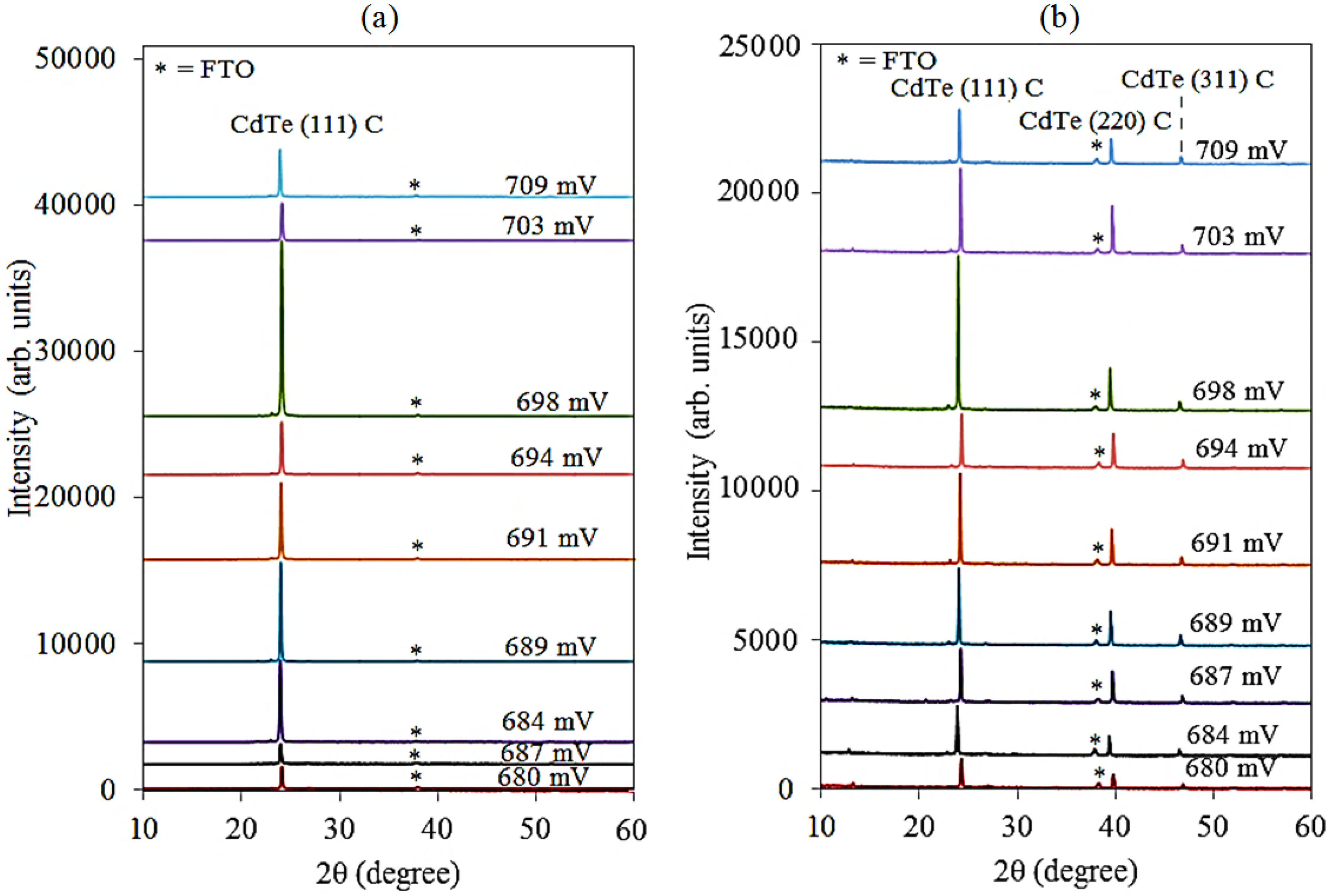
3.2.1. X-ray Diffraction

The X-ray diffraction studies were carried out on as-deposited and CdCl2 heat-treated CdTe layers and typical results are shown in 
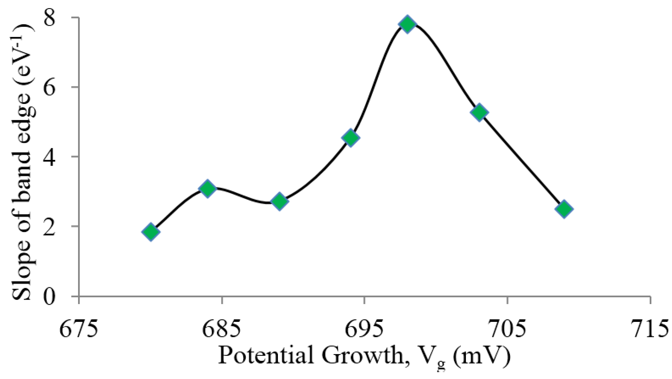
Figure 2a,b respectively. In this study, CdTe thin films were electrodeposited at different cathodic voltages from 680 to 709 mV. The CdCl2 heat treatment was performed at 400 °C for 20 min in air. According to Figure 2, both graphs show the presence of the noticeable peak of CdTe at 2θ = 24.15° corresponding to the (111) cubic phase. The highest crystallinity was observed at cathodic potential of 698 mV for both as-deposited and CdCl2 treated CdTe layers. In Figure 2b, most of the CdCl2 treated samples show a reduction of (111) CdTe peak as a general trend. Also the other peaks of cubic CdTe at 2θ = 39.46° and 46.58° were observed, corresponding to diffraction of (220) and (311) planes, respectively after CdCl2 treatment. This suggests that the reduction in (111) XRD peak is due to the loss of preferred orientation and grains becoming randomly orientated after CdCl2 heat treatment.
Figure 2. XRD patterns of CdTe thin films grown at cathodic voltage range of 680 to 709 mV for (a) as-deposited; and (b) CdCl2 treated samples at 400 °C for 20 min, in air.
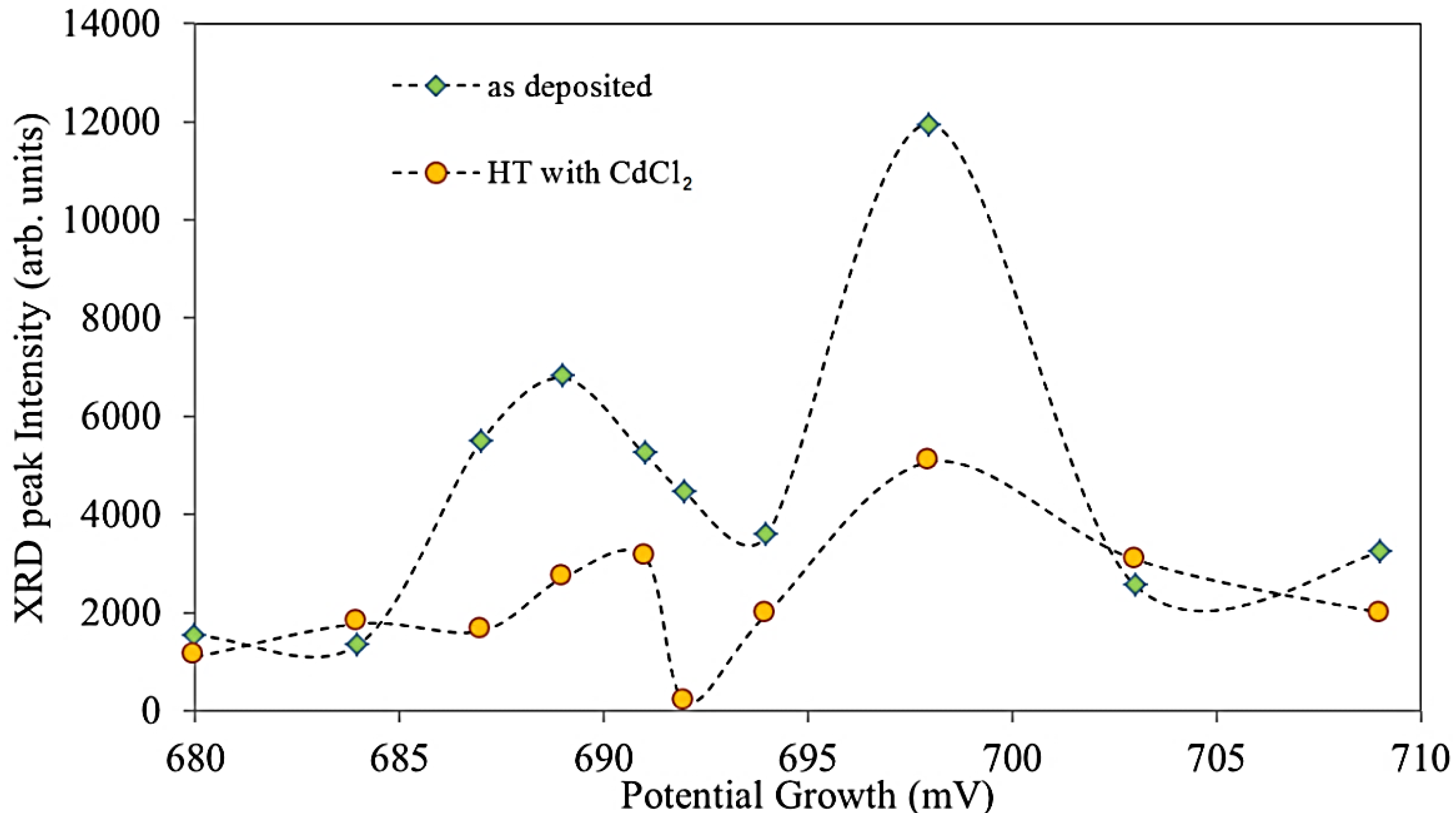
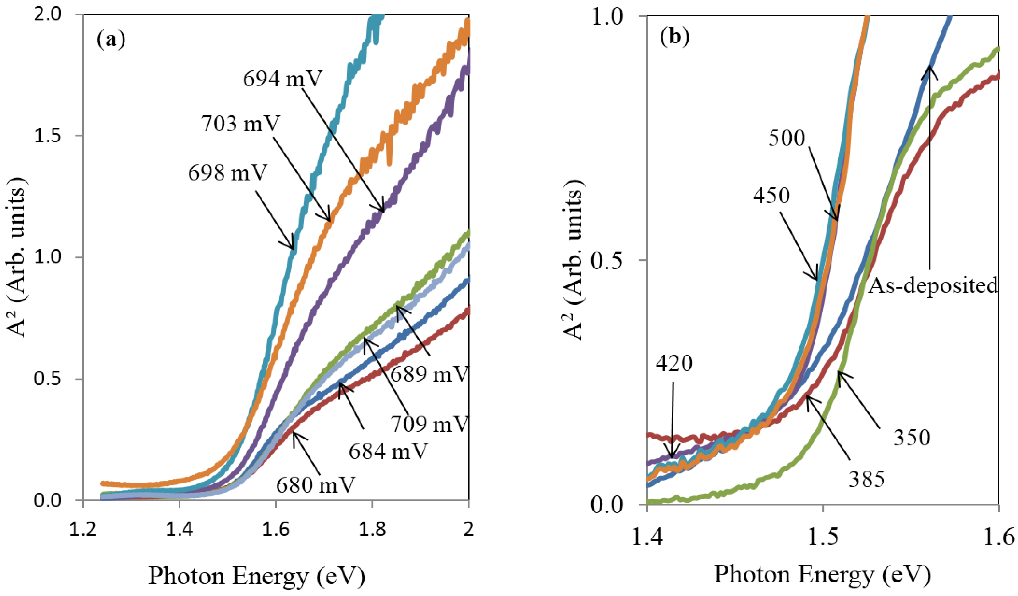
Energies 08 10883 g002
From Figure 3, it is observed that the most intense XRD peak is at Vg = 698 mV for both as-deposited and CdCl2 treated material. The high intensity of (111) peak indicates high crystallinity related to a stoichiometric material. The deviation from stoichiometric point reduced the crystallinity due to the Cd-rich or Te-rich CdTe. In a recent publication [19], a sudden phase transition was identified when CdTe layer is heat treated at 385 ± 5 °C in air, in the presence of CdCl2. At this temperature, the grain boundaries melt, and CdTe solid grains begin to float in a thin layer of melted liquid. Therefore, the grains suddenly lose their preferred orientation of (111) and show random orientations. Due to this sudden change, (111) peak collapses and the other two peaks (220) and (311) appear in the XRD spectra. In our heat treatment at 400 °C, this transition has just occurred and therefore intensity decreased in (111) peak and appearance of the other two peaks have been observed.
Figure 3. The intensity of (111) peak for as-deposited and CdCl2 treated CdTe layers.
Energies 08 10883 g003
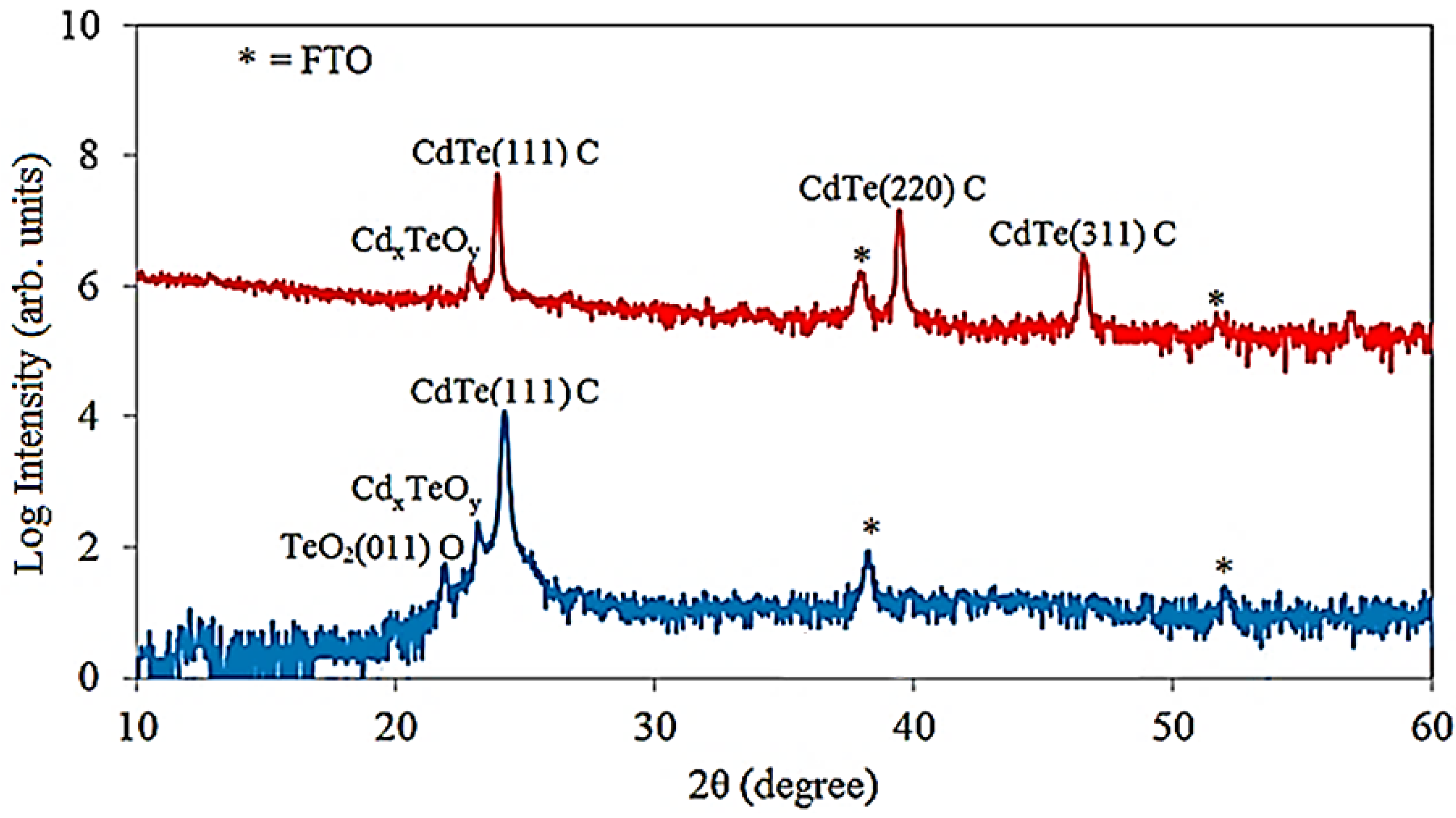
Figure 4 shows the XRD spectra plotted in log-scale in order to identify all peaks. These spectra are for as-deposited and CdCl2 treated CdTe layers grown at Vg = 698 mV. The as-deposited sample shows the appearance of small crystalline peaks of TeO2 and CdxTeOy at 2θ = 21.94° and 23.11° corresponding to the (011) orthorhombic and (111) monoclinic planes, respectively. These compounds incorporating oxygen are expected on the surface or in the material, since the layers are grown in atmospheric condition in aqueous solution. Also the prominent peak of (111) cubic CdTe is observed in as-deposited sample. The TeO2 peak disappeared while both (111) CdxTeOy and (111) CdTe peaks slightly reduced after CdCl2 treatment at 400 °C for 20 min. Also, after CdCl2 heat treatment, extra peaks were observed at 2θ = 39.46° and 46.58° which represent the cubic CdTe with (220) and (311) reflections respectively. It is well known that CdCl2 treatment usually improves the crystallinity of CdTe up to certain temperature [19,26,27]. However, after this temperature, a rapid reduction of (111) CdTe peak and the appearance of (220) and (311) peaks have been observed [12,28,29]. In a recent publication, this transition temperature has been identified as 385 ± 5 °C [19]. The XRD peak intensities, angles and occurrence of new peaks can be attributed to the random orientation of the grains in CdTe layers after melting of grain boundaries at ~385 °C. The summary of XRD data and obtained structural parameters of CdTe thin films grown at Vg = 698 mV are shown in Table 1. The crystallite size, D was calculated using the Scherrer’s formula:
D = 0.94  λ β cos θ
where λ is the wavelength of the X-rays used (1.541 Å), βis the full width at half maximum (FWHM) of the diffraction peak in radian and θ is the Bragg angle.
Figure 4. XRD patterns of as-deposited and CdCl2 treated CdTe layers grown at cathodic potential of 698 mV plotted in log-scale.
Energies 08 10883 g004
Table 1. Summary of XRD data for as-deposited and CdCl2 treated CdTe layers grown at cathodic potential of 698 mV.
SampleAngle 2θ°Lattice spacing D (Å)Intensity (a.u.)FWHM (Degrees)Crystallite size D (nm)Plane of orientation (hkl)Assignments
As-deposited CdTe21.944.00560.17348.9(0 1 1)TeO2/Orthorhombic
23.113.882390.13463.2-CdxTeOy
24.053.7112,3250.13463.3(1 1 1)CdTe/Cubic
CdCl2 HT CdTe23.043.911290.13463.2-CdxTeOy
24.153.7041020.13463.3(1 1 1)CdTe/Cubic
39.462.2813670.16752.8(2 2 0)CdTe/Cubic
46.581.932380.23338.8(3 1 1)CdTe/Cubic
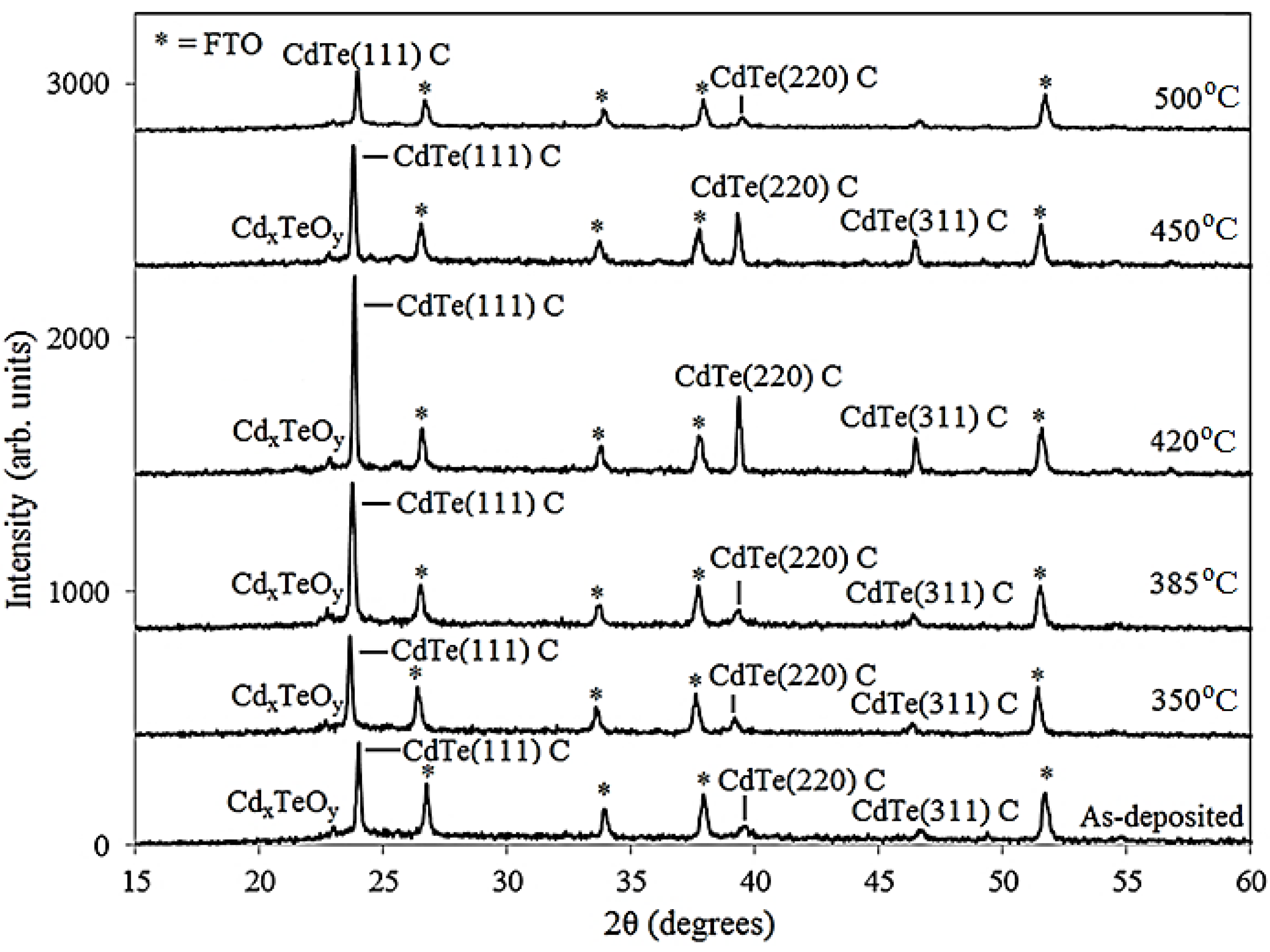
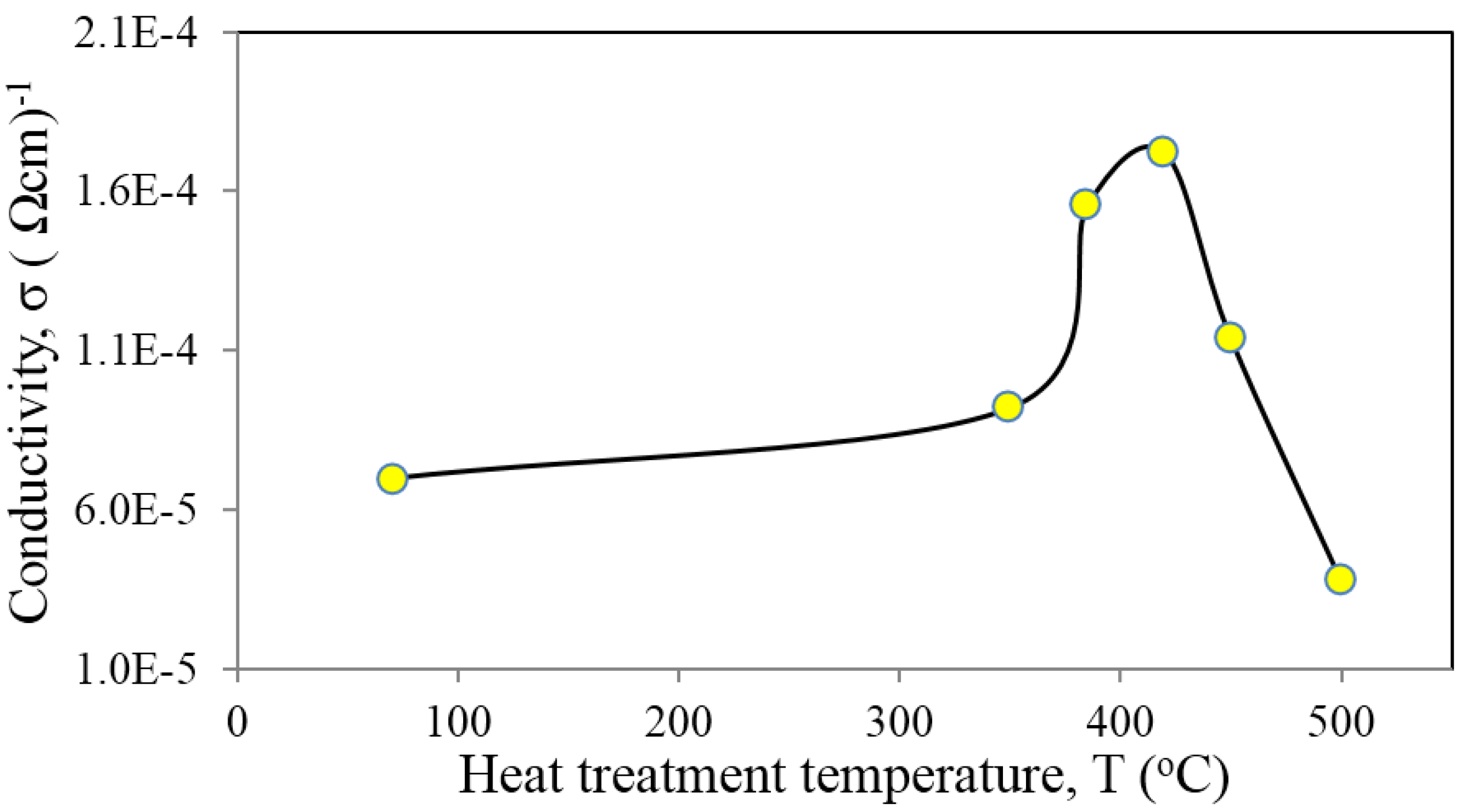
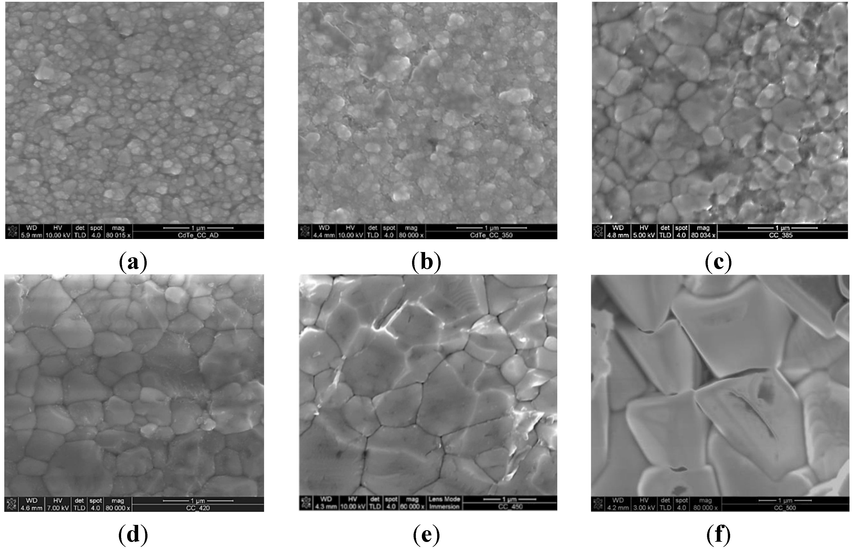
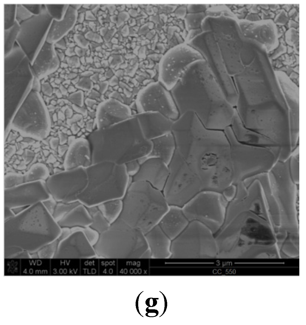
XRD spectra of CdTe layers after CdCl2 treatment at different temperatures up to 500 °C are shown in Figure 5. It seems that natural growth trend of CdTe on FTO is along (111) preferred orientation. The results in Figure 5 and Table 2 show that the intensity of (111) peak increases up to ~385 °C at the beginning. 385 ± 5 °C has been identified as the sudden transition temperature in the previous publication [19]. At this transition, the grain boundaries melt and the CdTe grains become randomly orientated. After melting of grain boundaries, the grains start to coalesce and form larger grains. The limitation of the Scherrer equation and XRD instrumentation prevent the determination of the size of these large grains, but SEM in 
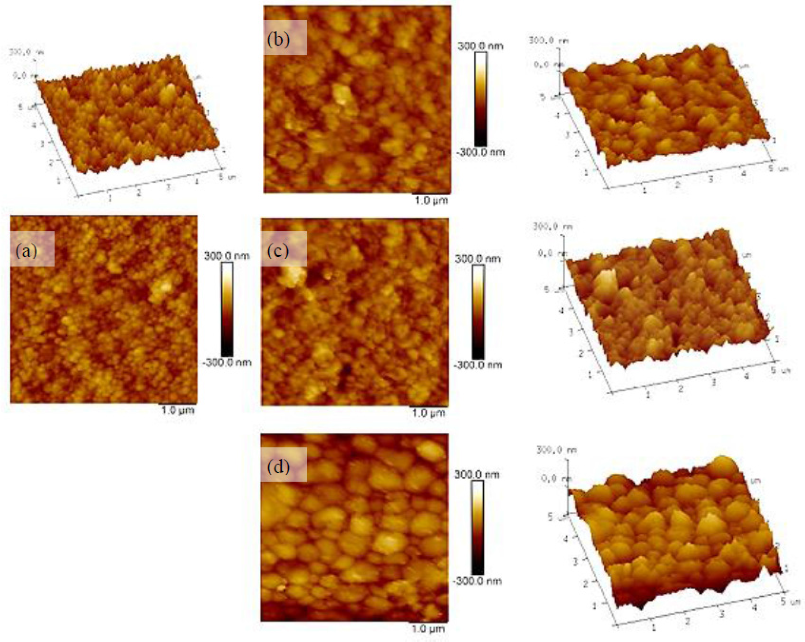
Figure 11, later clearly shows the formation of larger grains in the µm size. CdTe film treated at 420 °C demonstrated appearance of the other two peaks (220) and (311). However, heat treatment at 500 °C leads to reduction of all three peaks due to the loss of material via evaporation and sublimation. Therefore, the optimum temperature for heat treating lies in between 420 °C and 450 °C for electrodeposited CdTe layers from CdCl2 precursor.
Figure 5. Typical spectra for as-deposited CdTe and after CdCl2 treatment at 350, 385, 420, 450 and 500 °C for 20 min in air.
Energies 08 10883 g005
Table 2. Analysis of XRD peaks of CdTe for as-deposited and heat-treated with CdCl2 at different temperatures from 350 to 500 °C for 20 min in air.
Annealing temperature, T (°C)Peak intensity% Peak relative to 111 PeakCrystallite size calculated from (111) Peak, D (nm)
(111)(220)(311)(111)(220)(311)
As-deposited3731591004263.3
35038326121007363.3
38550138101008263.3
420730241109100331565.8
45043317666100411563.3
500235321110014563.3

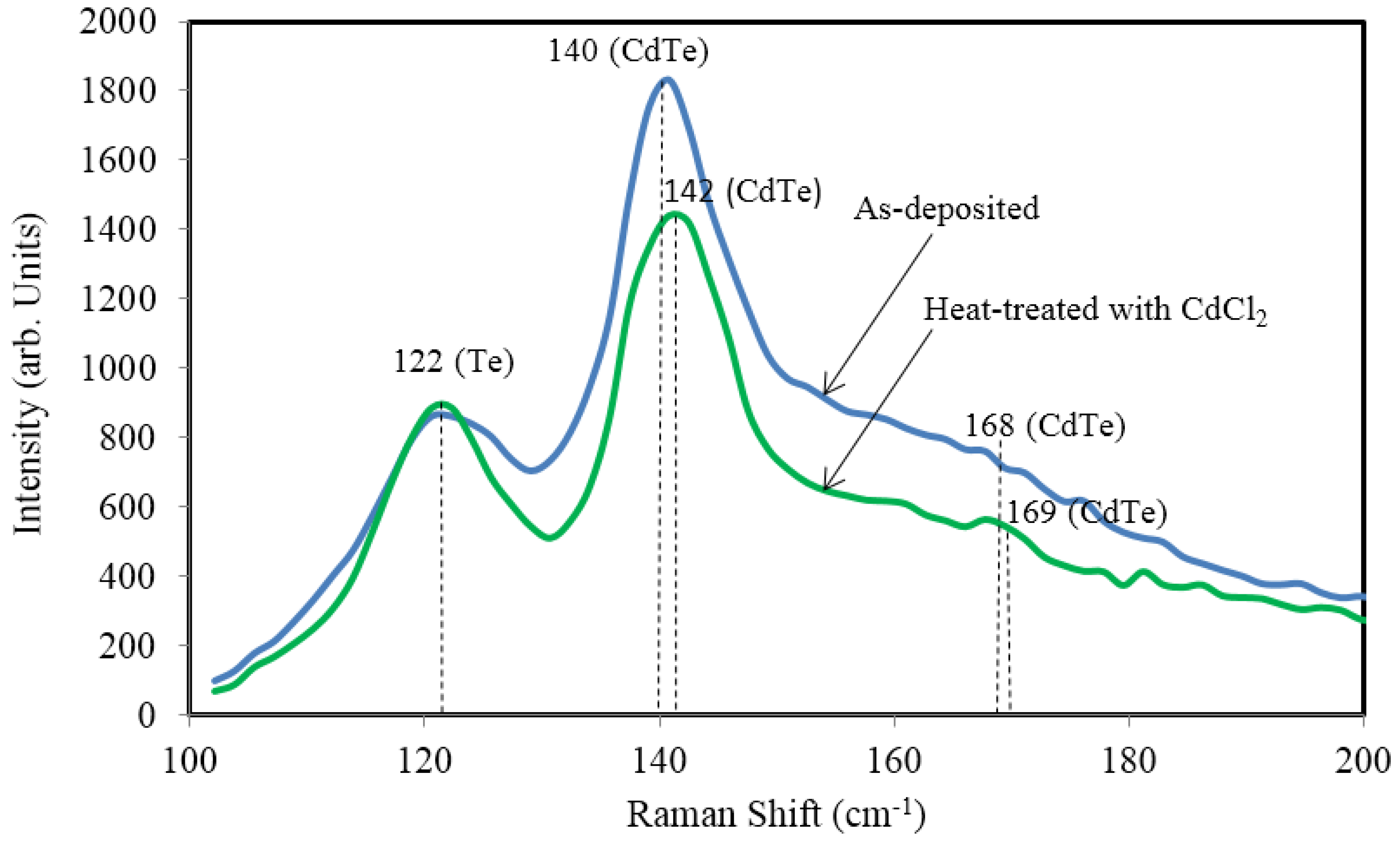
3.2.2. Raman Spectroscopy

Raman spectroscopy is an alternative and convenient method to identify material phases and determine the degree of crystallinity of the thin films. In this technique, vibration, rotation and other low-frequency modes in molecules are observed based on inelastic scattering of monochromatic radiation. The excitation source used in this work was 514 nm argon ion laser. The Raman spectra for as-deposited and CdCl2 treated CdTe layers are shown in Figure 6. The prominent peak of the as-deposited CdTe spectrum is observed at the wave number 140 cm−1 which represented the CdTe fingerprint. The Raman shift increased from 140 cm−1 to 142 cm−1 after CdCl2 treatment. This blue shift is due to the energy gained by the photon by increasing in the vibration mode and the lattice strain. The FWHM of this peak also increase slightly after CdCl2 treatment. There are two possible effects influencing the FWHM of the Raman peak which are size effect and the lattice dislocation effect [30]. In this case, the size effect is more pronounce since we observed the enlargement in crystallite size after CdCl2 heat-treatment. This trend is similar to the previous XRD results. It is also observed from this figure a Te peak at wave number of 122 cm−1 and the peak increased intensely after the CdCl2 heat-treatment. The spectrum for CdCl2 treated CdTe also shows one appearance of a small hump representing a CdTe peak at 168 cm−1. This particular sample shows improved crystallisation of excess Te in the CdTe layer after CdCl2 treatment. The summary of the Raman analysis is presented in Table 3.
Figure 6. Typical Raman spectra of CdTe thin films for as-deposited and CdCl2 treated at 400 °C for 20 min.
Energies 08 10883 g006
Table 3. Summary of Raman peak details for as-deposited and CdCl2 treated CdTe layers grown at 698 mV.
SamplesAs-depositedHT with CdCl2
Raman peak positions (cm−1)122 (Te)140 (CdTe)122 (Te)142 (CdTe)168 (CdTe)
Intensity (a.u.)86018318661421545
FWHM (cm−1)6.738.658.4110.201.78

3.3. Thickness Measurement

The thicknesses of electrodeposited CdTe layers at Vg = 698 mV, for different deposition periods were calculated theoretically by using Faraday’s laws of electroplating and experimentally using an optical profilometer. As shown in Figure 7a, the thickness obtained from the theoretical and experimental methods are similar. This shows that the loss of electronic charges for electrolysis of water is minimal under these growth conditions. It is observed that the deposition rate of CdTe thin film calculated from both theoretical and experimental values are 6 nm per minute. The thickness of CdTe thin films as a function of heat treatment temperatures from 350 to 500 °C were measured using optical profilometry and shown in Figure 7b From these measurements, it is observed that the thickness of the films decreased from 800 nm (as-deposited) to ~500 nm when the samples were heat treated at temperature up to 450 °C. The thickness shows rapid decline to 200 nm at temperature 500 °C which is due to the rapid loss of material through sublimation. Therefore the heat treatment of CdTe thin films in the presence of CdCl2 should be limited to temperature range of 420–450 °C to avoid the loss of material, and get all benefits of heat treatment.
Figure 7. Thickness of CdTe thin films as a function of (a) different deposition time at Vg = 698 mV; and (b) different heat treatment temperatures in the presence of CdCl2.
Energies 08 10883 g007

3.4. Electrical Characteristics Measurement

3.4.1. Photoelectrochemical (PEC) Cell

The PEC cell measurements were carried out in order to test the electrical conductivity type of CdTe layers. Glass/FTO/CdTe were immersed in 0.1 M Na2S2O3 aqueous solution to form a solid/liquid junction at CdTe/electrolyte interface. The voltage produced at the junction was measured with respect to a carbon counter electrode under dark and illuminated conditions. The difference in voltages provides the open circuit voltage of the solid/liquid junction, or the PEC signal. The system was first calibrated with a known material like n-CdS, and the sign of the PEC signal shows the electrical conductivity type of the CdTe layers. Figure 8a shows the trend of PEC signal for as-deposited and CdCl2 treated CdTe thin films as a function of growth voltage, Vg. It is observed that the as-deposited CdTe samples grown at lower voltages (Vg < 700 mV) are n-type and those which are grown at higher voltages (Vg ≥ 700 mV) are p-type.
These results show complete contrast to the CdTe grown by CdSO4 [19] and Cd(NO3)2 [12] recursors in Figure 8b,c, respectively. Figure 8b,c show typical PEC results obtained from CdTe layers grown using sulphate and nitrate pre-cursors without the presence of Cl in the bath. These results behave according to electrodeposition principles. According to E° values of Te (+0.593 V) and Cd (−0.403 V) with respect to hydrogen electrode, CdTe electrodeposited below the stoichiometric point (Vi) show p-type electrical conductivity due to Te-richness, while CdTe layers grown above Vi show n-type electrical conductivity due to Cd-richness. This variation is mainly due to the change of composition in the absence of external doping agent. This has been reported earlier from our previous work using sulphate and nitrate precursors [11,12,19]. Completely opposite results observed for CdTe layers grown from chloride precursor are therefore due to the “built-in CdCl2 treatment” during the growth. This needs careful further experimentation and critical analysis, and future work is focused on this subject.
Figure 8. PEC signals as a function of growth voltage, for (a) as-deposited and CdCl2 treated CdTe layer grown from chloride precursor and as-deposited CdTe layers grown using; (b) sulphate [19]; and (c) nitrate precursor [12].
Energies 08 10883 g008
After heat-treatment at 400 °C for 20 min, in the presence of CdCl2, all samples become p-type in electrical conductivity. This provides a clue for CdTe becoming p-type in electrical conductivity when high concentration of Cl is present in the material. Therefore doping effects seem to be drastic depending on the initial composition of CdTe layer and the concentration of Cl present for doping the material. In this case, the electrical conductivity depends on these doping effects, namely the composition variation and the inclusion of Cl during growth in CdCl2 solution. The detailed investigation is currently progressing to improve our understanding on CdCl2 treatment.
PEC cell measurements for samples heat-treated with CdCl2 at different temperatures are shown in Table 4. The as-deposited CdTe thin film electrodeposited closed to 698 mV is n-type. However, the electrical conductivity type of these samples have changed to p-type after CdCl2 treatment at 350, 385 and 420 °C. This can happen due to the changing of doping profile or material deterioration. Doping profile could change due to incorporation of elements such as Cl, in CdTe crystal. During deposition, Cl can be within grain boundaries, but heat treatment electrically activated these by adding to the CdTe crystal lattice. Doping profile can also change due to loss of one element during heat treatment. As shown in Figure 9, Cd has higher vapour pressure than Te [31]. Therefore Cd tends to evaporate easily during annealing since material with higher vapour pressure tends to evaporate earlier than those with lower vapour pressure. Krishnamurthy et al. have also reported that the Cd sublimation energy to terminate the surface of CdTe layer is much smaller than Te [32]. Therefore, Cd atom should be much easier to remove than Te leaving Te-rich p-type CdTe layer. Therefore, the as-deposited CdTe with n-type electrical conductivity changed to p-type after annealing at 350 to 420 °C. However, those samples annealed at 450 °C and above have demonstrated n-type electrical conductivities. We believe that the high annealing temperature (T ≥ 450 °C) has initiated deterioration of the layer through sublimation. Also CdTe annealed at 550 °C did not show any PEC signal since the layer has completely deteriorated (see Figure 10). These results agree with XRD data presented in Table 2.
Table 4. The PEC signal of CdTe grown near cathodic potential of 698 mV with variation of annealing temperature from 350 °C to 550 °C.
SamplePEC signalElectrical conductivity typeComments
As-deposited−70ngrown at Vg = 698 mV
35062pconductivity change due to doping effects
38578p
42055p
450−64nmaterial degradation is taking place
500−9n
550no signalthe layer did not survive
Figure 9. The vapour pressure of cadmium and tellurium as a function of temperature.
Energies 08 10883 g009
Figure 10. The electrical conductivity of CdTe after CdCl2 treatment at different annealing temperatures.
Energies 08 10883 g010

3.4.2. DC Conductivity Measurements

DC conductivity measurements were carried out in order to determine the electrical conductivity of as-deposited and CdCl2 heat-treated CdTe layers. For these experiments, thicker layers were used in order to avoid leakage through pinholes. 2 mm diameter and circular ohmic contacts were made by evaporating Al layer for n-type samples and Au layer for p-type samples through a metallic mask. The resistance of CdTe layers were measured using I-V characteristics and the average resistance of each sample was measured and the conductivity was calculated with known thicknesses and area of FTO/CdTe/Al or Au structures.
Table 5 summarizes the measurements of average resistances, resistivity and electrical conductivity of CdTe layers deposited near Vg = 698 mV (n-type) and heat treated with CdCl2 at different temperatures. Figure 10 shows that the value of electrical conductivity has increased from 6.97 × 10⁵ to 17.19 × 10⁵ (Ω·cm)−1 after heat treatment with CdCl2 at temperature of 420 °C. The conductivity enhancement is due to the improvement of crystallinity, enlargement of the grain size and re-distribution of dopants [33] which promote higher mobility of electrons. However, a decrease in conductivity was observed for the CdCl2 treated samples at annealing temperatures ≥450 °C. This must be due to the deterioration of the material at higher annealing temperatures and this trend also is consistence with the material deterioration observed in both XRD and PEC analyses in previous sections.
Table 5. The summary of electrical properties of CdTe thin films grown near Vg = 698 mV, and heat treated at different temperatures in the presence of CdCl2.
SamplesAverage resistance (Ω)Resistivity, ρ × 104 (Ω·cm)Conductivity, σ × 10−5 (Ω·cm)−1
As deposited31.11.436.97
CC-35026.01.099.19
CC-38512.30.6415.53
CC-42011.10.5817.19
CC-45014.00.8811.42
CC-50017.62.673.75

3.5. Microstructure and Morphological Studies

3.5.1. Scanning Electron Microscopy

Figure 11 shows the SEM images of CdTe thin films for as-deposited and annealed at 350, 385, 420, 450, 500 and 550 °C in the presence of CdCl2. The as-deposited CdTe shows the grains size in a range of 150 to 200 nm. As the annealing temperatures were increased, the grains start to coalesce together forming larger grains. The CdCl2 treated CdTe at 420 and 450 °C show grain sizes in (700–900) nm and (1000–4000) nm ranges, respectively. The presence of CdCl2 during the heat treatment has enhanced the coalescence of smaller nano-crystallites into larger crystals to improve material layers. Many researchers observed the grain growth appearance together with gaps in between grains after CdCl2 treatment. The existence of gaps in the CdTe layers will cause a catastrophic impact on the performance of solar cells due to short circuiting devices. However, CdTe layers grown in this work show a compact grain growth without any gaps appearing after CdCl2 heat-treatment around 420 °C. This suggests that CdCl2 treated CdTe produced from chloride precursor has a better quality for solar cell devices since it has no obvious gaps and the larger grain sizes for less scattering at grain boundaries and with high electron mobility. Heat treatment at 500 °C and above seems to open up gaps between grains and therefore deteriorates the layers. Also, Figure 11g shows the SEM image for CdTe annealed at 550 °C. It exposes the appearance of FTO surface image since CdTe layer did not survive at high temperature due to the loss of material. These observations confirm the results observed from XRD, PEC and DC measurements in this work. The optimum heat treatment seems to be between 420 and 450 °C and this could be finalised during device fabrication. It is also an important point to note that the ED-CdTe layers grown at low temperature (~65°) attain comparable grain sizes (~few micron size) to CSS-CdTe after CdCl2 treatment.
Figure 11. SEM images of CdTe grown at 698 mV for (a) as-deposited; and annealed at (b) 350; (c) 385; (d) 420; (e) 450; (f) 500; and (g) 550 °C for 20 min.
Energies 08 10883 g011aEnergies 08 10883 g011b

3.5.2. Atomic Force Microscopy

AFM is a convenient technique to study the morphology and surface roughness of thin films. Figure 12 shows the typical 1.5 μm × 1.5 μm AFM micrographs of (a) as-deposited; and after CdCl2 treatment at temperatures (b) 385; (c) 420; and (d) 450 °C. The brightness of these micrographs indicate the variation of depth of the surface morphology. It is observed that the as-deposited CdTe shows a surface with homogeneous brightness which suggest that the layer is uniform due to the formation of smaller grains. The CdCl2 treated samples show variation of brightness which represents the formation of valleys and peaks on the surface. The roughness of the films increased as the annealing temperature increased due to the enlargement of the grain size especially forming columnar type grains, growing upwards. The average surface roughness for the as-deposited CdTe and CdCl2 treated CdTe are shown in Table 6.
Figure 12. Typical AFM images of (a) as-deposited; and heat treated with CdCl2 at (b) 385 °C; (c) 420 °C; and (d) 450 °C. These layers have been annealed for 20 min in atmospheric condition.
Energies 08 10883 g012
Table 6. The AFM data on surface roughness of CdTe thin films, as a function of annealing temperatures.
SampleRms (nm)
As-deposited25.7
CdCl2 heat-treated at 385 °C38.0
CdCl2 heat-treated at 420 °C54.3
CdCl2 heat-treated at 450 °C68.7

3.6. Optical Properties

The optical absorption measurements of the CdTe layers were carried out using a UV-Vis spectrophotometer in the wavelength range 600–1000 nm. The square of absorbance (A2) has been plotted as a function of photon energy, and the bandgap energy was estimated by extrapolating the straight-line segment of the graph to the photon energy axis. Figure 13a shows optical absorption of the as-deposited CdTe thin films grown at different cathodic voltages from 680 to 709 mV. It is observed that the bandgap energy of as-deposited CdTe films was in the range of 1.48 to 1.51 eV. The average error of these measurements is ±0.02 eV. The graphs in Figure 13a and Figure 14 show that the trend of applied absorption edge is increased with Vg up to 698 mV and then gradually reduces with further increment of Vg. The reduction of bandgap with higher Vg is due to deposition of metallic Cd with zero bandgap. Figure 13b shows the optical absorption spectra of CdTe thin films heat treated at temperatures from 350 to 500 °C in the presence of CdCl2.
Figure 13. Optical absorption of CdTe thin films for (a) as-deposited with different Vg; and (b) as-deposited and CdCl2 treated at different temperatures.
Energies 08 10883 g013
Figure 14. Slope of band edge versus Vg for as deposited CdTe thin films. Highest absorption edge indicates the optimum growth voltage.
Energies 08 10883 g014
The bandgap of CdTe layers have decreased with higher annealing temperature. The decrease in the bandgap after annealing temperature >385 °C can be due to the recrystallization, increase in grain size and stress [34]. This can also be due to the removal of pin-holes in the layer thereby preventing the photons through the pin-holes. The summary of the optical band energy with different Vg and annealing temperature of CdCl2 treatment is shown in Table 7.
Table 7. The optical bandgap of CdTe layers grown at different Vg and bandgap as a function of CdCl2 heat treatment temperature for CdTe grown at Vg = 698 mV.
Cathodic voltage, Vg (mV)Band energy, Eg (eV)CdCl2 treated temperatures, T (°C)Band energy, Eg (eV)
6801.48651.49
6841.493501.49
6891.513851.49
6941.514201.46
6981.494501.45
7031.485001.46
7091.49

4. Conclusions

CdTe thin films have successfully been grown by electrodeposition using cadmium chloride precursor. XRD results show presence of the prominent peak of (111) cubic CdTe in as-deposited and appearance of another two peaks of (220) and (311) cubic CdTe after CdCl2 treatment above 385 °C. This confirms the phase change taking place above ~385 °C as previously identified and reported. PEC cell measurement shows a possibility to grow p-, i- and n-type CdTe layers by tuning the Vg during electrodeposition. Noticeable changes in CdTe grain size were observed after CdCl2 treatment and these grains up to 4 µm are comparable to high temperature grown CdTe layers with large grains. The optical bandgap of stoichiometric CdTe grown at 698 mV is 1.47 eV. The work is progressing to understand the unique properties observed in electrical conduction type, morphology and to use these layers in solar cell device structures.

Acknowledgments

The authors would like to thank A. Ojo, B.Y. Kadem, P.A. Bingham, F. Fauzi and O.K. Echendu for their valuable contributions. The main author would also like to acknowledge the Ministry of Higher Education, Malaysia and National Defence University of Malaysia for financial support. The authors declare there is no conflict interest.

Author Contributions

The preparation and electrodeposition of CdTe thin films were done by Nor Azlian Abdul-Manaf. She was also responsible for the thin film characterisations. In addition, this work was also performed under the advisement of and regular feedback from Prof I. M. Dharmadasa, who also revised the manuscript critically. Moreover, Hussein I. Salim, Mohammad L. Madugu and Olajide I. Olusolaalso gave some useful suggestions for this work and helped revise the manuscript.

Conflicts of Interest

The authors declare no conflict of interest.

References

  1. First Solar Raises Bar for CdTe with 21.5% Efficiency Record. Available online: http://www.pv-magazine.com/news/details/beitrag/first-solar-raises-bar-for-cdte-with-215-efficiency-record_100018069/#ixzz3faM4fEOOI (accessed on 20 February 2015).
  2. Takamoto, T.; Agui, T.; Kurita, H.; Ohmori, M. Improved junction formation procedure for low temperature deposited CdS/CdTe solar cells. Sol. Energy Mater. Sol. Cells 1997, 49, 219–225. [Google Scholar] [CrossRef]
  3. Shao, M.; Fischer, A.; Grecu, D.; Jayamaha, U.; Bykov, E.; Contreras-Puente, G.; Bohn, R.G.; Compaan, A.D. Radio-frequency-magnetron-sputtered CdS/CdTe solar cells on soda-lime glass. Appl. Phys. Lett. 1996, 69, 3045–3047. [Google Scholar] [CrossRef]
  4. Boone, J.L.; van Doren, T.P.; Berry, A.K. Deposition of CdTe by spray pyrolysis. Thin Solid Films 1921, 87, 259–264. [Google Scholar] [CrossRef]
  5. Chu, T.L.; Chu, S.S.; Ferekides, C.; Wu, C.Q.; Britt, J.; Wang, C. 13.4% efficient thin-film CdS/CdTe solar cells. J. Appl. Phys. 1991, 70, 7608–7612. [Google Scholar] [CrossRef]
  6. Bonnet, D. Manufacturing of CSS CdTe solar cells. Thin Solid Films 2000, 361–362, 547–552. [Google Scholar] [CrossRef]
  7. Faust, C.L. Electrodeposition of alloys, 1930-1940. J. Electrochem. Soc. 1940, 78, 383–421. [Google Scholar] [CrossRef]
  8. Panicker, M.P.R.; Knaster, M.; Kröger, F.A. Cathodic deposition of CdTe from aqueous electrolytes. J. Electrochem. Soc. Electrochem. Sci. Technol. 1978, 125, 566–572. [Google Scholar] [CrossRef]
  9. Das, S.K.; Morris, G.C. Preparation and characterization of electrodeposited n-CdS/p-CdTe thin film solar cells. Sol. Energy Mater. Sol. Cells 1993, 28, 305–316. [Google Scholar] [CrossRef]
  10. Ou, S.S.; Basol, O.M.; Stafsudd, B.M. Optical properties of electrochemically deposited CdTe films. J. Appl. Phys. 1984, 55, 3769–3772. [Google Scholar] [CrossRef]
  11. Dharmadasa, I.M.; Haigh, J. Strengths and advantages of electrodeposition as a semiconductor growth technique for applications in macroelectronic devices. J. Electrochem. Soc. 2006, 163, G47–G52. [Google Scholar] [CrossRef]
  12. Salim, H.I.; Patel, V.; Abbas, A.; Walls, J.M.; Dharmadasa, I.M. Electrodeposition of CdTe thin films using nitrate precursor for applications in solar cells. J. Mater. Sci. Mater. Electron. 2015, 26, 3119–3128. [Google Scholar] [CrossRef]
  13. Dalchiele, E.A.; Bonilla, S. Electrodeposition of CdTe polycrystalline thin films: Influence of electroyte anions in film composition. J. Braz. Chem. Soc. 1992, 3, 95–97. [Google Scholar] [CrossRef]
  14. Lincot, D. State-of-the-Art Program on Compound Semiconductors: (SOTAPOCS XLII) and Processes at the Compound-Semiconductor/Solution Interface: Proceedings of the International Symposia; Chang, P.C., Ed.; The Electrochemical Society: Montreal, QC, Canada, 2005; pp. 107–119. [Google Scholar]
  15. Ham, D.; Mishra, K.K.; Weiss, A.; Rajeshwar, K. Anodic electrosynthesis of cadmium telluride (CdTe) thin films. Chem. Mater. 1989, 1, 619–625. [Google Scholar] [CrossRef]
  16. Pandey, R.K.; Maffib, S.; Bicelli, L.P. Study of the CdTe electrodeposition from a nonaqueous bath. J. Mater. Chem. Phys. 1993, 35, 15–20. [Google Scholar] [CrossRef]
  17. Chaure, N.B.; Samantilleke, A.P.; Dharmadasa, I.M. The effects of inclusion of iodine in CdTe thin films on material properties and solar cell performance. Sol. Energy Mater. Sol. Cells 2003, 77, 303–317. [Google Scholar] [CrossRef]
  18. Nakayama, N.; Matsumoto, H.; Yamaguchi, K.; Ikagami, S.; Hioki, Y. Ceramic thin film CdTe solar cell. Jpn. J. Appl. Phys. 1976, 15, 2281–2282. [Google Scholar] [CrossRef]
  19. Dharmadasa, I.M.; Bingham, P.A.; Echendu, O.K.; Salim, H.I.; Druffel, T.; Dharmadasa, R.; Sumanasekera, G.U.; Dharmasena, R.R.; Dergacheva, M.B.; Mit, K.A.; et al. Fabrication of CdS/CdTe-based thin film solar cells using an electrochemical technique. Coatings 2014, 4, 380–415. [Google Scholar] [CrossRef] [Green Version]
  20. Schulmeyera, T.; Fritsche, J.; Thißen, A.; Klein, A.; Jaegermann, W.; Campo, M.; Beier, J. Effect of in situ UHV CdCl2-activation on the electronic properties of CdTe thin film solar cells. Thin Solid Films 2003, 431–432, 84–89. [Google Scholar] [CrossRef]
  21. Rami, M.; Benamar, E.; Fahoume, M.; Chraibi, F.; Ennaoui, A.M.J. Effect of heat-treatment with CdCl2 on the electrodeposited CdTe/CdS heterojunction. Condens. Matter 2000, 3, 66–70. [Google Scholar]
  22. Dharmadasa, I.M. Review of the CdCl2 treatment used in CdS/CdTe thin film solar cell development and new evidence towards improved understanding. Coatings 2014, 4, 282–307. [Google Scholar] [CrossRef]
  23. Bonilla, S.; Dalchiele, E.A. Electrochemical deposition and characterization of CdTe polycrystalline thin films. Thin Solid Films 1991, 204, 397–403. [Google Scholar] [CrossRef]
  24. Pandey, R.K.; Sahu, S.N.; Chandra, S. Handbook of Semiconductor Electrodeposition, 1st ed.; Marcel Dekker, Inc.: New York, NY, USA, 1996. [Google Scholar]
  25. Vanysek, P. CRC Handbook of Chemistry and Physics, 91th ed.; Chemical Rubber Company (CRC) Press: Boca Raton, FL, USA, 2000. [Google Scholar]
  26. Bacaksiz, E.; Basol, B.M.; Altunbaş, M.; Novruzov, V.; Yanmaz, E.; Nezir, S. Effects of substrate temperature and post-deposition anneal on properties of evaporated cadmium telluride films. Thin Solid Films 2007, 515, 3079–3084. [Google Scholar] [CrossRef]
  27. Garadkar, K.M.; Pawar, S.J.; Hankare, P.P.; Patil, A.A. Effect of annealing on chemically deposited polycrystalline CdTe thin films. J. Alloy. Compd. 2010, 491, 77–80. [Google Scholar] [CrossRef]
  28. Paulson, P.D.; Dutta, V. Study of in situ CdCl2 treatment on CSS deposited CdTe films and CdS/CdTe solar cells. Thin Solid Films 2000, 370, 299–306. [Google Scholar] [CrossRef]
  29. Lee, J. Effects of heat treatment of vacuum evaporated CdCl2 layer on the properties of CdS/CdTe solar cells. Curr. Appl. Phys. 2011, 11, S103–S108. [Google Scholar] [CrossRef]
  30. Shen, M.Y.; Saito, M.; Goto, T.; Sato, F.; Tanaka, M. Structure and optical properties of CdTemicrocrystallites in CaF2. J. Phys. Condens. Matter 1994, 6, 8479–8486. [Google Scholar] [CrossRef]
  31. VaporPressures of the Elements (Data Page). Available online: http://en.wikipedia.org/wiki/Vapor_pressures_of_the_elements_%28data_page%29 (accessed on 26 May 2015).
  32. Krishnamurthy, S.; Berding, M.A.; Sher, A.; Chen, A.B. Semiconductor surface sublimation energies and atom-atom interactions. Chem. Phys. Rev. Lett. 1990, 64, 2531–2535. [Google Scholar] [CrossRef]
  33. Dharmadasa, I.M.; Echendu, O.K.; Fauzi, F.; Abdul-Manaf, N.A.; Salim, H.I.; Druffel, T.; Dharmadasa, R.; Lavery, B. Effects of CdCl2 treatment on deep levels in CdTe and their implications on thin film solar cells: A comprehensive photoluminescence study. J. Mater. Sci. Mater. Electron. 2015, 26, 4571–4583. [Google Scholar] [CrossRef]
  34. Enriquez, J.P.; Mathew, X. The effect of annealing on the structure of CdTe films electro-deposited on metallic substrates. J. Cryst. Growth 2003, 259, 215–222. [Google Scholar] [CrossRef]

