
Design of a Gate-Driving Cell for Enabling Extended SiC MOSFET Voltage Blocking


1
Electrical Engineering Department, Sheffield Hallam University, Sheffield S1 1WB, UK
2
School of Engineering, University of Warwick, Coventry CV4 7AL, UK
*
Author to whom correspondence should be addressed.
Energies 2022, 15(20), 7768; https://doi.org/10.3390/en15207768
Submission received: 20 September 2022
/
Revised: 15 October 2022
/
Accepted: 18 October 2022
/
Published: 20 October 2022
(This article belongs to the Section F3: Power Electronics)
Abstract
:A series connection of SiC MOSFETs for kV blocking capability can enable more design flexibility in modular multi-level converters as well as other topologies. In this paper, a novel gate driver circuit capable of driving series-connected SiC MOSFETs for high voltage applications is proposed. The primary advantage of the proposed design is that a single gate driver was used to switch all the series devices. The circuit used switching capacitors to sequentially charge and discharge device gate capacitances during switching and enable a negative turn-off voltage to avoid device coupling from Miller-capacitive feedback effects. With the proposed gate driver design and appropriate component values selection, avalanche breakdown due to voltage divergence during switching transients could be avoided with only a minor imbalance in the top device. Simulations and experimental measurements showed that the zero-current turn-off transition of all switches was achieved, and this approved the validity of the design.
1. Introduction
In the recent years, wide-bandgap semiconductor devices have enabled more improvements in applications in the power electronics field [1]. At the time when silicon (Si) devices are coming close to the limitations of the material, the high switching speed offered by silicon carbide (SiC) materials, alongside their high breakdown voltage and high thermal conductivity make them superior to Silicon (Si). SiC MOSFET is a promising alternative in medium- and high-voltage power electronics applications [2].
Existing commercial SiC MOSFETs are still commonly 1.2 and 1.7 kV. Some higher voltage SiC switches are in the development stage and, if available commercially, they would be costly [3,4]. According to the work in [5], series-connected SiC MOSFETs brings a lower on-resistance which allows for higher current density than using a single high-voltage device. Therefore, investigating the series connection of multiple SiC MOSFETs does worth.
For series connection of MOSFET switches, the common driving method uses fully separated drivers for each device equipped with its own isolated power supply [6]. Although this method provides more control flexibility, it brings some challenges in terms of compact designs for high power density applications [7]. An auxiliary voltage source was required in [8] to provide enough power to drive the upper devices.
One way to drive the upper-side MOSFETs without an auxiliary power supply [8] is by using capacitive coupling [9], where the lowest MOSFET acts as a master and the upper ones as slaves. The concept uses the charge variation in the capacitor to produce the driving signals for the upper MOSFETs. A floating self-driving circuit was developed in [10,11] utilizing DC capacitors to support switching the high side of two series switches. Another concern while driving series MOSFET devices is the off- state voltage balancing during both the steady state and dynamic transition [12]. Uneven leakage current between series MOSFETs is the main reason behind the unbalanced voltage distribution. Equal parallel resistors across series MOSFETs will not always guarantee a balanced voltage if the leakage current is significant. An active control technique was proposed in [13] to achieve dynamic sharing for series IGBTs. Ruchira et al. in [14] proposed a voltage-clamping circuit to balance the voltages. In [15], a snubber circuit was presented to achieve adequate voltage sharing during the transient across series-connected SiC MOSFETs. To mitigate the false turn-on events and provide more gate immunity, a negative voltage, i.e., −5 V is recommended to switch-off the MOSFET [7].
Active gate driving for IGBTs was proposed in [16] for both switching loss reduction and voltage balancing of the series-connected IGBTs. A quasi-active gate control uses a simple RC network to balance the voltage in [17]. A single-gate driver for series SiC MOSFETs was designed for solid-state circuit breaker (SSCB) applications in [7,18] and the design is simple and compact. Particularly for SiC MOSFETs, other designs of single-gate drivers are reviewed in [19,20], where some of them depended on adding a more peripheral circuit to shape the driving signal or to determine the slope to mitigate electromagnetic interference (EMI) issues. A gate driver dedicated to SiC MOSFET modules is presented in [21]. Usually, voltage gate driving is used for gate driving, however, in [22] a current-source gate driver for SiC MOSFETs was developed, which contributed to less switching losses, but the development was just for an individual switch. It is a competitive solution for SiC MOSFETs where its gate capacitance is much less than for Si MOSFETs, for example.
In all previous studies, the component selection for voltage balance circuits has depended on the test conditions and no generalized design has been developed. In addition, most of the designs are not modular for duplication and use a different numbers of series MOSFETs.
The contribution of this paper is in presenting a new modular design of a single-gate driving cell able to drive a stack of series MOSFETs with a systematic design rule. The cell design was able to bias the MOSFETs gates at a negative voltage level. The design criteria of all the components are stated with LTspice simulation validation. The driven MOSFETs were able to switch voltages in the KV range with a switching transition less than 100 ns, in addition to balancing the voltage among all MOSFETs at the off-state. Zero-current switching (ZCS) was achieved during turn-off transition. The focus here was on SiC but the design can be used for other MOSFETs technologies with some value amendments. The experimental results of the designed prototype achieved coherent switching under double-pulse testing with a clamped inductive load.
2. The Proposed Driving Cell
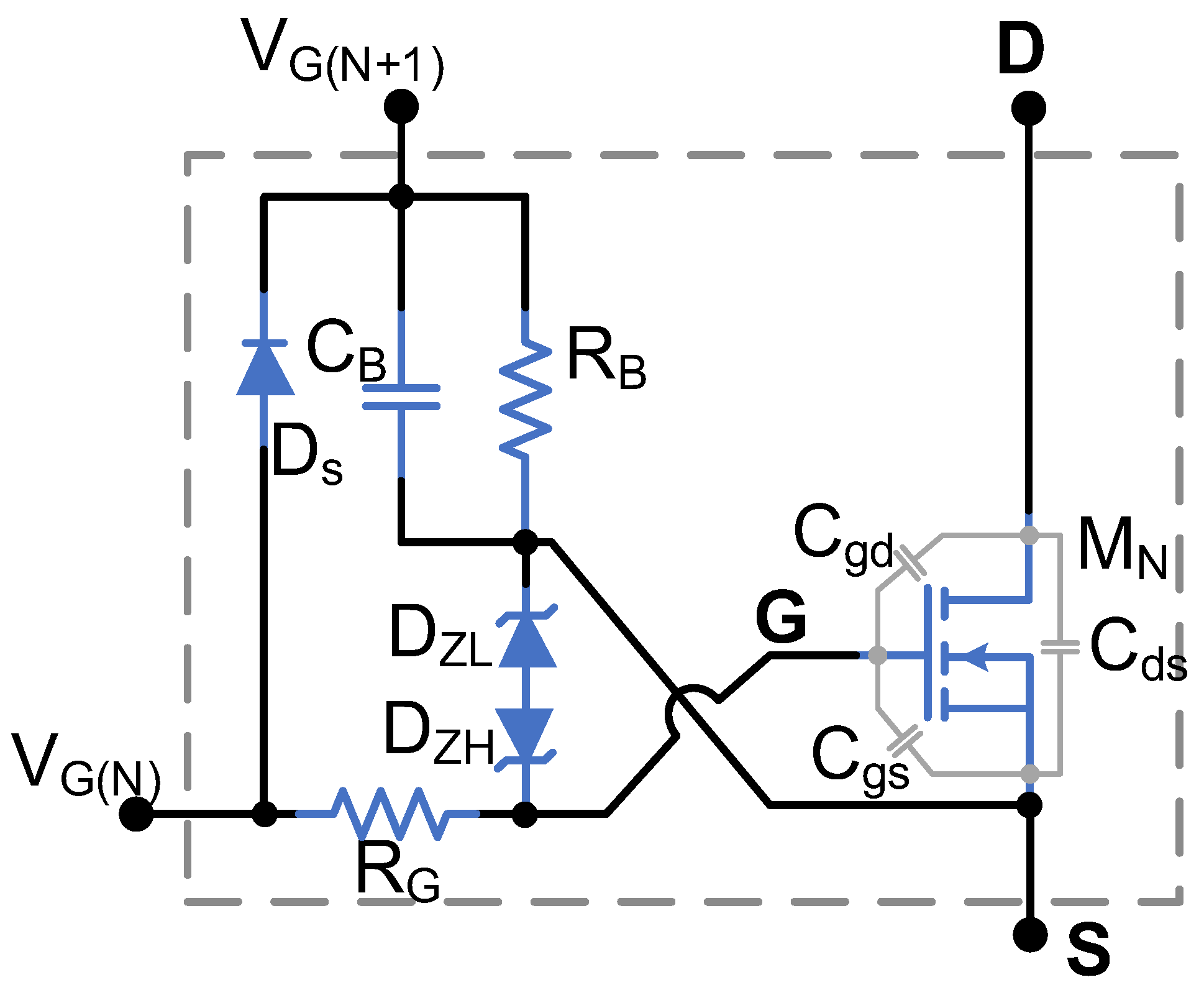
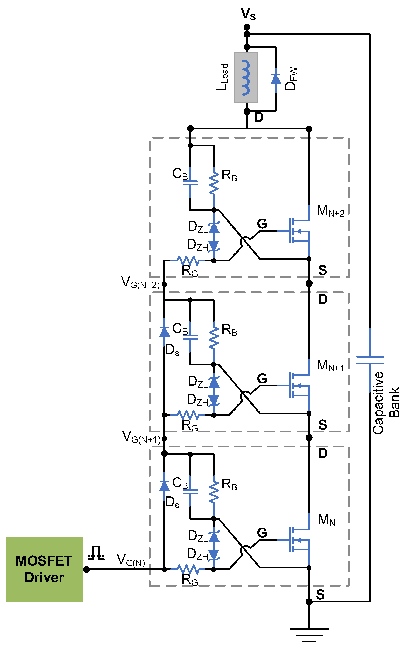
Figure 1 shows the proposed basic driving cell for a SiC MOSFET that can be cascaded with other cells to drive series SiC MOSFETs. As shown in the figure, the circuit consists of basic passive components (2 resistors, 1 diode, 2 Zener diodes, and 1 capacitor) that provide reliability to the design against variations in temperature, frequency, and voltages spikes and do not include magnetic components that might produce EMI issues and add complexity. The footprint and selection of these components could be optimized to achieve a compact design. Figure 2 shows how three SiC MOSFETs can be driven by the cell. Each cell can provide bipolar driving, gate protection, and on- and off- state voltage balancing. The operation principle is described as follows:
2.1. Off-Steady-State Operation
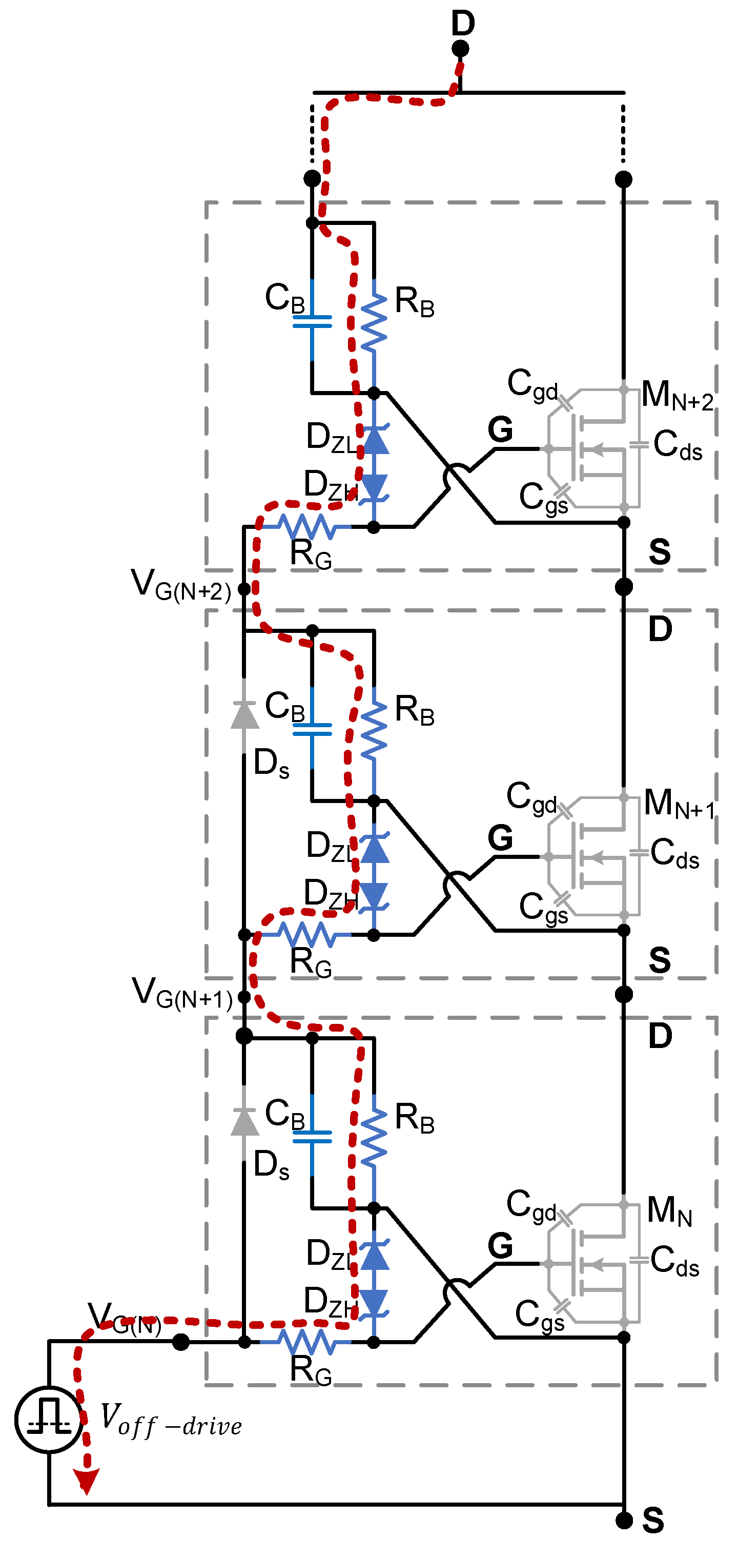
Threshold voltages are lower in SiC MOSFETs compared to silicon MOSFETs and IGBTs due to their incomplete p-type dopant post-anneal activation. For dopants to become active, they must ionize and either donate their valence electrons (for n-type doping) or accept electrons (for p-type doping). The wide bandgap characteristics of SiCs make this difficult for p-type dopants. Since p-body doping is proportional to the threshold voltage, this causes a lower threshold voltage. A negative gate-drive voltage is recommended to achieve a stable and reliable off-state in SiC MOSFETs and prevent a false turn-on. In the proposed design, the supply voltage was used to bias the Zener diodes, which resulted in a negative voltage, which was, in our case, −5 V. Figure 3 shows the driving cell for two SiC MOSFETs during the off-state where is the order of the MOSFET.
To bias the Zener diodes, a minimum current should pass through the network. Each cell has two resistors () and two Zener diodes (). In a proper steady state, one will be forward biased while the other is reversed, resulting in a gate–source voltage as follows:
For number of series MOSFETs, should follow:
MOSFETs have different values of leakage currents, , even when they are forced to have a similar balanced . To make the design robust against the uncertainty of leakage current, the was set as,
In case of dissimilarities of of MOSFETs [7], and by considering the worst case of one having and the other having as a maximum from the datasheet, then the will be between . For our experimental tested SiC MOSFET in this paper, SCT20N120, the maximum leakage drain current was 100 µA. So, the design oriented to be 1 mA, which is enough the bias the Vishay Zener diodes BZX55 series [23]. The maximum number of series MOSFETs can be obtained from (4). as a function of other components values and as
From MOSFET 1 to , the voltage across each MOSFET, will equal
However, for the MOSFET ,
So, the maximum steady state imbalance between MOSFET and the other MOSFETs is
Because the design targets high-voltage applications using hundreds to thousands of volts, is considered to be negligible. Therefore, the maximum can be designed as
2.2. Turn-On Transition
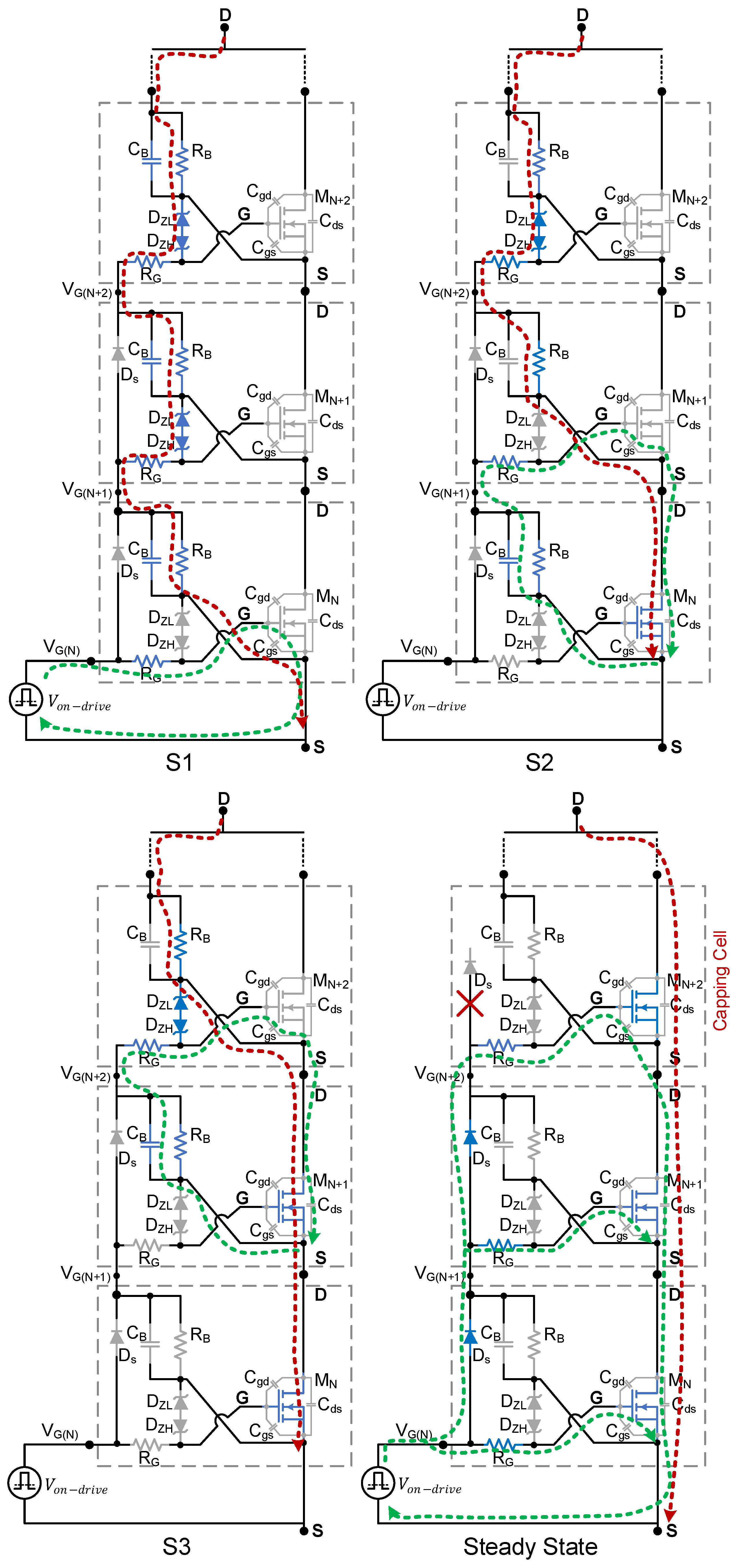
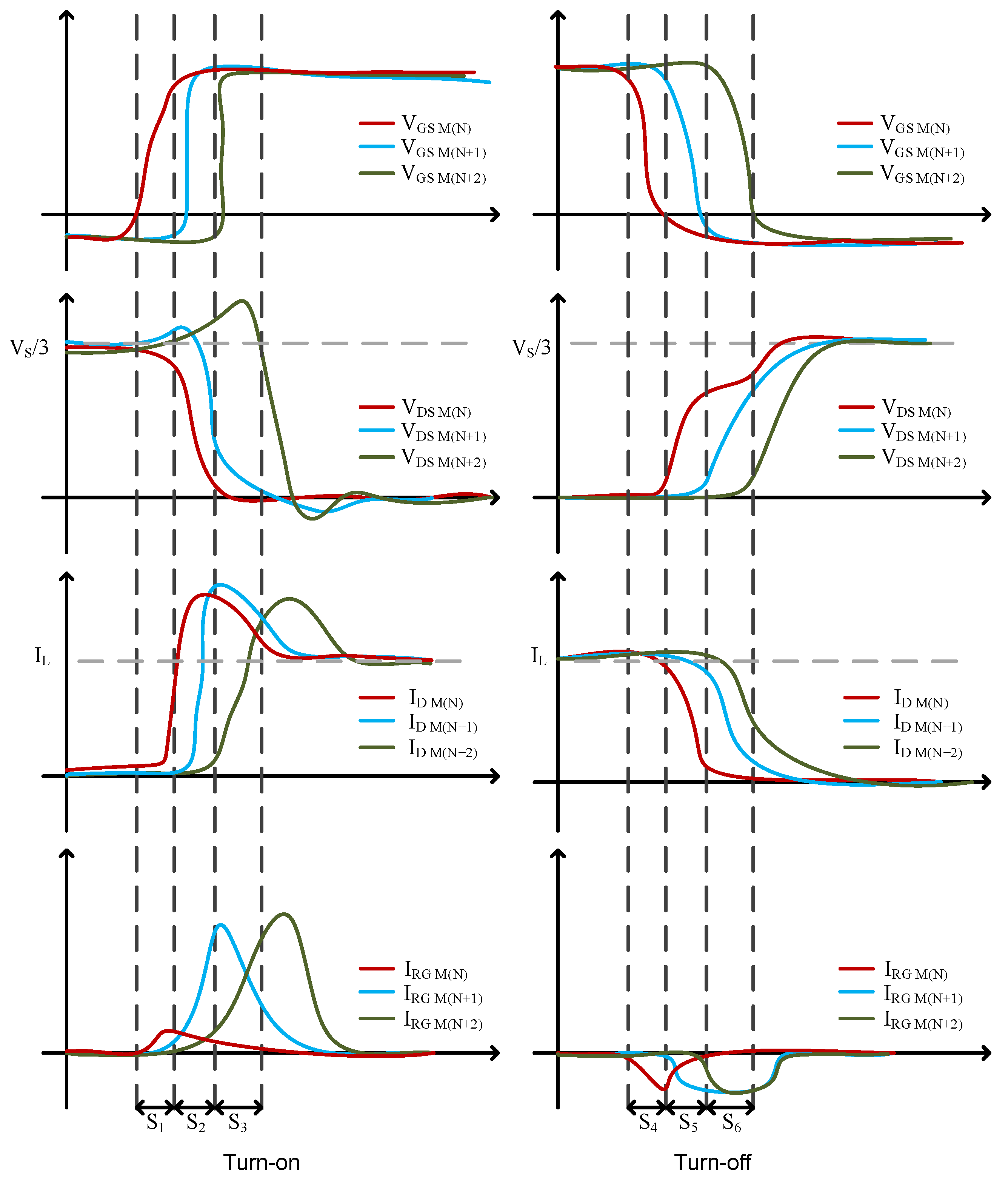
The analysis explained in this section for the voltage and current waveforms and switching transitions was based on a clamped inductive load in the commonly used double-pulse testing. Three SiC MOSFETs were assumed in this analysis to emphasize its modular operation if more MOSFETs are stacked. The turn-on transition is divided into three main stages. Figure 4 shows the current paths during the turn-on transition stages for the three MOSFETs. Figure 5 illustrates the gate-to-source voltage (), the drain-to-source voltage (), the drain currents (), and the gate resistance current () during the transition.
Stage 1 (S1): It was assumed that before this stage starts, all switches are off and the shared supply voltage is across each MOSFET and the is at a negative value. A turn-on signal is given by the gate driver to the first MOSFET, . The gate voltage starts rising, passing the threshold voltage while the MOSFETs are still in the off-state. The voltage across MOSFET , , is at a high voltage and the current is zero. The gate current is dominated by the current through the resistor and Figure 5 shows the current , which follows Equation (9).
The diode is in the off-state as the voltage across the is still higher than the drive voltage. The Zener diodes also will not operate as the drive voltage is lower than the protection threshold (+22 V).
Stage 2 (S2): At the beginning of stage 2, the current starts to rise while the voltage of MOSFET starts to fall, bringing the source node of MOSFET to a lower voltage than the drain node, which is illustrated by an overshoot of its voltage . The maximum volage can be estimated as
where
At the same time, the capacitor will have a new current path to discharge through the gate-to-source capacitance of , allowing to rise followed by a rise in its current and a fall in its voltage . The discharging current of capacitor is determined by the change in voltage at the source node of caused by the and the gate capacitance charge of , in addition to the value of . A basic illustration of the discharging circuit is shown in Figure 6. The peak current through can be calculated by Equation (12) with the assumption of the worst case of a complete change in from to zero.
where is the turn-on switching time and is the number of MOSFETs. Obviously, a larger produces a higher peak current, which is required for charging in a fast manner. However, large capacitance leads to a longer time to balance the voltages at the off-state and reach a steady state. Furthermore, it increases the switching loss when its cell MOSFET is on through its .
Stage 3 (S3): Similar to stage 2, when MOSFET is turned on, the voltage at the source node of drops. Consequently, the capacitor discharges and the time constant is determined by the value of the path capacitances, and . Larger values of and increase the time of discharge, keep steadier and dissipate less power, but this will disturb the turn-off operation dynamics.
At steady state and when all MOSFETs are on, diode is used to prevent from dropping because its gate capacitances will discharge through and . Therefore, keeps supplying a minimal steady state current. A similar case is for in keeping at sufficient gate voltage level. The current through the diode in each cell () is calculated based on Equation (13)
where is the forward voltage drop across the diode . Larger capacitance provides a steadier , but it will deteriorate the turn-off time.
As is shown in Figure 4, the last driving cell for has no supply diode because it will create a current path from the driver through to the top drain node, which has a low voltage due to the MOSFETs being on. This will draw a significant current and decrease the capability of the driver to keep all MOSFETs at the on-state properly. For this reason, a “Capping Cell” was proposed, which has the same structure but with no supply diode.
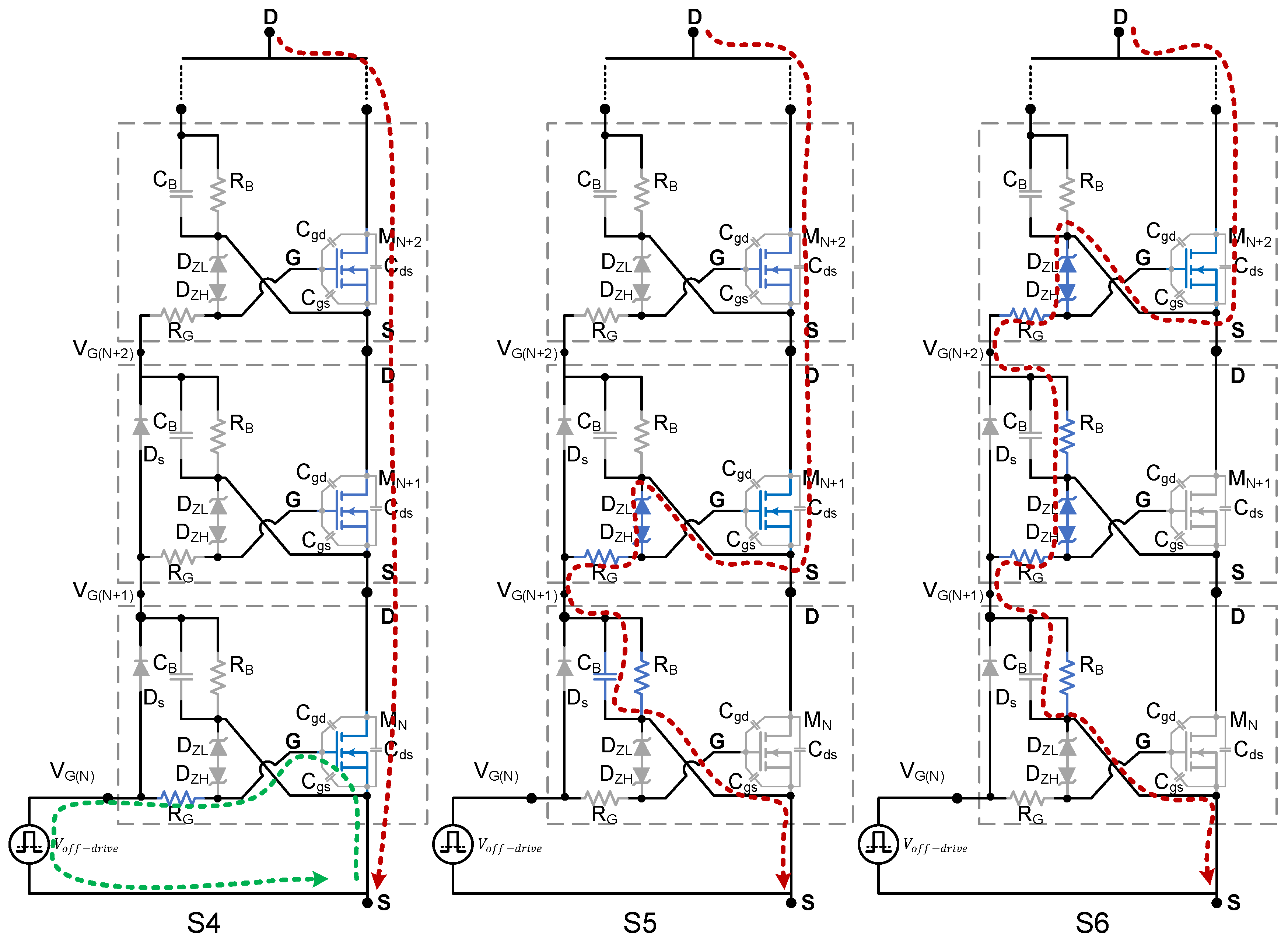
2.3. Turn-Off Transition
Figure 5 shows the transition during the turn-off, and it is divided into three stages. Similarly, the current paths during each stage are shown in Figure 7.
Stage 4 (S4): Before this stage, it was assumed that all MOSFETs are in an on steady state and they are conducting the current from the top drain node to the bottom source node through their on-state resistances. At this stage, a negative driving voltage is generated by the driver, and is discharging the gate capacitance through . The current through the resistance is as follows.
where is the initial voltage across the gate–source of MOSFET . While the current rises, as shown in Figure 5, the gate voltage drops.
Stage 5 (S5): The gate voltage drops to a level below the threshold voltage and the voltage starts rising while the current starts dropping, turning off MOSFET completely. The through MOSFETs and is commutated through the Zener diodes , the gate resistance , and the balance resistance to the source terminal, as shown in Figure 7. This current will charge , making the voltage across the MOSFET increase slowly to realize ZCS. This current will also bias the Zener diode to produce a negative voltage equal to across the . The applied voltage will start turning off the MOSFET. It is worth mentioning here that should be selected to pass the minimum Zener current, . It is important to keep the switching time as short as possible to avoid higher dissipation when flows through the Zener diodes.
Stage 6 (S6): Similar to S5, after turning off MOSFET, the current passes through a series of Zener diodes, ’s and ’s, to the source node as shown in Figure 7. This will bias the Zener diode to turn off the MOSFET. Here, the combination of ’s should be able to pass the through all Zener diodes. The balance capacitors achieve turn-off soft switching, which is crucial for applications such as SSCBs.
3. Parameter Calculations
3.1. Parameter Calculation of
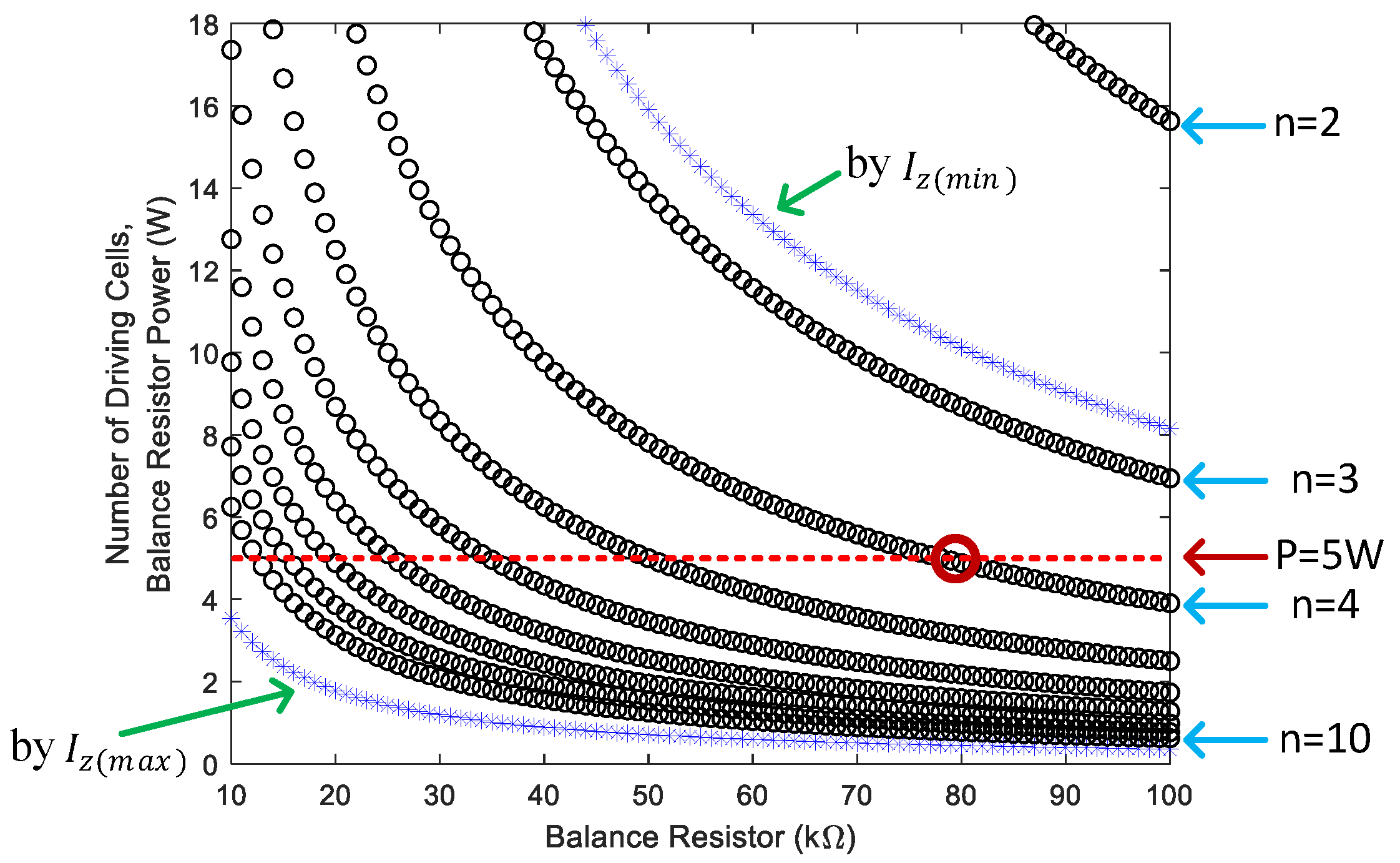
As shown in Equation (8), is responsible for proper Zener diode biasing during the turn-off transition. A large value of limits the number of stacked SiC MOSFETs in series due to inability to bias the Zener diodes for a particular source voltage. A small value of limits the number of stacked SiC MOSFETs in series due to the significant power dissipation at the off steady state if a high voltage is present across . Figure 8 shows combined plots for the limitations brought by the Zener diode currents and on the number of stacked MOSFETs when . In addition, it shows the power dissipation brought by a resistor value for different numbers of stacked MOSFETs when . The selected source voltage for these calculations was . Obviously, at least four stages, , are required to fulfil the Zener diodes biasing requirements. It is important to assume that four MOSFETs have a total rating more than the operating . Otherwise, more cells are required. In our example, each MOSFET had a maximum voltage of 1200 V and in total, this was . If 5 W is selected as an example of a maximum resistor power in the design due to size considerations, the red line in Figure 8 depicts the resistor values limits and shows that the best resistor value, denoted by the red circle, for the least number of stages, was with .
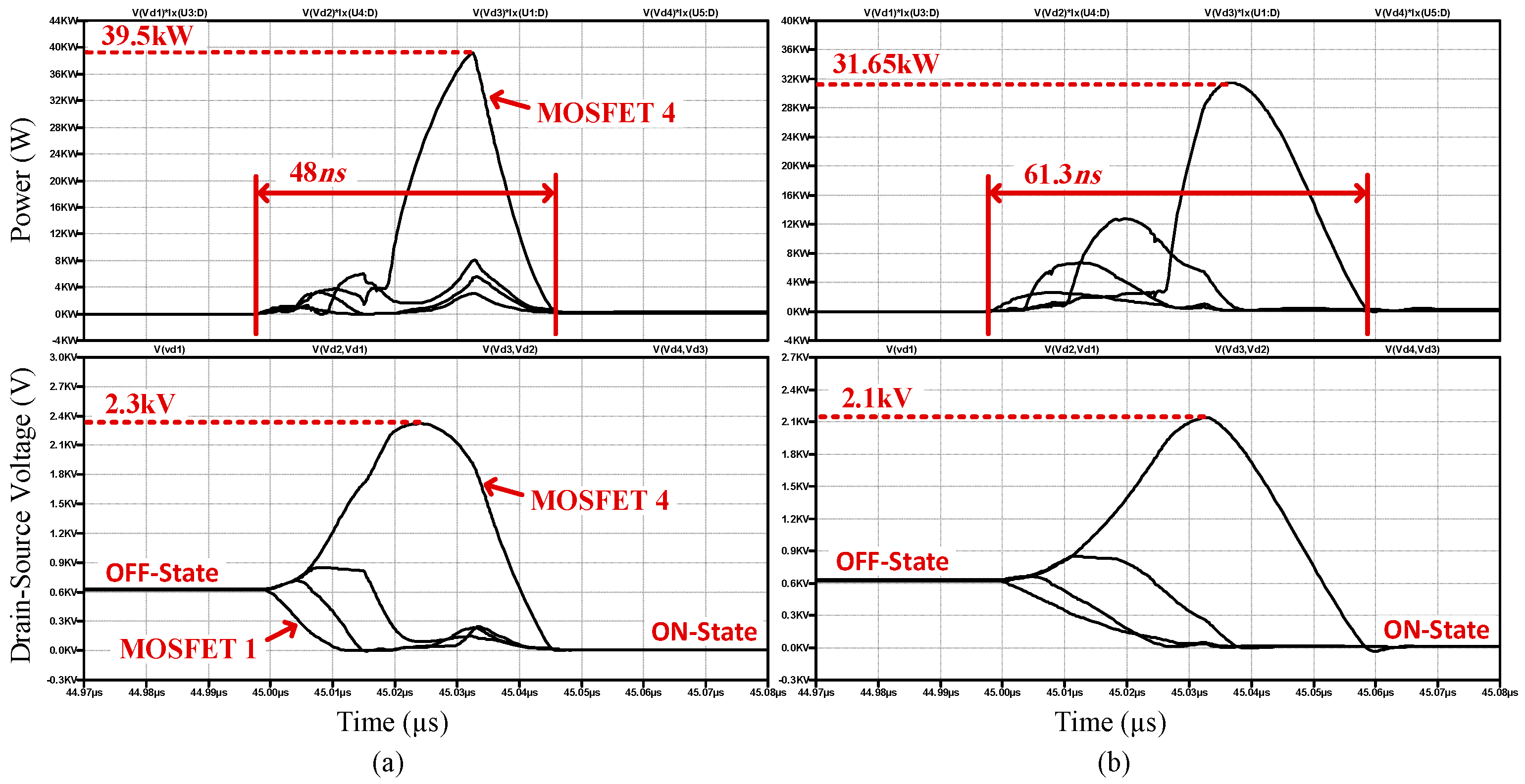
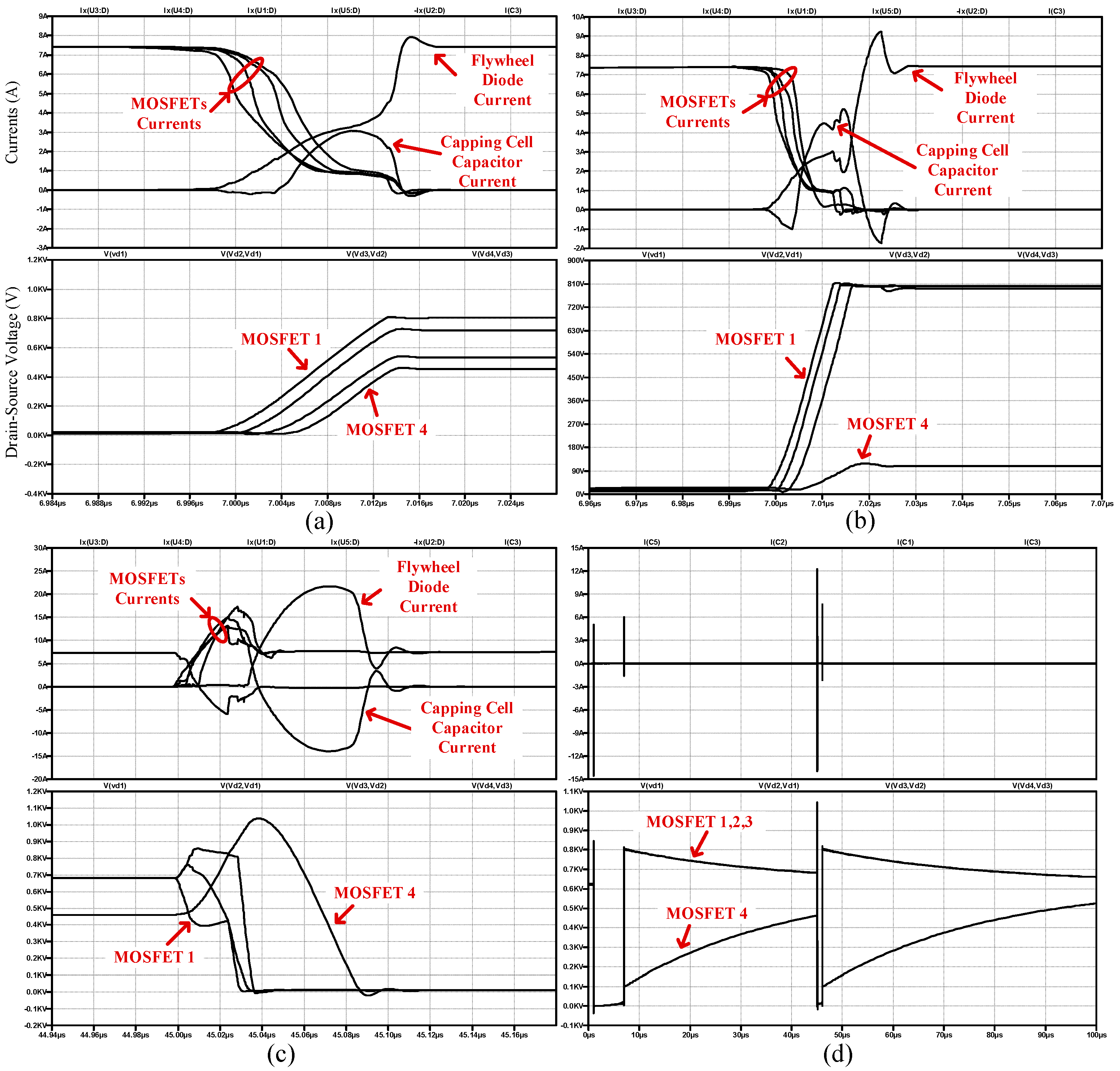
A simulation was conducted for and being set to three different values and the turn-on and turn-off times for each MOSFET were measured and are listed in Table 1. For the tested case, the impact of on the and was negligible. However, it significantly increased the steady state off-time when increased. Figure 9 shows the instantaneous power and voltage waveforms during the turn-off transition when . The total turn-off time was slightly affected but the power peak increased from , which increased the total energy loss.
3.2. Parameter Calculation of
As discussed previously, is responsible for charging the next stage MOSFET gate, and the dynamics of charging the gate of MOSFET is dominated by the turn-on transition of MOSFET and how the voltage at the drain node drops to the source node. Large values will delay the MOSFETs in balancing the supply voltage when they are turned off. In addition, this increases the switching time and losses.
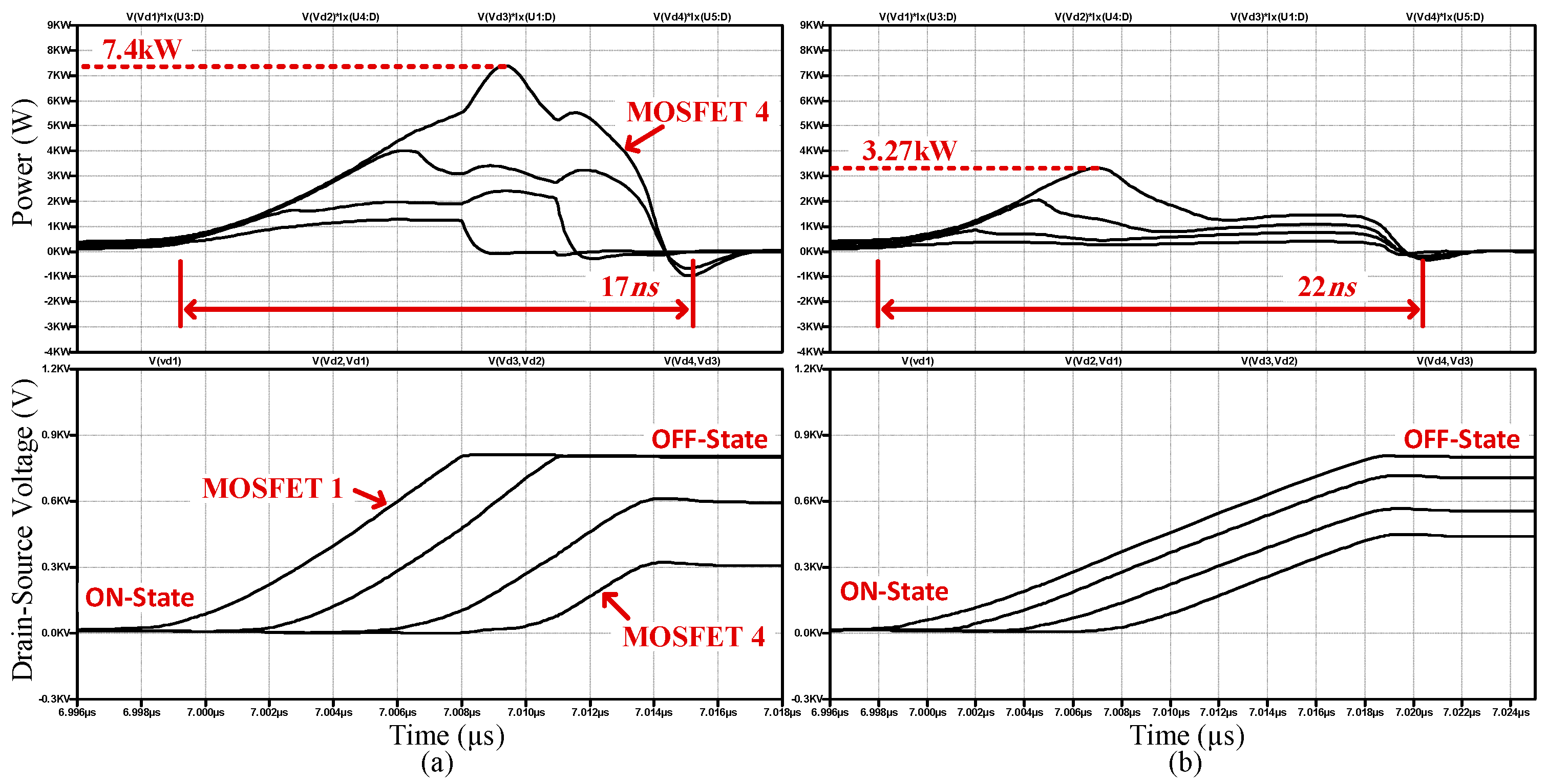
Table 2 shows how higher values increased the steady state time at the off-state. It increased the turn-on time by 45% and the turn-off time by 100%. The value of provided the shortest time. However, even with a shorter on-transition, the instantaneous power and waveforms had high peaks during the on-transition, as shown in Figure 10, which might exceed the MOSFET rating and incur a high value of . The top device needs to be avalanche-rugged to withstand this voltage and additional losses from repetitive avalanches might break it down. During turn-off, the was the highest because it had a high instantaneous power peak, as shown in Figure 11. The figure also shows the non-uniform voltage dynamics compared with the case of , where less power peaks, uniform dynamics among all MOSFETs and soft switching were achieved. Therefore, the selection of is a trade-off between the turn-on voltage overshoot, steady state and the switching loss.
It is worth mentioning that the peak voltage of MOSFET 4, in Figure 10, could be reduced significantly by selecting a higher value of compared with the other cells. This allowed a smoother turn-on for MOSFET 4 as the capacitor absorbed the load current while the voltage increased. Figure 12a shows the turn-on transition when for the M (N + 3) cell while keeping the others with a value of . The peak voltage was then within 1.1 kV. However, this sacrificed the settling time during the off-time as shown in Figure 12b and consequently the switching frequency. The designer might tailor this value according to the application.
3.3. Parameter Calculation of
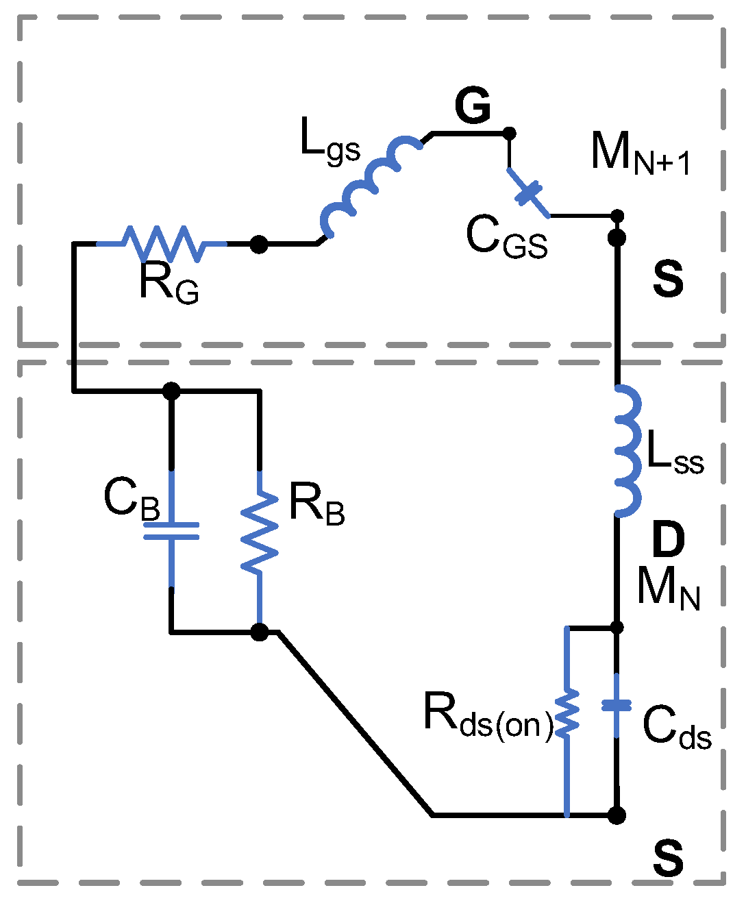
Figure 13 shows the inclusion of stray inductances within the driving circuit. represents the gate inductance induced by the printed circuit board tracks and terminal lengths. represents the lamped source and drain inductance of adjacent MOSFETs. The path capacitances and inductances will resonate if does not provide enough damping. By neglecting , due to its large value and because it is not a design parameter that can be fixed, and it is also very small, the damping factor of the circuit is:
To prevent oscillation, should be greater than 1, therefore, is selected to satisfy.
Furthermore, it is worth mentioning here that the value should not be selected to be large because it will increase the switching loss and slow down the MOSFET switching in addition to disturbing the Zener diode biasing at turn-off. Usually, resistors can withstand high peak currents for short times, i.e., during turn-off transitions.
3.4. Parameter Calculation of
The supply diodes provide a continuous charge for the balance capacitors during the turn-on steady state for all MOSFETs. In the proposed topology, the diodes are connected in series. Therefore, the final voltage at each cell drops with the increase in cell number. If we assume that each MOSFET needs at least to keep it in a proper conduction with minimal , then the maximum number of cascaded cells will follow:
where is the forward voltage drop across the supply diode. For the used diode in the experimental setup, i.e., the US1M diode, the voltage drop was 1.7 V at a current of 1 A and the for the MOSFET was 3.5 V and . Therefore, . By replacing the diode with a low voltage drop, the number of possible cascaded cells will increase.
4. Simulation Verification
LTspice was used to simulate three stacked MOSFETs in series. The modelled SiC MOSFET was C2M1000170D. Wolfspeed provided the spice model. A double-pulse test (DPT) with a clamped inductor load was simulated. The circuit is shown in Figure 14 and the simulation values are shown in Table 3. The source voltage was chosen to be to mimic the experimental setup, which had a maximum voltage of 350 V due to the available sources.
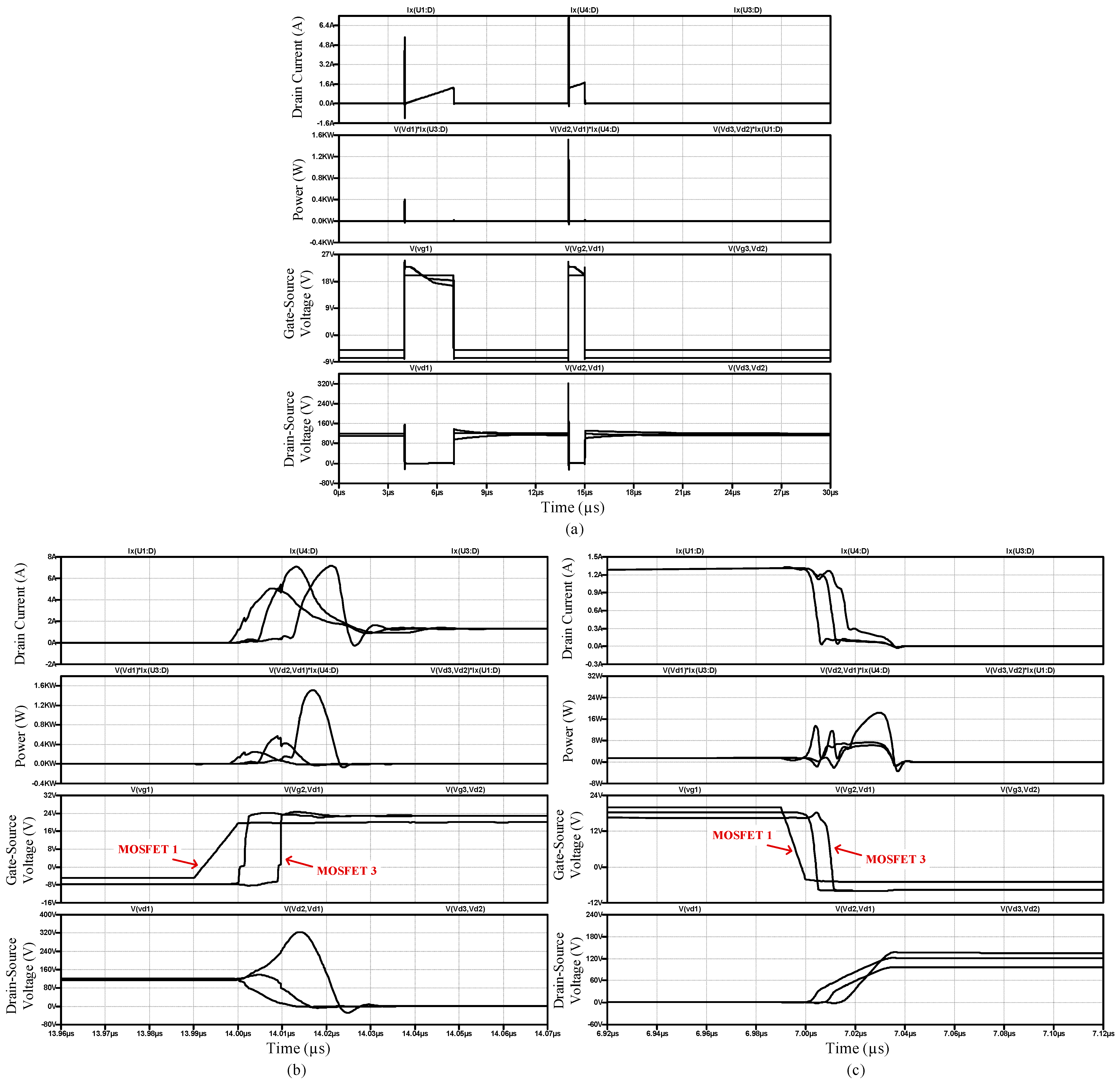
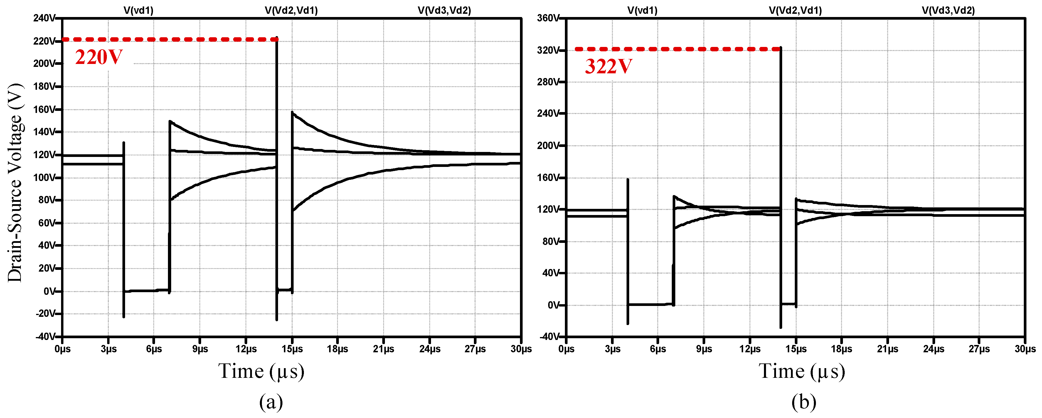
The DPT waveforms are shown in Figure 15 including the gate–source voltages, the drain–source voltages, drain currents, and instantaneous power. The results depicted a balanced voltage sharing at the off steady state. In addition, it showed consistent dynamics of voltage and current among all the MOSFETs. The maximum voltage during the turn-on transition was 320 V.
Figure 16 shows how the supply diodes shaped the gate voltages. Figure 16a is the normal proposed topology with populated supply diodes for each driving cell except the capping cell. The results in Figure 16b are shown for the design without any supply diodes. The balance capacitors kept discharging and this might have driven the MOSFETs to a linear region. Figure 16c is when the capping cell supply diode was populated, and it shows how the voltages were clipped differently with a difference between each cell equal to the Zener diode (6.8 V).
As shown and discussed, the single gate-drive approach proposed switches the series-connected SiC-MOSFETs in a sequential manner. To compensate for the transient switching speed differences among the individual SiC-MOSFETs, some adjustments to the values of auxiliary capacitors could be made.
Figure 17 shows how the capping cell-balance capacitor, , affected the transient time and the voltage peak. Figure 17a shows a similar balance capacitor for all cells (), while in Figure 17b, the capping cell capacitor is reduced alone to . A faster response was achieved but with a higher turn-on voltage peak for the MOSFET . The selection of also impacted the maximum switching frequency. Therefore, a trade-off should be considered here.
5. Experimental Results
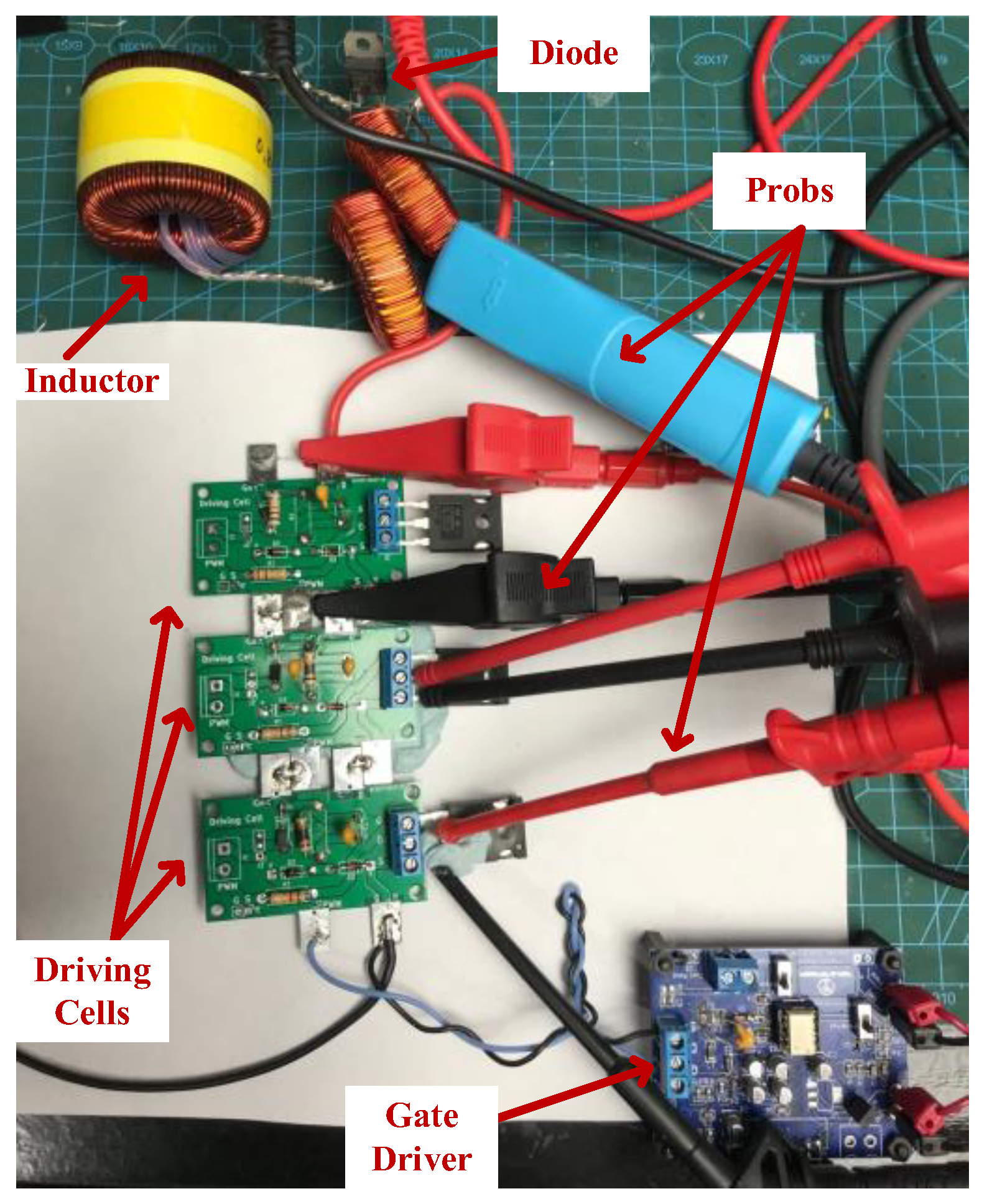
The proposed topology was built and tested experimentally to validate the design. The circuit was as shown in Figure 14, and the experimental setup is shown in Figure 18. The setup was composed of three series SCT20N120, 1200 V, 20 A MOSFETs. The conducted test was a DPT with a load inductance of 1800 µH and the freewheeling diode was a STPSC1206 Schottky silicon carbide diode. The PCB boards were designed in a modular manner and could be soldered together to stack different numbers of MOSFETs. The power supply was a 350 V DC source with a bulk capacitor array. The detailed experimental setup components are listed in Table 3. Micsig differential voltage and current probes were used with a 100 MHz bandwidth. The DPT signals were produced by a microcontroller.
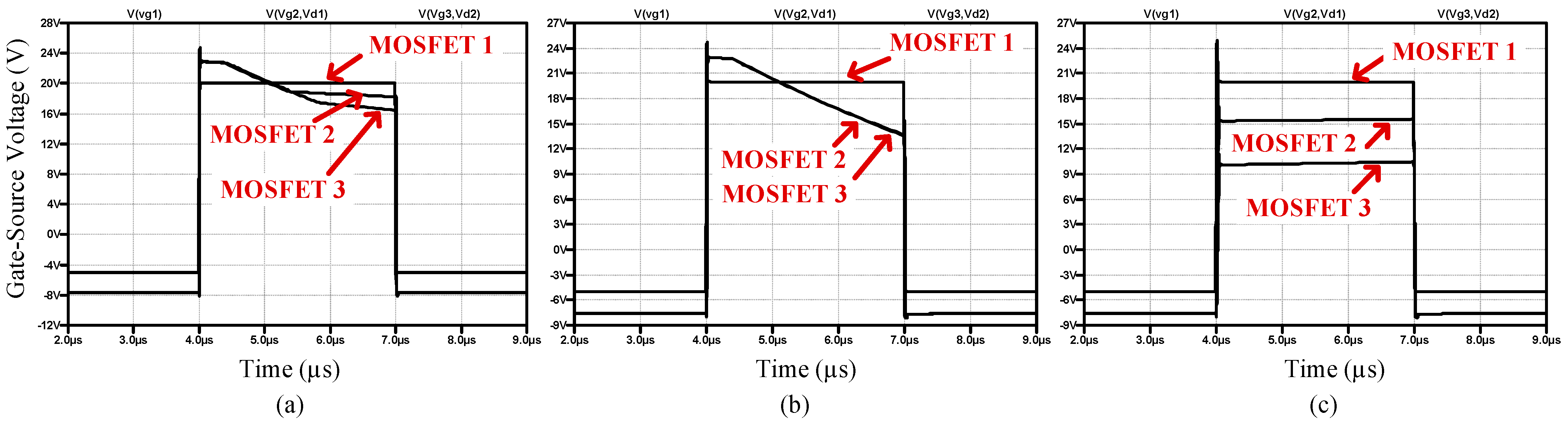
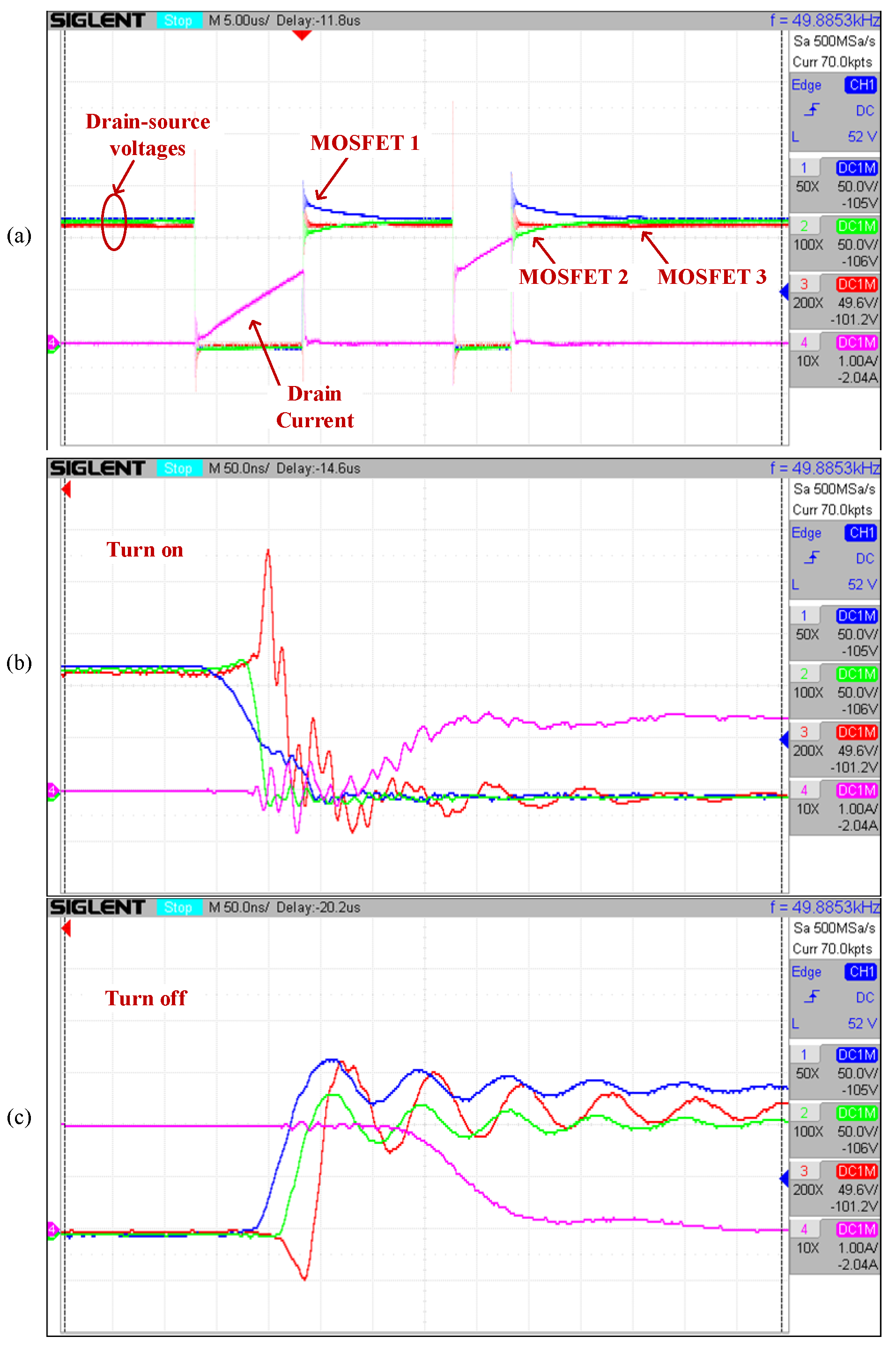
Figure 19a shows the experimental results for the DPT. Obviously, the proposed circuit was able to turn on and off the three series MOSFETs successfully. Each MOSFET shared an almost equal voltage during the turn-off steady state. The differences were due to the voltage drop across the Zener diodes. The gate voltages were supplied by a negative voltage when they were off.
Figure 19b shows a zoomed-in view of the turn-on transition. The maximum voltage of MOSFET was 227 V, which was similar to the simulation results. The total turn-on transition was 96 ns, while the turn-off transition was 87 ns, as shown in Figure 19c. The oscillation was caused by the stray inductance. The results confirmed the analysis and design.
The main advantage of this gate-drive strategy is that a single gate driver is required to switch more than one device since the energy stored in the balance capacitors are used to charge and discharge the gate capacitances in subsequent devices. This is unlike other designs that require each device in a series configuration to be driven by a dedicated gate driver. The design also provides flexibility in mitigating higher voltage stresses on MOSFETs by the proper selection of the switching capacitors.
The voltage blocked for each device will be, as a maximum, the ratio of the DC link voltage and the number of devices . The ratio of this voltage to the intrinsic breakdown voltage of the device will determine the headroom for each device and, hence, the additional voltage each device can block under voltage imbalance conditions. If a small capacitor is used for the capping cell, more MOSFETs can be considered to further distribute the switched voltage while switching.
6. Conclusions
In this paper, a modular switching capacitor-based driving cell was proposed to drive series SiC MOSFETs. The proposed circuit did not require any active components and could be driven by a single gate driver. The proposed driving cells were able to provide negative voltages during the off-states and sufficient charge during the on-transition. The analysis of the proposed topology validated its modular aspects and highlighted its limitations and criteria of component selection. The balance capacitor was key for the settling time and voltage overshoot adjustments. LTspice simulations for three and four MOSFETs were conducted. The experimental prototype for three MOSFETs in series approved the validity of the design with a less than 100 ns transition and coherent switching. The potential of this topology can be applicable for high-voltage circuit breakers and high-stressed MOSFETs in power supplies.
Author Contributions
Conceptualization, W.I.; methodology, W.I.; formal analysis, J.O.G.; investigation, O.A.; resources, W.I.; writing—original draft preparation, W.I.; writing—review and editing, J.O.G. and O.A.; visualization, W.I. All authors have read and agreed to the published version of the manuscript.
Funding
This research received no external funding.
Institutional Review Board Statement
Not applicable.
Informed Consent Statement
Not applicable.
Data Availability Statement
Not applicable.
Acknowledgments
For the purpose of open access, the author has applied a Creative Commons Attribution (CC BY) license to any author-accepted manuscript version arising from this submission.
Conflicts of Interest
The authors declare no conflict of interest.
References
- Millan, J.; Godignon, P.; Perpina, X.; Perez-Tomas, A.; Rebollo, J. A Survey of Wide Bandgap Power Semiconductor Devices. IEEE Trans. Power Electron. 2013, 29, 2155–2163. [Google Scholar] [CrossRef]
- Hazra, S.; De, A.; Cheng, L.; Palmour, J.; Schupbach, M.; Hull, B.A.; Allen, S.; Bhattacharya, S. High Switching Performance of 1700 V, 50 A SiC Power MOSFET over Si IGBT/BiMOSFET for Advanced Power Conversion Applications. IEEE Trans. Power Electron. 2015, 31, 4742–4754. [Google Scholar] [CrossRef]
- Mainali, K.; Tripathi, A.; Madhusoodhanan, S.; Kadavelugu, A.; Patel, D.; Hazra, S.; Hatua, K.; Bhattacharya, S. A Transformerless Intelligent Power Substation: A three-phase SST enabled by a 15-kV SiC IGBT. IEEE Power Electron. Mag. 2015, 2, 31–43. [Google Scholar] [CrossRef]
- Eni, E.-P.; Kerekes, T.; Uhrenfeldt, C.; Teodorescu, R.; Munk-Nielsen, S. Design of low impedance busbar for 10 kV, 100 A 4H-SiC MOSFET short-circuit tester using axial capacitors. In Proceedings of the 2015 IEEE 6th International Symposium on Power Electronics for Distributed Generation Systems (PEDG), Aachen, Germany, 22–25 June 2015. [Google Scholar] [CrossRef]
- Bolotnikov, A.; Losee, P.; Permuy, A.; Dunne, G.; Kennerly, S.; Rowden, B.; Nasadoski, J.; Harfman-Todorovic, M.; Raju, R.; Tao, F.; et al. Overview of 1.2 kV–2.2 kV SiC MOSFETs targeted for industrial power conversion applications. In Proceedings of the 2015 IEEE Applied Power Electronics Conference and Exposition (APEC), Charlotte, NC, USA, 15–19 March 2015; pp. 2445–2452. [Google Scholar] [CrossRef]
- Ji, S.; Lu, T.; Zhao, Z.; Yu, H.; Yuan, L. Series-Connected HV-IGBTs Using Active Voltage Balancing Control With Status Feedback Circuit. IEEE Trans. Power Electron. 2014, 30, 4165–4174. [Google Scholar] [CrossRef]
- Ren, Y.; Yang, X.; Zhang, F.; Wang, K.; Chen, W.; Wang, L.; Pei, Y. A Compact Gate Control and Voltage-Balancing Circuit for Series-Connected SiC MOSFETs and Its Application in a DC Breaker. IEEE Trans. Ind. Electron. 2017, 64, 8299–8309. [Google Scholar] [CrossRef]
- Wu, X.; Cheng, S.; Xiao, Q.; Sheng, K. A 3600 V/80 A Series--Parallel-Connected Silicon Carbide MOSFETs Module With a Single External Gate Driver. IEEE Trans. Power Electron. 2013, 29, 2296–2306. [Google Scholar] [CrossRef]
- Hess, H.L.; Baker, R.J.J. Transformerless capacitive coupling of gate signals for series operation of power MOS devices. IEEE Trans. Power Electron. 2000, 15, 923–930. [Google Scholar] [CrossRef] [Green Version]
- Grbovic, P.J. High-Voltage Auxiliary Power Supply Using Series-Connected MOSFETs and Floating Self-Driving Technique. IEEE Trans. Ind. Electron. 2009, 56, 1446–1455. [Google Scholar] [CrossRef]
- Grbovic, P. Loss-Free Balancing Circuit for Series Connection of Electrolytic Capacitors Using an Auxiliary Switch-Mode Power Supply. IEEE Trans. Power Electron. 2009, 24, 221–231. [Google Scholar] [CrossRef]
- Yang, C.; Pei, Y.; Xu, Y.; Zhang, F.; Wang, L.; Zhu, M.; Yu, L. A Gate Drive Circuit and Dynamic Voltage Balancing Control Method Suitable for Series-Connected SiC mosfets. IEEE Trans. Power Electron. 2019, 35, 6625–6635. [Google Scholar] [CrossRef]
- Lim, T.C.; Williams, B.W.; Finney, S.J.; Palmer, P.R. Series-Connected IGBTs Using Active Voltage Control Technique. IEEE Trans. Power Electron. 2012, 28, 4083–4103. [Google Scholar] [CrossRef]
- Withanage, R.; Shammas, N. Series Connection of Insulated Gate Bipolar Transistors (IGBTs). IEEE Trans. Power Electron. 2011, 27, 2204–2212. [Google Scholar] [CrossRef]
- Zhang, F.; Yang, X.; Chen, W.; Wang, L. Voltage Balancing Control of Series-Connected SiC MOSFETs by Using Energy Recovery Snubber Circuits. IEEE Trans. Power Electron. 2020, 35, 10200–10212. [Google Scholar] [CrossRef]
- Zhang, F.; Yang, X.; Ren, Y.; Feng, L.; Chen, W.; Pei, Y. A Hybrid Active Gate Drive for Switching Loss Reduction and Voltage Balancing of Series-Connected IGBTs. IEEE Trans. Power Electron. 2016, 32, 7469–7481. [Google Scholar] [CrossRef]
- Teerakawanich, N.; Johnson, M. Design Optimization of Quasi-Active Gate Control for Series-Connected Power Devices. IEEE Trans. Power Electron. 2013, 29, 2705–2714. [Google Scholar] [CrossRef]
- Ren, Y.; Yang, X.; Zhang, F.; Wang, F.; Tolbert, L.M.; Pei, Y. A Single Gate Driver Based Solid-State Circuit Breaker Using Series Connected SiC MOSFETs. IEEE Trans. Power Electron. 2018, 34, 2002–2006. [Google Scholar] [CrossRef]
- Ren, Y.; Yang, X.; Zhang, F.; Chen, W. Analysis of series SiC MOSFETs stack using a single standard gate driver. In Proceedings of the 2016 IEEE 8th International Power Electronics and Motion Control Conference (IPEMC-ECCE Asia), Hefei, China, 22–26 May 2016; pp. 1664–1668. [Google Scholar] [CrossRef]
- Alves, L.F.S.; Lefranc, P.; Jeannin, P.-O.; Sarrazin, B. Review on SiC-MOSFET devices and associated gate drivers. In Proceedings of the IEEE International Conference on Industrial Technology, Lyon, France, 20–22 February 2018; pp. 824–829. [Google Scholar] [CrossRef]
- Batard, C.; Ginot, N.; Bouguet, C. Design of a gate driver for SiC MOSFET module for applications up to 1200 V. IET Power Electron. 2020, 13, 1364–1373. [Google Scholar] [CrossRef]
- Kumar, A.; Losito, M.; Moradpour, M.; Gatto, G. Current Source Gate Driver for SiC MOSFETs in Power Electronics Applications. In Proceedings of the 2022 International Symposium on Power Electronics, Electrical Drives, Automation and Motion, SPEEDAM 2022, Sorrento, Italy, 22–24 June 2022; pp. 523–527. [Google Scholar] [CrossRef]
- BZX55-Series Vishay Semiconductors Small Signal Zener Diodes. Available online: https://www.vishay.com/docs/85604/bzx55.pdf (accessed on 19 September 2022).
Figure 1.
Proposed driving cell.

Figure 2.
Cascaded driving cells.

Figure 3.
Off-steady-state. The arrow illustrates the current flow while all MOSFETs are off.

Figure 4.
Main current paths during turn-on while the circuit transitions from stage 1 (S1) to steady state. Red path denotes the drain current and green path denotes the gate–source current.
Figure 4.
Main current paths during turn-on while the circuit transitions from stage 1 (S1) to steady state. Red path denotes the drain current and green path denotes the gate–source current.

Figure 5.
Analytical waveforms during turn-on and turn-off transitions.

Figure 6.
Discharging circuit to turn on MOSFET M (N + 1).

Figure 7.
Main current paths during turn-off.

Figure 8.
Balance resistor in relation with and .

Figure 9.
The simulated instantaneous power and voltage waveforms during turn-off transition when (a) and (b) .
Figure 9.
The simulated instantaneous power and voltage waveforms during turn-off transition when (a) and (b) .

Figure 10.
Simulated instantaneous power and voltage waveforms during turn-on transition when and (a) , (b) .
Figure 10.
Simulated instantaneous power and voltage waveforms during turn-on transition when and (a) , (b) .

Figure 11.
Simulated instantaneous power and voltage waveforms during turn-off transition when and (a) , (b) .
Figure 11.
Simulated instantaneous power and voltage waveforms during turn-off transition when and (a) , (b) .

Figure 12.
Simulated MOSFETs voltages and capping capacitor current when (a) and for the capping cell, (b–d) for the capping cell.
Figure 12.
Simulated MOSFETs voltages and capping capacitor current when (a) and for the capping cell, (b–d) for the capping cell.

Figure 13.
The stray inductances in the driving circuit.

Figure 14.
The proposed topology for simulation and experimental testing.

Figure 15.
Simulation results: (a) DPT simulation, (b) turn-on zoom, and (c) turn-off zoom.

Figure 16.
Gate–source voltage when supply diodes: (a) are populated except the last cell, (b) are not populated, and (c) are populated for all cells.
Figure 16.
Gate–source voltage when supply diodes: (a) are populated except the last cell, (b) are not populated, and (c) are populated for all cells.

Figure 17.
Drain-to-source voltage during the DPT when (a) and (b) .

Figure 18.
Experimental setup.

Figure 19.
Experimental results: (a) DPT test, (b) turn-on zoom, and (c) turn-off zoom.


Table 1.
Impact of changing .
Table 2.
Impact of changing .
Table 3.
Parameters for the tested setup.
| Component | Value | Component | Value |
|---|---|---|---|
| 1200 V | 6.8 V | ||
| 1800 µH | 22 V | ||
| STPSC1206 | US1M ULTRA-FAST 700 V, 1 A | ||
| 300 pF | 1.5 Ω | ||
| 10 kΩ | MOSFETs | SCT20N120 SiC |
Publisher’s Note: MDPI stays neutral with regard to jurisdictional claims in published maps and institutional affiliations. |
© 2022 by the authors. Licensee MDPI, Basel, Switzerland. This article is an open access article distributed under the terms and conditions of the Creative Commons Attribution (CC BY) license (https://creativecommons.org/licenses/by/4.0/).
Share and Cite
MDPI and ACS Style
Issa, W.; Ortiz Gonzalez, J.; Alatise, O. Design of a Gate-Driving Cell for Enabling Extended SiC MOSFET Voltage Blocking. Energies 2022, 15, 7768. https://doi.org/10.3390/en15207768
AMA Style
Issa W, Ortiz Gonzalez J, Alatise O. Design of a Gate-Driving Cell for Enabling Extended SiC MOSFET Voltage Blocking. Energies. 2022; 15(20):7768. https://doi.org/10.3390/en15207768
Chicago/Turabian StyleIssa, Walid, Jose Ortiz Gonzalez, and Olayiwola Alatise. 2022. "Design of a Gate-Driving Cell for Enabling Extended SiC MOSFET Voltage Blocking" Energies 15, no. 20: 7768. https://doi.org/10.3390/en15207768
Note that from the first issue of 2016, this journal uses article numbers instead of page numbers. See further details here.