
Fabrication of Flexible Quasi-Interdigitated Back-Contact Perovskite Solar Cells
by
 ,
,
Hryhorii P. Parkhomenko
1 ,
,
Erik O. Shalenov
1,2,
Zarina Umatova
1,
Karlygash N. Dzhumagulova
1,2 and
Askhat N. Jumabekov
1,*
1
Department of Physics, Nazarbayev University, Nur-Sultan 010000, Kazakhstan
2
Institute of Experimental and Theoretical Physics, Al-Farabi Kazakh National University, Almaty 050040, Kazakhstan
*
Author to whom correspondence should be addressed.
Energies 2022, 15(9), 3056; https://doi.org/10.3390/en15093056
Submission received: 2 March 2022
/
Revised: 16 March 2022
/
Accepted: 17 March 2022
/
Published: 21 April 2022
(This article belongs to the Topic Perovskites for Energy Applications)
Abstract
:Perovskites are a promising class of semiconductor materials, which are being studied intensively for their applications in emerging new flexible optoelectronic devices. In this paper, device manufacturing and characterization of quasi-interdigitated back-contact perovskite solar cells fabricated on flexible substrates are studied. The photovoltaic parameters of the prepared flexible quasi-interdigitated back-contact perovskite solar cells (FQIBC PSCs) are obtained for the front- and rear-side illumination options. The dependences of the device’s open-circuit potential and short-circuit current on the illumination intensity are investigated to determine the main recombination pathways in the devices. Spectral response analysis of the devices demonstrates that the optical transmission losses can be minimized when FQIBC PSCs are illuminated from the front-side. Optoelectronic simulations are used to rationalize the experimental results. It is determined that the obtained FQIBC PSCs have high surface recombination losses, which hinder the device performance. The findings demonstrate a process for the fabrication of flexible back-contact PSCs and provide some directions for device performance improvements.
1. Introduction
The use of photovoltaic (PV) technologies in producing clean and renewable energy is increasing at a fast pace [1]. In recent years, more and more countries have been trying to increase the percentage of energy production from the renewable sources [2]. At this moment, the most commonly used PV devices are silicon solar cells. However, the progression in improving the power conversion efficiencies (PCEs) of silicon solar cells is slow and somewhat stagnant [3,4].
Recently, new types of organic and organic–inorganic semiconductor materials have been actively researched [5]. One type of such materials is perovskites. Perovskites have found a wide range of applications in solar cells [6,7,8] and other optoelectronic devices [9,10,11]. This is due to their optimal optoelectronic properties such as tunable and direct bandgap [12,13] long charge carrier diffusion length [14] and high absorption coefficient [15]. In addition, the methods for producing thin films with perovskites are rather cheap and simple [16,17]. Nowadays, the PCEs of perovskite solar cells (PSCs) reached values as high as 25.5% and promise to increase further [18,19].
Currently, there is a fast-growing interest in developing flexible PV and other optoelectronic devices due to their lucrative application potential in wearable/portable electronics [20,21,22] and IoT technologies [23,24]. Due to this, perovskites, owing to their solution processability, low cost [25,26], and abundance, have been actively investigated for developing flexible PSCs [27,28]. In addition, the low-temperature processability coupled with the roll-to-roll manufacturing possibilities make it ideal for fabricating PSCs on plastic substrates such as polyethylene terephthalate (PET) [29,30] or polyethylene naphthalate (PEN) [31,32], which are low-cost, lightweight materials [31]. Currently, lab-scale flexible PSCs on PET substrates achieved PCEs as high as 21.1% and this is anticipated to increase further [33].
While the quest for new materials and the development of already known materials for optoelectronic applications continues, there is also a quest for new designs of solar cells. Quasi-interdigitated back-contact (QIBC) PSCs are devices with a novel and advanced device architecture [34,35,36]. The manufacturing principle of QIBC PSCs relies on performing the device electrodes on substrates, followed by deposition of the perovskite absorbing layer on top of the electrodes to complete the device fabrication process [34,37]. The idea of the proposed back-contact architecture is to illuminate QIBC PSCs directly from the perovskite side (front-side). In this case, the incident light directly enters the exposed perovskite photo-active layer [34]. This is in contrast to the typical planar PSCs with a sandwich architecture, in which some transmission losses occur as the incident light passes through the supporting substrate and device functional layers (transparent metallic layer and either electron- or hole-transporting layer (ETL or HTL)) before reaching the perovskite-absorbing layer [34,38]. Thus, the back-contact architecture for PSCs promises to improve the PCEs of devices even further by addressing the transmission loss issues [39].
Currently, a great deal of research efforts have been invested in developing flexible PSCs. However, very little work has been completed on developing flexible PSCs with back-contact architecture [40]. Therefore, in this work we demonstrate a fabrication method for flexible QIBC PSCs (hereon referred to as FQIBC PSCs) on PET substrates and conduct device characterization studies on the manufactured devices. The opto-electrical behavior of the FQIBC PSCs are studied at various light intensities using a current–voltage (J-V) measurement system; the spectral response of the devices are analyzed using an external quantum efficiency (EQE) measurement system. Theoretical modeling studies are used to rationalize the experimental findings and to provide an insight into the device physics of FQIBC PSCs.
2. Materials and Methods
2.1. Materials
PET substrates with the patterned indium tin oxide (ITO) layer (thickness: PET~125 μm, ITO~150 nm; sheet resistance: 48 Ω/sq) were purchased from Mekoprint. Photoresist AZ 1512 HS and developer AZ 726 MIF were purchased from Microchemicals GmbH. Lead (II) iodide (PbI2, 99.0%), N,N-dimethylformamide (DMF), and acetone were purchased from Sigma-Aldrich. Methylammonium iodide (MAI) (CH3NH3I, 99.99%) was purchased from Greatcell Energy.
2.2. Device Fabrication
To fabricate back-contact electrodes, first, the PET/ITO substrates are cleaned in a detergent water, deionized water, acetone, and ethanol for 15 min each while sonicating in an ultrasonic bath. Then, a 30 nm ZnO layer (serves as the ETL) is deposited on the freshly cleaned PET/ITO substrates using a radio frequency magnetron sputtering system (Model: Spectros, Kurt J. Lesker, Jefferson Hills, PA, USA). Afterwards, a polymer mask with the desired features for the second electrode is formed using photolithography tools. Here, a positive photoresist is deposited using a spin-coating method at 3000 rpm spinning speed and a spinning time of 30 s. After that, the substrates are placed on a hotplate for 2 min at 110 °C for baking. The final thickness of the photoresist after the baking step is ~1.5 μm. Then, the substrates with the photoresist layer are exposed to UV light (dose—370 mJ/cm2) through a photo-mask using the SUSS MicroTec MA/BA Gen4 mask aligner system. The UV-exposed areas of the photoresist are removed by washing the substrates in a developer solution (3:1 mix of AZ 726 MIF with water) for 90 s and subsequent rinsing with water.
The second electrode is formed on the substrates by sequential deposition of an Al2O3 insulating layer (thickness ~100 nm) and a gold layer (thickness ~70 nm) by reactive magnetron sputtering and thermal evaporation (Model: Mini SPECTROS, Kurt J. Lesker, Jefferson Hills, PA, USA), respectively. Here, the Al2O3 serves as a spacer between the cathode (ITO/ZnO) and the anode (gold) layers. A thin layer of chromium (~10 nm) is deposited between the gold and the Al2O3 layers via thermal evaporation to improve the adhesion of the gold layer to the Al2O3 insulating layer. Afterwards, the remains of the polymer mask are removed by washing the substrates in acetone to obtain the back-contact electrodes for FQIBC PSCs.
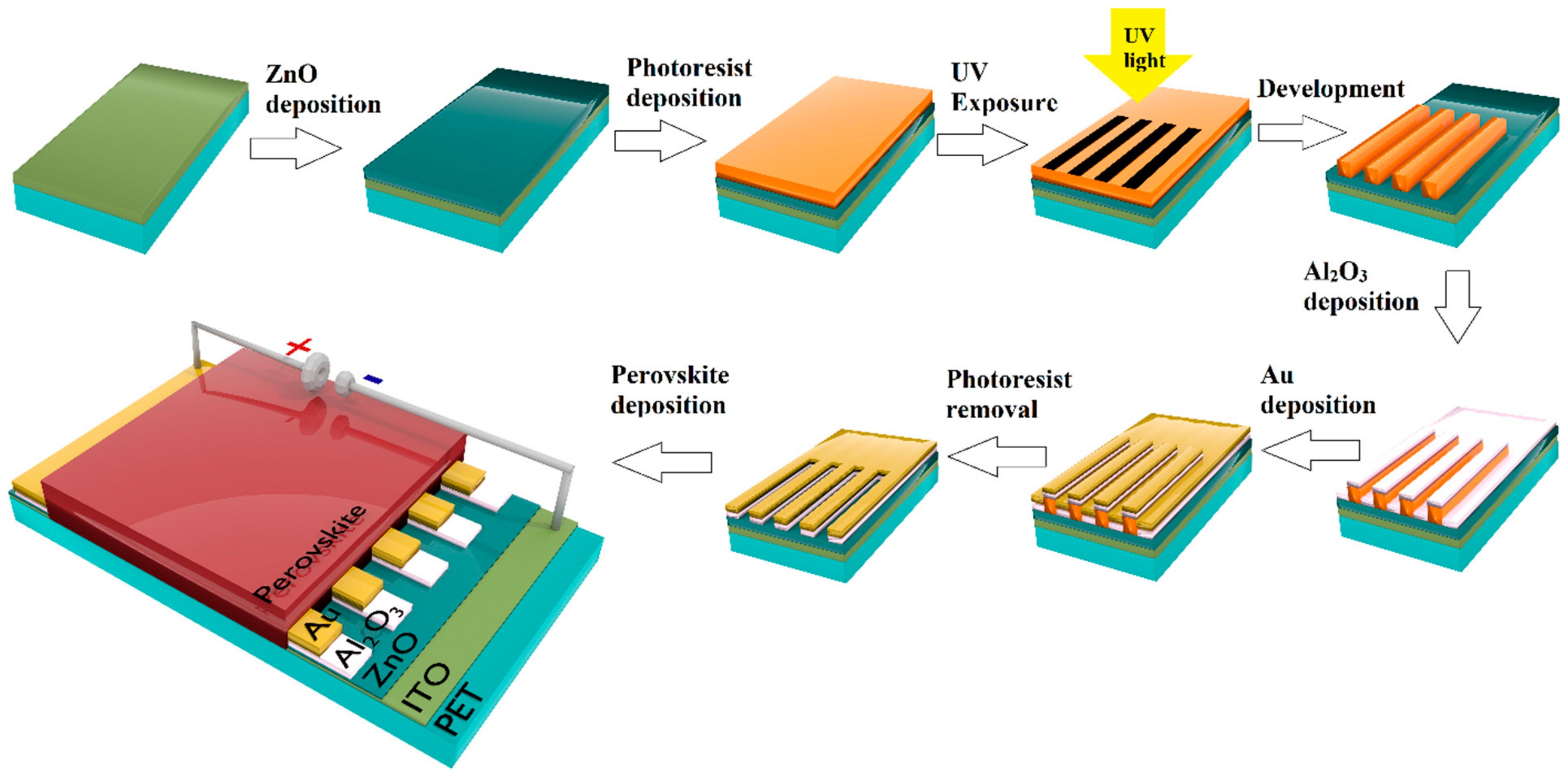
The last stage of the FQIBC PSC fabrication process is deposition of the perovskite photo-absorber layer. The precursor solution for the perovskite layer contains 0.461 g PbI2 and 0.159 g MAI in a 1:1 molar ratio and is dissolved in l mL of anhydrous DMF [41]. The perovskite layer is deposited onto the freshly prepared back-contact electrodes using a gas-assisted spin-coating method [42,43]. For this, 100 µL of the perovskite precursor solution is dropped onto the back-contact electrodes and spun for 30 s at 6500 rpm. After 2 s of spinning, the substrates are blown with a stream of nitrogen (pressure: 150 kPa) for 28 s using a nitrogen gun. The distance between the substrate and the nitrogen gun is ~10 cm. Once the spin-coating process is complete, the substrates are annealed at 100 °C on a hotplate for 15 min. This affords the formation of a crystalline CH3NH3PbI3 perovskite photo-absorber layer. The schematic representation of the device fabrication process and schematic diagram of the final device are shown in Figure 1.
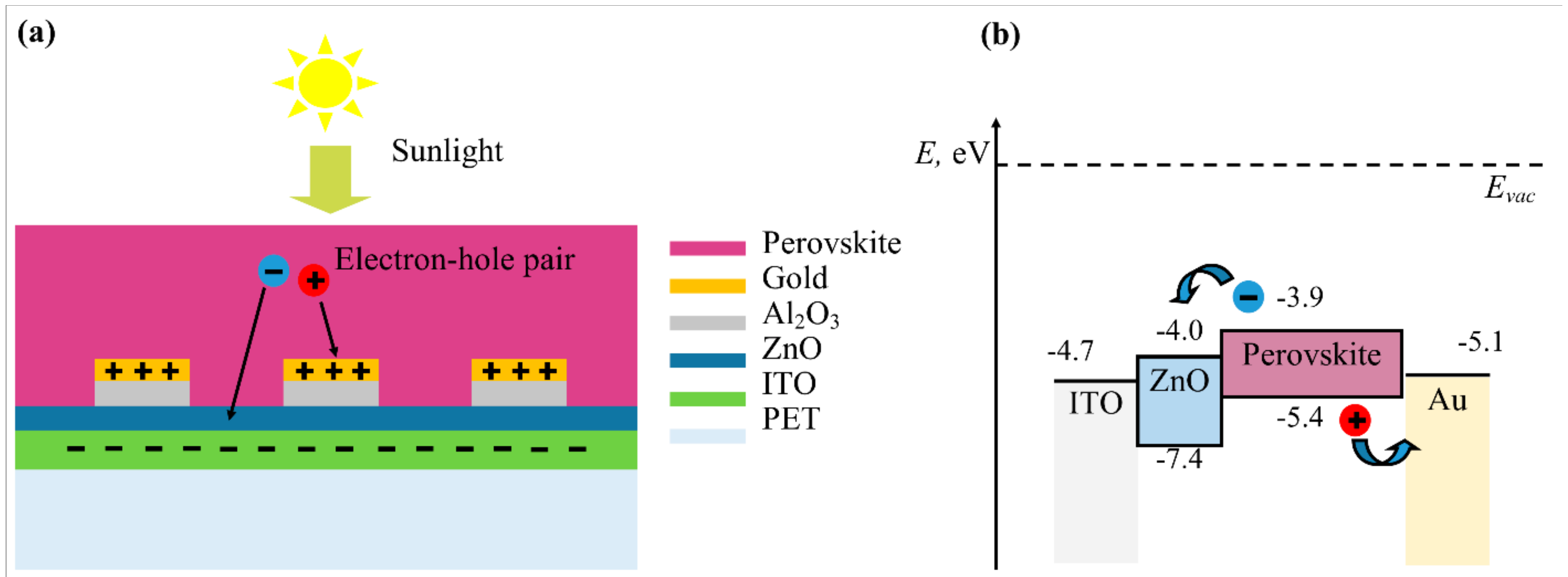
A sketch of the cross-section view of FQIBC PSCs is shown in Figure 2a. An approximate band alignment diagram for FQIBC PSCs is shown in Figure 2b. The work functions values of ITO and gold and the values for the energy of the conduction and valence band edges are taken from the literature [34,44,45].
2.3. Characterization
The cross-section images of the electrodes are obtained using a scanning electron microscope (Model: Crossbeam 540, Zeiss, Oberkochen, Germany). The optical images of the electrodes are obtained using an optical microscope (Model: Leica DM4000 B, Leica Microsystems, Wetzlar, Germany). The J-V curves of the FQIBC PSCs are measured using a solar simulator (Model: ORIEL Sol3A, Newport, Irvine, CA, USA) with AM1.5G solar irradiation at 100 mW/cm2 and a parameter analyzer (Model: B1500A, Keysight, Santa Rosa, CA, USA). The J-V curves of the devices are recorded with and without using neutral density optical filters (Model: NEK01S, Thorlabs, Newton, MA, USA). The spectral responses of the FQIBC PSCs are measured using an EQE measurement system (Model: ORIEL IQE 200, Newport, Irvine, CA, USA).
3. Results and Discussion
3.1. Experimental Part
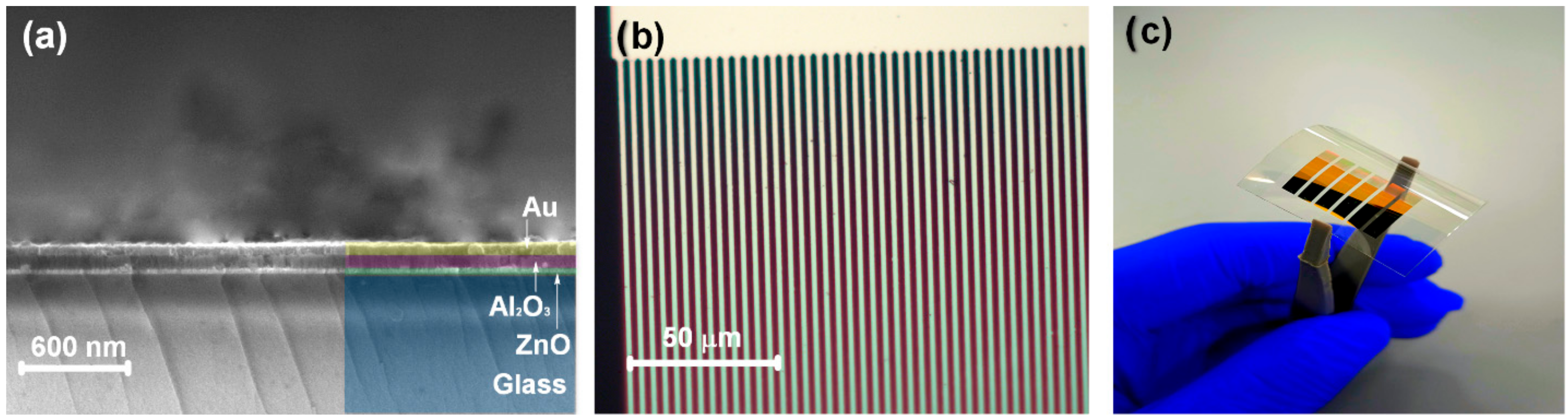
In order to evaluate the dimensions and structural quality of the back-contact electrodes, glass substrates are placed together with the PET substrates during the electrode functional layers (ZnO, Al2O3, and gold) deposition stages. Then, the cross-sections of these glass substrates with the deposited layers are analyzed using SEM imaging. A cross-section SEM micrograph of a sample shown in Figure 3a indicates that the electrode functional layers are homogeneous and conformal. An optical micrograph (see Figure 3b) of a prepared flexible back-contact electrode indicates that the electrodes are defect-free and have the desired structure. Figure 3c shows a photographic image of a prepared flexible back-contact electrode without the perovskite layer.
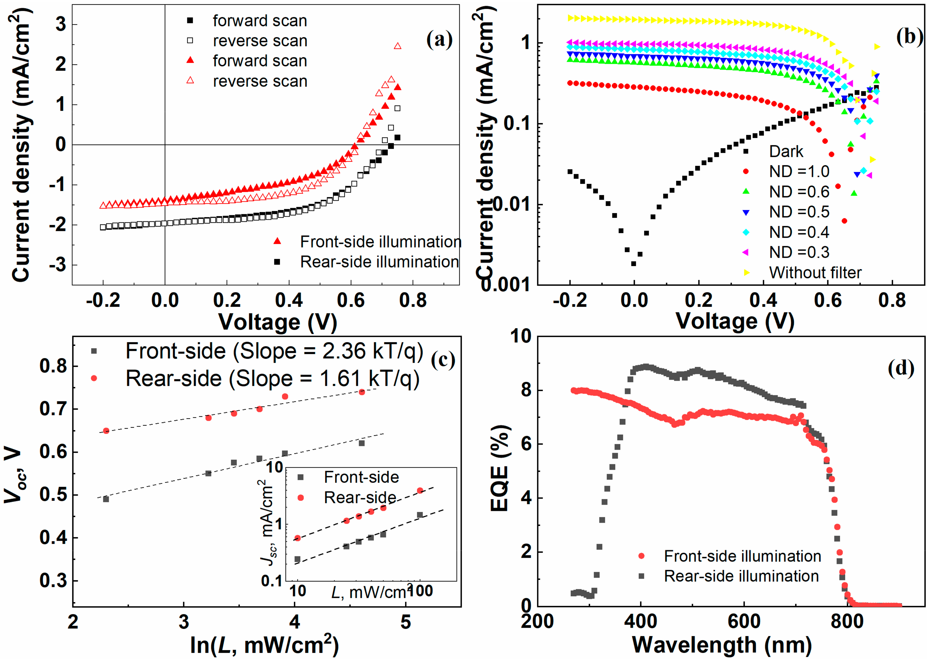
Current–voltage characteristics of the obtained FQIBC PSCs (shown in Figure 4a) are measured under AM1.5G irradiation. The measurements are performed for both front- (perovskite-side) and rear-side (PET-side) illumination options. The obtained FQIBC PSCs exhibit a small hysteresis effect as the J-V curves for the forward and reverse scans more or less coincide with each other (see Figure 4a). The photovoltaic parameters of the FQIBC PSC extracted from the J-V curves under illumination are displayed in Table 1. We note that the effective device area (0.04 cm2) is taken to be the same for both illumination options.
Comparison of the photovoltaic parameters for the front- and rear-side illumination indicate that except for the fill factor (), the short-circuit current (), the open-circuit voltage (), and the of the device under testing are slightly lower for the front-side illumination. This is a rather surprising result as it is expected that the photovoltaic parameters for the front-side illumination should be higher than the ones for the rear-side illumination. Indeed, the performance of FQIBC PSCs illuminated from the rear side should be lower due to light transmission losses and the shadowing effect of the metallic contacts of the anode layer (Al2O3/gold). However, the experimental results show the contrary. It is possible that this effect can be associated with the surface recombination of the photogenerated charge carriers. The surface of the typical solution-processed perovskite films is not ideal, and there are various macroscopic and microscopic defects and dangling chemical bonds on the surface of the perovskite films [46]. If the perovskite surface is exposed to the ambient air, as in the case of the current work, this can lead to further degradation of the perovskite layer surface quality due to chemical or/and physical adsorption of various atoms and molecules present in the environment. All this leads to appearance of the localized surface states on the perovskite surface, which can act as the recombination sites for charge carriers [47,48].
The dependence of J-V characteristics on light intensity is an effective and simple method for analyzing the dominant recombination mechanisms in PSCs [47,49]. The measurements of the J-V curves under different light intensities are also carried out when the devices are illuminated from the rear and the front side. Here, the measurements are performed under AM1.5G irradiation using neutral density filters with different optical densities. Figure 4b shows the J-V curves of a FQIBC PSC measured under different light intensities for the rear-side illumination. The J-V curves measured under different light intensities for the front-side illumination are shown in Supplementary Materials Figure S1. The dependence of the of the FQIBC PSC on the light intensity is linear for both illumination options (inset graph in Figure 4c). This indicates small charge carrier recombination losses under the short circuit conditions [50]. A relationship that describes the dependence of the open-circuit voltage on light intensity is given by the following equation [47,51]:
Here, is the Boltzmann’s constant, is the light ideality factor, is the absolute temperature, is the photocurrent, is the unit charge, and is the dark saturation current. Since the photocurrent is much higher than the dark saturation current and linearly depends on the light intensity, Equation (1) can be rewritten as the following:
where is the light intensity. Thus, it is possible to determine the light ideality factor from the slope of the dependence of on . The value of is obtained from the dependence of of the FQIBC PSC on the light intensity (see Figure 4c) is 1.61, which indicates the presence of trap-assisted Shockley–Reed–Hall (SRH) recombination pathway in the device [50,51,52]. A high value of (values close to 2) indicates recombination via deeper traps [52]. When the FQIBC PSC is illuminated from the front side, the value of becomes more than 2. This indicates a greater influence of traps on carrier recombination, which causes lower efficiency values. The physical origin of the traps can be caused by the polycrystalline nature of the perovskite film and the presence of defects at the grain boundaries [46]. In addition, since flexible substrates are used for the manufacturing of FQIBC PSCs, mechanical bending of the substrates is inevitable during the perovskite layer deposition and the device characterization steps. This leads to the formation of microcracks and deterioration of the structural integrity of devices.
Figure 4d shows the EQE spectra of a FQIBC PSC obtained for both illumination options. The EQE spectrum of the device under testing for the rear-side illumination exhibits an abrupt decrease below ~370 nm. The EQE spectrum of the device under test for the front-side illumination, on the other hand, remains high and even increases slowly as the wavelength of the incident light goes below ~370 nm. Such a disparity between the EQE spectra of the FQIBC PSC for different illumination options can be rationalized by the light transmission losses (absorption and reflection) occurring at the PET/ITO/ZnO layers when back-contact PSCs are illuminated from the rear side. This result nicely demonstrates the advantage of the back-contact configuration for solar cell device architecture in terms of reducing the light transmission losses and manufacturing PV and other optoelectronic devices (e.g., photodetectors) with wider spectral responses. A slightly lower EQE value for the front-side illumination is consistent with the J-V characteristics shown in Figure 4a.
3.2. Theoretical Part
To elucidate the underlying physical reason for the higher photovoltaic performance of the obtained FQIBC PSCs for the rear-side illumination and also to test our proposition on high values of the surface recombination rates in the devices, we examined the effect of the surface recombination rate on the performance of FQIBC PSCs using numerical simulation methods [53,54]. We used the standard drift-diffusion model [35,55] to calculate various electrical parameters of devices. For this, a set of equations of the standard drift-diffusion model is solved for the steady-state conditions (i.e., and ) using the COMSOL Multiphysics software for the presented device architecture. More details about the standard drift-diffusion model and the physical parameters of the materials used in the simulation experiments are given in Supplementary Materials Table S1.
A sketch of the cross-section of FQIBC PSCs used in the simulation experiments is shown in Supplementary Materials Figure S2. First, the simulation experiments are performed for the ideal case, in which the parameters of the device functional layers are the most optimum (see Supplementary Materials Table S1). The simulated J-V curves for the front- and rear-side illumination options and the most optimum device parameters are shown in Figure S3. The calculated maximum theoretical for the idealized device are 7.6% and 6.1% for the front- and rear-side illumination options, respectively.
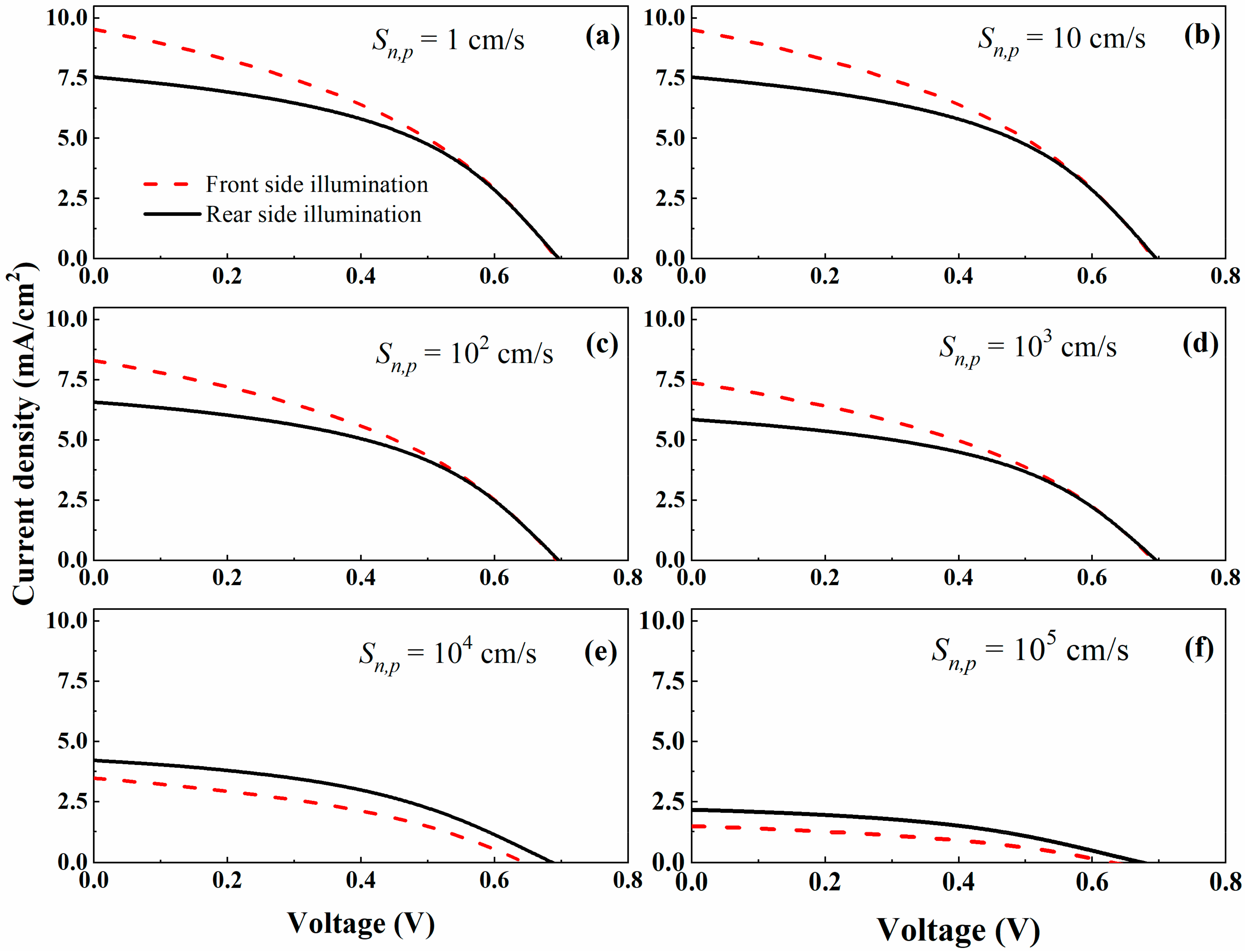
Next, we adjusted the input parameters for the simulation experiments to approach the real experimental values (see Supplementary Materials Table S1) and simulated the J-V curves for FQIBC PSCs by varying the surface recombination velocity for electrons and holes () from 1 cm/s to 105 cm/s. As shown in Figure 5a, the J-V curves of FQIBC PSCs exhibit a somewhat moderate behavior when the material parameters of the device functional layer are adjusted to approach the real experimental values and the shunt and sheet resistance values obtained from the experiments are taken into account. The device currents and values for the front-side illumination are higher than the ones for the rear-side illumination. Here, the value is taken to be equal to 1 cm/s. Increasing the value to 10 cm/s does not seem to affect the J-V characteristics of devices, as shown in Figure 5b. However, starting from = 103 cm/s, the J-V curves of FQIBC PSCs start degrading, as depicted in Figure 5c,d. When the value becomes 104 cm/s, not only a further degradation of the J-V curves is observed (see Figure 5e), but the device currents and values for the front-side illumination become lower than the ones for the rear-side illumination. This is similar to the J-V curves of the experimentally obtained FQIBC PSCs. When the value is as high as 105 cm/s, the simulated J-V curves (see Figure 5f) most closely approach the experimental J-V curves shown in Figure 4a. The photovoltaic parameters of FQIBC PSC extracted from the J-V curves shown in Figure 5 are displayed in the Supplementary Materials, Table S2.
Contrasting the experimentally and numerically obtained results suggest that the factor that is responsible for higher values of the device currents and the for the rear-side illumination could indeed be the high surface recombination rates in the perovskite layer of obtained FQIBC PSCs. Reducing the surface recombination rates (lower values of ≤ 103 cm/s) in the perovskite layer of FQIBC PSCs promise to result in higher device currents and PCEs values for the front-side illumination. One way to achieve this is to optimize the perovskite layer deposition process to obtain the perovskite photo-absorber layers with an improved crystalline and electronic nature [35]. In this regard, different deposition methods such as anti-solvent crystallization, hot-casting, thermal evaporation, and many other exciting new methods can be tested to achieve a perovskite photo-absorber layer with desired properties. Additionally, various passivation methods [56,57] can be employed to suppress the perovskite surface trap states and also to protect the perovskite layer from the degradation effects of the environment. Once these tasks are fulfilled, FQIBC PSCs may have a significant application potential in the emerging new technologies such as wearable/portable electronics, IoT technologies, and beyond.
4. Conclusions
In summary, a fabrication method for functional, flexible back-contact PSCs with quasi-interdigitated electrodes manufactured on PET/ITO substrates is demonstrated. Investigation of the photovoltaic properties of the obtained FQIBC PSCs shows that the devices have a higher performance when illuminated from the rear side. The analysis of the dependence of the open-circuit voltage on the light intensity indicates that the dominant recombination pathway in the devices is the Shockley–Read–Hall recombination. The measurements of the EQE spectra of the devices demonstrate that FQIBC PSCs have wider spectral response when illuminated from the front side. The computer simulation experiments on studying the effect of the surface recombination rate on the J-V characteristics of FQIBC PSCs have been carried out to rationalize the experimentally obtained results. Contrasting the experimental results with the simulation results reveals that high surface recombination rates in the perovskite layer might be the cause for the higher device performance values for the rear-side illumination. The simulation results also demonstrate that high surface recombination rates may also be one of the main factors that is limiting the device performance of the obtained FQIBC PSCs. Although the photovoltaic performance of the devices shown in this work are rather moderate, the computer simulation experiments demonstrate that with further optimization and improvements in device fabrication processes, FQIBC PSCs with the desired performances can be obtained. The findings of this work can be used as an example and guideline for the design and fabrication of high-performance FQIBC PSCs.
Supplementary Materials
The following supporting information can be downloaded at: https://www.mdpi.com/article/10.3390/en15093056/s1, Figure S1: J-V curves of a FQIBC PSC for the front-side illumination and different light intensities; Figure S2: Sketch of the cross-section view (shown in xz-plane) of the sunlight fall on FQIBC PSCs from the front- (perovskite-side) (a) and the rear-side (PET-side) (b). The areas enclosed with dashed white rectangles indicate the base unit areas used in simulation experiments; Figure S3: Comparison of the simulated J-V curves of FQIBC PSC for the front-side (dash red line) and the rear-side (solid black line) illumination; Table S1: Physical parameters used for simulation experiments; Table S2: The calculated photovoltaic parameters of FQIBC PSCs under AM1.5G solar irradiation [58,59,60,61,62,63,64,65,66,67,68].
Author Contributions
Conceptualization A.N.J.; methodology, H.P.P. and E.O.S.; formal analysis, H.P.P. and E.O.S.; investigation, H.P.P., E.O.S. and Z.U.; writing—original draft preparation, H.P.P. and A.N.J.; writing—review and editing, A.N.J. and K.N.D.; supervision A.N.J. and K.N.D. All authors have read and agreed to the published version of the manuscript.
Funding
This work has received funding from the Nazarbayev University Faculty Development Competitive Research Grant (Grant Number: 110119FD4512), Nazarbayev University Collaborative Research Grant (Grant Number: 021220CRP1922), Young Scientist Grant from the Ministry of Education and Science of the Republic of Kazakhstan (Grant Number: AP08052412).
Institutional Review Board Statement
Not applicable.
Informed Consent Statement
Not applicable.
Data Availability Statement
The data that support the findings of this study are available from the corresponding author upon reasonable request.
Acknowledgments
E.O.S. acknowledges support from the Postdoctoral Fellowship provided by Al-Farabi Kazakh National University.
Conflicts of Interest
The authors declare no conflict of interest.
References
- Kabir, D.; Forhad, T.; Ghann, W.; Richards, B.; Rahman, M.M.; Uddin, M.N.; Rakib, M.R.J.; Shariare, M.H.; Chowdhury, F.I.; Rabbani, M.M.; et al. Dye-Sensitized Solar Cell with Plasmonic Gold Nanoparticles Modified Photoanode. Nano-Struct. Nano-Objects 2021, 26, 100698. [Google Scholar] [CrossRef]
- Da Rosa, A.V.; Ordonez, J.C. Fundamentals of Renewable Energy Processes; Academic Press: Cambridge, MA, USA, 2021; ISBN 978-0-12-816037-4. [Google Scholar]
- Battaglia, C.; Cuevas, A.; Wolf, S.D. High-Efficiency Crystalline Silicon Solar Cells: Status and Perspectives. Energy Environ. Sci. 2016, 9, 1552–1576. [Google Scholar] [CrossRef] [Green Version]
- Dréon, J.; Jeangros, Q.; Cattin, J.; Haschke, J.; Antognini, L.; Ballif, C.; Boccard, M. 23.5%-Efficient Silicon Heterojunction Silicon Solar Cell Using Molybdenum Oxide as Hole-Selective Contact. Nano Energy 2020, 70, 104495. [Google Scholar] [CrossRef]
- Vollbrecht, J.; Brus, V.V. Effects of Recombination Order on Open-Circuit Voltage Decay Measurements of Organic and Perovskite Solar Cells. Energies 2021, 14, 4800. [Google Scholar] [CrossRef]
- Jiang, J.; Yang, X.; Huang, Y.; Li, M.; Tao, Q.; Fei, M.; Cai, H.L.; Zhang, F.M.; Wu, X.S. Improvement in Solar Cell Efficiency Based on the MAPbI3 Films Extracted by a Mixed Anti-Solvent. Appl. Phys. Lett. 2020, 117, 203901. [Google Scholar] [CrossRef]
- Zhu, Y.; Shu, L.; Zhang, Q.; Zhu, Y.; Poddar, S.; Wang, C.; He, Z.; Fan, Z. Moth Eye-Inspired Highly Efficient, Robust, and Neutral-Colored Semitransparent Perovskite Solar Cells for Building-Integrated Photovoltaics. EcoMat 2021, 3, e12117. [Google Scholar] [CrossRef]
- Li, W.; Wang, H.; Hu, X.; Cai, W.; Zhang, C.; Wang, M.; Zang, Z. Sodium Benzenesulfonate Modified Poly (3,4-Ethylenedioxythiophene): Polystyrene Sulfonate with Improved Wettability and Work Function for Efficient and Stable Perovskite Solar Cells. Sol. RRL 2021, 5, 2000573. [Google Scholar] [CrossRef]
- Yan, J.; Saunders, B.R. Third-Generation Solar Cells: A Review and Comparison of Polymer:Fullerene, Hybrid Polymer and Perovskite Solar Cells. RSC Adv. 2014, 4, 43286–43314. [Google Scholar] [CrossRef]
- Kojima, A.; Teshima, K.; Shirai, Y.; Miyasaka, T. Organometal Halide Perovskites as Visible-Light Sensitizers for Photovoltaic Cells. J. Am. Chem. Soc. 2009, 131, 6050–6051. [Google Scholar] [CrossRef]
- Im, J.-H.; Lee, C.-R.; Lee, J.-W.; Park, S.-W.; Park, N.-G. 6.5% Efficient Perovskite Quantum-Dot-Sensitized Solar Cell. Nanoscale 2011, 3, 4088–4093. [Google Scholar] [CrossRef] [Green Version]
- Eperon, G.E.; Leijtens, T.; Bush, K.A.; Prasanna, R.; Green, T.; Wang, J.T.-W.; McMeekin, D.P.; Volonakis, G.; Milot, R.L.; May, R.; et al. Perovskite-Perovskite Tandem Photovoltaics with Optimized Band Gaps. Science 2016, 354, 861–865. [Google Scholar] [CrossRef] [PubMed] [Green Version]
- Hu, Z.; Lin, Z.; Su, J.; Zhang, J.; Chang, J.; Hao, Y. A Review on Energy Band-Gap Engineering for Perovskite Photovoltaics. Sol. RRL 2019, 3, 1900304. [Google Scholar] [CrossRef]
- Wehrenfennig, C.; Eperon, G.E.; Johnston, M.B.; Snaith, H.J.; Herz, L.M. High Charge Carrier Mobilities and Lifetimes in Organolead Trihalide Perovskites. Adv. Mater. 2014, 26, 1584–1589. [Google Scholar] [CrossRef] [PubMed] [Green Version]
- Zhu, X.; Su, H.; Marcus, R.A.; Michel-Beyerle, M.E. Computed and Experimental Absorption Spectra of the Perovskite CH3NH3PbI3. J. Phys. Chem. Lett. 2014, 5, 3061–3065. [Google Scholar] [CrossRef]
- Rolston, N.; Scheideler, W.J.; Flick, A.C.; Chen, J.P.; Elmaraghi, H.; Sleugh, A.; Zhao, O.; Woodhouse, M.; Dauskardt, R.H. Rapid Open-Air Fabrication of Perovskite Solar Modules. Joule 2020, 4, 2675–2692. [Google Scholar] [CrossRef]
- Tong, G.; Son, D.-Y.; Ono, L.K.; Kang, H.-B.; He, S.; Qiu, L.; Zhang, H.; Liu, Y.; Hieulle, J.; Qi, Y. Removal of Residual Compositions by Powder Engineering for High Efficiency Formamidinium-Based Perovskite Solar Cells with Operation Lifetime over 2000 h. Nano Energy 2021, 87, 106152. [Google Scholar] [CrossRef]
- Wu, T.; Qin, Z.; Wang, Y.; Wu, Y.; Chen, W.; Zhang, S.; Cai, M.; Dai, S.; Zhang, J.; Liu, J.; et al. The Main Progress of Perovskite Solar Cells in 2020–2021. Nano-Micro Lett. 2021, 13, 152. [Google Scholar] [CrossRef]
- Green, M.; Dunlop, E.; Hohl-Ebinger, J.; Yoshita, M.; Kopidakis, N.; Hao, X. Solar Cell Efficiency Tables (Version 57). Prog. Photovolt. Res. Appl. 2021, 29, 3–15. [Google Scholar] [CrossRef]
- Mishra, S.; Ghosh, S.; Singh, T. Progress in Materials Development for Flexible Perovskite Solar Cells and Future Prospects. ChemSusChem 2021, 14, 512–538. [Google Scholar] [CrossRef]
- Saianand, G.; Sonar, P.; Wilson, G.J.; Gopalan, A.-I.; Roy, V.A.L.; Unni, G.E.; Mamun Reza, K.; Bahrami, B.; Venkatramanan, K.; Qiao, Q. Current Advancements on Charge Selective Contact Interfacial Layers and Electrodes in Flexible Hybrid Perovskite Photovoltaics. J. Energy Chem. 2021, 54, 151–173. [Google Scholar] [CrossRef]
- Lan, Y.; Wang, Y.; Song, Y. Efficient Flexible Perovskite Solar Cells Based on a Polymer Additive. Flex. Print. Electron. 2020, 5, 014001. [Google Scholar] [CrossRef]
- Lee, S.; Shi, Q.; Lee, C. From Flexible Electronics Technology in the Era of IoT and Artificial Intelligence toward Future Implanted Body Sensor Networks. APL Mater. 2019, 7, 031302. [Google Scholar] [CrossRef] [Green Version]
- Kirtania, S.G.; Elger, A.W.; Hasan, M.R.; Wisniewska, A.; Sekhar, K.; Karacolak, T.; Sekhar, P.K. Flexible Antennas: A Review. Micromachines 2020, 11, 847. [Google Scholar] [CrossRef]
- Mujahid, M.; Chen, C.; Hu, W.; Wang, Z.-K.; Duan, Y. Progress of High-Throughput and Low-Cost Flexible Perovskite Solar Cells. Sol. RRL 2020, 4, 1900556. [Google Scholar] [CrossRef]
- Zhang, J.; Zhang, W.; Cheng, H.-M.; Silva, S.R.P. Critical Review of Recent Progress of Flexible Perovskite Solar Cells. Mater. Today 2020, 39, 66–88. [Google Scholar] [CrossRef]
- Zi, W.; Jin, Z.; Liu, S.; Xu, B. Flexible Perovskite Solar Cells Based on Green, Continuous Roll-to-Roll Printing Technology. J. Energy Chem. 2018, 27, 971–989. [Google Scholar] [CrossRef] [Green Version]
- Abate, A.; Correa-Baena, J.-P.; Saliba, M.; Su’ait, M.S.; Bella, F. Perovskite Solar Cells: From the Laboratory to the Assembly Line. Chem. Eur. J. 2018, 24, 3083–3100. [Google Scholar] [CrossRef]
- Yang, D.; Yang, R.; Priya, S.; Liu, S.F. Recent Advances in Flexible Perovskite Solar Cells: Fabrication and Applications. Angew. Chem. Int. Ed. 2019, 58, 4466–4483. [Google Scholar] [CrossRef]
- Xie, H.; Yin, X.; Guo, Y.; Liu, J.; Que, W.; Wang, G. Recent Progress of Flexible Perovskite Solar Cells. Phys. Status Solidi RRL 2019, 13, 1800566. [Google Scholar] [CrossRef]
- Zeng, P.; Deng, W.; Liu, M. Recent Advances of Device Components toward Efficient Flexible Perovskite Solar Cells. Sol. RRL 2020, 4, 1900485. [Google Scholar] [CrossRef]
- Yoon, J.; Sung, H.; Lee, G.; Cho, W.; Ahn, N.; Suk Jung, H.; Choi, M. Superflexible, High-Efficiency Perovskite Solar Cells Utilizing Graphene Electrodes: Towards Future Foldable Power Sources. Energy Environ. Sci. 2017, 10, 337–345. [Google Scholar] [CrossRef]
- Yang, L.; Xiong, Q.; Li, Y.; Gao, P.; Xu, B.; Lin, H.; Li, X.; Miyasaka, T. Artemisinin-Passivated Mixed-Cation Perovskite Films for Durable Flexible Perovskite Solar Cells with over 21% Efficiency. J. Mater. Chem. 2021, 9, 1574–1582. [Google Scholar] [CrossRef]
- Jumabekov, A.N.; Gaspera, E.D.; Xu, Z.-Q.; Chesman, A.S.R.; van Embden, J.; Bonke, S.A.; Bao, Q.; Vak, D.; Bach, U. Back-Contacted Hybrid Organic–Inorganic Perovskite Solar Cells. J. Mater. Chem. C 2016, 4, 3125–3130. [Google Scholar] [CrossRef]
- Yang, Z.; Yang, W.; Yang, X.; Greer, J.C.; Sheng, J.; Yan, B.; Ye, J. Device Physics of Back-Contact Perovskite Solar Cells. Energy Environ. Sci. 2020, 13, 1753–1765. [Google Scholar] [CrossRef]
- Yang, W.; Yang, Z.; Shou, C.; Sheng, J.; Yan, B.; Ye, J. Optical Design and Optimization for Back-Contact Perovskite Solar Cells. Sol. Energy 2020, 201, 84–91. [Google Scholar] [CrossRef]
- Prince, K.J.; Nardone, M.; Dunfield, S.P.; Teeter, G.; Mirzokarimov, M.; Warren, E.L.; Moore, D.T.; Berry, J.J.; Wolden, C.A.; Wheeler, L.M. Complementary Interface Formation toward High-Efficiency All-Back-Contact Perovskite Solar Cells. Cell Rep. 2021, 2, 100363. [Google Scholar] [CrossRef]
- Lin, X.; Lu, J.; Raga, S.R.; McMeekin, D.P.; Ou, Q.; Scully, A.D.; Tan, B.; Chesman, A.S.R.; Deng, S.; Zhao, B.; et al. Balancing Charge Extraction for Efficient Back-Contact Perovskite Solar Cells by Using an Embedded Mesoscopic Architecture. Adv. Energy Mater. 2021, 11, 2100053. [Google Scholar] [CrossRef]
- Lin, X.; Chesman, A.S.R.; Raga, S.R.; Scully, A.D.; Jiang, L.; Tan, B.; Lu, J.; Cheng, Y.-B.; Bach, U. Effect of Grain Cluster Size on Back-Contact Perovskite Solar Cells. Adv. Funct. Mater. 2018, 28, 1805098. [Google Scholar] [CrossRef]
- Wong-Stringer, M.; Routledge, T.J.; McArdle, T.; Wood, C.J.; Game, O.S.; Smith, J.A.; Bishop, J.E.; Vaenas, N.; Coles, D.M.; Buckley, A.R.; et al. A Flexible Back-Contact Perovskite Solar Micro-Module. Energy Environ. Sci. 2019, 12, 1928–1937. [Google Scholar] [CrossRef] [Green Version]
- Xiao, M.; Huang, F.; Huang, W.; Dkhissi, Y.; Zhu, Y.; Etheridge, J.; Gray-Weale, A.; Bach, U.; Cheng, Y.-B.; Spiccia, L. A Fast Deposition-Crystallization Procedure for Highly Efficient Lead Iodide Perovskite Thin-Film Solar Cells. Angew. Chem. Int. Ed. 2014, 53, 9898–9903. [Google Scholar] [CrossRef]
- Huang, F.; Dkhissi, Y.; Huang, W.; Xiao, M.; Benesperi, I.; Rubanov, S.; Zhu, Y.; Lin, X.; Jiang, L.; Zhou, Y.; et al. Gas-Assisted Preparation of Lead Iodide Perovskite Films Consisting of a Monolayer of Single Crystalline Grains for High Efficiency Planar Solar Cells. Nano Energy 2014, 10, 10–18. [Google Scholar] [CrossRef]
- Conings, B.; Babayigit, A.; Klug, M.T.; Bai, S.; Gauquelin, N.; Sakai, N.; Wang, J.T.-W.; Verbeeck, J.; Boyen, H.-G.; Snaith, H.J. A Universal Deposition Protocol for Planar Heterojunction Solar Cells with High Efficiency Based on Hybrid Lead Halide Perovskite Families. Adv. Mater. 2016, 28, 10701–10709. [Google Scholar] [CrossRef] [PubMed]
- Kumawat, N.K.; Gupta, D.; Kabra, D. Recent Advances in Metal Halide-Based Perovskite Light-Emitting Diodes. Energy Technol. 2017, 5, 1734–1749. [Google Scholar] [CrossRef] [Green Version]
- Adjokatse, S.; Fang, H.-H.; Loi, M.A. Broadly Tunable Metal Halide Perovskites for Solid-State Light-Emission Applications. Mater. Today 2017, 20, 413–424. [Google Scholar] [CrossRef]
- Park, N.G.; Miyasaka, T.; Grätzel, M. Organic-Inorganic Halide Perovskite Photovoltaics; Springer: Cham, Switzerland, 2016; ISBN 978-3-319-35112-4. [Google Scholar]
- Fahrenbruch, A.; Bube, R. Fundamentals of Solar Cells: Photovoltaic Solar Energy Conversion; Elsevier: Amsterdam, The Netherlands, 2012; ISBN 978-0-323-14538-1. [Google Scholar]
- Shalimova, K.V. Physics of Semiconductors; Lan: Moscow, Russia, 2010; ISBN 978-5-8114-0922-8. [Google Scholar]
- Kumar, P.; Jain, S.C.; Kumar, H.; Chand, S.; Kumar, V. Effect of Illumination Intensity and Temperature on Open Circuit Voltage in Organic Solar Cells. Appl. Phys. Lett. 2009, 94, 183505. [Google Scholar] [CrossRef] [Green Version]
- Brus, V.V.; Proctor, C.M.; Ran, N.A.; Nguyen, T.-Q. Capacitance Spectroscopy for Quantifying Recombination Losses in Nonfullerene Small-Molecule Bulk Heterojunction Solar Cells. Adv. Energy Mater. 2016, 6, 1502250. [Google Scholar] [CrossRef]
- Kirchartz, T.; Deledalle, F.; Tuladhar, P.S.; Durrant, J.R.; Nelson, J. On the Differences between Dark and Light Ideality Factor in Polymer:Fullerene Solar Cells. J. Phys. Chem. Lett. 2013, 4, 2371–2376. [Google Scholar] [CrossRef]
- Kirchartz, T.; Nelson, J. Meaning of Reaction Orders in Polymer: Fullerene Solar Cells. Phys. Rev. B 2012, 86, 165201. [Google Scholar] [CrossRef] [Green Version]
- Shalenov, E.O.; Dzhumagulova, K.N.; Ng, A.; Jumabekov, A.N. Performance Optimization of Back-Contact Perovskite Solar Cells with Quasi-Interdigitated Electrodes. Sol. Energy 2020, 205, 102–108. [Google Scholar] [CrossRef]
- Shalenov, E.O.; Dzhumagulova, K.N.; Seitkozhanov, Y.S.; Ng, A.; Valagiannopoulos, C.; Jumabekov, A.N. Insights on Desired Fabrication Factors from Modeling Sandwich and Quasi-Interdigitated Back-Contact Perovskite Solar Cells. ACS Appl. Energy Mater. 2021, 4, 1093–1107. [Google Scholar] [CrossRef]
- Lopez-Varo, P.; Jiménez-Tejada, J.A.; García-Rosell, M.; Ravishankar, S.; Garcia-Belmonte, G.; Bisquert, J.; Almora, O. Device Physics of Hybrid Perovskite Solar Cells: Theory and Experiment. Adv. Energy Mater. 2018, 8, 1702772. [Google Scholar] [CrossRef]
- Wang, S.; Wu, T.; Qiu, J.; Wang, R.; Zhu, Z.; Zhang, X.; Hua, Y. Enhanced Electron Transfer Dynamics in Perylene Diimide Passivated Efficient and Stable Perovskite Solar Cells. EcoMat 2021, 3, e12146. [Google Scholar] [CrossRef]
- Azam, M.; Khan, A.A.; Liang, G.-X.; Li, G.-J.; Chen, S.; Zheng, Z.-H.; Farooq, U.; Ishaq, M.; Fan, P.; Wang, Z.; et al. Examining the Interfacial Defect Passivation with Chlorinated Organic Salt for Highly Efficient and Stable Perovskite Solar Cells. Sol. RRL 2020, 4, 2000358. [Google Scholar] [CrossRef]
- Sze, S.M.; Ng, K.K. Physics of Semiconductor Devices, 3rd ed.; John Wiley & Sons: Hoboken, NJ, USA, 2007; pp. 79–124. [Google Scholar]
- Hall, R.N. Electron-Hole Recombination in Germanium. Phys. Rev. 1952, 87, 387. [Google Scholar] [CrossRef]
- Shockley, W.; Read, W.T., Jr. Statistics of the Recombinations of Holes and Electrons. Phys. Rev. 1952, 87, 62–69. [Google Scholar] [CrossRef]
- Azri, F.; Meftah, A.; Sengouga, N.; Meftah, A. Electron and hole transport layers optimization by numerical simulation of a perovskite solar cell. Sol. Energy 2019, 181, 372–378. [Google Scholar] [CrossRef]
- Hu, Y.; Adhyaksa, G.W.P.; DeLuca, G.; Simonov, A.N.; Duffy, N.W.; Reichmanis, E.; Bach, U.; Docampo, P.; Bein, T.; Garnett, E.C.; et al. Perovskite solar cells with a hybrid electrode structure. AIP Adv. 2019, 9, 125037. [Google Scholar] [CrossRef] [Green Version]
- Casas, G.; Cappelletti, M.; Cedola, A.; Soucase, B.M.; Blancá, E.P.Y. Analysis of the power conversion efficiency of perovskite solar cells with different materials as Hole-Transport Layer by numerical simulations. Superlattices Microstruct. 2017, 107, 136–143. [Google Scholar] [CrossRef]
- Kiermasch, D.; Rieder, P.; Tvingstedt, K.; Baumann, A.; Dyakonov, V. Improved charge carrier lifetime in planar perovskite solar cells by bromine doping. Sci. Rep. 2016, 6, 39333. [Google Scholar] [CrossRef]
- Maynard, B.; Long, Q.; Schiff, E.A.; Yang, M.; Zhu, K.; Kottokkaran, R.; Abbas, H.; Dalal, V.L. Electron and hole drift mobility measurements on methylammonium lead iodide perovskite solar cells. Appl. Phys. Lett. 2016, 108, 173505. [Google Scholar] [CrossRef]
- Kirchartz, T.; Krückemeier, L.; Unger, E.L. Research Update: Recombination and open-circuit voltage in lead-halide perovskites. APL Mater. 2018, 6, 100702. [Google Scholar] [CrossRef] [Green Version]
- Idígoras, J.; Contreras-Bernal, L.; Cave, J.M.; Courtier, N.; Barranco, Á.; Borras, A.; Sánchez-Valencia, J.R.; Anta, J.A.; Walker, A.B. The Role of Surface Recombination on the Performance of Perovskite Solar Cells: Effect of Morphology and Crystalline Phase of TiO2 Contact. Adv. Mater. Interfaces 2018, 5, 1801076. [Google Scholar] [CrossRef]
- Li, Y.; Yan, W.; Li, Y.; Wang, S.; Wang, W.; Bian, Z.; Xiao, L.; Gong, Q. Direct Observation of Long Electron-Hole Diffusion Distance in CH3NH3PbI3 Perovskite Thin Film. Sci. Rep. 2015, 5, 14485. [Google Scholar] [CrossRef] [PubMed]
Figure 1.
Flowchart depicting the FQIBC PSC fabrication process and schematic diagram of the final device.
Figure 1.
Flowchart depicting the FQIBC PSC fabrication process and schematic diagram of the final device.

Figure 2.
(a) Schematic representation of the FQIBC PSC operation principle. (b) Approximate band diagram for FQIBC PSCs.
Figure 2.
(a) Schematic representation of the FQIBC PSC operation principle. (b) Approximate band diagram for FQIBC PSCs.

Figure 3.
(a) SEM image of a glass substrate with the ZnO, Al2O3, and gold layers (device functional layers); (b) optical microscope image of a flexible back-contact electrode (magnification: ×50); (c) photographic image of a flexible back-contact electrode.
Figure 3.
(a) SEM image of a glass substrate with the ZnO, Al2O3, and gold layers (device functional layers); (b) optical microscope image of a flexible back-contact electrode (magnification: ×50); (c) photographic image of a flexible back-contact electrode.

Figure 4.
(a) J-V curves of a FQIBC PSC measured under AM1.5G solar irradiation at 100 mW/cm2. The measurements are performed for the front- and rear-side illumination options. (b) J-V curves of the FQIBC PSC under different light intensity. (c) The dependence of open-circuit voltage on light intensity. The inset graph shows the dependence of the short-circuit current on the light intensity. (d) EQE spectra of the FQIBC PSC measured for the front- and rear-side illumination options.

Figure 5.
J-V curves of FQIBC PSCs for different values of the electron/hole surface recombination velocity (). The dashed red lines are for the front-side illumination, whereas the solid black lines are for the rear-side illumination of devices. J-V curves of FQIBC PSCs when = 1 cm/s (a), = 10 cm/s (b), = 102 cm/s (c), = 103 cm/s (d), = 104 cm/s (e), and = 105 cm/s (f).


Table 1.
The photovoltaic parameters of a FQIBC PSCs under AM1.5G solar irradiation.
| Illumination | , V | , mA/cm2 | , % | |
|---|---|---|---|---|
| Front-side | 0.62 | 1.4 | 0.55 | 0.5 |
| Rear-side | 0.7 | 1.96 | 0.54 | 0.74 |
Publisher’s Note: MDPI stays neutral with regard to jurisdictional claims in published maps and institutional affiliations. |
© 2022 by the authors. Licensee MDPI, Basel, Switzerland. This article is an open access article distributed under the terms and conditions of the Creative Commons Attribution (CC BY) license (https://creativecommons.org/licenses/by/4.0/).
Share and Cite
MDPI and ACS Style
Parkhomenko, H.P.; Shalenov, E.O.; Umatova, Z.; Dzhumagulova, K.N.; Jumabekov, A.N. Fabrication of Flexible Quasi-Interdigitated Back-Contact Perovskite Solar Cells. Energies 2022, 15, 3056. https://doi.org/10.3390/en15093056
AMA Style
Parkhomenko HP, Shalenov EO, Umatova Z, Dzhumagulova KN, Jumabekov AN. Fabrication of Flexible Quasi-Interdigitated Back-Contact Perovskite Solar Cells. Energies. 2022; 15(9):3056. https://doi.org/10.3390/en15093056
Chicago/Turabian StyleParkhomenko, Hryhorii P., Erik O. Shalenov, Zarina Umatova, Karlygash N. Dzhumagulova, and Askhat N. Jumabekov. 2022. "Fabrication of Flexible Quasi-Interdigitated Back-Contact Perovskite Solar Cells" Energies 15, no. 9: 3056. https://doi.org/10.3390/en15093056
Note that from the first issue of 2016, this journal uses article numbers instead of page numbers. See further details here.