Single JFET Front-End Amplifier for Low Frequency Noise Measurements with Cross Correlation-Based Gain Calibration


Department of Engineering, University of Messina, 98166 Messina, Italy
*
Author to whom correspondence should be addressed.
Electronics 2019, 8(10), 1197; https://doi.org/10.3390/electronics8101197
Submission received: 10 September 2019
/
Revised: 7 October 2019
/
Accepted: 18 October 2019
/
Published: 21 October 2019
(This article belongs to the Special Issue Advances in Low-Frequency Noise Measurements)
Abstract
:We propose an open loop voltage amplifier topology based on a single JFET front-end for the realization of very low noise voltage amplifiers to be used in the field of low frequency noise measurements. With respect to amplifiers based on differential input stages, a single transistor stage has, among others, the advantage of a lower background noise. Unfortunately, an open loop approach, while simplifying the realization, has the disadvantage that because of the dispersions in the characteristics of the active device, it cannot ensure that a well-defined gain be obtained by design. To address this issue, we propose to add two simple operational amplifier-based auxiliary amplifiers with known gain as part of the measurement chain and employ cross correlation for the calibration of the gain of the main amplifier. With proper data elaboration, gain calibration and actual measurements can be carried out at the same time. By using the approach we propose, we have been able to design a low noise amplifier relying on a simplified hardware and with background noise as low as 6 nV/√Hz at 200 mHz, 1.7 nV/√Hz at 1 Hz, 0.7 nV/√Hz at 10 Hz, and less than 0.6 nV/√Hz at frequencies above 100 Hz.
1. Introduction
Low frequency noise measurements (LFNMs) are among the most sensitive tools for the investigation of the quality and reliability of electron devices and systems [1]. While LFNMs are especially useful in the investigation of the quality and reliability of electron devices [2,3,4,5,6] and in the investigation of the conduction mechanisms of advanced electron devices [7,8,9], the application of LFNMs in the development of advanced sensing approaches has been suggested [10,11,12]. Performing meaningful noise measurements, however, requires that the background noise (BN) of the measurement chain be much smaller than the noise to be detected. This is especially true in the case of low frequencies (f < 1Hz) where the low frequency noise introduced by the instrumentation usually sets the lower limit of the background noise that can be obtained. It is worth noting that cross correlation approaches that allow reaching a BN level well below that of the amplifier employed in the measurement are barely effective at very low frequencies because of the very long measurement time that would be required for averaging out the uncorrelated noise sources [13,14,15]. It is for this reason that it is important to design noise preamplifiers with the lowest possible level of BN at very low frequencies. In the case of voltage noise measurements, the BN of the system can be reduced to the equivalent input voltage noise (EIVN) of the voltage amplifier directly connected to the device under test (DUT). A possible approach to the design of very low noise voltage amplifiers is to add a differential stage based on discrete, very low noise devices in front of a solid-state high-gain stage. In this way, the entire system can be regarded as a very low noise operational amplifier (OA) whose gain can be set and stabilized by means of passive feedback [16,17,18,19]. This approach has the added advantage that because of the differential input stage, coupling to the DUT down to DC is possible, which can be relevant in the field of LFNMs, where the frequencies of interest may extend well below 1 Hz [20]. While the lowest level of EIVN are obtained by employing BJT based input stages, JFET input stages are preferred in all those cases in which noise is to be measured on nodes where a significant DC component is present. This is often the case in the field of noise measurements on electron devices, since measurements need to be performed on biased DUTs. Using BJTs, AC coupling down to the tens of mHz range would be made quite difficult because of the large bias currents and equivalent input noise current of these devices [20].
When compared to a common source (CS), open loop, single transistor stage, however, the EIVN of a low noise amplifier employing a differential JFET input stage is at least doubled because both transistors in the input stage equally contribute to the BN [18]. Moreover, obtaining stability when dealing with an operational amplifier based on a discrete component input stage is never an easy task, and frequency compensation often results in reduced bandwidth and BN increase at higher frequencies [18,19]. On the other hand, the voltage gain of an open loop CS stage directly depends on the characteristics of the active device so that known and stable gain cannot be guaranteed by design. This means that calibration measurements with known noise sources must be performed in order to obtain the actual gain of the amplifier, or gain adjustment circuitry needs to be added in order to set the gain to the desired value. In order to address these issues, we propose, in this paper, an approach that aims to take full advantage of the noise performances and simplicity of design of an open loop low noise amplifier based on a CS JFET stage while avoiding, at the same time, the need for time-consuming measurements for gain calibration and/or gain adjustment. As it will be shown in the following, by resorting to auxiliary OA based amplifiers operating in parallel with the main CS JFET low noise amplifier, the value of the gain of the main amplifier can be obtained by cross correlation while noise measurements on the device or system under investigation are in progress.
2. Proposed Approach
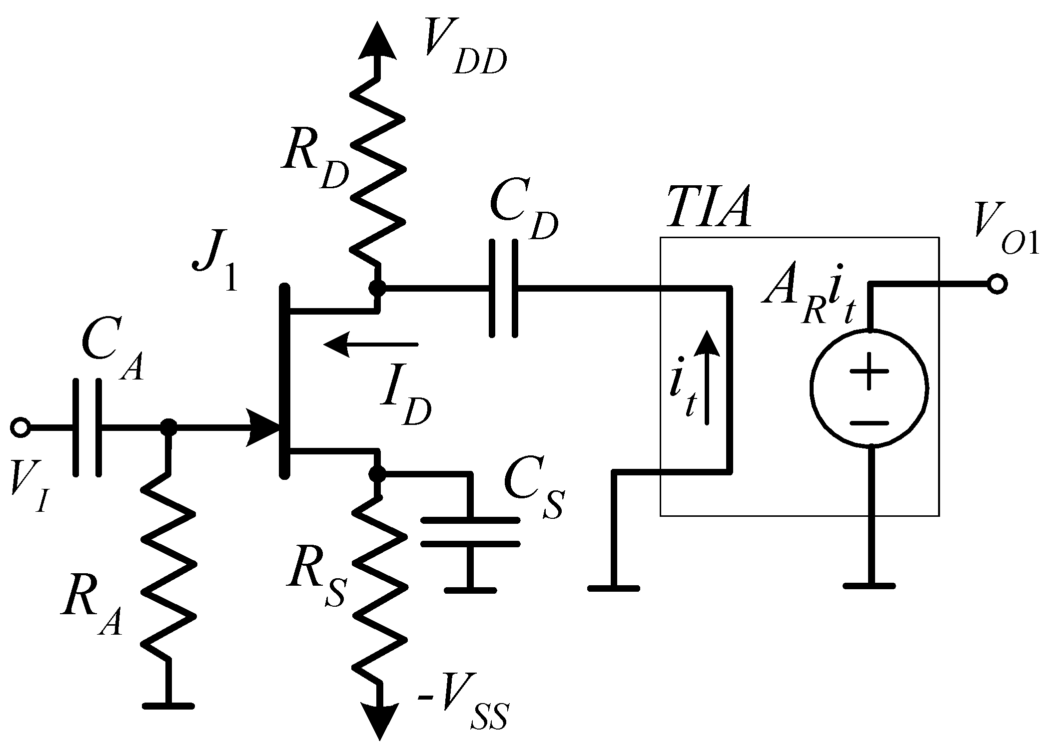
We start by analyzing the properties of the circuit in Figure 1 that can be regarded as the cascade of a JFET CS amplifier followed by an ideal transimpedance amplifier (TIA) stage with gain AR. In the actual circuit, the TIA is implemented with an OA in shunt-shunt feedback configuration [21]. The (ideal) circuit in Figure 1 can be regarded as a good representation of the actual circuit as long as the input impedance of the TIA is much smaller than the impedance of the capacitor CD at all frequencies of interest. We assume a dual supply operation (that is required, in any case, for a simple implementation of the TIA). In our design we employ an IF3601 large area JFET by InterFet, capable of providing transconductance gains (gm) in the order of a few tens of mA/V with a bias drain current in the order of a few mA [18]. This device is characterized by an equivalent input noise that can be as low as 0.3 nV/√Hz at 100 Hz. As is characteristic of JFET devices, DC and AC parameters are quite spread. The datasheet for IF3601 lists a pinch off voltage in the interval from −2 up to −0.35 V, while only a minimum value for the saturation current at VGS = 0 is given. Assuming that the JFET is in the active region of operation and that the gate current is negligible, in the circuit configuration in Figure 1, we have
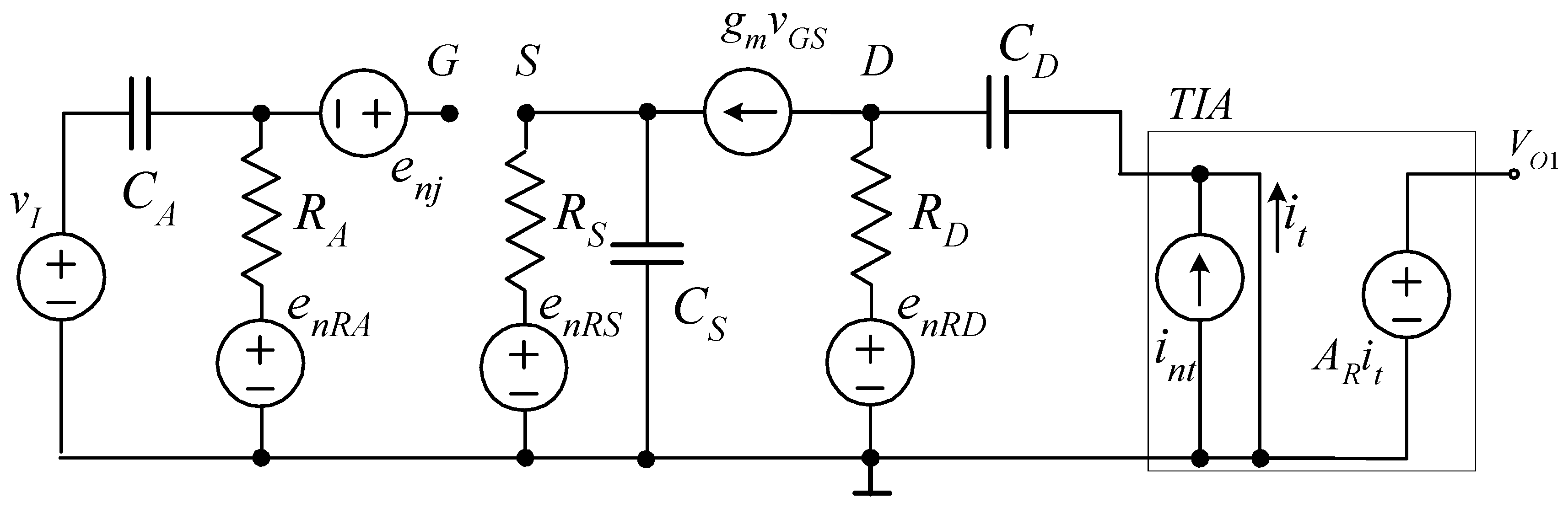
While the actual value of ID depends on the characteristic of the particular JFET used in the circuit, the fact that −VGS is certainly smaller than 2 V (typically in the order of a few hundred mV for currents in the order of a few mA) means that for VSS equal to 6 V or more, the bias current (ID) can be set with a reasonable error (typically less than 10%) by the ratio VSS/RS. In other words, with the simple bias configuration in Figure 1, the effect of parameter dispersion is modest, as far as the bias point is concerned. Note, however, that this does not imply in any way that we can ensure, by design, a predictable and known gain for the amplifier, since even for the same bias current, the transconductance gain can change significantly depending on the particular device being used. When employing the amplifier in Figure 1 as part of a noise measurement system, the knowledge of the actual gain is, of course, necessary. In principle, one could perform calibration measurements once each single amplifier is built or change some circuit parameter until the desired gain is obtained [22]. However, since the gain can change with the temperature and also because of ageing of the components, the only way to ensure accuracy in actual measurements is to frequently repeat the calibration procedure. Before discussing the approach we propose for addressing this issue, we need to devote our attention to the frequency response that can be obtained from the amplifier in Figure 1. Indeed, since we are interested in an amplifier to be used in LFNM applications, we need to extend the lower frequency limit well below 1 Hz. The small signal input–output transfer function of the circuit in Figure 1 can be calculated starting from the small signal equivalent circuit in Figure 2, where all the relevant noise sources are also included. As far as the transfer function is concerned, we can assume all noise sources inactive and we obtain:
where
From Equation (2), it is apparent that since (τ′s < τs), a constant frequency response is obtained for frequencies above the one corresponding to the pole with the largest magnitude. As far as the pole corresponding to τA is concerned, since the resistance RA can be in the order of a few MΩ, its frequency can be easily set below a few tens of mHz by employing for CA capacitances in the tens of μF range. In the case of the pole frequencies corresponding to τD and, especially, τ′s, the situation is quite different. With reference to Figure 1 and Equation (1), RS must be in the order of 1 kΩ in order to obtain bias currents in the order of a few mA. As a consequence, RD must also be in the same order of magnitude (with RD conveniently lower that RS in order to ensure that the JFET operates in the active region). When JFETs such as the one employed in our design are biased with a drain current in the order of a few mA, the transconductance gain gm is typically in the order of a few tens of mA/V. This means that the equivalent resistance RS′ (the resistance seen toward the source of the JFET) may be as low as a few tens of ohms. In this situation, the only way to obtain a value of τ′S in the order of a few seconds or tens of seconds (to obtain a pole frequency well below 1 Hz) is to resort to a capacitor value in the order of 1 F or more for CS (few tens of mF in the case of CD for obtaining τD >> 10 s).
While up to a few years ago, employing capacitances in the order of 1 F would have been largely impractical, supercapacitors in very compact size are nowadays easily available with capacitances ranging from a few mF to a few F. Unlike other high specific capacitance devices (electrolytic capacitors), supercapacitors have been shown to be compatible with instrumentation intended for LFNM applications [23,24,25]. Note that because of the circuit configuration in Figure 1, the DC voltage drop across the capacitor CS is −VGS that, in the case of the JFET we employ in our design, is typically below 1 V, and this allows for employing supercapacitors in the order of a few farads with a bias voltage well below the maximum rated value. As far as the BN is concerned, for the sake of simplicity, we will limit our analysis at frequencies well above the lower frequency corner of the amplifier. In this situation, we can replace all capacitors in Figure 2 with short circuits, obtaining, for the passband input output signal gain AVPB,
Note that if the TIA is obtained employing the classical approach of an OA in shunt-shunt feedback configuration, the gain AR coincides with the value of the feedback resistance RR between the output and the inverting input of the OA [21]. In the assumption of all capacitors replaced by short circuits, the noise sources enRA and enRS (due to the resistances RA and RS, respectively) do not contribute to the output noise. Assuming all noise sources are uncorrelated, the power spectral density (PSD) SENO of the noise at the output of the amplifier can be written as
where SEND is the PSD of the noise source enRD due to the thermal noise introduced by the resistance RD and SIT is the PSD of the equivalent input current noise source int at the input of the transimpedance amplifier. It must be noted that in most cases, SIT essentially coincides with the PSD of the current noise source due to the thermal noise of the feedback resistance RR used in the transimpedance amplifier. Therefore, we can write
where k is the Boltzmann constant and T the absolute temperature.
The performances of a low noise amplifier are better appreciated in terms of the equivalent input noise, whose PSD SENI can be obtained from Equation (5) by dividing by the modulus of the passband gain squared. We obtain, using also Equation (6),
The contribution of the noise due to the resistance decreases as the value of the resistance increases. As we have noted before, RD is typically in the order of 1 kΩ, while gm is in the order of a few tens of mA/V. This means that the contribution of the second term in Equation (7) is equivalent to the thermal noise of a resistance of a few ohms that is well below 1 nV/√Hz, and represents, especially at low frequencies, a very small (even negligible) contribution with respect to the noise introduced by the JFET. As far as the contribution of the third term is concerned, from the previous argument, it follows that it is sufficient to design the transimpedance amplifier with a feedback resistance in excess of 10 kΩ to make its contribution negligible. By following the design guidelines we have discussed so far, therefore, it is possible to design a voltage amplifier whose equivalent input voltage noise reduces to the equivalent input voltage noise of a single low noise JFET device.
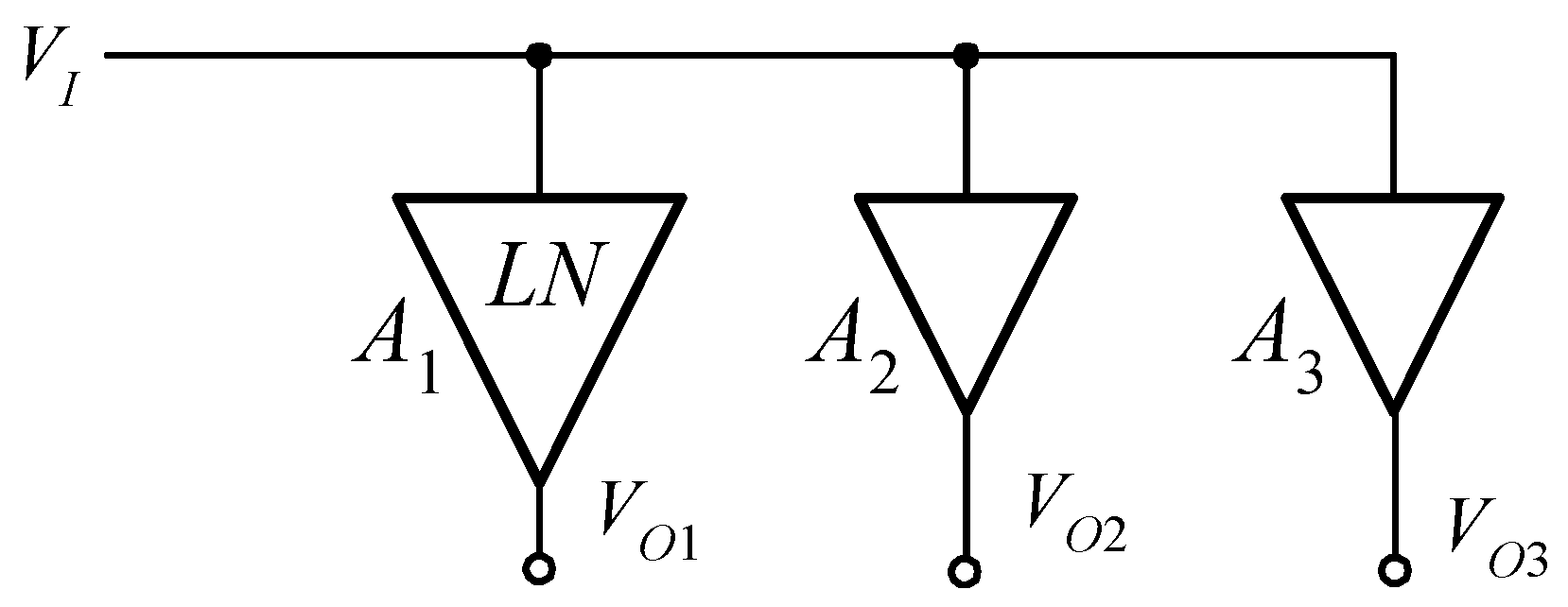
As we have noted before, the main problem with the design we propose is that the passband voltage gain is directly proportional to the transconductance gain gm of the JFET and, therefore, a large spread in the actual value of the gain is to be expected depending on the particular device used in otherwise nominally identical realizations. We believe that for the approach we propose to be feasible in LFNM applications, a sufficiently simple and reliable approach for the calibration of the amplifier gain must be devised. To this end, we propose the approach schematically illustrated in Figure 3.
With reference to Figure 3, the amplifier A1 is a very low noise amplifier designed according to the guidelines discussed above. The other two amplifiers (A2 and A3) are nominally identical OA-based voltage amplifiers with known gain. Since the three amplifiers have their inputs connected together, it is mandatory that the current noise at the inputs of the amplifiers A2 and A3 be as low as possible in order not to degrade the equivalent input current noise (EICN) of the overall system. This can be obtained by resorting to either JFET or MOSFET input OAs that are characterized by extremely low levels of EICN. Typically, low noise JFET input OAs are characterized by a lower level of flicker noise with respect to low noise MOSFET input OAs. However, as it will become clear in the following, for the approach we propose to be effective, we are interested in a low level of voltage noise in the white noise region for A2 and A3. Suppose now that we can perform cross spectra measurements among any two outputs in Figure 3. Let us also assume that such cross spectra estimation is performed in a frequency range in which the voltage gains AV1, AV2, and AV3 of the amplifiers are constant, and their values can be well represented by real numbers. Without loss of generality, we can assume the gains to be positive numbers. Since amplifiers A2 and A3 are identical, AV2 = AV3 = AV. With these assumptions, we would obtain for the cross spectra S12 and S23 between outputsVO1 and VO2 and outputs VO2 and VO3, respectively,
where SI is the power spectral density of the voltage noise at the input of the system. Note that the contribution of the equivalent input voltage noise (EIVN) sources at the inputs of the amplifiers is completely rejected. Since AV is known, independently of the value of SI, Equation (8) can be used to estimate the voltage gain AV1 of the low noise amplifier as follows:
Because of Equation (8), it might be proposed that since the cross spectra approach allows for complete rejection of the contribution of the EIVN of the amplifiers, employing just the two amplifiers A2 and A3 and estimating the cross spectrum S23 is all we need to obtain the PSD of the input noise, without the trouble of resorting to the design in Figure 1. The fact is, however, that the process of estimating cross spectra involves the averaging of the estimated spectra over several time records of the signal to be analyzed. It is indeed the very process of averaging that leads to the cancellation of the uncorrelated noise sources, allowing only the correlated ones to emerge as the number of averages increases [14]. As a general rule, the magnitude of the uncorrelated noise decreases with the square root of the number of averages, i.e., with the number of time records being elaborated. When using a discrete Fourier transform (DFT)-based spectrum analyzer, the duration of each time record is the inverse of the resolution bandwidth Δf that is also the minimum frequency (other than DC) at which the DFT and, hence, spectra and cross spectra can be estimated. Actually, as has been discussed in detail in [26], in the low frequency range, where flicker noise is dominant, the resolution bandwidth needs to be much smaller than the minimum frequency of interest. Suppose now that one is interested in estimating a spectrum at 1 kHz. Employing a very low noise voltage amplifier based on IF3601 [18], one can obtain, at that frequency, a BN less than 1 nV/√Hz (10−18 V2/Hz). If we want to employ a cross correlation configuration using only amplifiers A2 and A3 in the figure, we can obtain an estimate of the time that is required to obtain an equivalent BN of 1 nV starting from the knowledge of their EIVN. Let us assume that A2 and A3 are based on the MOSFET input OA TLC070 (the one that is actually used in our design). The manufacturer lists, for these devices, an EIVN of 7 nV/√Hz (49 × 10−18 V2/Hz) at 1 kHz that is 49 times the EIVN of the low noise amplifier. This means that in order to reduce the equivalent BN by means of cross correlation to the same level of the low noise amplifier, we need about 2500 averages (492). Assuming Δf = 100 Hz << 1 kHz, one time record lasts 10 ms, so that the required measurement time is about 25 s, which can be considered a quite manageable time in most applications. Things change dramatically, however, if we are interested in very low frequencies as in the case of LFNMs on electron devices. Let us assume that fmin = 1 Hz is the minimum frequency of interest (although LFNMs often extend well below 1 Hz). The EIVN of an IF3601-based low noise amplifier can be as low as 1.4 nV/√Hz or 2 × 10⁻¹⁸ V2/Hz [18]. As far as the TLC070 is concerned, although the manufacturer only lists the equivalent input noise down to 10 Hz, since we are well within the flicker region, we can extrapolate the noise at 1 Hz to be about 90 nV/√Hz (≈ 8 × 10⁻¹⁵ V2/Hz), that is, 4 × 10³ times larger than that of the low noise amplifier. As before, we assume that we can employ Δf = fmin/10 = 100 mHz, resulting in a record duration of 10 s. With a factor of 4 × 10³ between the noise of the TLC070 and the one of a good low noise voltage amplifier, we would therefore require a measurement time of 160 × 106 s (about 5 years) to obtain, by cross correlation between the outputs of A2 and A3, a BN equivalent to that of A1. This clearly demonstrates that at very low frequencies, cross correlation is unpractical if the uncorrelated noise to be reduced is large compared to the desired BN. It is therefore important to design voltage amplifiers characterized by intrinsically low equivalent input voltage noise. At the same time, as long as we restrict to frequencies above a few hundred Hz, a few tens of seconds are usually sufficient for obtaining a good estimate of the quantities in Equation (8). In light of these considerations, the approach we propose can be quite effective. As long as we can assume a flat gain for the amplifier A1 at all frequencies of interest, we can perform cross spectra measurement in a conveniently high frequency range so that a correct estimate of the cross spectra in Equation (9) can be obtained in a matter of a few tens of seconds; immediately afterwards, once the actual gain of the low noise amplifier is known, noise measurement at the output VO1 can be started down to the lowest frequency of interest. Typical noise measurements down to frequencies below 1 Hz can last several minutes or several tens of minutes so that the initial measurement session for the calibration of the gain has a very low impact on the overall measurement time, especially because it can be performed with the actual device to be characterized already connected to the measurement system. Moreover, as we shall demonstrate in the section devoted to the experimental results, if proper advanced elaboration approaches are used for spectral estimation, the gain estimation can be obtained as part of the very same measurement session employed for the estimation of the noise produced by the DUT.
A key factor for the application of the approach we propose is the determination of the measurement time required for the correct estimation of the gain according to Equation (9). As we have noted above, the smaller the SI is compared to the equivalent input noise of the amplifiers, the longer the measurement time for obtaining the correct estimation of the gain A1. When performing spectra and cross spectra measurements employing a DFT-based spectrum analyzer, we obtain their estimate at discrete frequencies fk = kΔf, with k being an integer number. Let S11M(fk) and S23M(fk) be the estimates of the cross spectra S11 and S23 in Equation (9) after averaging over M records. Since we assume AV1 to be constant, we can obtain an improved estimate of this parameter by averaging Equation (9) over several frequencies fk as follows:
As will be shown in the next section, the quantity AV1,M can be monitored vs. M (i.e., vs. measurement time) until it stabilizes, at which point its value can be assumed to be the correct estimate of the gain of the low noise amplifier.
3. System Design and Experimental Results
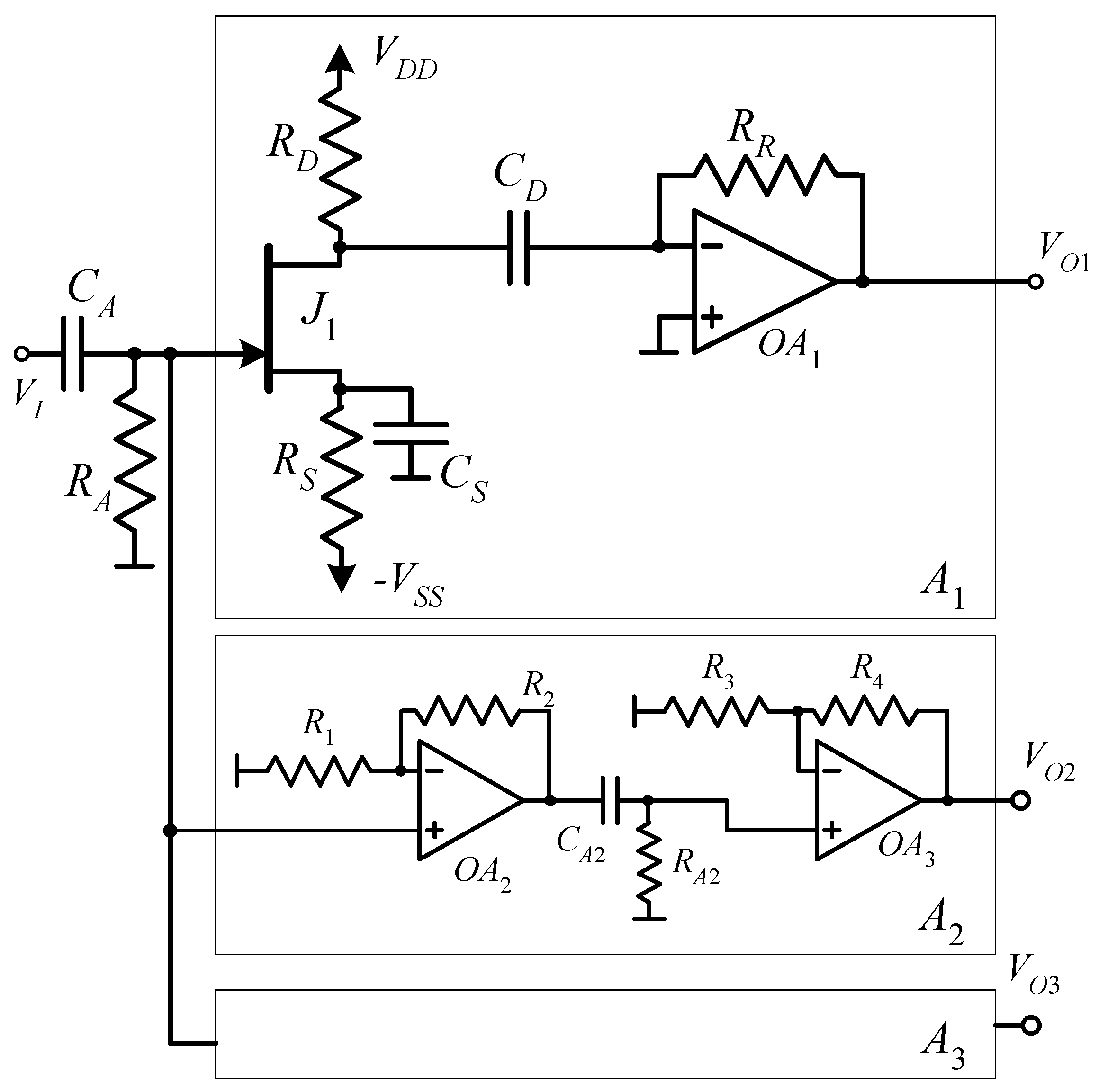
In order to test the effectiveness of the approach we propose, we designed the system reported in Figure 4 following the guidelines discussed in the previous section. The complete component list is reported in Table 1. A single AC coupling filter (CA, RA) is used for removing the DC across the DUT connected to the input. The amplifier A1 is the actual implementation of the circuit in Figure 1, while A2 and A3 are identical two-stage voltage amplifiers with a passband gain of 1111 (61 dB). This is the result of the first (OA2) and second (OA3) stage, having a gain of 11 and 101, respectively.
The higher frequency corner of the amplifier A2 is set by the second stage to about 100 kHz (the gain bandwidth product of OA TLC070 used for OA2 and OA3 is 10 MHz). The AC coupling network CA2–RA2, that removes the DC introduced by the offset of the first stage, introduces a low frequency corner at about 16 mHz that, in combination with the input AC filter (CA, RA), sets the lower frequency corner for the response from the input to the output VO2. Since the auxiliary amplifiers A2 and A3 are only used for gain calibration (frequency range of interest above a few hundred Hz) the time constant CA2RA2 is not critical. From the point of view of the input of the system, the connection of the inputs of the amplifiers A2 and A3 to the gate of the JFET results in a negligible contribution in terms of current noise (the equivalent input current noise for the TLC070 is 0.6 fA/√Hz) and in a contribution of a few tens of pF to the input capacitance of the system that is, however, dominated by the JFET (the typical gate to source and gate to drain capacitances for the IF3601 are 300 and 200 pF, respectively). As far as the low noise amplifier is concerned, the JFET is biased in such a way as to obtain a drain current of about 2.5 mA and a drain to source voltage of about 2 V, sufficient to ensure operation in the active region. In these bias conditions, we expect to obtain a transconductance in the range from 20 to 50 mA/V. As far as the frequency response is concerned, there are three pole frequencies to be set, one of which—the one associated with CS—depends on the value of the transconductance gm. With a target passband extending well below 1 Hz, we must ensure that all pole frequencies are well below this limit. With the values of the parameters in Table 1, the pole frequency associated to CS remains below 10 mHz regardless of the value of gm in the range from 20 to 50 mA/V. The pole associated to CA is set at 2 mHz, while the pole associated to CD is set at 10 mHz with these values, regardless of the actual frequency of the pole due to CS, we can expect an essentially flat response above 200 mHz. Depending on the value of gm, with RR = 50 kΩ, the passband gain of the low noise amplifier ranges from 60 up to 68 dB (from 1000 up to 2500).
The actual prototype that was implemented and used for testing is shown in Figure 5. The yellow line superimposed to the picture represents the wiring that needs to be added to connect the gate of the JFET J1 to the inputs of the amplifiers A2 and A3 as in Figure 4. Removing the yellow connection allowed to test each amplifier independently of the others. A block diagram of the measurement setup is also shown in Figure 6. The amplifier, together with the battery pack for its supply and the DUT, as is typically the case in LFNMs, is enclosed in aluminum box that acts as a shield with respect to interferences coming from the environment. The DUTs used for the test experiments are simple resistors, but in the case of noise measurement on electron devices, the bias system for the device would also typically be contained in the shielded box. Three BNC connectors are used to allow connection from the outputs of the amplifiers (VO1, VO2, and VO3) to the input of the acquisition and elaboration system.
As shown in Figure 6, for the acquisition and elaboration of the output signals, we resorted to a National Instruments 4-channel DSA board (PCI 4462) and dedicated software developed around the public domain library QLSA [27]. While the development of dedicated software is not mandatory, as we have discussed in the previous paragraph, resorting to the QLSA library in this specific application can be extremely convenient. As discussed in [27], QLSA operates very much like a large number of conventional DFT spectrum analyzers all receiving the same input signal, but with each one operating with the same record length but in a different frequency range and, hence, with a different resolution bandwidth. In particular, at higher frequencies, the resolution bandwidth is larger, resulting in time records with shorter duration, while at lower and lower frequencies, the resolution bandwidth is proportionally reduced. All these virtual analyzers operate in parallel, and this means, with reference to the calibration approach we propose, that the higher frequency ranges can be exploited for the calibration of the gain according to the procedure discussed in the previous paragraph while, at the same time, power spectra estimation at the output VO1 can proceed with the proper (small) Δf required to correctly estimate power spectra in the frequency range below 1 Hz.
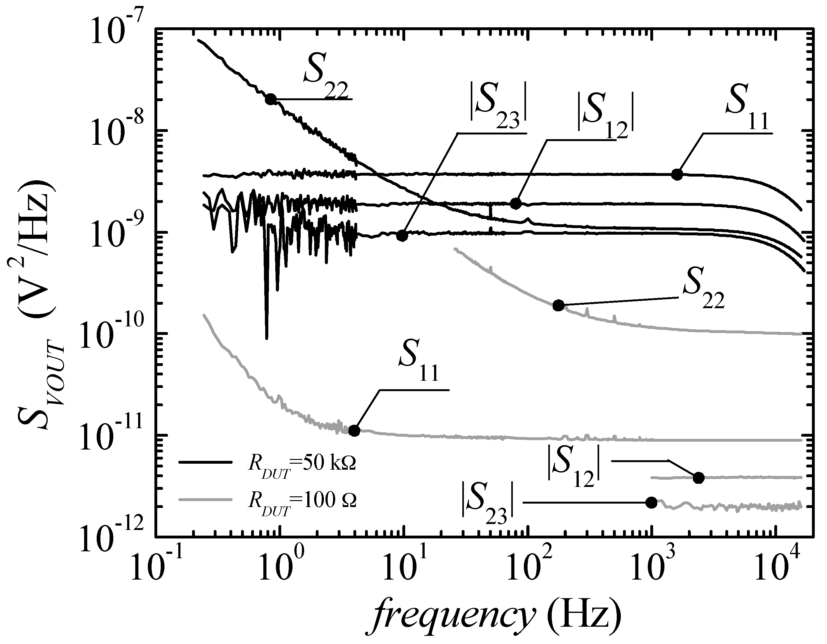
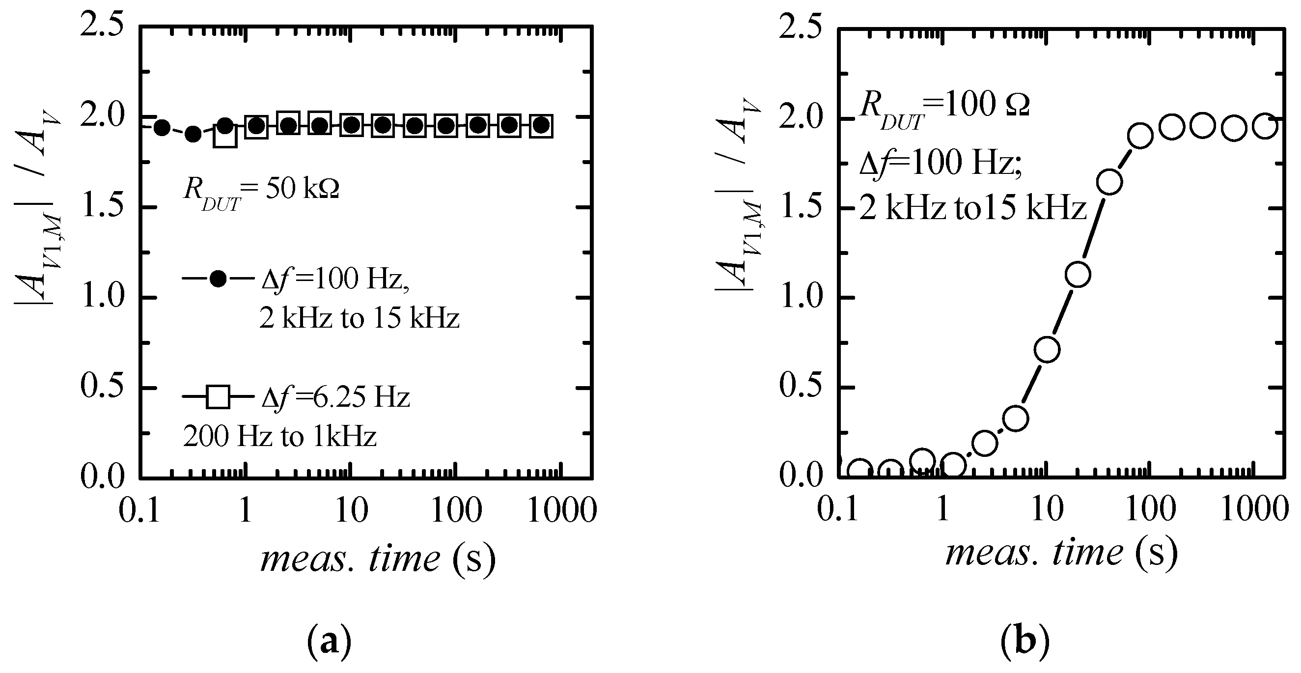
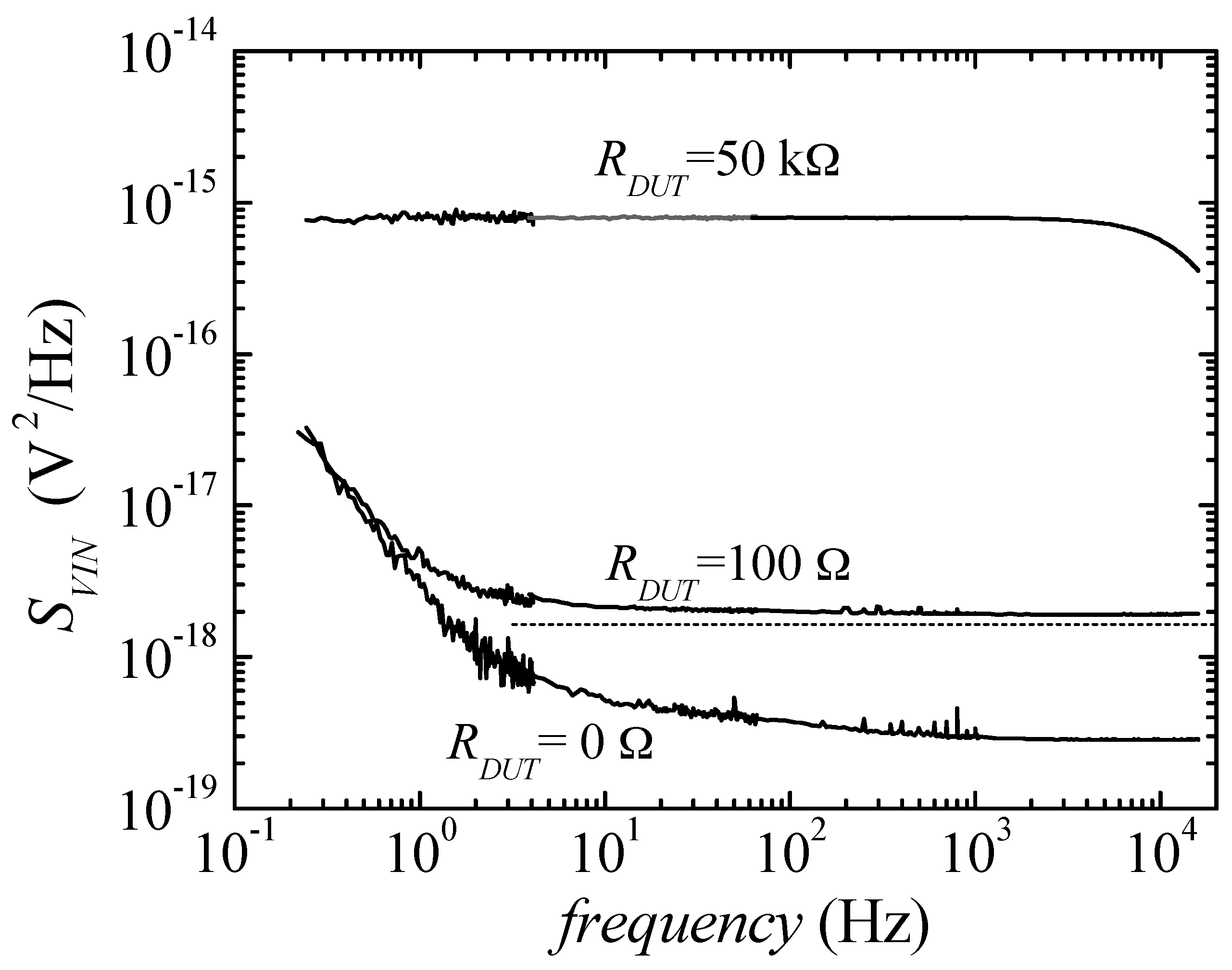
As a first test experiment, we used an unbiased 50 kΩ resistor as a DUT at the input of the system. The thermal noise of a 50 kΩ resistor at room temperature is about 29 nV/√Hz (8.3 × 10⁻¹⁶ V2/Hz) and it is, therefore, much larger than the expected equivalent input voltage noise of the low noise amplifier in the entire frequency range of interest. Hence, regardless of the actual value of the gain, the spectrum at the output VO1 can be used to verify the shape of the frequency response. The result of the estimation of the PSD of the noise at the output VO1 is reported in Figure 7 (black curve labeled S11). As can be verified, the curve is flat, indicating a constant frequency response from 200 mHz up to above 1 kHz, after which the PSD decreases. However, this decrease can be traced back to the low pass filtering effect due to the capacitance at the input of the JFET that, in the passband and in the configuration in Figure 4, is essentially the sum of the gate-to-source and of the gate-to-drain capacitances of the device, in the order of 500 pF. Indeed, an RC low pass filter with R = 50 kΩ (the resistance of the DUT at the input) and C = 500 pF would result in a pole frequency of about 6.4 kHz, consistent with the behavior for S11 observed in Figure 7. All spectra and cross spectra shown in Figure 7 are obtained by resorting to QLSA. The sampling frequency is 51.2 kHz. In the uppermost frequency range (above 1 kHz), the resolution bandwidth Δf is 100 Hz, while in the lowest frequency range, Δf = 25 mHz. In order to obtain very smooth spectra at very low frequencies, averaging for the spectra in Figure 7 was carried on for about 2 h. However, the correct estimate of the gain AV1 was obtained just after a few seconds, as confirmed from the plot of |AV1,M| vs. time in Figure 8a.
To verify the robustness of the approach we propose, the estimation of AV1,M was carried out over two frequency ranges. The circles in Figure 8a are relative to the estimation of the gain performed in the frequency range from 200 Hz to 1 kHz (with Δf = 6.25 Hz) where the recorded spectra appear to be flat, while the squares are relative to the estimation of the gain in the frequency range from 2 to 15 kHz (with Δf = 100 Hz), where SI, regarded as the noise at the input of the gate of the JFET, changes with frequency because of the filtering effect due to the input capacitance of the amplifier combined with the resistance of the DUT, as previously discussed. A careful observation of Figure 8a indicates that the time required for the correct estimation of AV1 is shorter, as expected, in the case of the estimation with the larger resolution bandwidth. In any case, after 20 seconds, the two estimates essentially coincide (AV1 = 2160), with a difference between the two of less than 0.3%. This result also demonstrates that the gain from the gate of the JFET toward the output is flat up to frequencies well above 10 kHz. Note that the ability to obtain the correct estimate of the gain after a few seconds, also in the case of a relatively small Δf, is due to the fact that the noise introduced by the DUT is also large with respect to the EIVN of the amplifiers A2 and A3 in the frequency range in which the gain estimation was performed. In order to test our approach in a much more demanding case, we used a 100 Ω resistance as a DUT. The thermal noise of a 100 Ω resistor at room temperature is about 1.29 nV/√Hz (≈1.66 × 10⁻¹⁸ V2/Hz). In terms of PSD, this noise level is about 30 times smaller than the EIVN of A2 and A3 for f = 1 kHz, and it is in the same order of magnitude of the BN of the best low noise amplifiers for LFNM applications. The spectra obtained in this case, in the same measurement conditions as before, are reported in Figure 7 (gray curves). To avoid complicating the figure, the plot of the cross spectra is, in this case, shown only in the highest frequency range, that is, the one used for gain calibration. The behavior of AV1,M vs. time is shown in Figure 8b. As can be noted, in this situation, since SI is very small compared to the EIVN of A2 and A3 even at higher frequencies, we need to wait a few minutes before reaching the situation in which the estimated value no longer changes with time. In any case, after 2 min, the estimated value sets are within ±2% of the asymptotic value. Therefore, even in this demanding situation, we obtain the conclusion that a quite good estimate of the amplifier gain can be reached in a fraction of the time required for the measurement of the DUT noise.
With the value of the calibrated gain as obtained from Figure 8, we obtain the equivalent noise at the input of the amplifier, as reported in Figure 9. Note that our approach requires a DUT to generate noise that is present at the input of the amplifier to calibrate the gain. In order to evaluate the BN of the low noise amplifier, that is, the equivalent input noise when the input is shorted, we used the value of the gain obtained in the case in which the DUT was a 100 Ω resistance. To ensure that no appreciable change in the gain could occur, the measurement with the shorted input was performed immediately after the measurement with a 100 Ω DUT was completed. As can be noted in Figure 9, the low noise amplifier is characterized by excellent noise performances, especially when we take into account its very simple structure. The EIVN at 200 mHz is about 6 nV/√Hz and becomes less than 1 nV/√Hz above 2 Hz.
While the main purpose of this work was to demonstrate the effectiveness of the approach we propose, it is worth noting that the performances of the amplifier we have designed, in terms of EIVN, compare very well with other designs resorting to the IF-3601 as the active device. A comparison with two of such designs is summarized in Table 2.
The design in [22] relies on a single JFET stage and requires either dedicated measurements for gain calibration or acting on a variable component in the circuit for gain adjustment. As can be noted, noise performances are essentially comparable, notwithstanding the fact that the bias current for the JFET in our design is smaller than the one used in [22] (the equivalent input noise for a JFET decreases for increasing bias current). The design in [18] relies on a feedback configuration employing an IF 3602 (a pair of IF3601 in a single device) for the differential input stage. In this case, we can observe a lower level of noise in the proposed design for a lower bias current. It must be noted that at higher frequencies, the EIVN in [18] increases as a result of the effect of the compensation network employed to insure stability. In any case, what we believe sets our approach apart from others is its degree of flexibility. The fact that we do not resort to a feedback configuration greatly simplifies the design of the low noise amplifier. Different JFETs with different characteristics of noise and input capacitances can be used to quickly and effectively design the low noise amplifier: the same measurement configuration, with the same auxiliary amplifiers can be used for obtaining gain calibration while performing measurements. In the same way, different OAs can be used for the auxiliary amplifiers as long as they are characterized by low input noise current. While the auxiliary amplifiers are used at higher frequencies, resorting to JFET input OAs that have lower low frequency corners would allow, in many cases, a reduction in the time required for gain calibration by extending the frequency interval used for the estimation of the gain toward lower frequencies according to Equation (10). As a final remark, it must be noted that the gain calibration approach we propose works as long as the noise level introduced by the DUT in the frequency interval used for gain estimation is non-negligible. In the rare situations in which this condition cannot be satisfied, we would, however, not be worse off than in the case of the amplifier in [22], with the advantage that the presence of the auxiliary amplifiers would still allow the measurement of the gain of the low noise amplifier by connecting a simple resistor at the input of the system prior to the measurement on the actual DUT.
4. Conclusions
We proposed an approach for the design of low noise voltage preamplifiers for application in the field of low frequency noise measurements on electron devices. We resorted to an open loop design for the amplifier front-end with the advantage of reducing the number of active components introducing noise and avoiding compensation networks for insuring stability. We have demonstrated remarkable noise performance with an extremely simple and compact design (only 9 components for the main amplifier, including the coupling networks). The problem of gain calibration, which is typical of an open loop design, has been successfully addressed by introducing two simple auxiliary OA-based voltage amplifiers with stable and known gain and resorting to cross correlation to extract the amplifier gain, even while actual measurements on a DUT are in progress.
Author Contributions
Conceptualization, G.S., and C.C.; methodology, G.S. and C.C.; software, C.C.; validation, G.G.; formal analysis, G.G. and C.C.; investigation, G.S.; data curation, C.C.; writing—original draft preparation, G.S. and C.C.
Funding
This research received no external funding.
Conflicts of Interest
The authors declare no conflict of interest.
References
- Deen, M.J.; Pascal, F. Electrical characterization of semiconductor materials and devices. J. Mater. Sci.-Mater. Electron. 2006, 43, 585–599. [Google Scholar] [CrossRef]
- Wong, H. Low-frequency noise study in electron devices: Review and update. Microelectron. Reliab. 2003, 43, 585–599. [Google Scholar] [CrossRef]
- Rao, H.; Bosman, G. Device reliability study of AlGaN/GaN high electron mobility transistors under high gate and channel electric fields via low frequency noise spectroscopy. Microelectron. Reliab. 2010, 50, 1528–1531. [Google Scholar] [CrossRef]
- Labat, N.; Malbert, N.; Maneux, C.; Touboul, A. Low frequency noise as a reliability diagnostic tool in compound semiconductor transistors. Microelectron. Reliab. 2004, 44, 1361–1368. [Google Scholar] [CrossRef]
- Fleetwood, D.M. 1/f Noise and Defects in Microelectronic Materials and Devices. IEEE Nucl. Plasma Sci. 2015, 62, 1462–1486. [Google Scholar] [CrossRef]
- Min, B.; Devireddy, S.P.; Çelik-Butler, Z.; Shanware, A.; Colombo, L.; Green, K.; Chambers, J.J.; Visokay, M.R.; Rotondaro, A.L.P. Impact of Interfacial Layer on Low-Frequency Noise of HfSiON Dielectric MOSFETs. IEEE Trans. Electron. Dev. 2006, 53, 1459–1466. [Google Scholar] [CrossRef]
- Renteria, J.; Samnakay, R.; Rumyantsev, S.L.; Jiang, C.; Goli, P.; Shur, M.S.; Balandin, A.A. Low-frequency 1/f noise in MoS2 transistors: Relative contributions of the channel and contacts. Appl. Phys. Lett. 2014, 104, 153104. [Google Scholar] [CrossRef]
- Giusi, G.; Giordano, O.; Scandurra, G.; Calvi, S.; Fortunato, G.; Rapisarda, M.; Mariucci, L.; Ciofi, C. Correlated Mobility Fluctuations and Contact Effects in p-Type Organic Thin-Film Transistors. IEEE Trans. Electron. Dev. 2016, 63, 1239–1245. [Google Scholar] [CrossRef]
- Hossain, M.Z.; Rumyantsev, S.; Shur, M.S.; Balandin, A.A. Reduction of 1/f noise in graphene after electron-beam irradiation. Appl. Phys. Lett. 2013, 102, 153512. [Google Scholar] [CrossRef]
- Smulko, J.M.; Trawka, M.N.; Granqvist, C.G.; Ionescu, R.D.; Annanouch, F.D.; Llobet, E.D.; Kish, L.B. New approaches for improving selectivity and sensitivity of resistive gas sensors: A review. Sens. Rev. 2015, 4, 340–347. [Google Scholar] [CrossRef]
- Aleeva, Y.; Maira, G.; Scopelliti, M.; Vinciguerra, V.; Scandurra, G.; Cannata, G.; Giusi, G.; Ciofi, C.; Figa, V.; Occhipinti, L.G.; et al. Amperometric Biosensor and Front-End Electronics for Remote Glucose Monitoring by Crosslinked PEDOT-Glucose Oxidase. IEEE Sens. J. 2018, 18, 4869–4878. [Google Scholar] [CrossRef] [Green Version]
- Kish, L.B.; Vajtai, R.; Granqvist, C.G. Extracting information from noise spectra of chemical sensors: Single sensor electronic noses and tongues. Sensor Actuat. B-Chem. 2000, 71, 55–59. [Google Scholar] [CrossRef]
- Sampietro, M.; Fasoli, L.; Ferrari, G. Spectrum analyzer with noise reduction by cross-correlation technique on two channels. Rev. Sci. Instrum. 1999, 70, 2520–2525. [Google Scholar] [CrossRef]
- Scandurra, G.; Giusi, G.; Ciofi, C. Multichannel amplifier topologies for high-sensitivity and reduced measurement time in voltage noise measurements. IEEE Trans. Instrum. Meas. 2013, 62, 1145–1153. [Google Scholar] [CrossRef]
- Ciofi, C.; Scandurra, G.; Merlino, R.; Cannatà, G.; Giusi, G. A new correlation method for high sensitivity current noise measurements. Rev. Sci. Instr. 2007, 78, 114702. [Google Scholar] [CrossRef]
- Analog Devices, SSM2220: Audio Dual Matched PNP Transistor. Available online: https://www.analog.com/media/en/technical-documentation/data-sheets/SSM2220.pdf (accessed on 10 September 2019).
- Neri, B.; Pellegrini, B.; Saletti, R. Ultra Low-Noise Preamplifier for Low-Frequency Noise Measurements in Electron Devices. IEEE Trans. Instrum. Meas. 1991, 40, 2–6. [Google Scholar] [CrossRef]
- Cannatà, G.; Scandurra, G.; Ciofi, C. An ultralow noise preamplifier for low frequency noise measurements. Rev. Sci. Instr. 2009, 80, 114702. [Google Scholar] [CrossRef]
- Scandurra, G.; Cannatà, G.; Ciofi, C. Differential ultralow noise amplifier for low frequency noise measurements. AIP Adv. 2011, 1, 022144. [Google Scholar] [CrossRef]
- Ciofi, C.; Giusi, G.; Scandurra, G.; Neri, B. Dedicated instrumentation for high sensitivity, low frequency noise measurement systems. Fluct. Noise Lett. 2004, 4, 385–402. [Google Scholar] [CrossRef]
- Giusi, G.; Cannatà, G.; Scandurra, G.; Ciofi, C. Ultra-low-noise large-bandwidth transimpedance amplifier. Int. J. Circ. Theor. Appl. 2015, 43, 1455–1473. [Google Scholar] [CrossRef]
- Levinzon, F.A. Ultra-low-noise high-input impedance amplifier for low-frequency measurement applications. IEEE Trans. Circuits Syst. I 2008, 55, 1815–1822. [Google Scholar] [CrossRef]
- Scandurra, G.; Cannatà, G.; Giusi, G.; Ciofi, C. Programmable, very low noise current source. Rev. Sci. Instr. 2014, 85, 125109. [Google Scholar] [CrossRef] [PubMed]
- Ivanov, V.E.; Chye, E.U. Simple programmable voltage reference for low frequency noise measurements. J. Phys. Conf. Ser. 2018, 1015, 052011. [Google Scholar] [CrossRef]
- Scandurra, G.; Giusi, G.; Ciofi, C. A very low noise, high accuracy, programmable voltage source for low frequency noise measurements. Rev. Sci. Instr. 2014, 85, 044702. [Google Scholar] [CrossRef] [PubMed]
- Giusi, G.; Scandurra, G.; Ciofi, C. Estimation errors in 1/f γ noise spectra when employing DFT spectrum analyzers. Fluct. Noise Lett. 2013, 12, 1350007. [Google Scholar] [CrossRef]
- Ciofi, C.; Scandurra, G.; Giusi, G. QLSA: A Software Library for Spectral Estimation in Low-Frequency Noise Measurement Applications. Fluct. Noise Lett. 2019, 18, 1940004. [Google Scholar] [CrossRef]
Figure 1.
Reference schematic of a JFET CS stage-based amplifier. The second stage (transimpedance amplifier (TIA)) represents the idealized behavior of an operational amplifier-based transimpedance amplifier with gain AR.
Figure 1.
Reference schematic of a JFET CS stage-based amplifier. The second stage (transimpedance amplifier (TIA)) represents the idealized behavior of an operational amplifier-based transimpedance amplifier with gain AR.

Figure 2.
Small signal equivalent circuit of the amplifier in Figure 1. All relevant noise sources are shown in the figure. The noise sources enRX account for the thermal noise introduced by the resistances RX; the source enj is used to model the noise introduced by the JFET; the source int is used to model the noise introduced by the transimpedance amplifier (TIA).

Figure 3.
Amplifier configuration for gain calibration. A1 is the low noise (LN) amplifier in Figure 1; A2 and A3 are operational amplifier (OA)-based amplifiers with stable and known gain.
Figure 3.
Amplifier configuration for gain calibration. A1 is the low noise (LN) amplifier in Figure 1; A2 and A3 are operational amplifier (OA)-based amplifiers with stable and known gain.

Figure 4.
Detailed schematic of the low noise amplifier (A1) together with the two identical auxiliary amplifiers (A2, A3) required for gain calibration by means of cross correlation measurements. The detailed component list is reported in Table 1.
Figure 4.
Detailed schematic of the low noise amplifier (A1) together with the two identical auxiliary amplifiers (A2, A3) required for gain calibration by means of cross correlation measurements. The detailed component list is reported in Table 1.

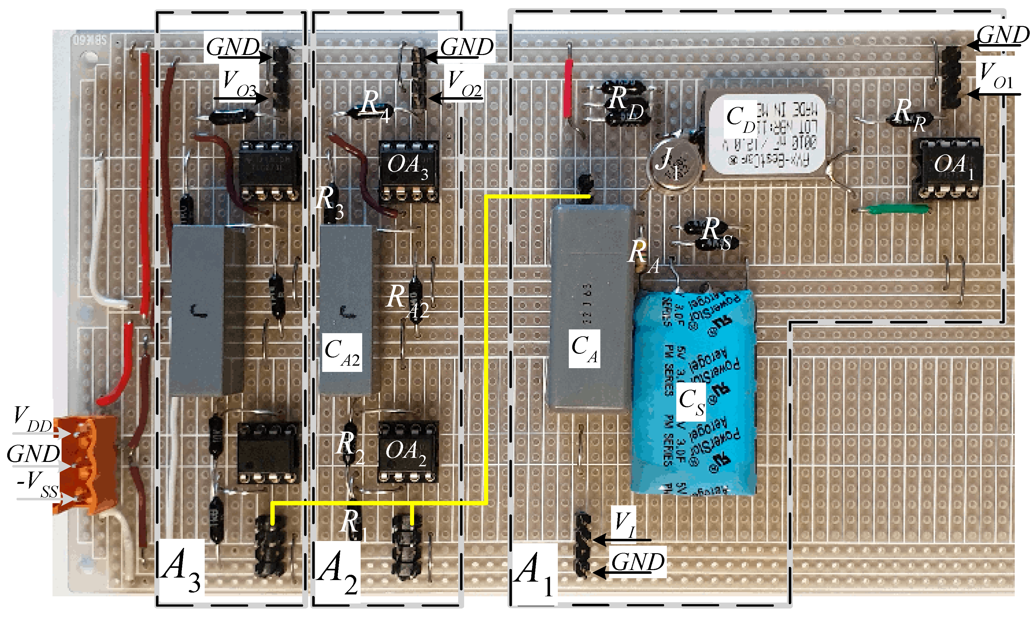
Figure 5.
Top view of the implementation of the circuit in Figure 4. All components of amplifiers A1 and A2 are labeled with the same names used in Figure 4. The yellow path shows the connection that needs to be made to connect the gate of the JFET to the inputs of A2 and A3.

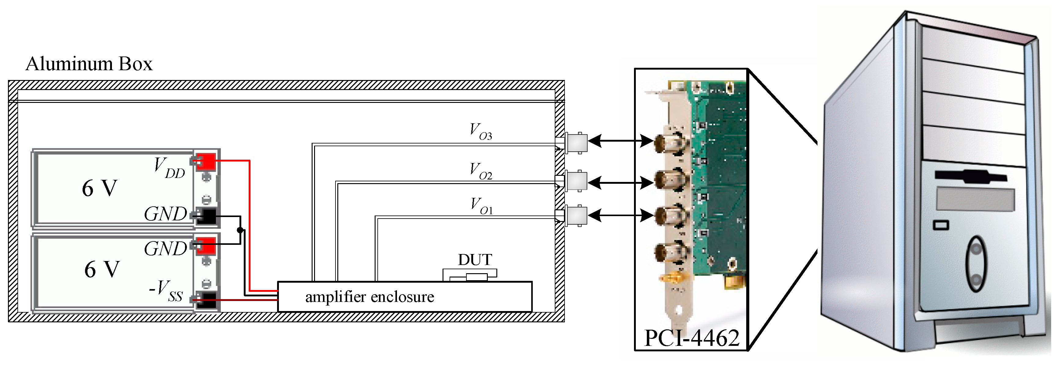
Figure 6.
Block diagram of the measurement setup. Two lead acid 6 V batteries are used to supply the amplifier. The batteries, the amplifier and the DUT are all located inside an aluminum box that acts as a shield against external interferences.
Figure 6.
Block diagram of the measurement setup. Two lead acid 6 V batteries are used to supply the amplifier. The batteries, the amplifier and the DUT are all located inside an aluminum box that acts as a shield against external interferences.

Figure 7.
Cross spectra at the outputs VO1, VO2, and VO3 in Figure 4. The black curves are obtained with RDUT = 50 kΩ; the gray curves refer to the case RDUT = 100 Ω. S11 is the power spectral density (PSD) at the output of the low noise amplifier (A1); S22 is the PSD at the output of one of the auxiliary amplifiers (A2); S12 is the cross spectrum between the low noise amplifier (A1) and one of the auxiliary amplifiers (A2); S23 is the cross spectrum between the outputs of the two auxiliary amplifiers.

Figure 8.
Gain of the low noise amplifier (AV1,M) normalized with respect to the gain AV of the auxiliary amplifiers vs. measurement time according to Equation (10). The plot on the left (a) refers to the case RDUT = 50 kΩ; the plot on the right (b) refers to the case RDUT = 100 Ω.
Figure 8.
Gain of the low noise amplifier (AV1,M) normalized with respect to the gain AV of the auxiliary amplifiers vs. measurement time according to Equation (10). The plot on the left (a) refers to the case RDUT = 50 kΩ; the plot on the right (b) refers to the case RDUT = 100 Ω.

Figure 9.
Referred noise obtained dividing the noise at the output VO1 by the calibrated gain squared. In the case of RDUT = 100, the measured noise is above the ideal one because at these low levels of noise, the background noise (BN) is no longer negligible.
Figure 9.
Referred noise obtained dividing the noise at the output VO1 by the calibrated gain squared. In the case of RDUT = 100, the measured noise is above the ideal one because at these low levels of noise, the background noise (BN) is no longer negligible.


Table 1.
List for the circuit in Figure 3.
Table 1.
List for the circuit in Figure 3.
| Component | Type | Value |
|---|---|---|
| J1 | Low noise discrete JFET | IF3601 |
| VDD, VSS | 4 Ah, lead acid batteries | 6 V |
| OA1, OA2, OA3 | MOSFET input, low noise OA | TLC070 |
| RA | 1% metallic film resistor | 3.3 MΩ |
| RS | 2 × 5 kΩ, 1/8 W, 0.1% metallic film in parallel 1 | 2.5 kΩ |
| RD | 3 × 5 kΩ, 1/8 W, 0.1% metallic film in parallel 1 | 1.67 kΩ |
| RR | 0.1% metallic film resistor | 50 kΩ |
| CA | Polyester, 66 V | 22 μF |
| CS | Supercapacitor, 5V | 3 F |
| CD | Supercapacitor, 12 V | 10 mF |
| R1, R3 | 0.1% metallic film resistor | 1 kΩ |
| R2 | 0.1% metallic film resistor | 10 kΩ |
| R4 | 0.1% metallic film resistor | 100 kΩ |
| CA2 | Polyester, 66 V | 10 μF |
| RA2 | 1% metallic film resistor | 1 MΩ |
1 Resistors are in parallel to minimize flicker noise [17].
Table 2.
Comparison of the prototype in this work with other works.
| ULNA | Equivalent Input Voltage Noise (nV/√Hz) | JFET Bias Current | Offline Cal. * | |||||
|---|---|---|---|---|---|---|---|---|
| 200 mHz | 1 Hz | 10 Hz | 100 Hz | 1 kHz | 10 kHz | |||
| This work | 6 | 1.7 | 0.7 | 0.6 | 0.5 | 0.5 | 2.5 mA | NO |
| Levinzon [22] | 4 | 1.4 | 0.6 | 0.6 | 0.5 | 0.5 | 5 mA | YES |
| Cannatà et al. [18] | 6 | 1.4 | 1 | 0.9 | 0.8 | 1.1 | 4 mA | NO |
* Gain calibration must be performed with a dedicate measurement with a calibrated source.
© 2019 by the authors. Licensee MDPI, Basel, Switzerland. This article is an open access article distributed under the terms and conditions of the Creative Commons Attribution (CC BY) license (http://creativecommons.org/licenses/by/4.0/).
Share and Cite
MDPI and ACS Style
Scandurra, G.; Giusi, G.; Ciofi, C. Single JFET Front-End Amplifier for Low Frequency Noise Measurements with Cross Correlation-Based Gain Calibration. Electronics 2019, 8, 1197. https://doi.org/10.3390/electronics8101197
AMA Style
Scandurra G, Giusi G, Ciofi C. Single JFET Front-End Amplifier for Low Frequency Noise Measurements with Cross Correlation-Based Gain Calibration. Electronics. 2019; 8(10):1197. https://doi.org/10.3390/electronics8101197
Chicago/Turabian StyleScandurra, Graziella, Gino Giusi, and Carmine Ciofi. 2019. "Single JFET Front-End Amplifier for Low Frequency Noise Measurements with Cross Correlation-Based Gain Calibration" Electronics 8, no. 10: 1197. https://doi.org/10.3390/electronics8101197
Note that from the first issue of 2016, this journal uses article numbers instead of page numbers. See further details here.