Dual-Input Isolated DC-DC Converter with Ultra-High Step-Up Ability Based on Sheppard Taylor Circuit


Department of Electronic Engineering, National Kaohsiung University of Science and Technology, Kaohsiung City 82445, Taiwan
*
Author to whom correspondence should be addressed.
Electronics 2019, 8(10), 1125; https://doi.org/10.3390/electronics8101125
Submission received: 8 September 2019
/
Revised: 4 October 2019
/
Accepted: 5 October 2019
/
Published: 7 October 2019
(This article belongs to the Special Issue Intelligent Electronic Devices)
Abstract
:A dual-input high step-up isolated converter (DHSIC) is proposed in this paper, which incorporates Sheppard Taylor circuit into power stage design so as to step up voltage gain. In addition, the main circuit adopts boosting capacitors and switched capacitors, based on which the converter voltage gain can further be improved significantly. Since the proposed converter possesses an inherently ultra-high step-up feature, it is capable of processing low input voltages. The DHSIC also has the important features of leakage energy recycling, switch voltage clamping, and continuous input-current obtaining. These characteristics advantage converter efficiency and benefit the DHSIC for high power applications. The structure of the proposed converter is concise. That is, it can lower cost and simplifies control approach. The operation principle and theoretical derivation of the proposed converter are discussed thoroughly in this paper. Simulations and hardware implementation are carried out to verify the correctness of theoretical analysis and to validate feasibility of the converter as well.
1. Introduction
Nowadays, electricity is mostly generated by fossil fuels and nuclear fuel. Although nuclear power plants can generate considerable power by utilizing a little amount of nuclear fuel, nuclear waste influencing the environment is inevitable. Fossil fuels have been overused and become in shortage. Therefore, human beings attempt to discover more alternatives for maintaining global economic development and environment protection. To alleviate the problems of global temperature rising and serious greenhouse gas emission, many kinds of clean-energy power generation, such as photovoltaic (PV) panel, wind turbine, and fuel-cell stack, are developed imperatively [1,2].
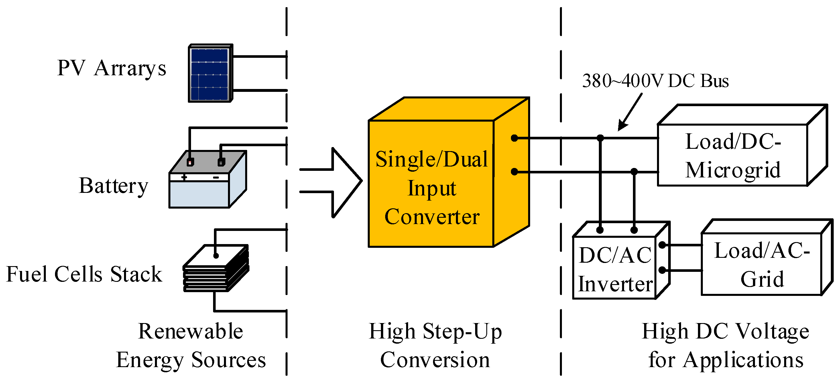
In general, renewable power systems need a DC-bus voltage in the range of 380 V–400 V for grid-tied connection or in high power applications. Unfortunately, the output voltage of a PV module, battery or fuel cell is much lower than the dc-bus voltage and thus conventional DC/DC converters cannot be utilized directly to serve as an energy interface for dealing with power control. In addition, if the power supplied from two input ports has to be processed simultaneously, dual-input converter with high voltage gain is essentially anticipated. Figure 1 illustrates a hybrid generation system that includes two sources, a high step-up converter, and an inverter for AC application, which reveals that a dual-input converter with high step-up voltage gain is urgent in such system.
Theoretically, conventional step-up converters, like Boost and Flyback [3,4,5,6], can achieve a high voltage gain under the operating with extremely high duty ratio or the design of a much higher turns ratio. However, extreme high duty cycle or turns ratio will dramatically degrade the conversion efficiency due to large conduction loss and copper loss of windings. In order to improve conversion efficiency and voltage gain, many transformerless high step-up converters are proposed [7,8,9,10]. Although these converters are designed to achieve high step-up characteristics with reasonable duty ratio, here still exits some problems, for instance, large transient current and limited voltage gain, confining converter flexibility. To mitigate the mentioned drawbacks, converters incorporating coupled inductor and/or switched capacitor are proposed [11,12,13,14], however, which are only able to process single-input source. In order to deal with two different kinds of inputs, dual-input converters (DIC) are proposed. In comparison with single input, a dual generation system is capable of providing higher reliability, durability and power rating. The structure of DICs can be simply classified as series type and parallel one. The conventional series-type DICs construct string connection at input ports [15,16]. Such a DIC will malfunction in case that either of the two inputs fails. The parallel-type DICs collocate different sources in parallel so that even if one of the inputs is out of commitment, it still can accomplish voltage stepping to meet DC-bus level [17,18,19,20,21,22,23]. Some of them are controlled with time-sharing scheme. That is, only one DC source is permitted to delivery its energy to the load at a time. Compared with series-type DICs, parallel ones possess much better features from the aspects of reliability and controllability. Nevertheless, limitation on voltage gain is unavoidable, which confines converter applications in the field of high DC-bus voltage requirement.
In order to convert a lower DC voltage to a much higher level and to provide consecutive power even under the situation that one input source shuts down, this paper proposes a DHSIC, which is developed by means of boosting capacitor, switched capacitor and Sheppard Taylor circuit. The proposed dual-input converter can achieve the following important features: ultra-high step-up ability, continuous input current, and galvanic isolation. Furthermore, the proposed converter possesses the competence of inherent voltage clamping without any additional devices and recycling leakage energy stored in transformers. Therefore, the voltage spike on the power switch can be suppressed and converter efficiency is also improved.
The structure of this paper is organized as follows. Following the introduction, the operation principle of the proposed dual-input high step-up isolated converter is described in Section 2. The steady-state analysis is discussed in Section 3, which covers voltage gain of the converter, voltage and current stresses of the semiconductor device, and magnetizing inductance design in continuous conduction mode (CCM). To verify the correctness of proposed converter, experimental results from a 200-W prototype are illustrated in Section 4. Finally, Section 5 summarizes the conclusions of this paper.
2. Operation Principle of Proposed Dual-Input Converter
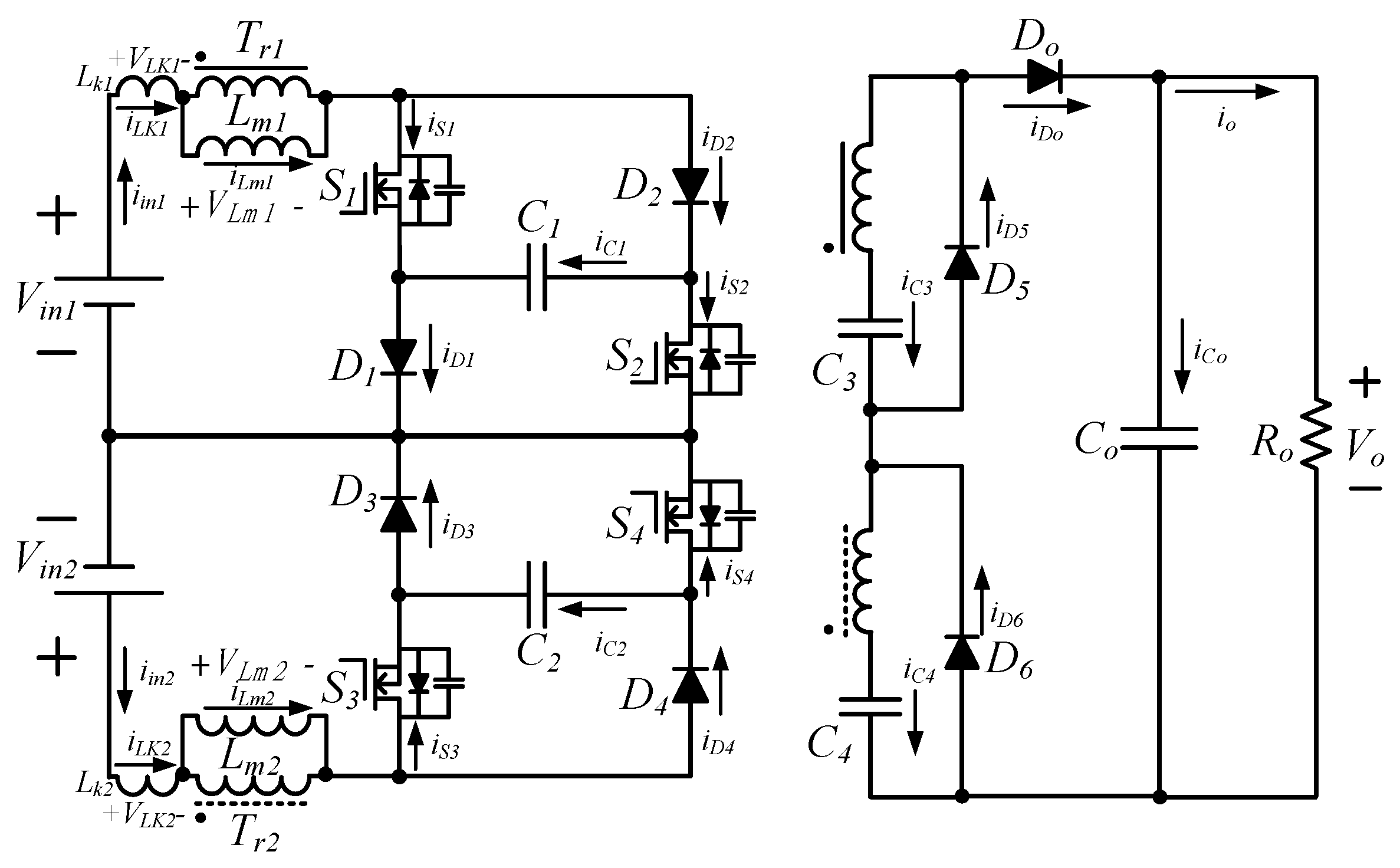
The equivalent of the proposed DHSIC is shown in Figure 2. Parameters in Figure 2 are represented in the following. Vin1 and Vin2 are input voltages, while iin1 and iin2 denote input currents. The practical model of coupled inductor includes magnetizing inductance, leakage inductance, and an ideal transformer. The Lm1 and Lm2 are the magnetizing inductances of T1 and T2, respectively, meanwhile, leakage inductances are expressed as Lk1 and Lk2. The S1–S4 represent the four main power switches. The C1 and C2 function as boosting capacitors, and C3 and C4 serve as switched capacitors. These capacitors can elevate converter voltage gain effectively. The D1–D6 are rectifier diodes. In addition, Do and Co are the output diode and filter capacitor, respectively. Output voltage and current of DHSIC are in turn described as Vo and Io. Finally, the output equivalent resistance is presented as Ro. Even though the proposed DHSIC works normally in dual input operation (DIO), it still possesses the ability to be in single-input operation (SIO) while either input source fails. In Section 2, DIO will be first discussed followed by SIO.
2.1. Dual-Input Operation
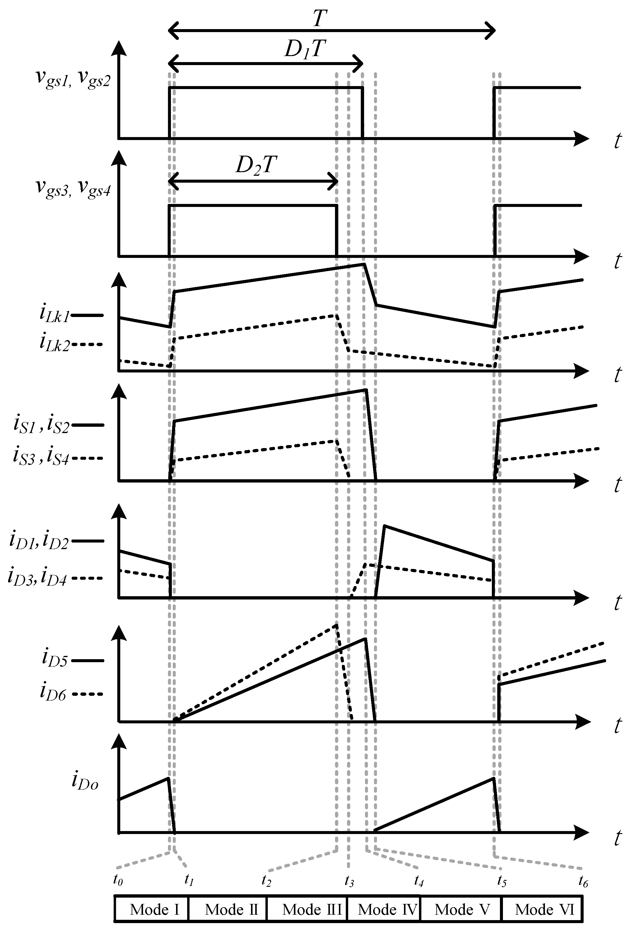
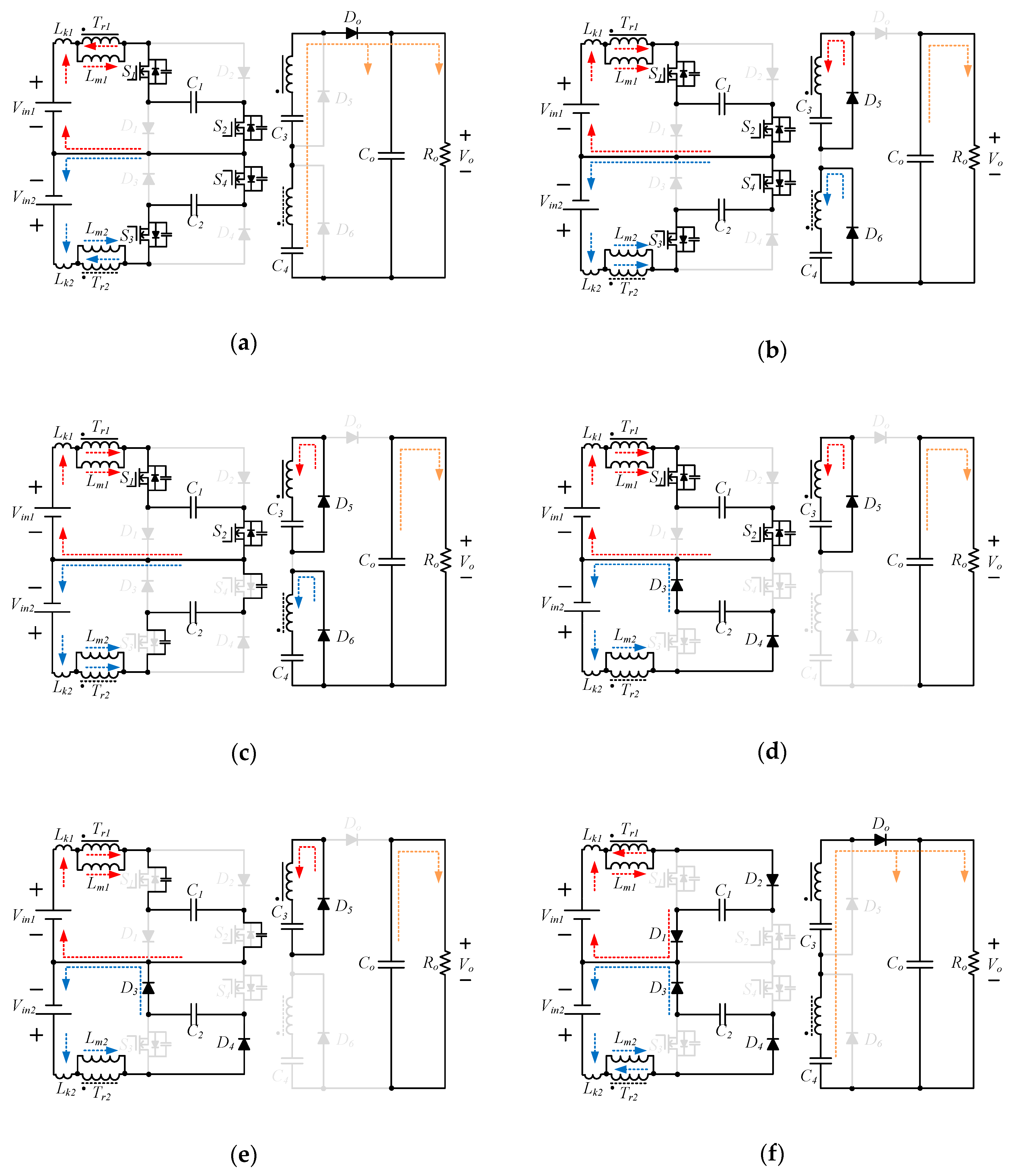
The switches S1 and S2 are turned on/off simultaneously, so do the switches S3 and S4. Assume that the turn-on period of S1 and S2 is D1Ts and D2Ts is for S3 and S4. In addition, the magnitude of Vin2 is twice that of Vin1. While the proposed DHSIC operates at DIO and in continuous conduction mode (CCM), converter operation over one switching cycle can be divided into six states. Converter operation will be described state by state as the following proceeds with. In addition, the equivalent of each state and conceptual waveforms are depicted in Figure 3 and Figure 4, respectively.
- State 1 [t0~t1]: Converter operation begins at this state, in which all switches S1–S4 are turned on at t = t0. All diodes are reverse except the output diode Do. The currents of leakage inductances, iLk1 and iLk2, increase linearly and steeply. Meanwhile, the energy stored in magnetizing inductances Lm1 and Lm2 is released to the output via transformers and diode Do. When leakage inductance current rises to be equal to magnetizing current, the diode current flowing through Do will drop to zero and then this state ends. The diode Do turns OFF under zero current transition. That is, the reverse-recovery problem at Do can be therefore overcome.
- State 2 [t1~t2]: In State 2, the switches S1–S4 remain ON. The diodes D1–D4 and Do are reversely biased, but diodes D5 and D6 are forwarded. In this time interval, leakage inductance and magnetizing inductance of the coupled inductor T1 absorb energy from Vin1 and C1, similarly, Lk2 and Lm2 of T2 from Vin1 and C1. The voltage across Tr1 is Vin1 + VC1 and Tr2 is Vin2 + VC2. At the secondary of the DHSIC, switched capacitors C3 and C4 are charged by the energy from coupled inductors Tr1 and Tr2, respectively. This state lasts for a time interval much longer than that of State 2 and is a major state in the converter operation.
- State 3 [t2~t3]: During the period from t2 to t3, switches S1 and S2 continue conducting. On the contrary, S3 and S4 are turned off at t2. The diodes D1–D4 and Do are reversely biased, but D5 and D6 are in a forward state. The parasitic capacitances of S3 and S4 are charged and current iLk2 decreases dramatically. As the increasing voltages blocked by S3 and S4 reach VC2, diodes D3 and D4 become forwarded and then the operation state enters State 4.
- State 4 [t3~t4]: All active switches remain the same on-off conditions as in State 3. That is, S1 and S2 are closed but S3 and S4 open. The voltage Vin1 + VC1 will supply Tr1 and forwards the energy to charge switched capacitor C3. Meanwhile, the capacitor C2 absorbs energy from Vin2 and Tr2. Leakage energy of Lk2 is recycled to C2. The voltage stress of S3 and S4 will be clamped to VC2. This operation state ends at the time both switches S1 and S2 are turned off.
- State 5 [t4~t5]: After S1 and S2 are turned off, the voltage across both switches increases. At the same time, their parasitic capacitances are charging toward the value of VC1. With respect to the other switches, S3 and S4 are still in the OFF state. Once parasitic capacitance-voltage approaches to VC1, State 5 ends and blocking voltage of S1 and S2 will be clamped at VC1. The switched capacitor C3 is still charging. During the time interval of State 5, the current flowing through Lk1 drops steeply. The diodes D1 and D2 will be forwarded at t = t5 and then this state ends.
- State 6 [t5~t6]: From t5 to t6, all switches remain OFF. The Lm1 pumps its stored energy to charge C1 and to the output as well. With respect to Lm2, it is also in energy-releasing but charges toward C2, meanwhile, part of its energy will be transformed to the secondary of Tr2 to power the output. The leakage energy stored in Tr1 and Tr2 will be recycled to capacitors C1 and C2, respectively. During State 6, the series voltage of Tr1, C3, Tr2, and C4 is connected to the output. That is, the output can accordingly obtain a high voltage level. Like State 2 and 4, State 6 also plays a major role in the converter operation. While switches S1–S4 are turned on again at t = t6, this state ends and converter operation over one switching cycle is completed.
2.2. Single-Input Operation
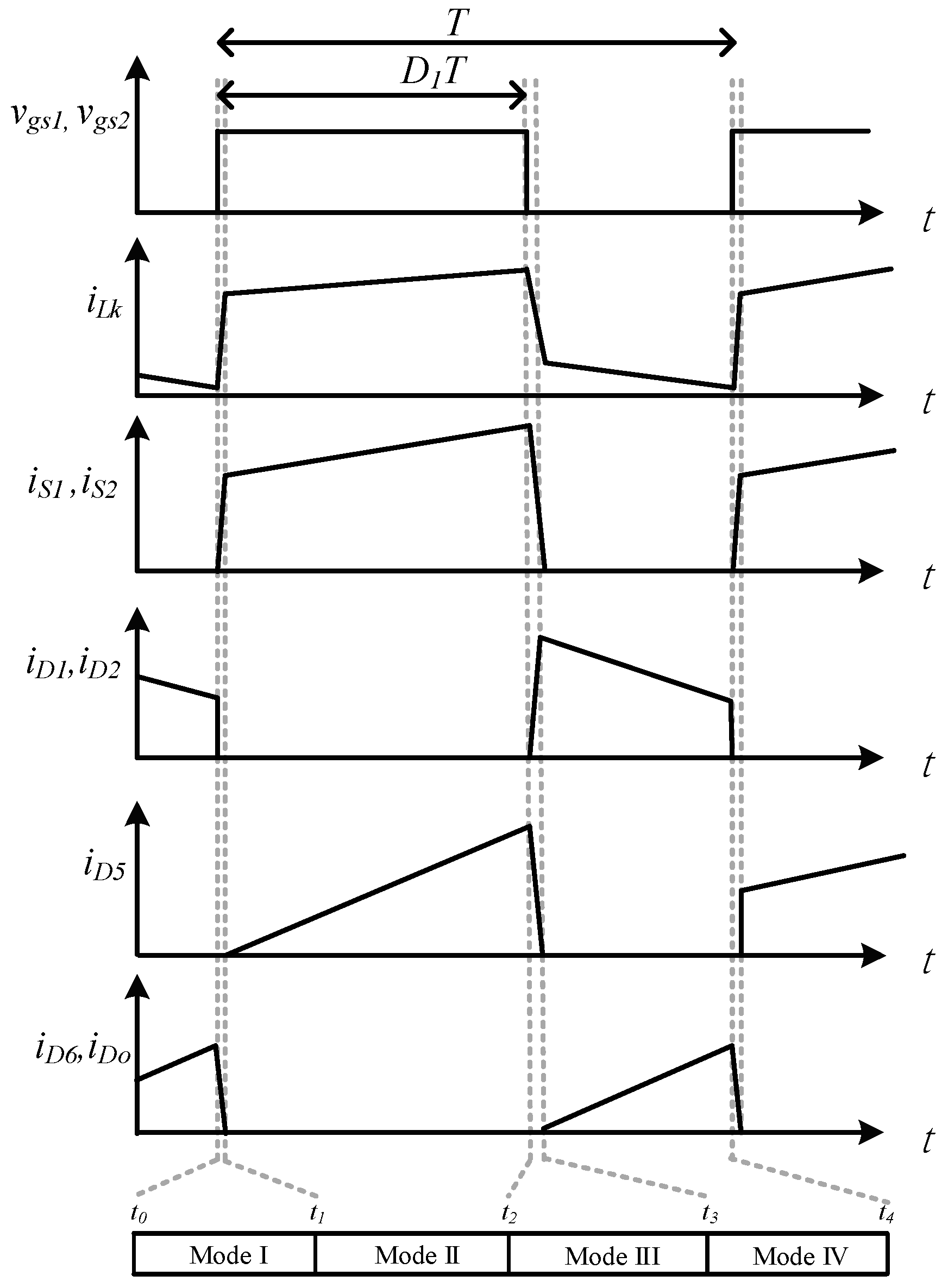
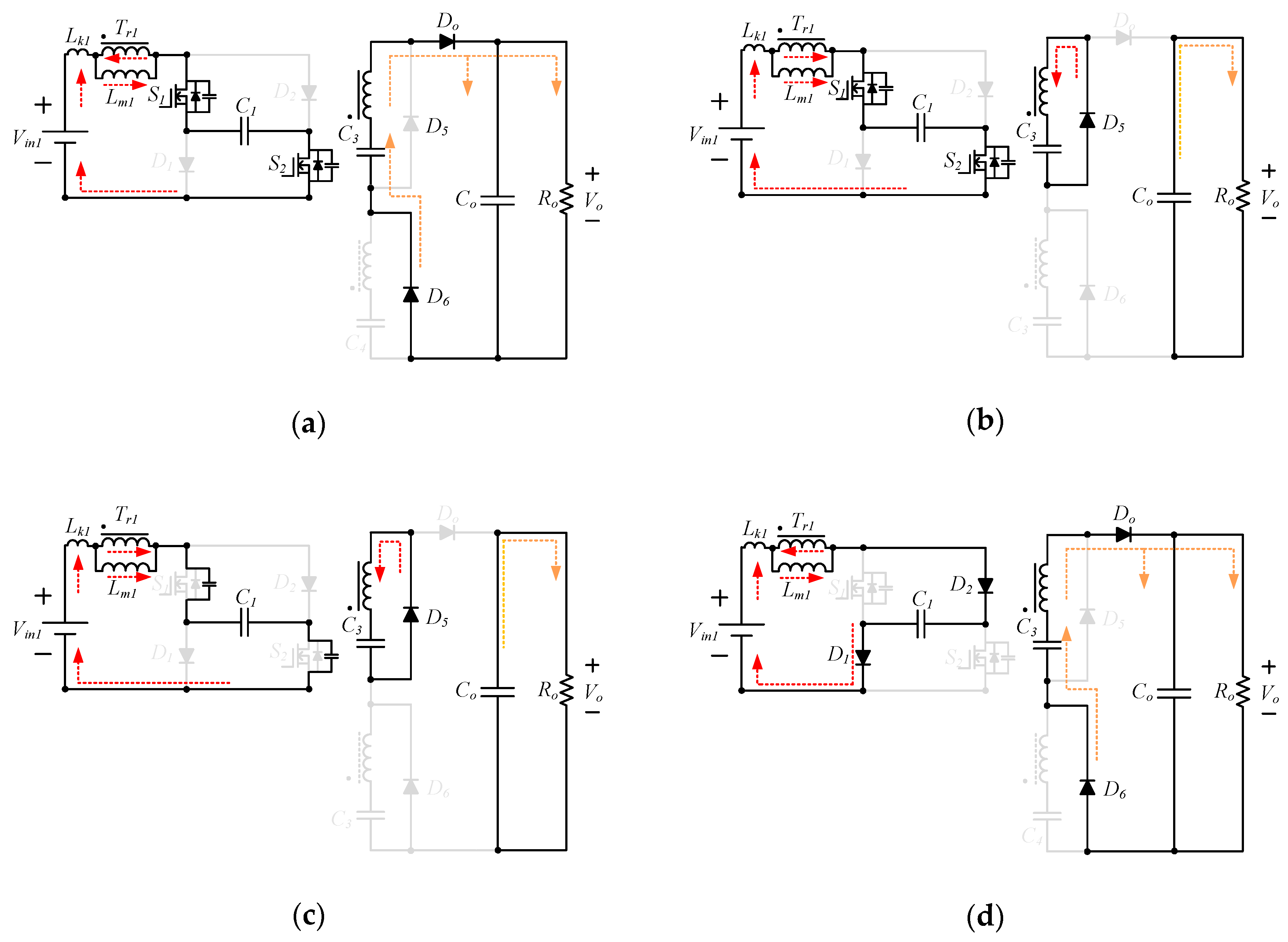
Once one of the inputs fails to supply power, the proposed converter still can function as a high step-up feature. Suppose that only Vin1 powers the DHSIC and in CCM condition. The converter will have four operation states over switching cycle. The corresponding key waveforms and equivalent circuits are illustrated in Figure 5 and Figure 6 in turn.
- State 1 [t0~t1]: If only Vin1 supplies the converter, power processing is controlled by switches S1 and S2. Both switches are turned on at t = t0 and converter operation begins. As shown in Figure 6a, the voltage across Tr1 will be equal to the series voltage of C1 and Vin1. Magnetizing inductance Lm1 pumps its stored energy to the secondary of Tr1. Therefore, the current flowing through Lm1 decreases. The current iLk1 increases quickly. When iLk1 is equal to iLm1, this state ends. At this time, the current flowing through the diodes Do and D6 also drops to zero. That is, the reverse-recovery problem of both diodes is therefore resolved.
- State 2 [t1~t2]: The equivalent of State 2 is illustrated in Figure 6b, in which the switches S1 and S2 remain closed. The Lm1 absorbs energy form Vin1 and C1 and thus iLm1 increases linearly. At the secondary of Tr1, the switched capacitor C3 is charging continuously over this stage. State 2 is a major state in the converter operation at SIO. At time t = t2, the switches S1 and S2 are turned off and then the converter operation enters the next stage.
- State 3 [t2~t3]: In State 2, all diodes are in reverse bias except D5. The parasitic capacitance of power switches S1 and S2 are charged and the current iLm1 decreases. The blocking voltage of S1 and S2 is therefore increasing. The associated equivalent is shown in Figure 6c. When the voltage across S1 and S2 approaches to VC1, diodes D1 and D2 become forwarded. Then, State 4 starts.
- State 4 [t3~t4]: The equivalent circuit refers to Figure 6d, in which the magnetizing inductance forwards its stored energy to charge capacitor C1 and to the output via the ideal transformer. Meanwhile, the leakage energy of Lk1 is recycled to C1, which also suppresses the voltage spike on the active switches. Over the time interval from t3 to t4, switches S1 and S2 are open. With respect to diode, the D5 is in reverse state but D1, D2, D6 and Do are forward biased. State 4 is also a major state similar to State 2, dominating the converter operation. Both switches S1 and S2 will be turned on again at t = t4 and then this state ends. Converter operation over one switching cycle is completed.
3. Steady-State Analysis of Proposed Converter
The voltage ratio of output to input, voltage stress and current stress of the semiconductor device, and magnetizing inductance design will be covered in this section. To simplify the steady-state analysis, the following assumptions are made.
- The values of the boosting capacitors C1 and C2 are large enough so as to keep their across voltages invariant.
- All diodes are regarded to be ideal. That is, forward drop voltage and ON-state resistance are neglected.
- The magnetizing inductance of the coupled inductor is much more than leakage inductance so that influence of the leakage inductance can be ignored.
- The turns ratios of the coupled inductors, N1s/N1p and N2s/N2p, are defined as n1 and n2, respectively.
- The DHSIC is at CCM operation.
The driving pattern relating to the four switches is the same as that discussed in the previous section. The S1 and S2 are closed for D1T and S3 and S4 for D2T. In addition, the duty ratio of D1 is greater than D2. Based on the assumptions made at the beginning of this section, states 2, 4 and 6 in Figure 4 will dominate the converter operation.
3.1. Voltage Conversion Ratio
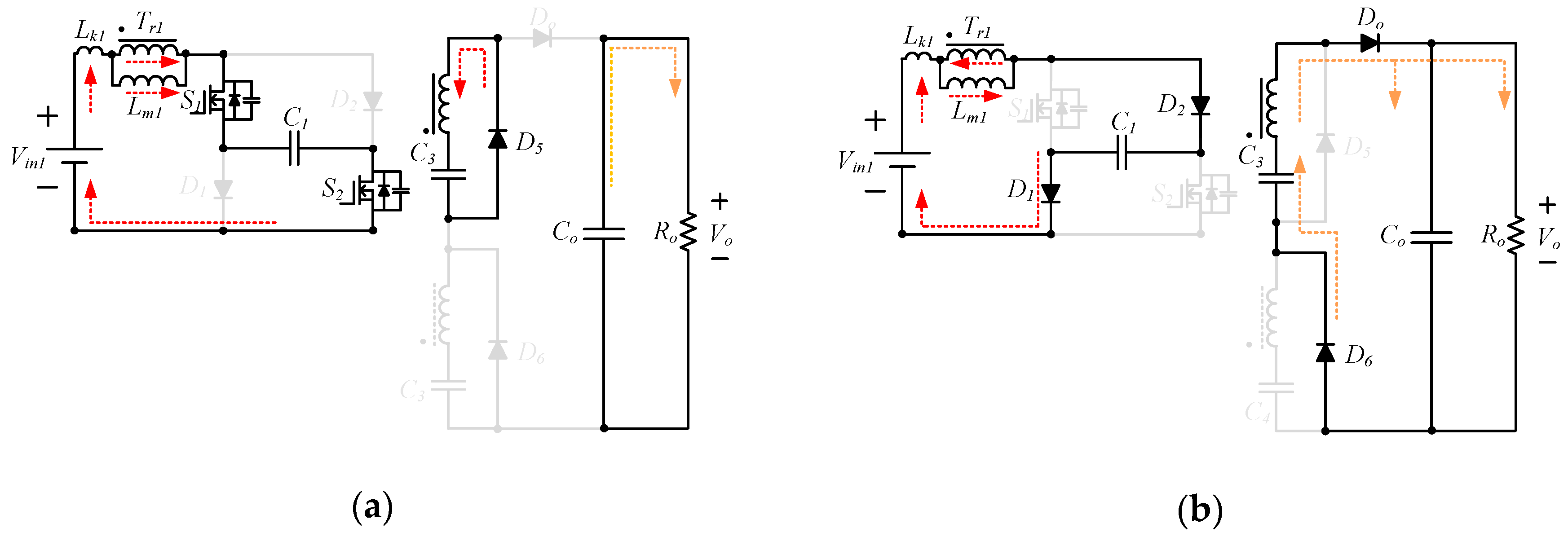
The proposed DHSIC can be regarded as a combination of two step-up converters which are symmetrical to common ground at the input side and in series connection at the output port. Furthermore, the two step-up converters are capable of operating individually. Therefore, the obtaining of voltage conversion ratio of the DHSIC can simply be derived from a single input situation and then to augment to dual-input situation. Suppose that only the Vin1 powers the DIC and both switches S1 and S2 are closed for D1T and open for (1 − D1)T over one switching period. The equivalents of switch ON and OFF are depicted in Figure 7. Applying voltage second balance criterion to Lm1 can yield
From Figure 7b, the VLm1,on and VLm1,off can be obtained as follows:
and
Substituting Equations (2) and (3) into Equation (1) can find the expression of VC1:
From Figure 7a, the voltage across capacitor C3, VC3, is found by the multiplication of turns ratio n1 and VLm1,on, and then, from Equations (2) and (4) the VC3 can be written as
According to Figure 7b, the following relationship holds:
Based on Equations (3)–(6), the output voltage of the converter at SIO can be given by
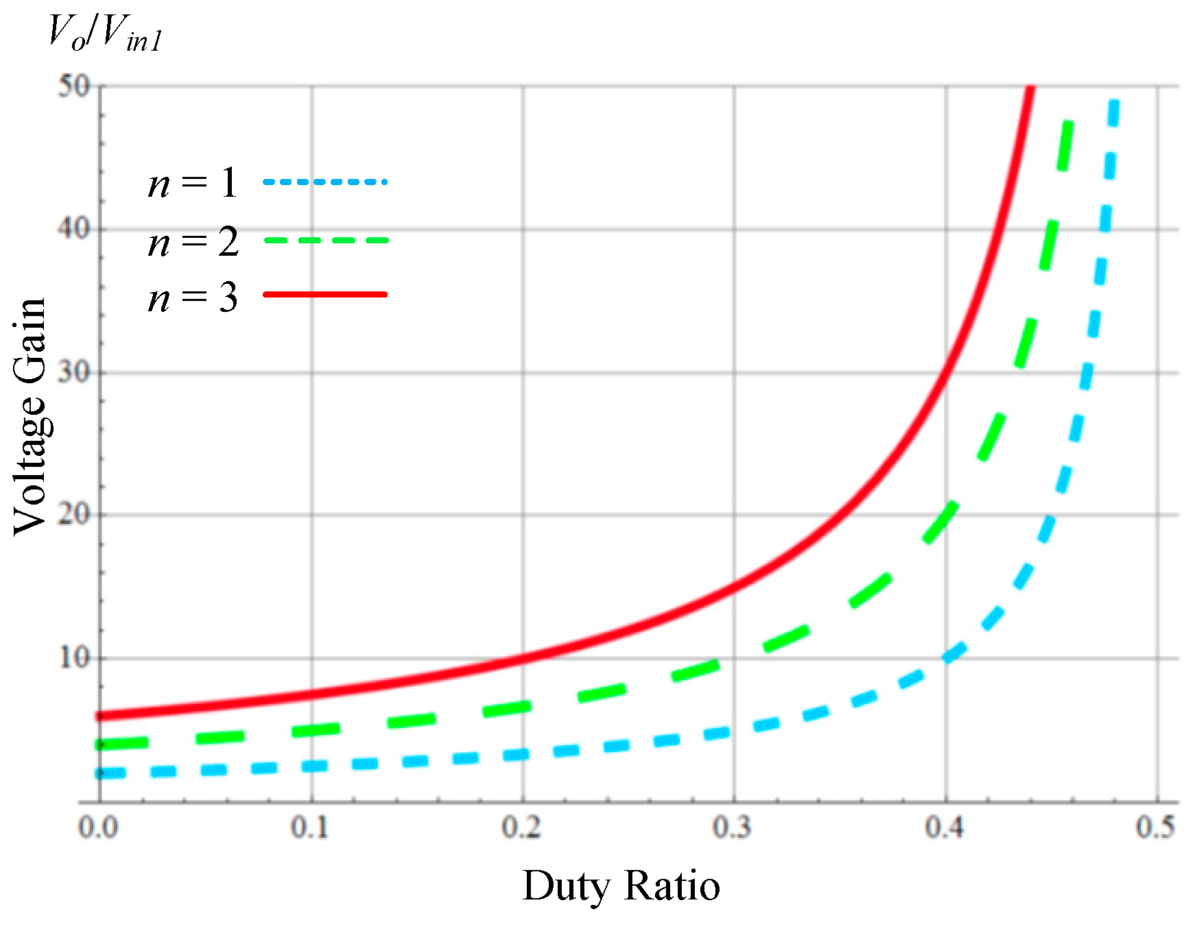
According to Equation (7), the switch duty ratio has to be less than 0.5, which is the converter limitation. Figure 8 depicts the relationship of voltage gain and duty ratio under different turns ratio.
With respect to the DIO situation, the DHSIC has the same control scheme shown in Figure 3. The S1 and S2 are closed for D1T and open for (1 − D1)T, while S3 and S4 are closed for D2T and open for (1−D2)T over one switching period. Equations (4) and (5) can be applied to the finding for the voltages of C2 and C4. That is, VC2 and VC4 are calculated by
and
respectively. Being similar to Equation (6), the following relationship will hold under a dual-input situation.
Thus, the corresponding output voltage at DIO of the converter can be described as
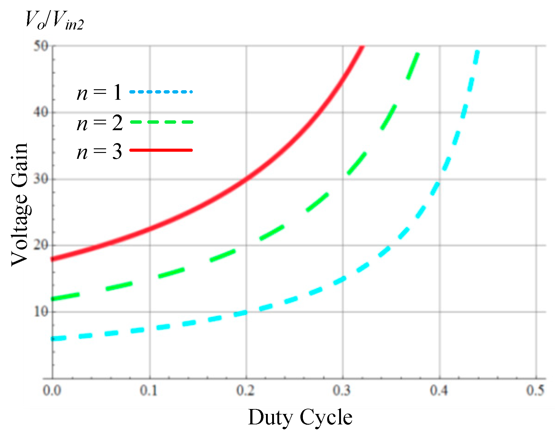
Assume that Vin2 = 2Vin1, D1 = D2 = D, and n1 = n2 = n, according to Equation (11), Figure 9 represents the relationship of voltage gain versus turns ratio, while under DIO situation.
3.2. Voltage Stress of Semiconductor Device
According to the structure of the DHSIC, the semiconductor devices, S1, S2, D1, and D2, will have the same voltage stress. In addition, the power stage has inherently symmetrical configuration and is able to operate independently and individually at primary side. Therefore, the voltage stress of S1, S2, D1, and D2 can be determined from Figure 7, accordingly all of which will be equal to VC1. From Equation (4), this voltage stress is expressed as
Similarly, voltage stress of S3, S4, D3, and D4 can be determined by
With attention to the semiconductor devices at the output port (the secondary side of the DHSIC), an associated determination is discussed in the following. While all active switches are in OFF-state, the blocking voltages of diodes D5 and D6 are obtained by
and
respectively. The VC1 and VC3 can be founded by Equations (4) and (5) in turn, and VC2 and VC4 by Equations (8) and (9). As a result, the above Equations (14) and (15) can be rewritten as
and
respectively. Voltage stress of the output diode DO is estimated at the state that all active switches are closed and thus it will be
Based on Equations (4), (5), (8) and (9), the expression of Equation (18) is rewritten as
3.3. Magnetizing Inductance Design
The minimum currents of active switches S1 and S2, iLm1,min and iLm2,min, can be expressed as
and
respectively. The ΔiLm1 and ΔiLm2 stand for the current change on Lm1 and Lm2 in turn, while ILm1 and ILm2 are the average currents of Lm1 and Lm2. Assume that the converter is lossless. Then, The ILm1 and ILm2 can be determined as follows:
and
in which the Io denotes output current. In addition, ΔiLm1 and ΔiLm2 can be calculated by
and
At the boundary, ΔiLm1 and ΔiLm2 are equal to zero, that is,
and
From Equations (26) and (27), the minimum magnetizing inductances for CCM operation have to meet the following inequality:
and
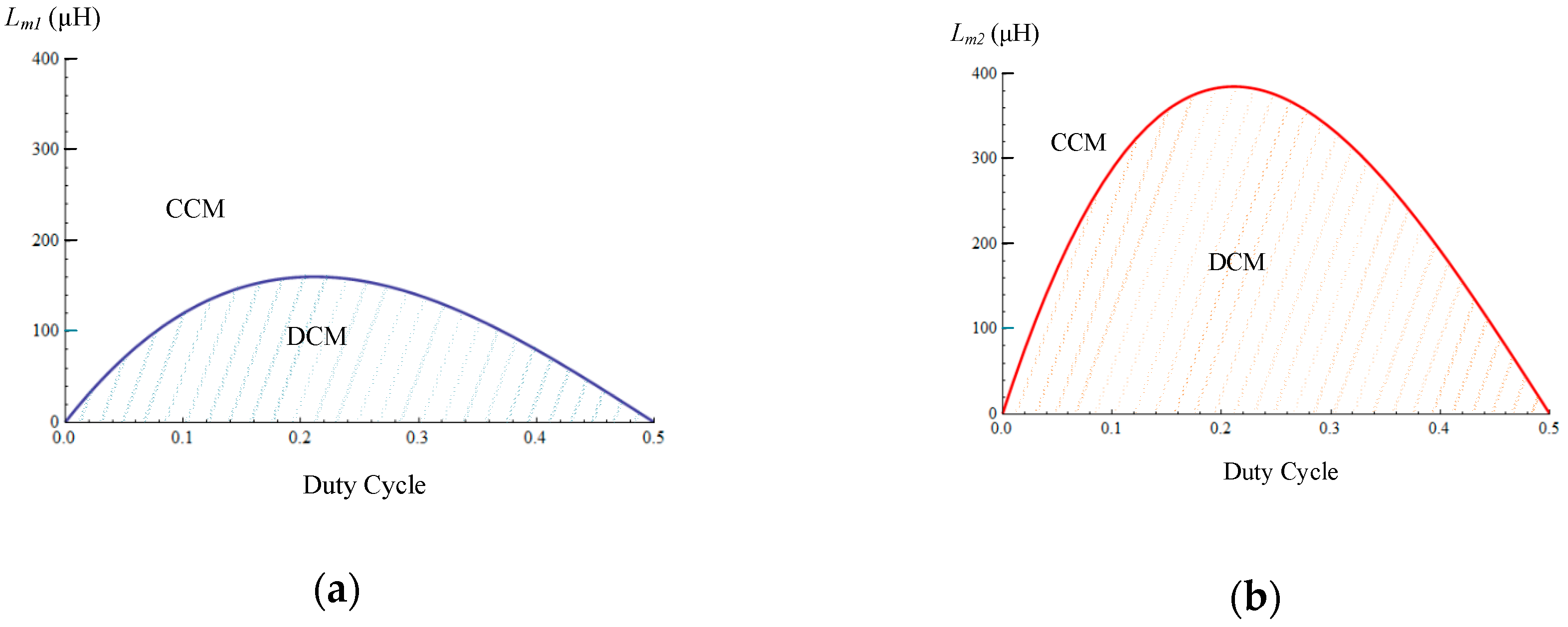
Suppose that the turns ratio n1 = n2 = n, Vin2 = 2Vin1 = 24 V, switching frequency fs = 40 kHz, and both switches have the same duty ratio denoted as D. In addition, the converter operates at boundary condition mode (BCM) at 25 W. Figure 10 illustrates the relationship between magnetizing inductance and duty ratio for Lm1 and Lm2.
The comparison with other similar converters is summarized in Table 1. It can be found that even though the DHSIC needs more power components, it achieves excellent voltage gain over other DICs in addition to that the features of galvanic isolation, continuous input current and switch voltage clamping still can be possessed.
4. Experimental Results
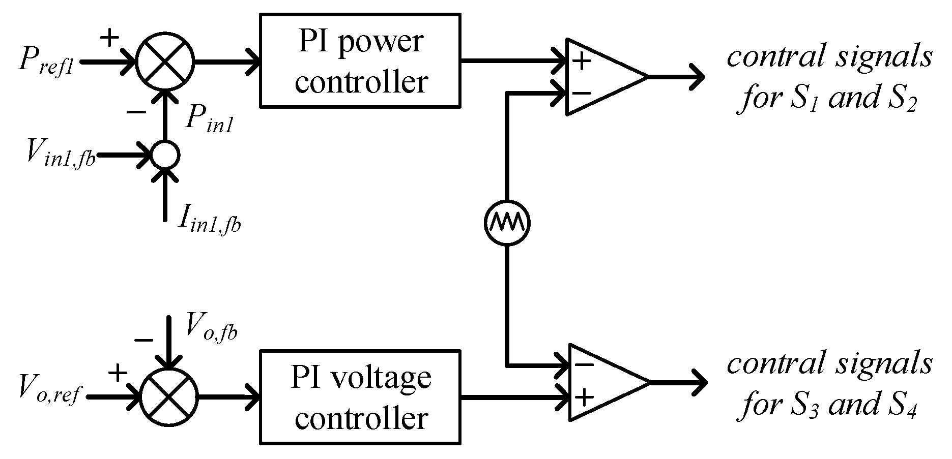
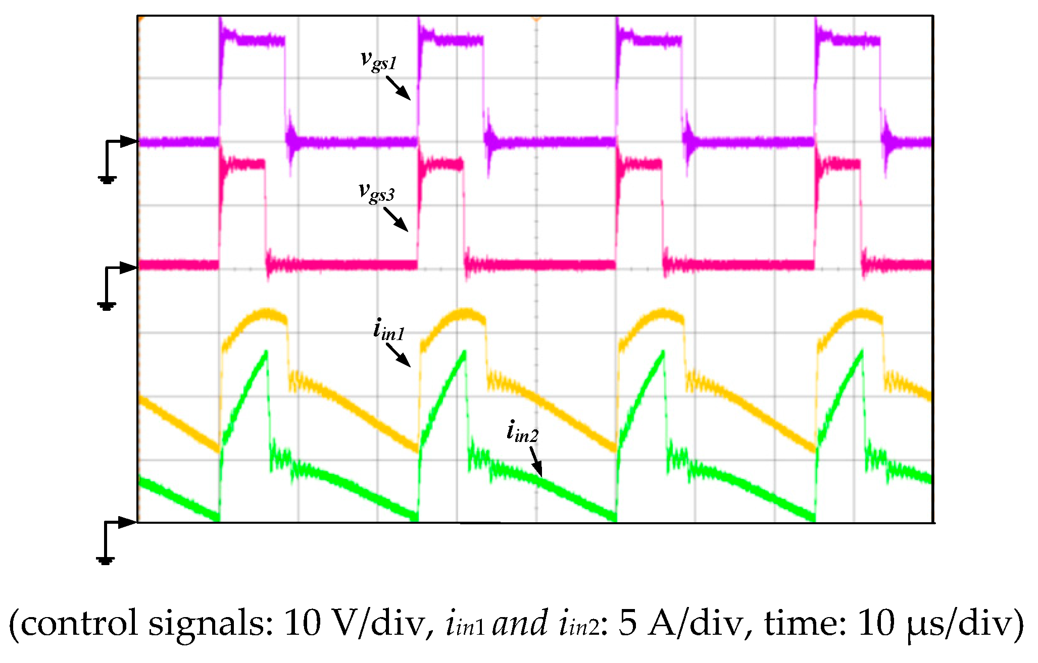
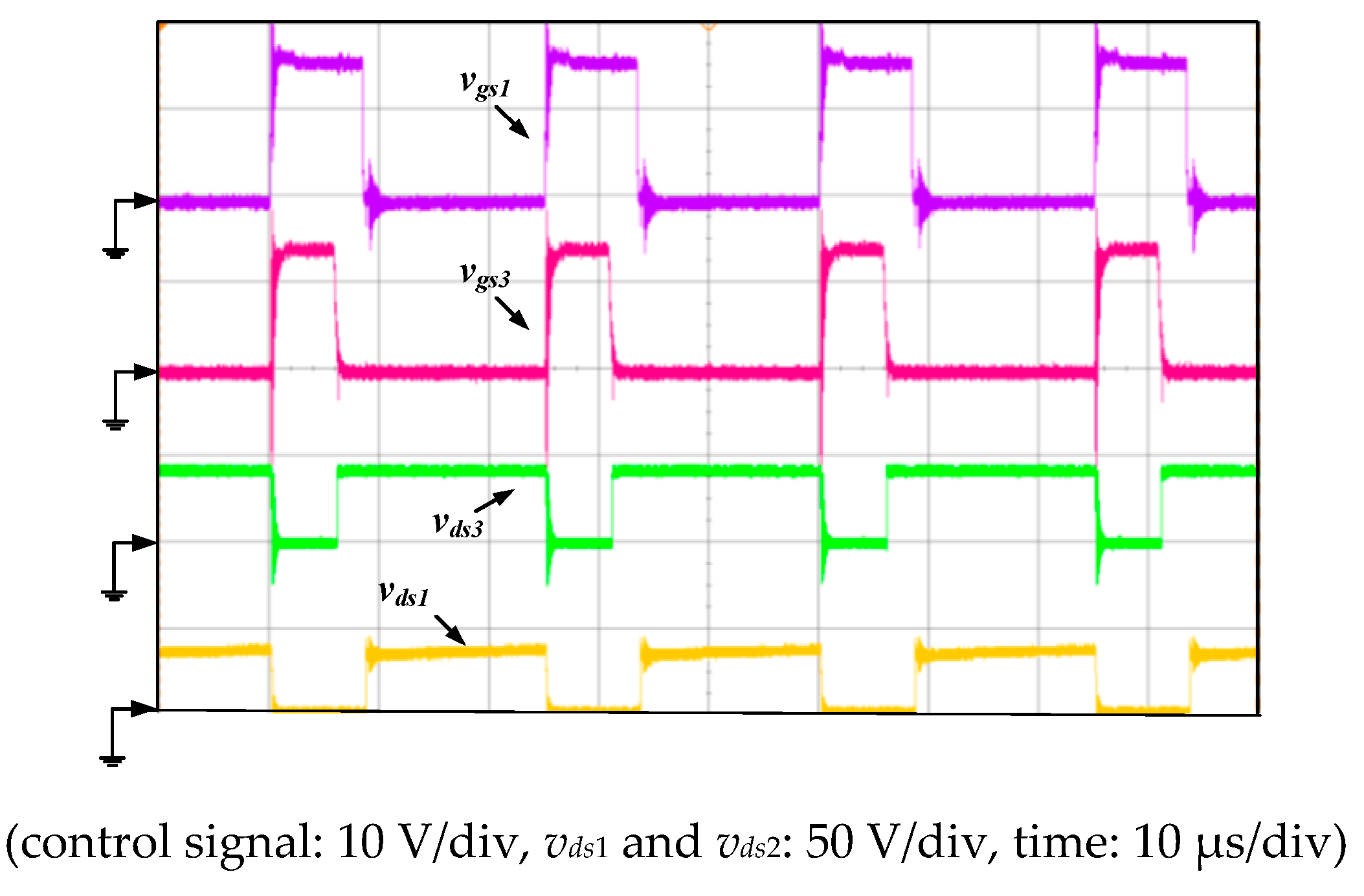
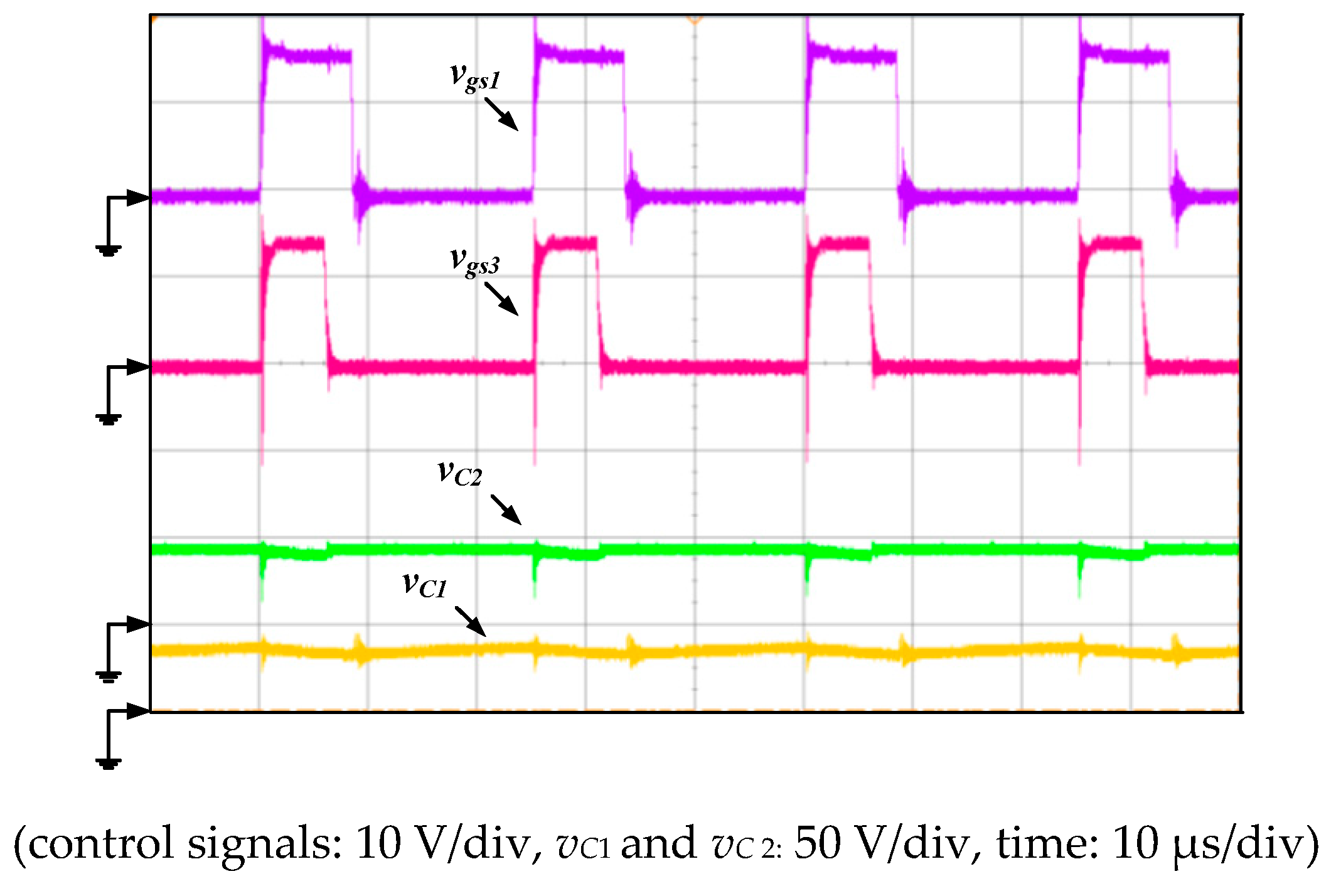
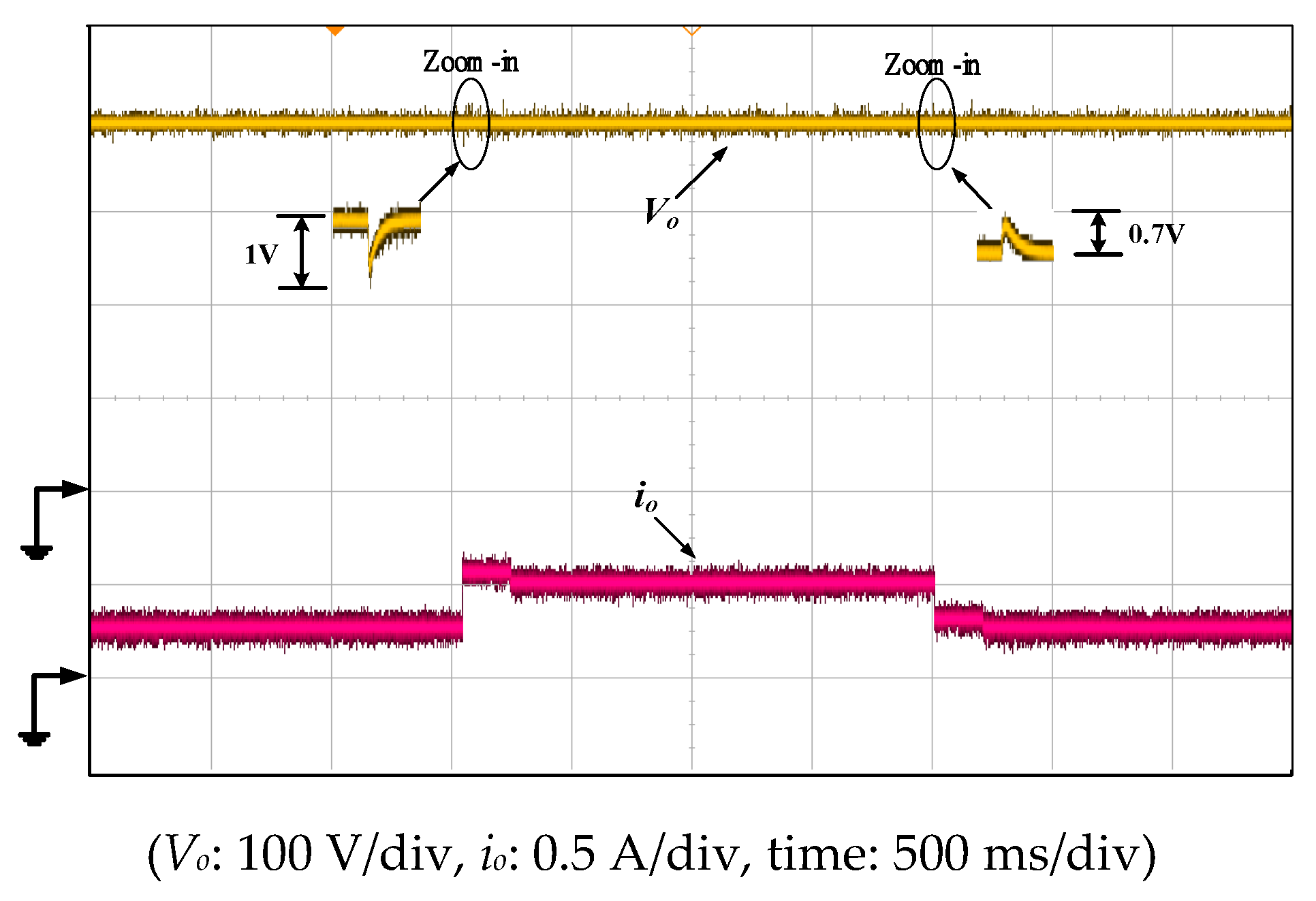
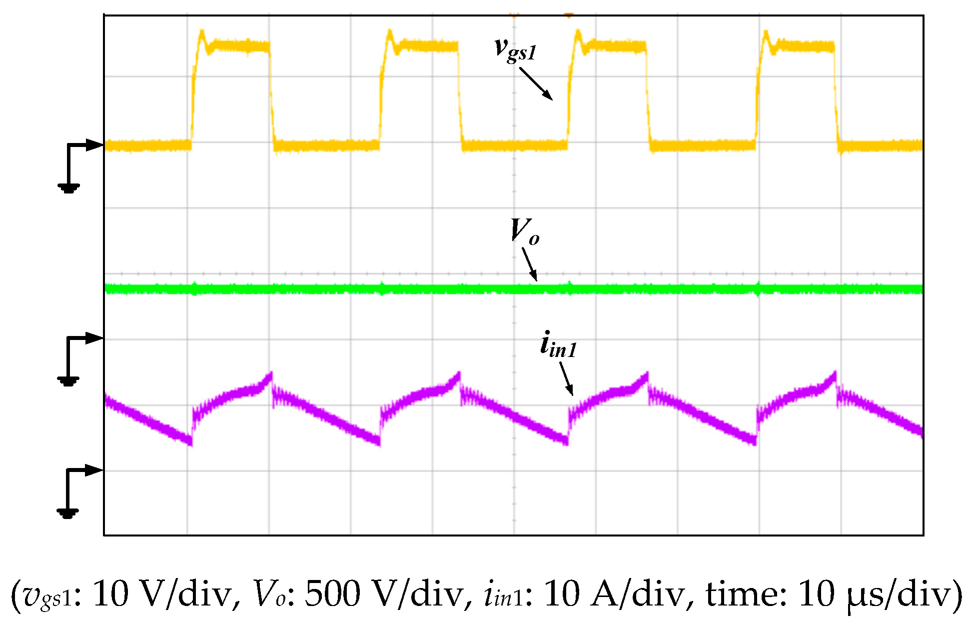
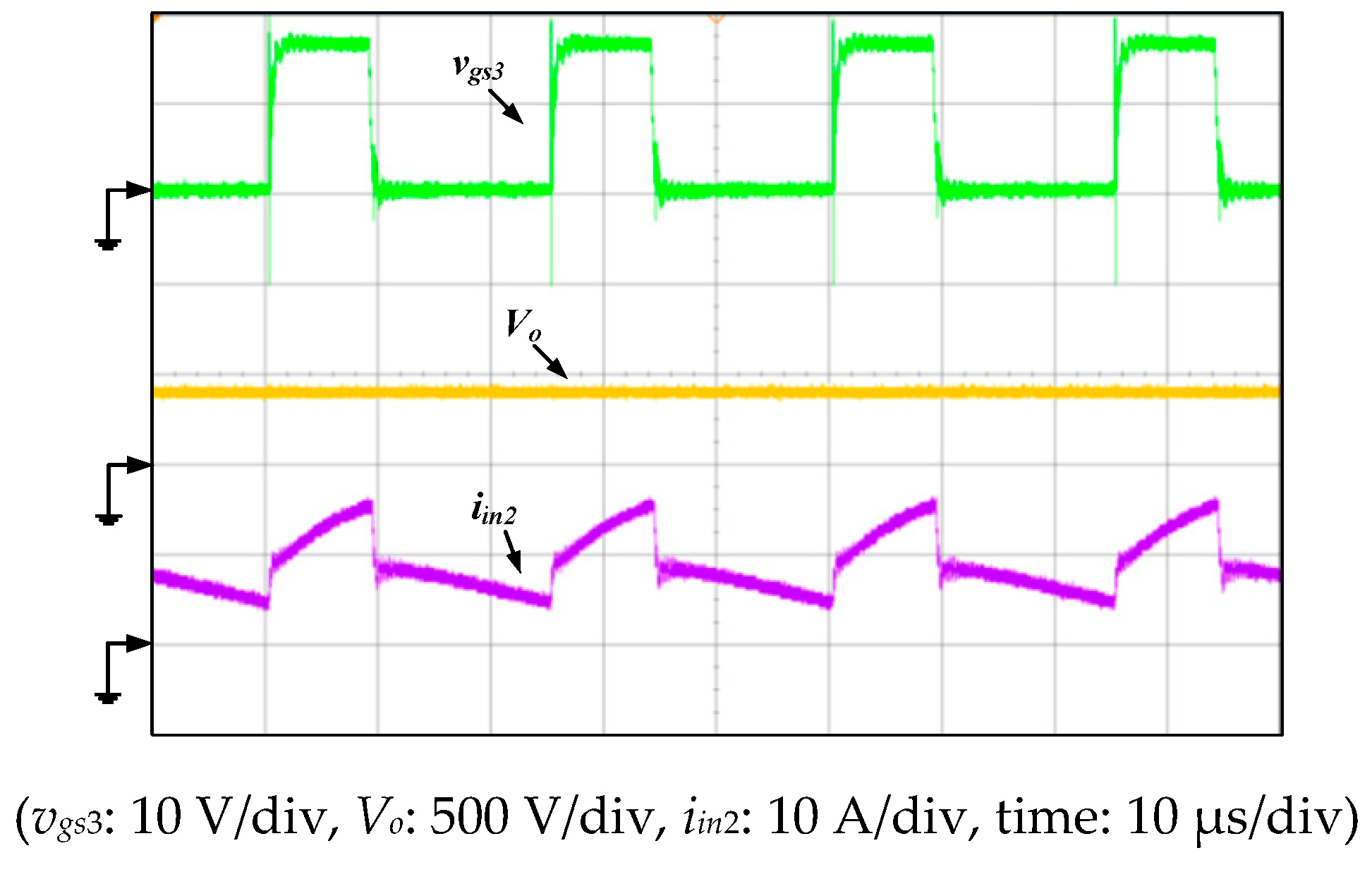
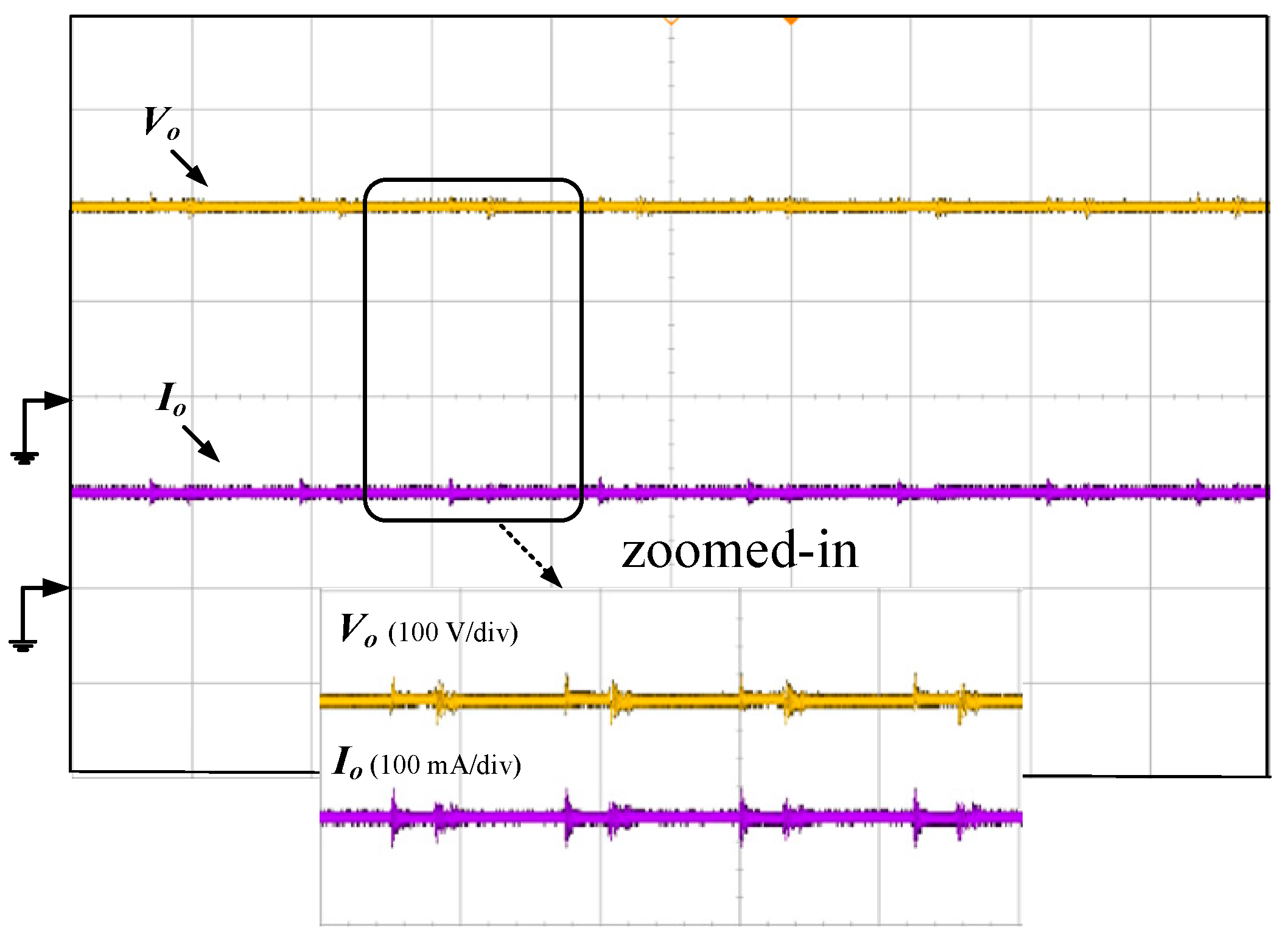
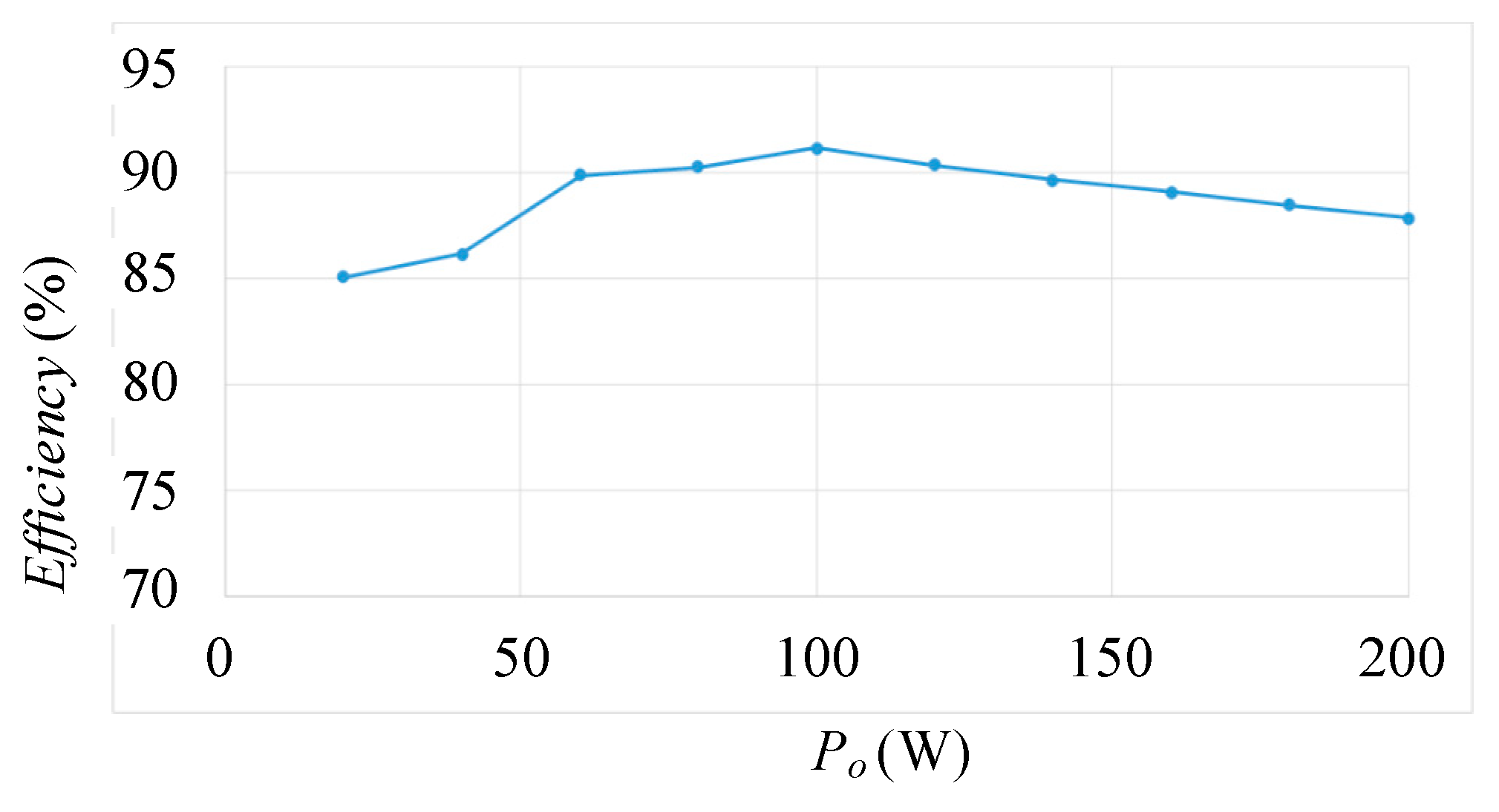
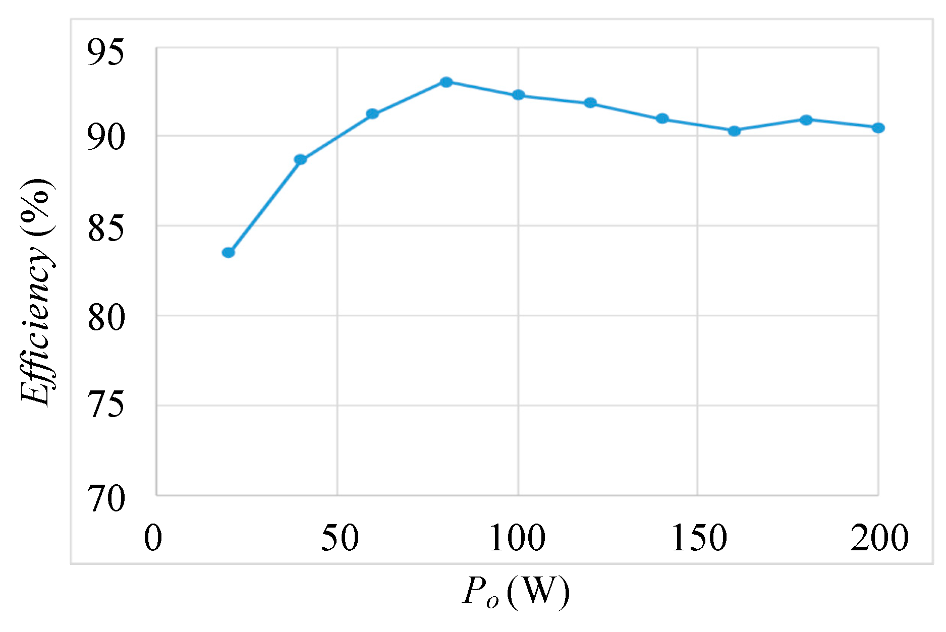
To verify the proposed DIC, a 200-W prototype is built, simulated and measured. Converter parameters and components adopted are summarized in Table 2. The control block diagram of the prototype is depicted in Figure 11. Power of input port 1 is calculated according to the detected input voltage and current, that is, Vin1,fb, and Iin1,fb, and then it is compared to a reference Pref1. The control signals for S1 and S2 are determined by the PI power controller and the carrier. Accordingly, the input power at port 1 can be readily controlled. With respect to the other part of the control block diagram, the output voltage is regulated by controlling the switches S3 and S4. With such voltage regulation, the input port 2 can accommodate the supplement to output power and thus power dispatch at both input ports is accomplished. The proposed converter adopts MCU dsPIC30F4011 to serve as system controller. Figure 12 shows the control signals and the corresponding input currents at full load under DIO situation. In Figure 12 the duty ratios of S1 and S2 are 0.32 and 0.23, respectively, which is consistent with Equation (11) for a 400-V output. Meanwhile, the switch voltages, vds1 and vds2, are measured and shown in Figure 13, from which it can be observed that there is no voltage spike on active switches. That is, the boosting capacitors C1 and C2 are able to recycle leakage energy and can effectively clamp switch voltage. Additionally, withstood voltages on the switches at port 1 and port 2 are 34 V and 45 V, respectively, which verifies the theoretical analysis results of Equations (12) and (13). Figure 14 is the measurement of the voltages of boosting capacitors. This figure reveals that voltages of C1 and C2 are in turn 34 V and 45 V, both voltage magnitudes of which meet the theoretical results of Equations (4) and (8). While step change takes place from half load to full load and then drops back, Figure 15 shows the related output voltage and current. Figure 15 illustrates that constant 400-V output still can be kept with even under step change. The overshoots at step-up and step-down transitions are only 1 V and 0.7 V, respectively. With respect to SIO situation, once power failure occurs at input 1, Figure 16 shows the measured control signal, output voltage, and input current. Similarly, if at input 2, Figure 17 is the related measurement. Both figures demonstrate the operation ability of the converter at SIO situation. The measured waveform of output current is presented in Figure 18, from which it can be observed that the output current of the converter is near to be ripple-free. The efficiency of the proposed converter is measured and then shown in Figure 19, in which the peak value is about 91.4%. In the experiment, a very low level of voltage, Vin1 = 12 V, is considered, therefore, which yields that higher current has to be demanded at a specific power, resulting in large conduction loss. This is the major reason why the converter efficiency is not as high as satisfied in the measurement. However, if input voltage is raised, the converter efficiency will be advanced. At single-input situation, if only the 24 V of Vin2 suppled the DHSIC, measured converter efficiency is shown in Figure 20. This figure reveals that a higher voltage input can yield a better efficiency even under the operation of single input. A photo of the built-up DHSIC is shown in Figure 21.
5. Conclusions
In this paper, a dual-input converter is proposed, which possesses the characteristics of ultra-high voltage gain, continuous input currents, galvanic isolation, inherent voltage-clamp feature, and recycling the energy stored in leakage inductance. This converter is capable of controlling the dual inputs independently and individually. Moreover, it still can accomplish all the mentioned features even under the case that either input encounters power failure. That is, the converter has operation flexibility to operate at dual-input situation or single-input situation for accommodating input conditions. A maximum of measured efficient is about 91.4% at dual-input operation.
Author Contributions
Conceptualization, C.-L.S., L.-Z.C. and H.-Y.C.; writing-original draft preparation, C.-L.S. and L.-Z.C.; writing-review and editing, C.-L.S. and L.-Z.C.; methodology, C.-L.S., L.-Z.C. and H.-Y.C.; validation, C.-L.S. and L.-Z.C.; supervision, C.-L.S.
Funding
This research received no external funding.
Conflicts of Interest
The authors declare no conflict of interest.
References
- Wang, Z.; Li, H. Integrated MPPT and Bidirectional Battery Charge for PV Application Using One Multiphase Interleaved Three-Port DC-DC Converter. In Proceedings of the Applied Power Electronics Conference and Exposition (APEC 2011), Fort Worth, TX, USA, 6–11 March 2011; pp. 295–300. [Google Scholar]
- Williams, M.C. Fuel Cells and the World Energy Future. In Proceedings of the Power Engineering Society Summer Meeting, Vancouver, BC, Canada, 15–19 July 2001; p. 725. [Google Scholar]
- Bryant, B.; Kazimierczuk, M.K. Voltage-Loop Power Stage Transfer Functions with MOSFET Delay for Boost PWM Converter Operating in CCM. IEEE Trans. Ind. Electron. 2007, 54, 347–353. [Google Scholar] [CrossRef]
- Medina-Garcia, A.; Schlenk, M.; Morales, D.P.; Rodriguez, N. Resonant Hybrid Flyback, a New Topology for High Density Power Adaptors. Electronics 2018, 7, 363. [Google Scholar] [CrossRef]
- Lin, B.R.; Hsieh, F.Y. Soft-Switching Zeta-Flyback Converter with a Buck-Boost Type of Active Clamp. IEEE Trans. Ind. Electron. 2007, 54, 2813–2822. [Google Scholar]
- Wang, C.M. A Novel ZCS-PWM Flyback Converter with a Simple ZCS-PWM Commutation Cell. IEEE Trans. Ind. Electron. 2008, 55, 749–757. [Google Scholar] [CrossRef]
- Almalaq, Y.; Matin, M. Three Topologies of a Non-Isolated High Gain Switched-Inductor Switched-Capacitor Step-Up Cuk Converter for Renewable Energy Applications. Electronics 2018, 7, 94. [Google Scholar] [CrossRef]
- Shu, L.J.; Liang, T.J.; Yang, L.S.; Lin, R.L. Transformerless High Step-Up DC-DC Converter Using Cascode Technique. In Proceedings of the Power Electronics Conference, Sapporo, Japan, 21–24 June 2010; pp. 63–67. [Google Scholar]
- Young, C.M.; Chen, M.H.; Chang, T.A.; Ko, C.C. Transformerless High Step-Up DC-DC Converter with Cockcroft-Walton Voltage Multiplier. In Proceedings of the 2011 6th IEEE Conference on Industrial Electronics and Applications, Beijing, China, 21–23 June 2011; pp. 1599–1604. [Google Scholar]
- Axelorod, B.; Berkovic, Y.; Ioinovici, A. Switched-Capacitor/Switched-Inductor Structures for Getting Transformerless Hybrid DC-DC PWM Converters. IEEE Trans. Circuits Syst. I. 2008, 55, 687–696. [Google Scholar] [CrossRef]
- Changchien, S.K.; Liang, T.J.; Chen, J.F.; Yang, L.S. Novel high step-up dc-dc converter for fuel cell energy conversion system. IEEE Trans. Ind. Electron. 2010, 57, 2007–2017. [Google Scholar] [CrossRef]
- Chen, S.M.; Liang, T.J.; Yang, L.S.; Chen, J.F. A Cascade high step-up dc-dc converter with single switch for microsource application. IEEE Trans. Power Electron. 2011, 26, 1146–1153. [Google Scholar] [CrossRef]
- Hsieh, Y.P.; Chen, J.F.; Liang, T.J.; Yang, L.S. Novel high step-up dc-dc converter with coupled-inductor and switched –capacitor technique for a sustainable energy system. IEEE Trans. Power Electron. 2011, 26, 3481–3490. [Google Scholar] [CrossRef]
- Cheng, X.-F.; Zhang, Y.; Yin, C. A ZVS Bidirectional Inverting Buck-Boost Converter Using Coupled Inductors. Electronics 2018, 7, 221. [Google Scholar] [CrossRef]
- Hou, S.; Chen, J.; Sun, T.; Bi, X. Multi-input Step-Up Converters Based on the Switched-Diode-Capacitor Voltage Accumulator. IEEE Trans. Power Electron. 2016, 31, 381–393. [Google Scholar] [CrossRef]
- Liu, F.; Wang, Z.; Mao, Y.; Ruan, X. Asymmetrical Half-Bridge Double-Input DC/DC Converters Adopting Pulsating Voltage Source Cells for Low Power Applications. IEEE Trans. Power Electron. 2014, 29, 4741–4751. [Google Scholar] [CrossRef]
- Benavides, N.D.; Chapman, P.L. Power Budgeting of A Multiple-Input Buck-Boost Converter. IEEE Trans. Power Electron. 2005, 20, 1303–1309. [Google Scholar] [CrossRef]
- Reddi, N.K.; Ramteke, M.R.; Suryawanshi, H.M. Dual-Input Single-Output Isolated Resonant Converter with Zero Voltage Switching. Electronics 2018, 7, 96. [Google Scholar] [CrossRef]
- Babaei, E.; Abbasi, O. Structure for multi-input multi-output dc–dc boost converter. IET Power Electron. 2016, 9, 9–19. [Google Scholar] [CrossRef]
- Matsuo, H.; Shigemizu, T.; Kurokawa, F.; Watanable, N. Characteristics of the Multiple-Input DC-DC Converter. In Proceedings of the Power Electronics Specialists Conference, Seattle, WA, USA, 20–24 June 1993; pp. 115–120. [Google Scholar]
- Kobayashi, K.; Matsuo, H.; Sekine, Y. Novel Solar-Cell Power Supply System Using A Multiple-Input DC-DC Converter. IEEE Trans. Ind. Electron. 2006, 53, 281–286. [Google Scholar] [CrossRef]
- Matsuo, H.; Lin, W.; Kurokawa, F.; Shigemizu, T.; Watanable, N. Characteristics of the Multiple-Input DC-DC Converter. IEEE Trans. Ind. Electron. 2004, 51, 625–631. [Google Scholar] [CrossRef]
- Chen, Y.M.; Liu, Y.C.; Lin, S.H. Double-Input PWM DC-DC Converter for High/Low Voltage Sources. In Proceedings of the Telecommunications Energy Conference, Yokohama, Japan, 23 October 2003; pp. 27–32. [Google Scholar]
- Danyali, S.; Hosseini, S.H.; Gharehpetian, G.B. New Extendable Single-Stage Multi-input DC–DC/AC Boost Converter. IEEE Trans. Power Electron. 2014, 29, 775–788. [Google Scholar] [CrossRef]
Figure 1.
An illustration of the hybrid renewable-energy generation system.

Figure 2.
Equivalent circuit of the proposed converter.

Figure 3.
The conceptual key waveform of the proposed converter at DIO (dual input operation) and CCM (continuous conduction mode) operation.
Figure 3.
The conceptual key waveform of the proposed converter at DIO (dual input operation) and CCM (continuous conduction mode) operation.

Figure 4.
The equivalents of the proposed converter at DIO and CCM operation: (a) State 1, (b) State 2, (c) State 3, (d) State 4, (e) State 5, (f) State 6.
Figure 4.
The equivalents of the proposed converter at DIO and CCM operation: (a) State 1, (b) State 2, (c) State 3, (d) State 4, (e) State 5, (f) State 6.

Figure 5.
Conceptual key waveform of the proposed converter at SIO (single-input operation) and CCM operation.
Figure 5.
Conceptual key waveform of the proposed converter at SIO (single-input operation) and CCM operation.

Figure 6.
The equivalents of the proposed converter at SIO and CCM operation: (a) State 1, (b) State 2, (c) State 3, (d) State 4.
Figure 6.
The equivalents of the proposed converter at SIO and CCM operation: (a) State 1, (b) State 2, (c) State 3, (d) State 4.

Figure 7.
The simplified equivalents while DHSIC (dual-input high step-up isolated converter) operates at SIO: during (a) switch-ON interval, (b) switch-OFF interval.
Figure 7.
The simplified equivalents while DHSIC (dual-input high step-up isolated converter) operates at SIO: during (a) switch-ON interval, (b) switch-OFF interval.

Figure 8.
The voltage gain versus duty ratio under the SIO situation.

Figure 9.
The voltage gain versus duty ratio under the DIO situation.

Figure 10.
The relationship between the magnetizing inductance and the duty cycle. (a) Lm1, (b) Lm2.
Figure 10.
The relationship between the magnetizing inductance and the duty cycle. (a) Lm1, (b) Lm2.

Figure 11.
Control block diagram of the proposed converter.

Figure 12.
The waveforms of control signals and corresponding input currents at full load under the DIO situation.
Figure 12.
The waveforms of control signals and corresponding input currents at full load under the DIO situation.

Figure 13.
The practical waveforms of the voltages across active switches.

Figure 14.
The voltage measurement of boosting capacitors C1 and C2.

Figure 15.
The waveforms of output voltage and current while step change occurs at load.

Figure 16.
The measured waveforms of the control signal, output voltage, and input current while input 2 encounters power failure.
Figure 16.
The measured waveforms of the control signal, output voltage, and input current while input 2 encounters power failure.

Figure 17.
The measured waveforms of the control signal, output voltage, and input current while input 1 encounters power failure.
Figure 17.
The measured waveforms of the control signal, output voltage, and input current while input 1 encounters power failure.

Figure 18.
The practical measurement of output current Io.

Figure 19.
The conversion efficiency of the proposed converter.

Figure 20.
Measured converter efficiency while only input port 2 powers the DHSIC.

Figure 21.
Photo of the prototype.


Table 1.
Performance Comparison among the Proposed and Other Multi-Input Converters.
| Converter | Number of Switches | Number of Magnetic Components | Number of Capacitors | Input Current Ripple | Voltage Stress | Switch Voltage Camping | Galvanic Isolation | Output Voltage (Vo) |
|---|---|---|---|---|---|---|---|---|
| [15] | 2 | 2 | 5 | low | medium | no | no | |
| [16] | 4 | 2 | 2 | high | low | yes | yes | |
| [19] | 3 | 1 | 5 | high | medium | no | no | |
| [24] | 6 | 2 | 2 | low | high | no | no | |
| DHSIC | 4 | 2 | 5 | medium | low | yes | yes |
Table 2.
Parameters of the DHSIC for Simulations and Practical Measurements.
| Parameter | Value |
|---|---|
| Vin1 (PV arrays) | 12–16 V |
| Vin2 (fuel-cells stack) | 24–30 V |
| fs (switching frequency) | 40 kHz |
| Vo (output voltage) | 400 V |
| Power rating | 200 W |
| Lm1 and Lm2 (magnetizing inductors) | 176 μH and 302 μH |
| LLk1 and LLk2 (leakage inductors) | 1.9 μH and 2.4 μH |
| S1–S4 (power MOSFET) | IRFP4668 |
| D1, D2, D3, and D4 | DSSK60-02AR |
| D5,D6 and Do | BYR29-600 |
| C1 | 68 μF |
| C2 | 33 μF |
| C3 and C4 | 22 μF |
| Co | 82 μF |
| n1 and n2 (transformer turns ratio) | 3 and 2.5 |
© 2019 by the authors. Licensee MDPI, Basel, Switzerland. This article is an open access article distributed under the terms and conditions of the Creative Commons Attribution (CC BY) license (http://creativecommons.org/licenses/by/4.0/).
Share and Cite
MDPI and ACS Style
Shen, C.-L.; Chen, L.-Z.; Chen, H.-Y. Dual-Input Isolated DC-DC Converter with Ultra-High Step-Up Ability Based on Sheppard Taylor Circuit. Electronics 2019, 8, 1125. https://doi.org/10.3390/electronics8101125
AMA Style
Shen C-L, Chen L-Z, Chen H-Y. Dual-Input Isolated DC-DC Converter with Ultra-High Step-Up Ability Based on Sheppard Taylor Circuit. Electronics. 2019; 8(10):1125. https://doi.org/10.3390/electronics8101125
Chicago/Turabian StyleShen, Chih-Lung, Li-Zhong Chen, and Hong-Yu Chen. 2019. "Dual-Input Isolated DC-DC Converter with Ultra-High Step-Up Ability Based on Sheppard Taylor Circuit" Electronics 8, no. 10: 1125. https://doi.org/10.3390/electronics8101125
Note that from the first issue of 2016, this journal uses article numbers instead of page numbers. See further details here.