Simulation of AlGaN/GaN HEMTs’ Breakdown Voltage Enhancement Using Gate Field-Plate, Source Field-Plate and Drain Field Plate


1
Engineering Research Center for Optoelectronics of Guangdong Province, School of Electronics and Information Engineering, South China University of Technology, Guangzhou 510641, China
2
Department of Electronics and Communication Engineering, Guangzhou University, Guangzhou 510641, China
3
Zhongshan Institute of Modern Industrial Technology, South China University of Technology, Zhongshan 528437, China
*
Author to whom correspondence should be addressed.
Electronics 2019, 8(4), 406; https://doi.org/10.3390/electronics8040406
Submission received: 9 March 2019
/
Revised: 2 April 2019
/
Accepted: 4 April 2019
/
Published: 7 April 2019
(This article belongs to the Section Microelectronics)
Abstract
:A 2-D simulation of off-state breakdown voltage (VBD) for AlGaN/GaN high electron mobility transistors (HEMTs) with multi field-plates (FPs) is presented in this paper. The effect of geometrical variables of FP and insulator layer on electric field distribution and VBD are investigated systematically. The FPs can modulate the potential lines and distribution of an electric field, and the insulator layer would influence the modulation effect of FPs. In addition, we designed a structure of HEMT which simultaneously contains gate FP, source FP and drain FP. It is found that the VBD of AlGaN/GaN HEMTs can be improved greatly with the corporation of gate FP, source FP and drain FP. We achieved the highest VBD in the HEMT contained with three FPs by optimizing the structural parameters including length of FPs, thickness of FPs, and insulator layer. For HEMT with three FPs, FP-S alleviates the concentration of the electric field more effectively. When the length of the source FP is 24 μm and the insulator thickness between the FP-S and the AlGaN surface is 1950 nm, corresponding to the average electric field of about 3 MV/cm at the channel, VBD reaches 2200 V. More importantly, the 2D simulation model is based on a real HMET device and will provide guidance for the design of a practical device.
1. Introduction
Gallium nitride (GaN)-based high electron mobility transistor (HEMT) has become an attractive candidate for high power applications, due to integrating lots of outstanding physical properties like high breakdown voltage, high frequency application and low on-resistance [1,2,3]. For power devices, the property of high breakdown voltage is particularly significant. On account of the limit of technique process, the off-state breakdown voltage (VBD) of AlGaN/GaN HEMTs is still far from the limitation of GaN material [4].
Field-plate (FP) technology is expected to be a feasible and effective way to increase the breakdown voltage by reducing the peak value of an electric field along the channel [5]. From the perspective of field-plate position, FPs can be divided into gate field-plate (FP-G), source field plate (FP-S), and drain field plate (FP-D). Zhang, N.Q. et al. first proposed the FP-G and achieved a high VBD of 570 V, but resulting in severe degradation of frequency characteristics [6]. Since then, multiple grating FP-G [7,8] and novel FP-G structures [9,10] have been invented to reduce the frequency degradation. Relevant analytical models [11,12] and reliability improvement [13] were also reported, providing a deeper insight into the relationship between FPs and VBD. In terms of FP-S, a T-shaped FP-S was designed by Mao Wei et al. and it attained high VBD and high efficiency remarkably [14]. In order to enhance VBD more effectively, the combination of both FP-G and FP-S is inevitable [15,16,17]. An extremely high VBD of 8300 V was achieved by using the thick poly-AlN passivation on HEMTs with both FP-G and FP-S [18]. Toshiki Kabemura et al. made a 2-D analysis of breakdown characteristics of FP HEMTs with a high-k passivation layer, confirming that the VBD would increase with relative permittivity increasing [19]. For investigating the impact of FP-G and FP-S on the capacitances, Aamir et al. modeled the bias dependence of terminal capacitances, and the proposed model is in excellent agreement with measured data [20]. Meanwhile, the incorporation of FP-S and FP-D was considered to be an effective way to improve VBD and reduce the on-resistance to about 0.6 mΩ·cm2 [21]. However, in comparison with FP-G and FP-S, FP-D is rarely induced to enhance VBD but mostly induced to improve reverse breakdown voltage [22]. In fact, FP-D can reduce the undesired electric field peak from the metal peak introduced by annealing [23]. It is necessary to combine the three FPs. Up to now, the properties of HEMT with FP-G, FP-S and FP-D simultaneously are seldom discussed. At the same time, considering the complexity of structure, more structural parameters such as length of FPs, thickness of FPs and insulator layer are also needed to be optimized in detail. Hence, systematic simulation is necessary and will provide the guidance for experiment.
In this paper, the effect of geometrical variables of FP and insulator layer on field distribution and VBD were investigated systematically. The electric field distribution and VBD under different FP were compared by simulation using Silvaco TCAD [24]. Moreover, the FP-G, FP-S and FP-D are employed simultaneously in an AlGaN/GaN HEMT to improve VBD effectively. The physical models are illustrated in Section 2. The parameters including length of FPs, thickness of FPs, and insulator layer of FPs were optimized for improving VBD. The breakdown characteristics of HEMT with FP-G, FP-S and FP-D were simultaneously discussed.
2. Physic Models
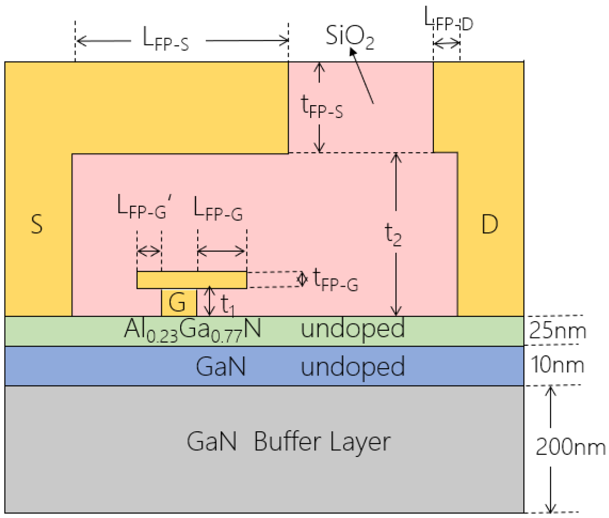
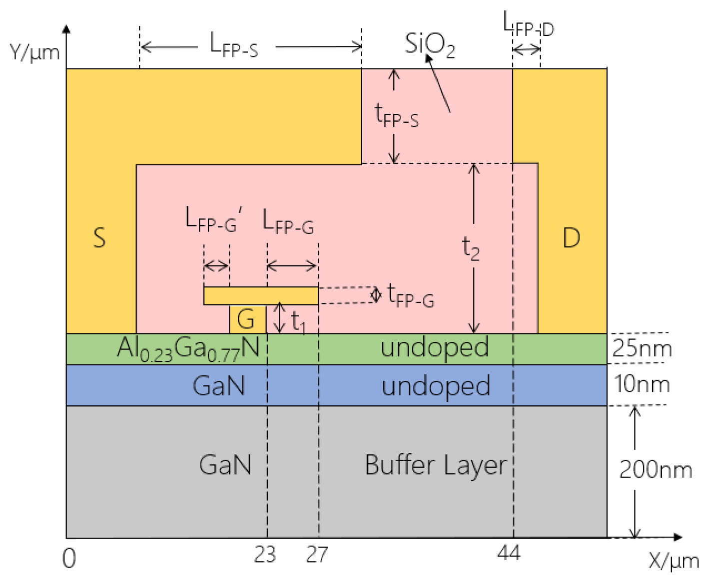
The two-dimensional numerical simulations were carried out by Silvaco TCAD. The simulated model was based on the experimental structure. Figure 1 shows a not-to-scale cross-section view of the device structure analyzed in this paper. The gate length LG was 3 μm, the source-to-gate distance LSG was 9 μm, and the gate-to-drain distance LGD was 22 μm. The field-plate length LFP-G’ was 2 μm. The insulator was assumed to be SiO2 in this simulation, which was usually used in our lab. The permittivity of SiO2 was set to 5, corresponding to the value of the experimental measurement. Likewise, Si3N4 [25] and Al2O3 [26] could also be selected as passivation, and the kind of insulator would not change the trend of VBD versus FPs [19]. The thickness of insulator layer t1 and t2; length of FPs LFP-G, LFP-S and LFP-D; and the thickness of FPs tFP-G and tFP-S are variable in the following Section. The leakage current [27], especially from the buffer layer, may result in electron injection from the channel into the buffer layer and a large drain current [28]. Setting traps in the GaN buffer is a usual way to decrease the leakage current at pinch-off state [19,29,30], but it may cause a no-convergence problem. Moreover, we aimed to present the relevance between electric field distributions and FPs clearly and exclude the punch-through from the buffer layer. Therefore, with the purpose of simplifying calculation, we set the GaN buffer layer to be 200 nm, reducing the influence of buffer leakage current flow from source to drain [31]. Besides, the thicknesses of the Al0.23Ga0.77N barrier and GaN channel are 25 nm and 10nm respectively.
Detailed simulation conditions are as follows. The 1×1013 cm−2 positive charges were placed along the Al0.23Ga0.77N/GaN heterojunction to create the two-dimension electron gas, and the channel mobility was set to 1500 cm2/V·s [32]. Also, the field-dependent mobility model and Shockley-Read-Hall (SRH) Recombination model were used. Thermal impact is common in the experiments [33,34], but we did not discuss it during the simulation. The breakdown voltage simulation in this paper was based on the Selberherr’s impact ionization model. The ionization coefficients were AN = AP = 2.98 × 10⁸ and BN = BP = 3.44 × 10⁷ [35]. Moreover, simulations about breakdown performance were all carried out with the gate biased at −6 V, keeping devices on the off-state. Finally, VBD was defined as the drain voltage when the peak electric field in the channel reached 3 MV/cm [10,14,22].
3. Influences of Structural Parameters of Different Field-Plates
3.1. Gate Field-Plate
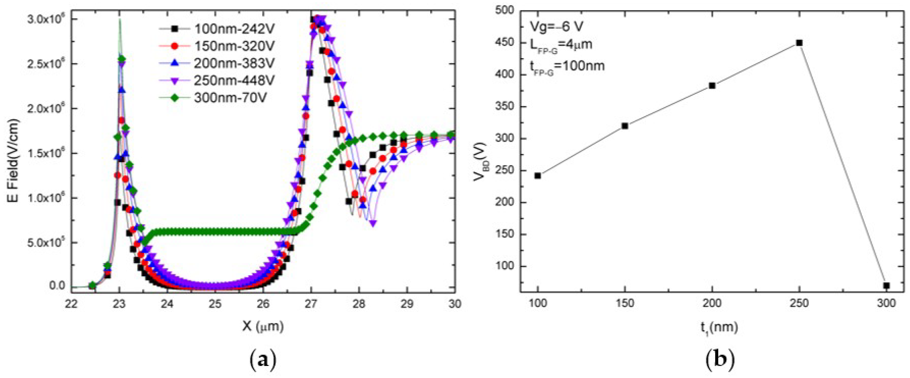
We first discuss the influence of gate field-plate on VBD. Figure 2 shows the device structure only with FP-G. Three parameters are studied, including the insulator layer thickness t1, the FP-G length LFP-G and the FP-G thickness tFP-G. Figure 3a shows the distributions of electric field along the heterojunction interface for t1 from 100 nm to 300 nm when LFP-G is 4μm and tFP-G is 100 nm. For the sake of presenting the electric field peaks intuitively, we only display the electric field distributions partly around the region from gate to drain. As shown in Figure 3a, for thin insulator layer t1 (t1 < 250 nm), the electric field at the FP-G edge is higher than the electric field at the gate edge. Due to the modulation of FP-G, the electric field at the FP-G edge reaches the breakdown standard first. Consequently, VBD increases with the increase of t1. However, when t1 further increases, the modulated effect of FP-G becomes weaker. Thus, the electric field peak shifts to the gate edge, which leads to the decrease of VBD. For the structure in Figure 2, the modulate effect induced by FP-G is optimal when t1 = 250 nm, as shown in Figure 3b.
Then, we change the LFP-G from 0 μm to 20 μm and keep t1 fixed at 250 nm. Without a field plate at the drain side, the electric field at the gate edge increases rapidly and reaches the critical breakdown field 3 MV/cm at around VD = 55 V. For short LFP-G (LFP-G<4 μm), the modulate effect of field-plate is too small to reduce the electric field peak at the gate edge, so VBD increases slowly with the increase of LFP-G. As shown in Figure 3c,d, with the optimized t1, LFP-G from 4 μm to 8 μm, all can reduce the electric field peak value along the channel effectively, and the electric field peak value of the gate edge reaches 3 MV/cm until VD = 448 V. When the LFP-G is more than 20 μm, VBD will decrease. It is attribute to the narrower distance between the field-plate edge and the drain, which leads to the electric field at the FP-G edge reaches the critical breakdown electric field at around VD = 435 V.
The following parameter is FP-G thickness tFP-G. It is set to 100 nm, 300 nm, 400 nm, 800 nm and 8 μm, respectively. In previous researches, there were few studies on the relationship between breakdown characteristics and the thickness of the field-plate. As shown in Figure 3e, VBD increases with the increase of tFP-G. This phenomenon shows that thicker FP-G can reduce the electric field at the FP-G edge. However, the improvement of VBD is not obvious even when the tFP-G reaches 8 μm. In view of the highest VBD achievement with less changes in technology progress, we choose tFP-G = 100 nm as a suitable value for following researches.
3.2. Source Field-Plate
The FP-S is usually used in the GaN-based HEMTs in combination with the gate field-plate, with the aim of achieving a great improvement of VBD. Figure 4 shows the structure with FP-S. Firstly, the relationship between FP-S and VBD is studied in the HEMT without the FP-G. The thickness of the gate was fixed at 100 nm. From Figure 5, the effect of FP-S on VBD is similar to that of FP-G. With regard to t2, the optimum value of t2 is less than that of t1. Because in this device, when the FP-G is fixed to −6 V, the FP-S is fixed to 0 V, resulting in a higher electric field at the FP-S edge than that at the FP-G edge. Hence, to achieve the same effect of modulating the electric field by FP, the FP-S should be closer to the AlGaN surface. The variation trend of VBD with the length and thickness of FP-S is the same as that of FP-G. As we know, the electric field is in direct proportion to the electric potential difference, and the latter can be performed by the density of the potential line distribution. Therefore, the higher electric field corresponds to the narrower potential lines. From the potential line distributions of Figure 5g,h, we find that potential lines in (g) of FP-G edge are less crowded than that in (h) of FP-S edge even at high drain voltage, which is in accordance with electric field distributions [11]. In a word, in order to enhance VBD, FP-G is more efficient than FP-S when the structure only has one FP.
3.3. Drain Field-Plate
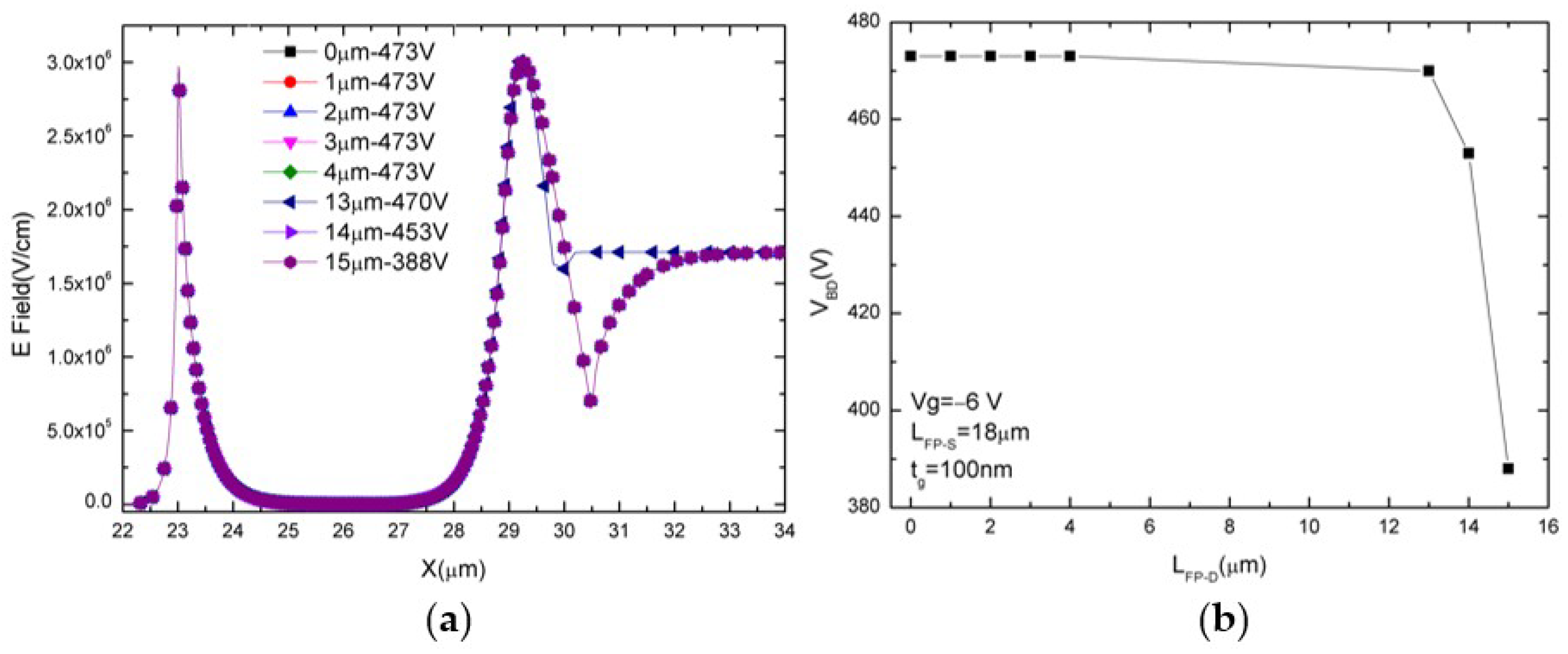
For FP-D, it is usually used to improve the reverse breakdown voltage. In fact, the electric field peak from the metal peak introduced by annealing could also be reduced by FP-D. However, the electric field peak does not appear on the drain edge in the Silvaco simulation, because of the flat and smooth edge of ohmic electros. Thus, single FP-D usually has little impact on electric field distribution along the channel. However, the electric field peak at the FP-S edge will increase if the distance between FP-S and FP-D is too close. Therefore, we only explored the relationship between FP-D length and VBD when the structure has both FP-S and FP-D, as shown in Figure 6. Figure 7 shows that when LFP-D>13 μm, VBD decreases due to the narrow distance between the two FPs. In consideration of passivation quality in the practical experiment, breakdown may occur between the two FPs. So, it may be more appropriate when LFP-D is set to 1 μm.
4. Devices Contained with FP-G, FP-S, and FP-D
For much higher VBD, there is no doubt that the FP-G should be combined with the FP-S [20]. Figure 8 shows the structure of the device contained with FP-G, FP-S and FP-D simultaneously. The VBD is affected by seven variables, t1, t2, LFP-G, LFP-S, LFP-D, tFP-G, and tFP-S. Since many parameters should be optimized, the procedure is significant. Because the electric field peak at the gate edge is mainly affected by FP-G, it can be suppressed by a moderate value of t1, LFP-G and tFP-G. Therefore, we can fix these three parameters to adjust the electric field peak at the gate edge, close to but not higher than 3 M/cm. At the same time, less changes in the previous structure and little influence of FP thickness in enhancing VBD, tFP-S and LFP-D can be confirmed too. Thus, we can confirm five parameter values firstly, as shown in Table 1 Then we can focus on the other two parameters, t2 and LFP-S.
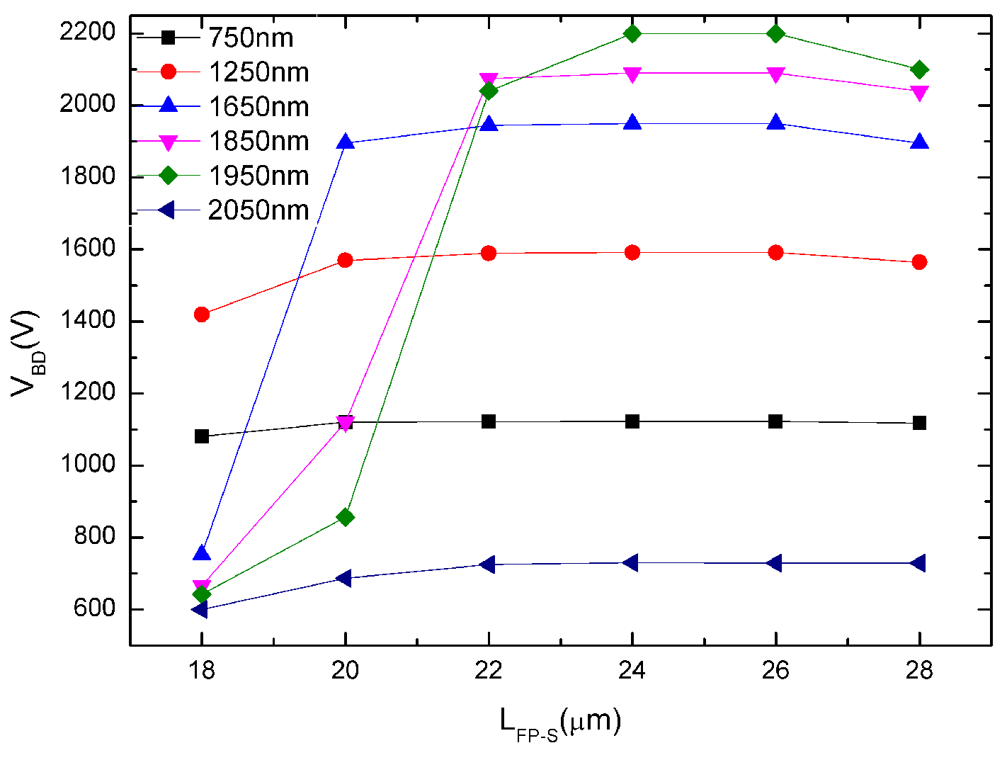
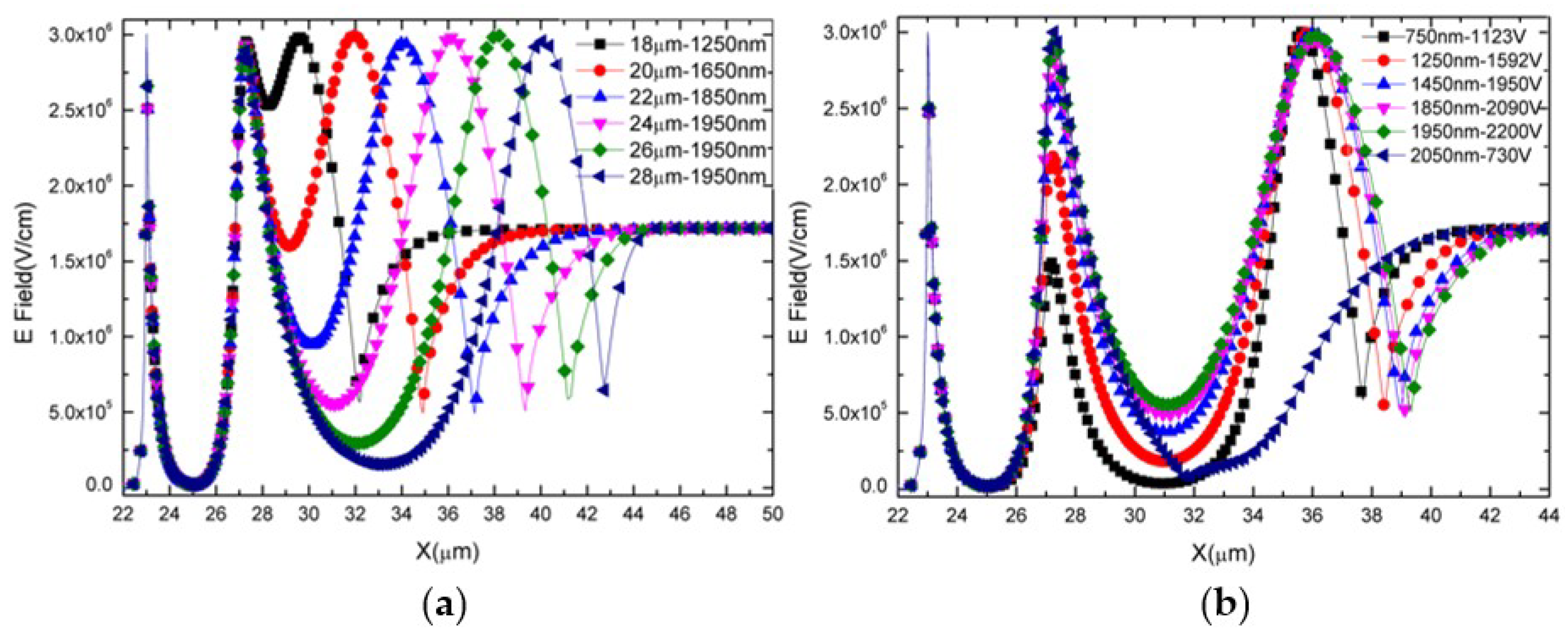
As shown in Figure 9, for different LFP-S which vary from 18 μm to 28 μm, the moderated value (up to the highest VBD) of t2 is different. We can find the reason in Figure 10a. Only when three peaks are uniform and close to 3 MV/cm, could we achieve the highest VBD. Meanwhile, comparing Figure 11a with Figure 11b, the potential lines distribution of the former are more crowded than that of the latter, resulting in a lower VBD [14].
However, no matter what the value of t2 is, there is the highest VBD of all lengths for a FP-S of 24 μm. When LFP-S is between 24 μm to 26 μm, combined with the optimal t2 = 1.7 μm, we can acquire the highest VBD of 2200 V. Then, when LFP-S is 28 μm, due to the narrow distance between FP-S and FP-D, the electric field peak of the FP-S edge will become higher, which makes VBD decrease. Figure 10b shows the electric field distributions for different t2 along the channel in HEMT when LFP-S is fixed to 24 μm. When t2 = 1950 nm, the two electric field peaks of FP-G edge and FP-S edge are approximate but not high enough to cause breakdown. So, when VBD is around 2200 V, the highest electric field peak appears at the gate edge. Hence, the crucial way to enhance breakdown voltage is to adjust relative FP parameters. By means of t2 and LFP-S, the two electric field peaks at each FPs edge could be uniformed to be closely equal but less than 3 M/cm; and if the highest electric field peak appears at the gate edge, we would acquire the highest VBD.
5. Conclusions
In this paper, the effect of geometrical variables of FP and insulator layer on field distribution and VBD were investigated systematically. An AlGaN/GaN HEMT with FP-G, FP-S and FP-D simultaneously was also studied. On account of the incorporation of three FPs, the structure becomes more complex, and more parameters are needed for it to be optimized. Therefore, systematic simulation of these parameters could provide a correct direction for the design of a practical device. By Silvaco TCAD, we optimize the length of FPs, thickness of FPs, and the insulator layer, and acquire the highest VBD = 2200 V. The mechanism of VBD enhancement by inducing FPs is the effective modulation of potential lines distribution in the channel. By studying the potential lines and electric field distribution along the AlGaN/GaN heterojunction interface, we can draw some conclusions. In terms of kinds of FP, FP-G can modulate potential lines distribution more uniformly and suppress the electric field peak at FP edge more effectively, compared with FP-S and FP-D. In terms of multiple field-plate combinations, the crucial way to enhance breakdown voltage is to adjust the relative FP parameters. Consequently, the electric field peaks at gate edge, FP-G edge and FP-S edge are uniform to be closely equal but lower than 3 M/cm. Particularly, LFP-S and t2 play the most important roles in modulating electric field peaks at FP-G and FP-S edge. Furthermore, the field-plate thickness should be taken into account for the inducing field-plate, in which the breakdown voltage increases with the increase of the field-plate thickness.
Author Contributions
Conceptualization, B.L. and Q.Z.; methodology, B.L. and J.Q.; validation, Q.Z.; formal analysis, B.L. and Q.Z.; writing—original draft preparation, B.L. and Q.Z.; writing—review and editing, H.W.; supervision, H.W.
Funding
This work was supported by Science and Technologies plan Projects of Guangdong Province (Nos. 2017B010112003, 2017A050506013), and by Applied Technologies Research and Development Projects of Guangdong Province (Nos. 2015B010127013, 2016B010123004), and by Science and Technologies plan Projects of Guangzhou City (Nos. 201504291502518, 201604046021, 201704030139, 201905010001), and by Science and Technology Development Special Fund Projects of Zhongshan City (Nos. 2017F2FC0002, 2017A1009).
Conflicts of Interest
The authors declare no conflict of interest. The funders had no role in the design of the study.
References
- Mishra, U.K.; Shen, L.; Kazior, T.E.; Wu, Y.F. GaN-Based RF Power Devices and Amplifiers. Proc. IEEE 2008, 96, 287–305. [Google Scholar] [CrossRef]
- Liu, Y.; Chai, C.; Chunlei, S.; Fan, Q.; Liu, Y. Optimization design on breakdown voltage of AlGaN/GaN high-electron mobility transistor. J. Semicond. 2016, 37, 40–44. [Google Scholar] [CrossRef]
- Zeng, F.; An, J.X.; Zhou, G.; Li, W.; Wang, H.; Duan, T.; Jiang, L.; Yu, H. A Comprehensive Review of Recent Progress on GaN High Electron Mobility Transistors: Devices, Fabrication and Reliability. Electronics 2018, 7, 377. [Google Scholar] [CrossRef]
- Kuzuhara, M.; Asubar, J.T.; Tokuda, H. AlGaN/GaN high-electron-mobility transistor technology for high-voltage and low-on-resistance operation. Jpn. J. Appl. Phys. 2016, 55, 070101. [Google Scholar] [CrossRef] [Green Version]
- Karmalkar, S.; Mishra, U.K. Enhancement of breakdown voltage in AlGaN/GaN high electron mobility transistors using a field plate. IEEE Trans. Electron Devices 2001, 48, 1515–1521. [Google Scholar] [CrossRef]
- Zhang, N.Q.; Keller, S.; Parish, G.; Heikman, S.; Denbaars, S.; Mishra, U.K. High. breakdown GaN HEMT with overlapping gate structure. IEEE Electron Device Lett. 2000, 21, 421–423. [Google Scholar] [CrossRef]
- Bahat-Treidel, E.; Hilt, O.; Brunner, F.; Sidorov, V.; Würfl, J.; Tränkle, G. AlGaN/GaN/AlGaN DH-HEMTs Breakdown Voltage Enhancement Using Multiple Grating Field Plates (MGFPs). IEEE Trans. Electron Devices 2010, 57, 1208–1216. [Google Scholar] [CrossRef]
- Bahat-Treidel, E.; Sidorov, V.; Würfl, J.; Tränkle, G. Simulation of AlGaN/GaN HEMTs’ Breakdown Voltage Enhancement Using Grating Field Plates. Simul. Semicond. Process. Devices 2007, 277–280. [Google Scholar] [CrossRef] [Green Version]
- Dora, Y.; Chakraborty, A.; McCarthy, L.; Keller, S.; Denbaars, S.P.; Mishra, U.K. High Breakdown Voltage Achieved on AlGaN/GaN HEMTs With Integrated Slant Field Plates. IEEE Electron Device Lett. 2006, 27, 713–715. [Google Scholar] [CrossRef]
- Kong, X.; Wei, K.; Liu, G.-G.; Liu, X.-Y. Improvement of breakdown characteristics of an AlGaN/GaN HEMT with a U-type gate foot for millimeter-wave power application. Chin. Phys. B 2012, 21, 128501. [Google Scholar] [CrossRef]
- Mao, W.; She, W.-B.; Yang, C.; Zhang, C.; Zhang, J.-C.; Ma, X.-H.; Zhang, J.-F.; Liu, H.-X.; Yang, L.-A.; Zhang, K.; et al. A two-dimensional fully analytical model with polarization effect for off-state channel potential and electric field distributions of GaN-based field-plated high electron mobility transistor. Chin. Phys. B 2014, 23, 87305. [Google Scholar] [CrossRef]
- Kaddeche, M.; Telia, A.; Soltani, A. Modeling of AlGaN/GaN HEMTs using field-plate technology. In Proceedings of the 2009 3rd International Conference on Signals, Circuits and Systems (SCS), Medenine, Tunisia, 6–8 November 2009; pp. 1–4. [Google Scholar]
- Wu, W.-H.; Lin, Y.-C.; Chin, P.-C.; Hsu, C.-C.; Lee, J.-H.; Liu, S.-C.; Maa, J.S.; Iwai, H.; Chang, E.Y.; Hsu, H.T. Reliability improvement in GaN HEMT power device using a field plate approach. Solid-State Electron. 2017, 133, 64–69. [Google Scholar] [CrossRef]
- Mao, W.; Fan, S.-J.; Du, M.; Zhang, J.-F.; Zhang, J.-C.; Zheng, X.-F.; Wang, C.; Ma, X.-H.; Zhang, J.-C.; Hao, Y. Analysis of the modulation mechanisms of the electric field and breakdown performance in AlGaN/GaN HEMT with a T-shaped field-plate. Chin. Phys. B 2016, 25, 127305. [Google Scholar] [CrossRef]
- Amit, M.; Rawal, D.S.; Sharma, S.; Kapoor, S.; Liashram, R.; Chaubey, R.K.; Vinayak, S.; Sharma, R.K. Design and Fabrication of Multi-finger Field Plate for Enhancement of AlGaN/GaN HEMT Breakdown Voltage. Defence Sci. J. 2018, 68, 290. [Google Scholar] [CrossRef]
- Saito, W.; Nitta, T.; Kakiuchi, Y.; Saito, Y.; Tsuda, K.; Omura, I.; Yamaguchi, M. Suppression of Dynamic On-Resistance Increase and Gate Charge Measurements in High-Voltage GaN-HEMTs With Optimized Field-Plate Structure. IEEE Trans. Electron Devices 2007, 54, 1825–1830. [Google Scholar] [CrossRef]
- Benny Sathish, M.; Fletcher, A.S.A. Design and modeling of HEMT using field plate technique. In Proceedings of the 2017 International Conference on Innovations in Electrical, Electronics, Instrumentation and Media Technology (ICEEIMT), Coimbatore, India, 3–4 February 2017; pp. 157–159. [Google Scholar] [CrossRef]
- Uemoto, Y.; Shibata, D.; Yanagihara, M.; Ishida, H.; Matsuo, H.; Nagai, S.; Batta, N.; Li, M.; Ueda, T.; Tanaka, T.; et al. 8300 V Blocking Voltage AlGaN/GaN Power HFET with Thick Poly-AlN Passivation. In Proceedings of the 2007 IEEE International Electron. Devices Meeting, Washington, DC, USA, 10–12 December 2007; pp. 861–864. [Google Scholar]
- Kabemura, T.; Ueda, S.; Kawada, Y.; Horio, K. Enhancement of Breakdown Voltage in AlGaN/GaN HEMTs: Field Plate Plus High-k Passivation Layer and High Acceptor Density in Buffer Layer. IEEE Trans. Electron Devices 2018, 65, 3848–3854. [Google Scholar] [CrossRef]
- Aamir Ahsan, S.; Ghosh, S.; Sharma, K.; Dasgupta, A.; Khandelwal, S.; Chauhan, Y.S. Capacitance Modeling in Dual Field-Plate Power GaN HEMT for Accurate Switching Behavior. IEEE Trans. Electron Devices 2016, 63, 565–572. [Google Scholar] [CrossRef]
- Saito, W.; Kuraguchi, M.; Takada, Y.; Tsuda, K.; Omura, I.; Ogura, T. Design Optimization of High Breakdown Voltage AlGaN–GaN Power HEMT on an Insulating Substrate for RONA-VB Tradeoff Characteristics. IEEE Trans. Electron Devices 2005, 52, 106–111. [Google Scholar] [CrossRef]
- Mao, W.; She, W.-B.; Yang, C.; Zhang, J.-F.; Zheng, X.-F.; Wang, C.; Hao, Y. Reverse blocking characteristics and mechanisms in Schottky-drain AlGaN/GaN HEMT with a drain field plate and floating field plates. Chin. Phys. B 2016, 25, 017303. [Google Scholar] [CrossRef]
- Lian, Y.-W.; Lin, Y.-S.; Lu, H.-C.; Huang, Y.-C.; Hsu, S.S.H. AlGaN/GaN HEMTs on Silicon With Hybrid Schottky–Ohmic Drain for High Breakdown Voltage and Low Leakage Current. IEEE Electron Device Lett. 2012, 33, 973–975. [Google Scholar] [CrossRef]
- Silvaco TCAD. Version 2016 Software for DC, AC and Transient Analysis for Compound Semiconductor Devices; Silvaco Inc.: Santa Clara, CA, USA, 2016. [Google Scholar]
- Hu, J.; Stoffels, S.; Lenci, S.; Bakeroot, B.; De Jaeger, B.; Van Hove, M.; Ronchi, N.; Venegas, R.; Liang, H.; Zhao, M.; et al. Performance Optimization of Au-Free Lateral AlGaN/GaN Schottky Barrier Diode with Gated Edge Termination on 200-mm Silicon Substrate. IEEE Trans. Electron Devices 2016, 63, 997–1004. [Google Scholar] [CrossRef]
- Zhe, C.; Yun, Z.; Lian, Z.; Zhao, Y.B.; Wang, J.X.; Li, J.M. Normally-off recessed MOS-gate AlGaN/GaN HEMTs with over +4 V saturation drain current density and a 400 V breakdown voltage. In Proceedings of the China International Forum on Solid State Lighting: International Forum on Wide Bandgap Semiconductors, Beijing, China, 15–17 November 2016. [Google Scholar]
- Hu, J.; Lenci, S.; Stoffels, S.; Jaeger, B.D.; Groeseneken, G.; Decoutere, S. Leakage-current reduction and improved on-state performance of Au-free AlGaN/GaN-on-Si Schottky diode by embedding the edge terminations in the anode region. Phys. Status Solidi C 2014, 11, 862–865. [Google Scholar] [CrossRef]
- Hanawa, H.; Onodera, H.; Nakajima, A.; Horio, K. Numerical Analysis of Breakdown Voltage Enhancement in AlGaN/GaN HEMTs With a High-k Passivation Layer. IEEE Trans. Electron Devices 2014, 61, 769–775. [Google Scholar] [CrossRef]
- Chvála, A.; Nagy, L.; Marek, J.; Priesol, J.; Donoval, D.; Blaho, M.; Gregušová, D.; Kuzmík, J.; Šatka, A. Characterization of Monolithic InAlN/GaN NAND Logic Cell Supported by Circuit and Device Simulations. IEEE Trans. Electron Devices 2018, 65, 2666–2669. [Google Scholar] [CrossRef]
- Horio, K.; Yonemoto, K.; Takayanagi, H.; Nakano, H. Physics-based simulation of buffer-trapping effects on slow current transients and current collapse in GaN field effect transistors. J. Appl. Phys. 2005, 98, 124502. [Google Scholar] [CrossRef]
- Hanawa, H.; Horio, K. Increase in breakdown voltage of AlGaN/GaN HEMTs with a high-kdielectric layer. Phys. Status Solidi A 2014, 211, 784–787. [Google Scholar] [CrossRef]
- Shealy, J.R.; Prunty, T.R.; Chumbes, E.M.; Ridley, B.K. Growth and passivation of AlGaN/GaN heterostructures. J. Cryst. Growth 2003, 250, 7–13. [Google Scholar] [CrossRef]
- Xu, Z.; Zhou, Y.; Li, J. 200 °C normally off AlGaN/GaN MISFET with 321 mA/mm drain current density and 1055 V breakdown voltage. Electron. Lett. 2019, 55, 282–283. [Google Scholar] [CrossRef]
- Aminbeidokhti, A.; Dimitrijev, S.; Han, J.; Chen, X.; Xu, X. The Power Law of Phonon-Limited Electron Mobility in the 2-D Electron Gas of AlGaN/GaN Heterostructure. IEEE Trans. Electron Devices 2016, 63, 2214–2218. [Google Scholar] [CrossRef]
- Kunihiro, K.; Kasahara, K.; Takahashi, Y.; Ohno, Y. Experimental evaluation of impact ionization coefficients in GaN. IEEE Electron Device Lett. 1999, 20, 608–610. [Google Scholar] [CrossRef]
Figure 1.
Schematic of HEMT with FP-G, FP-S and FP-D.

Figure 2.
Device structure with FP-G analyzed in this study.

Figure 3.
The electric field distributions along the channel for different values of (a) t1, (c) LFP-G, and (e) tFP-G. The VBD for different values of (b) t1, (d) LFP-G, and (f) tFP-G.
Figure 3.
The electric field distributions along the channel for different values of (a) t1, (c) LFP-G, and (e) tFP-G. The VBD for different values of (b) t1, (d) LFP-G, and (f) tFP-G.


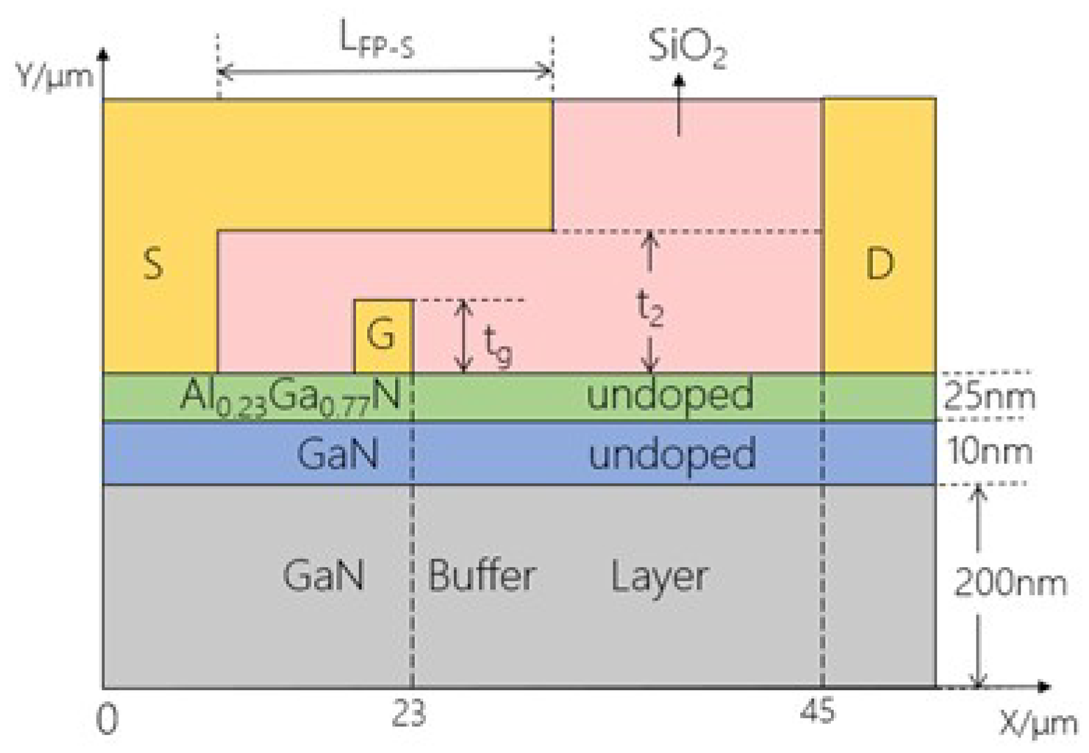
Figure 4.
Device structure with FP-S analyzed in this study.

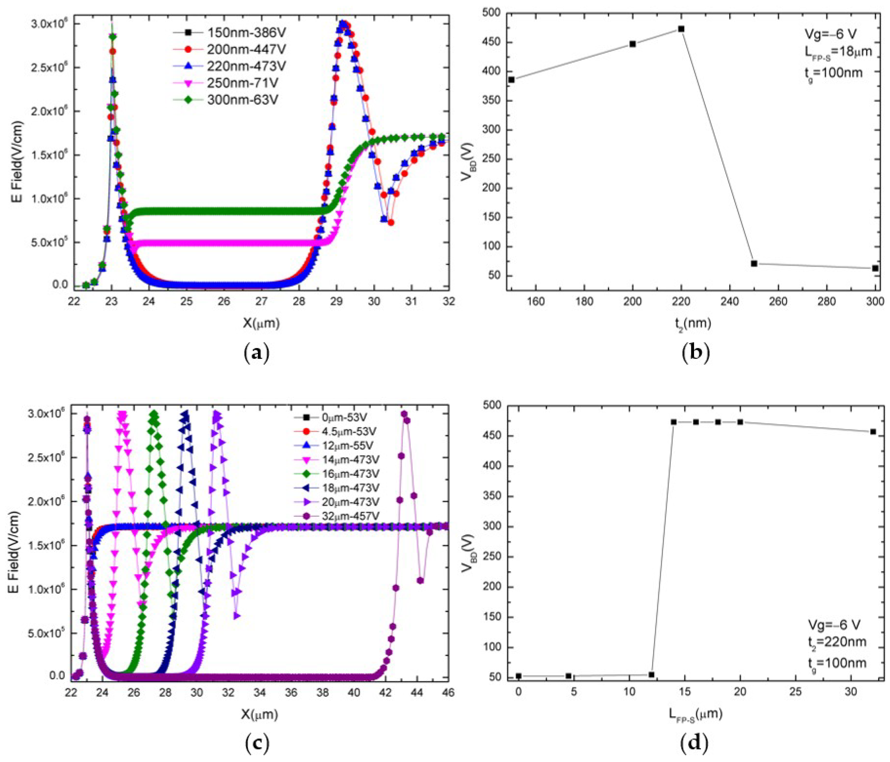
Figure 5.
The electric field distributions along the channel for different values of (a) t2, (c) LFP-S, and (e) tFP-S. Off-state breakdown voltage VBD for different values of (b) t2, (d) LFP-S, and (f) tFP-S. The Potential line distributions along the channel when (g) t1 = 250 nm, LFP-G = 4 μm, tFP-G = 1.4 μm, VBD = 521 V, and (h) t2 = 120 nm, LFP-S = 18 μm, tFP-S = 1.4 μm, VBD = 473 V.


Figure 6.
Device structure with FP-S and FP-D analyzed in this study.

Figure 7.
The electric field distributions along the channel for different values of (a) LFP-D. Off-state breakdown voltage VBD for different values of (b) LFP-D.
Figure 7.
The electric field distributions along the channel for different values of (a) LFP-D. Off-state breakdown voltage VBD for different values of (b) LFP-D.

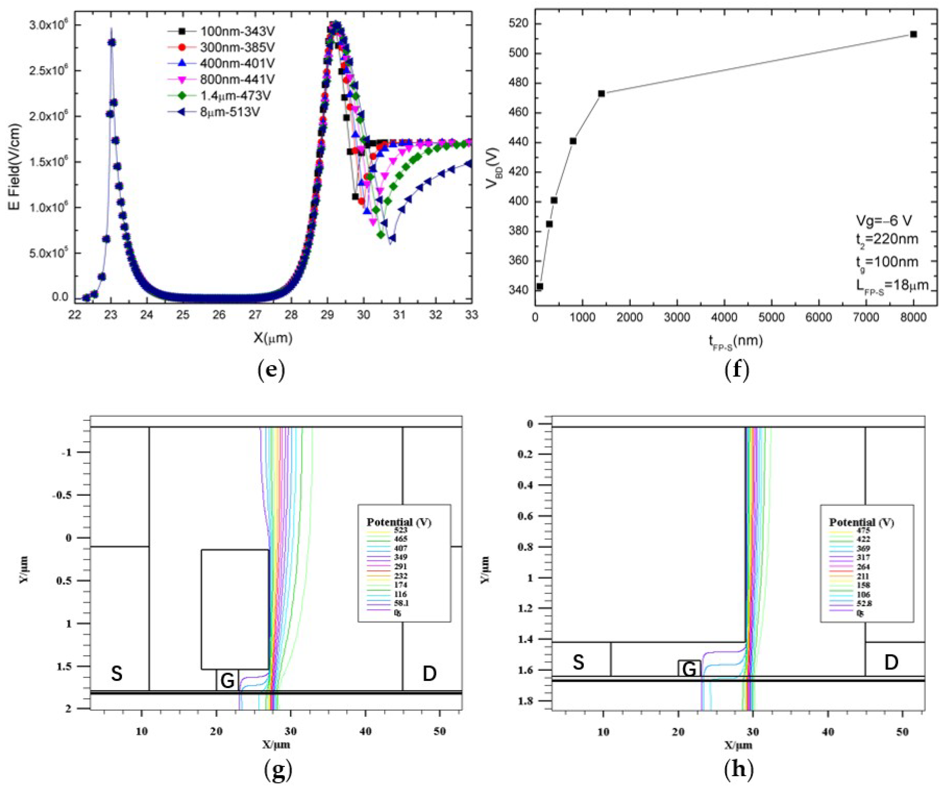
Figure 8.
Device structure contained with FP-G, FP-S, and FP-D.

Figure 9.
VBD as a function of t2 and LFP-S.

Figure 10.
(a) The electric field distributions along the channel in HEMT with different LFP-S under highest VBD; (b) the electric field distributions along the channel in HEMT when LFP-S = 24.
Figure 10.
(a) The electric field distributions along the channel in HEMT with different LFP-S under highest VBD; (b) the electric field distributions along the channel in HEMT when LFP-S = 24.

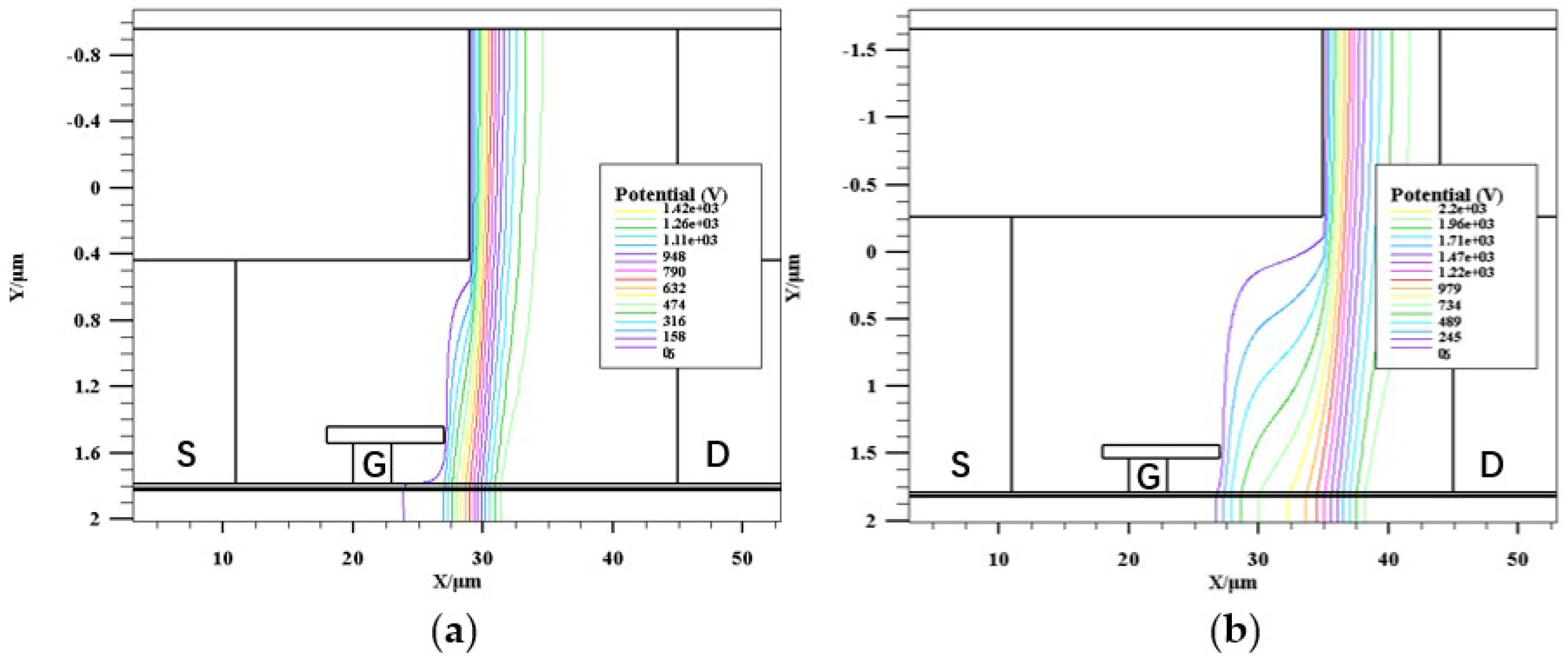
Figure 11.
The Potential distributions in HEMT. (a) LFP-S = 18 μm with t2 = 1250 nm at VBD = 1420 V; (b) LFP-S = 24 μm with t2 = 1950 nm at VBD = 2200 V.
Figure 11.
The Potential distributions in HEMT. (a) LFP-S = 18 μm with t2 = 1250 nm at VBD = 1420 V; (b) LFP-S = 24 μm with t2 = 1950 nm at VBD = 2200 V.


Table 1.
Optimized parameter values.
| Parameter | Optimized Value |
|---|---|
| t1 | 250 nm |
| LFP-G | 4 μm |
| tFP-G | 100 nm |
| tFP-S | 1.4 μm |
| LFP-D | 1 μm |
© 2019 by the authors. Licensee MDPI, Basel, Switzerland. This article is an open access article distributed under the terms and conditions of the Creative Commons Attribution (CC BY) license (http://creativecommons.org/licenses/by/4.0/).
Share and Cite
MDPI and ACS Style
Liao, B.; Zhou, Q.; Qin, J.; Wang, H. Simulation of AlGaN/GaN HEMTs’ Breakdown Voltage Enhancement Using Gate Field-Plate, Source Field-Plate and Drain Field Plate. Electronics 2019, 8, 406. https://doi.org/10.3390/electronics8040406
AMA Style
Liao B, Zhou Q, Qin J, Wang H. Simulation of AlGaN/GaN HEMTs’ Breakdown Voltage Enhancement Using Gate Field-Plate, Source Field-Plate and Drain Field Plate. Electronics. 2019; 8(4):406. https://doi.org/10.3390/electronics8040406
Chicago/Turabian StyleLiao, Biyan, Quanbin Zhou, Jian Qin, and Hong Wang. 2019. "Simulation of AlGaN/GaN HEMTs’ Breakdown Voltage Enhancement Using Gate Field-Plate, Source Field-Plate and Drain Field Plate" Electronics 8, no. 4: 406. https://doi.org/10.3390/electronics8040406
Note that from the first issue of 2016, this journal uses article numbers instead of page numbers. See further details here.