A New Method to Extract Gate Bias-Dependent Parasitic Resistances in GaAs pHEMTs


Key Laboratory of Ocean Observation-Imaging Testbed of Zhejiang Province, Institute of Marine Electronic and Intelligent System, Ocean College, Zhejiang University, Zhoushan 316021, China
*
Authors to whom correspondence should be addressed.
Electronics 2019, 8(3), 266; https://doi.org/10.3390/electronics8030266
Submission received: 24 January 2019
/
Revised: 20 February 2019
/
Accepted: 25 February 2019
/
Published: 28 February 2019
(This article belongs to the Section Microwave and Wireless Communications)
Abstract
:Accurate large signal GaAs pHEMT models are essential for devices’ performance analysis and microwave circuit design. This, in turn, mandates precise small signal models. However, the accuracy of small signal models strongly depends on reliable parasitic parameter extraction of GaAs pHEMT, which also greatly influences the extraction of intrinsic elements. Specifically, the parasitic source and drain resistances, and , are gate bias-dependent, due to the two-dimensional charge variations. In this paper, we propose a new method to extract and directly from S-parameter measurements of the device under test (DUT), which save excessive measurements and complicated parameter extraction. We have validated the proposed method in both simulation and on-wafer measurement, which achieves better accuracy than the existing state-of-the-art in a frequency range of 0.5–40 GHz. Furthermore, we develop a GaAs pHEMT power amplifier (PA) to further validate the developed model. The measurement results of the PA at 9–15 GHz agree with the simulation results using the proposed model.
1. Introduction
Compared with the widely-used 4G mobile communication, 5G has obvious advantages in large-scale antenna arrays, resource utilization, transmission rate, and spectrum utilization. The capacity of 5G is 1000-times that of 4G, and the peak rate can reach 10 Gbps. In order to overcome the disadvantages of poor penetration ability and small coverage due to high frequency in 5G communication, a radio-frequency (RF) power amplifier must deliver high efficiency and linearity. 5G power amplifiers (PAs) used in microcell and macrocells need to provide high , which can be realized by GaAs or GaN [1]. In order to achieve high output power and efficiency, a 5G microcell/macrocell often utilizes GaAs pHEMTs due to their superior frequency response, breakdown performance, high charge density, and high electron mobility. In turn, an accurate and reliable GaAs pHEMT model is needed.
A number of available models for III-V devices have been published, such as physics-based models [2,3], ANNs-based models [4,5], and empirical-based models [6,7,8]. ANNs-based models are not physical and often result in a slow convergence in the simulation. Physical-based models are complicated and could lead to long simulation times. In contrast, high-fidelity empirical-based compact models (i.e., equivalent circuit models) are desirable. First, an empirical-based compact model is simple and can facilitate simulations. Second, an empirical-based compact model offers a relatively smaller set of parameters, simplifying extraction and still abiding by device physics. Third, empirical-based compact models are scalable with regard to bias, temperature, and dimension, which is design friendly.
A large signal nonlinear model mandates a precise small signal model. However, the precision of small signal model strongly relies on parasitic parameter extraction of a GaAs pHEMT. In this paper, we focus on the extraction method for parasitic source and drain resistances, and . In [6,7,8,9,10,11], and were determined by S-parameters in the “cold” pinch-off condition, wherein the drain-to-source bias was set to zero, and the gate electrode was in a pinch-off condition. The use of “ColdFET” measurements assumes that and are bias-independent. However, this assumption is not accurate because the space-charge layer extends into the gate-drain region and is also changed due to the two-dimensional charge control when the device gate bias varies [12]. Therefore, and are gate bias-dependent. In III-V devices, the parasitic resistances and are closely related to and . For the electrons in the gate-source or gate-drain channel, a reduction in electron mobility () induces an increase in and [12]. The increase in and leads to a drop of and [13,14,15]. In PAs, the output signal strength and linearity are determined by the input signal and device . Hence, it is preferred that remains constant [16,17]. However, the drop of and induces gain reduction and seriously affects large signal linearity [17,18]. Therefore, the gate bias-dependent parasitic resistances and play a key role in the nonlinearity of GaAs pHEMTs.
Aiming at analyzing the transistor performance, several methods have been developed in order to obtain and from experimental devices [12,19,20,21]. Pradeep [12] proposed a DC method to yield , , and versus simultaneously in an HEMT by using the - curves at a low drain-source voltage, , of this device (short HEMT) and a much longer channel HEMT (long HEMT) and transfer length measurements (TLM) on ungated devices. However, this method mandates sophisticated DC measurements. The method in [19] uses the Y-function curve to obtain the series resistance through the curve of total resistance as a function of the inverse of the Y-function. The Y-function is calculated by , where is the transconductance obtained by the derivative of with respect to . However, this calculation process is complex and tends to introduce errors. A majorization of the iterative method was proposed in [20], where the complete process was iterated with an updated value until internal consistency was achieved between the newly-determined and the updated seed value . Obviously, this procedure needs a long calculating time. In Torres’s method [21], two identical capacitances = were used to describe the depletion-layer in strong inversion at = 0 V. This method is based on a common assumption, that the gate-to-source and gate-to-drain depletion-layer capacitances are equal for a symmetrical device structure in strong inversion. However, this assumption is not appropriate for pHEMTs due to the pHEMT devices’ asymmetry [7,8].
In order to save excessive measurements and complicated parameter optimization, we propose a new method to determine and . The method utilizes desired device operation in strong inversion and attains on-wafer S-parameter measurements to derive and . The proposed method is verified in both simulation and on-wafer measurement, which achieves better accuracy than the existing state-of-the-art in a frequency range of 0.5–40 GHz. Furthermore, we develop a GaAs pHEMT PA to further validate the proposed method. The measurement results of the PA at 9–15 GHz agree well with the simulation results of the proposed method, which indicates the accuracy of the model and the effectiveness of the proposed extract method.
The remainder of this article is organized as follows. Section 2 is dedicated to the detailed extraction step of parasitic parameters and . Section 3 describes the test bench we built to verify the proposed method, and we discuss the results of the proposed model by comparing it with measurement data. The concluding remarks are drawn in the last section.
2. Modeling and
As mentioned before, the prior state-of-the-art used “ColdFET” measurements [6,7,8,9,10,11], assumed and as bias-independent, DC measurements [12,19], needed complicated DC measurements, iterative optimization [20], needed a complex calculation process and S-parameter measurements [21], used invalid assumptions, etc. To simplify the test steps and save parameter extraction time, we proposed a new parameter extraction method to obtain and .
The source and drain resistances, and , are different due to the pHEMT devices’ asymmetry. and both can be treated as two parts: the first part describes the parasitic effect of contact resistance and is assumed to be constant. The second part describes the resistance between source or drain contact at one side and the beginning of the space charge region below gate at the other side, which charges with gate bias, due to the two-dimensional charge control. In terms of the description above, we write and as [12]:
where and represent the gate bias independent and dependent components of the source resistance, respectively. and represent the gate bias independent and dependent components of the drain resistance, respectively.
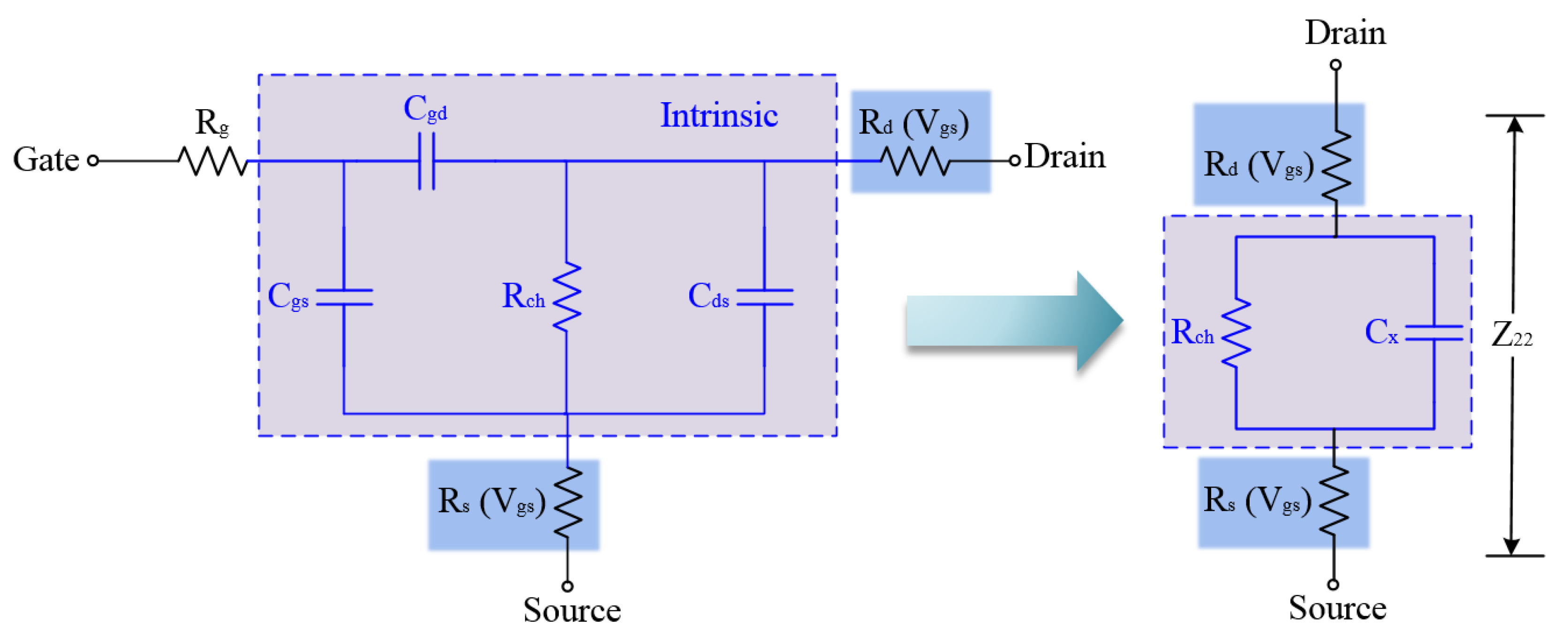
In this work, a new extraction method is proposed for GaAs pHEMTs. Similar to the extraction of parasitic resistance for MOSFETs in [21], transconductance () is negligible when a pHEMT is biased at = 0 V. Given this condition, a small signal equivalent circuit of the device is simplified as Figure 1. is the gate resistance, and , , and are the intrinsic capacitances between terminals. Z-parameters associated with the circuit of Figure 1 are given by:
Then, the real parts of the Z-parameters are expressed as:
where,
As shown in Equations (7)–(9), our primary task is to derive , A, and 1 + /. The value of 1 + / is deduced from the ratio of the imaginary part of and [22]. That is:
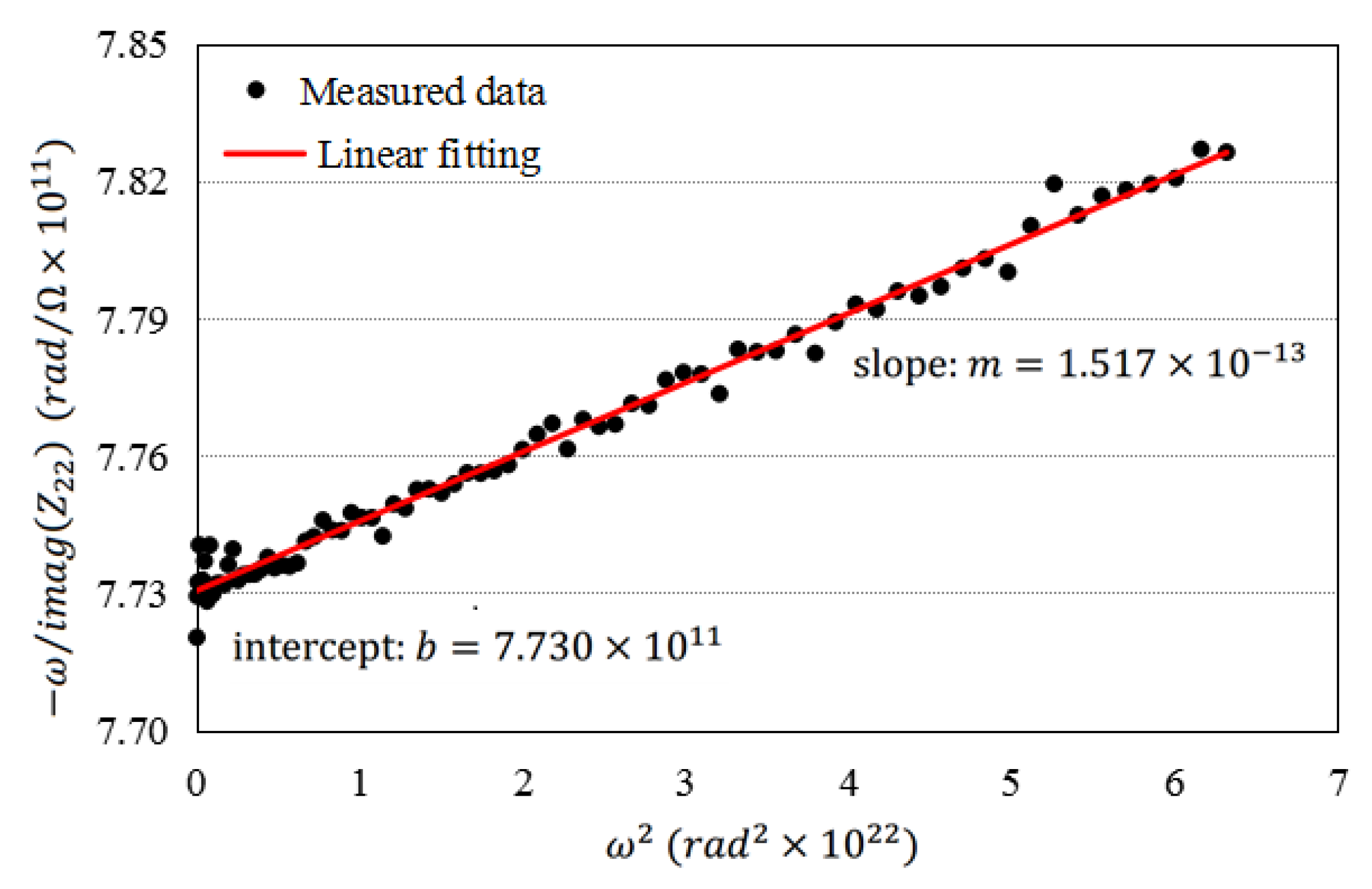
Prior works [21,22] calculated A based on the value of and , i.e., is determined from the slope m of the linear regression of against the curve, and is calculated from , where b is the extrapolation to = 0 of the linear regression. Figure 2 shows the figure to determine and for a pHEMT.
Subsequently, can be derived from:
The value of derived from A and 1 + / may introduce calculation errors. In order to resolve this issue, we directly extracted under the device pinched-off condition ( = 0, < ) [7,8] according to the assumption that parasitic resistance is bias independent. Different from the prior derivation, we can directly calculate A from the real part of and . Substituting Equation (12) into Equations (7) and (8), and were rewritten as:
Subsequently, we calculate A by solving Equations (15) and (16) and yield:
Once , A, and 1 + / are determined, and can be obtained by the following equations:
Consequently, we achieve a simple calculation and reduce derivation error. The parameter extraction uncertainty calculation is discussed in Appendix A.
3. Measurements
To validate the modeling and parameter extraction methodology proposed in this paper, a group of multi-finger microwave GaAs E-mode pHEMTs in a common source configuration with gate lengths = 0.15 m have been fabricated in a 0.15-m E-mode pHEMT GaAs process. For these devices, the per-finger channel-widths () were 25 m, 50 m, 75 m, and 100 m, and the number of fingers () were 2, 4, and 6, respectively.
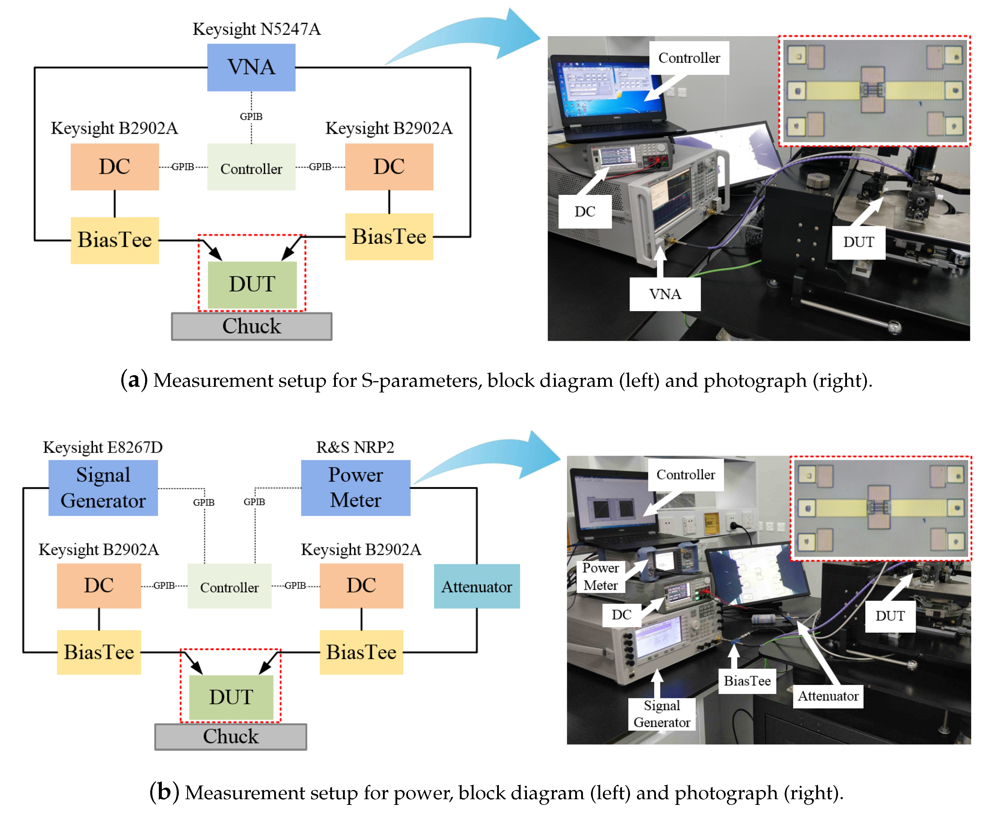
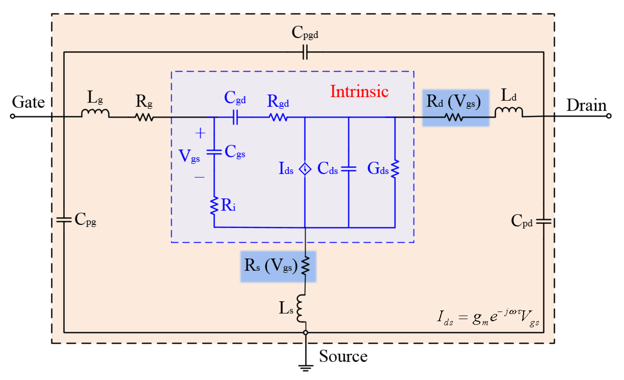
Figure 3 illustrates the setup of a measurement system for on-wafer RF measurements. A controller (Labview test program) sends commands to instruments (vector network analyzer (VNA), power signal generators (PSG), DC I-V supply, etc.). A probe station performs the measurements for a specific DUT and gathers measured data for post-processing. The DC characteristics of DUT are measured by the Keysight B2902A. The small signal behavior (i.e., S-parameter) of DUT is measured in a frequency range of 0.5–40 GHz by the Keysight N5247A VNA. Large signal performance of the DUT is measured by the Keysight E8267D PSG. The measurement system also used two 150 m pitch ground-signal-ground (GSG) probes for RF experiments and two Bias Tees for I-V curve measurement. To ensure the accuracy of measurements, a system-level calibration was performed before conducting any measurements on the DUT. Typically, system-level calibration for on-wafer measurements is done by the short-open-load-through (SOLT) algorithm to remove undesirable effects of cables and probes, as well as for establishing the reference impedance to 50 . In addition, a two-step de-embedding procedure using the measurements of on-wafer “open” and “short” dummy structures was carried out to subtract the test structures parasitic effect (TSPE) of probe pads and the interconnection line (i.e., representing the connection between the probe pads and the actual pHEMT) from measurements. Please bear in mind that the effect of the extrinsic pHEMT’s parasitics (e.g., the gate electrode resistance and capacitances, etc.) was not removed by the de-embedding procedure, as well as the dummy structures described in [23]. These measurements were performed up to 40 GHz under different bias conditions, varying from the subthreshold region to the saturation region. The small signal model in Figure 4 shows extrinsic elements (i.e., , ,, , , , , , and ) and intrinsic elements (i.e., , ,, , , , , and ).
A 4 × 50 m E-mode pHEMT was used in the extraction procedure. Before extracting and from RF measurements, TSPE had to be removed from experimental data [23]. The S-parameters of the pinched-off device ( = 0 V, = 0 V) were first taken and converted to equivalent admittance parameters to determine the parasitic capacitances [7,8]. Subsequently, the gate resistances and parasitic inductances were extracted by a “ColdFET” pinched-off method [7] after de-embedding the parasitic capacitors.
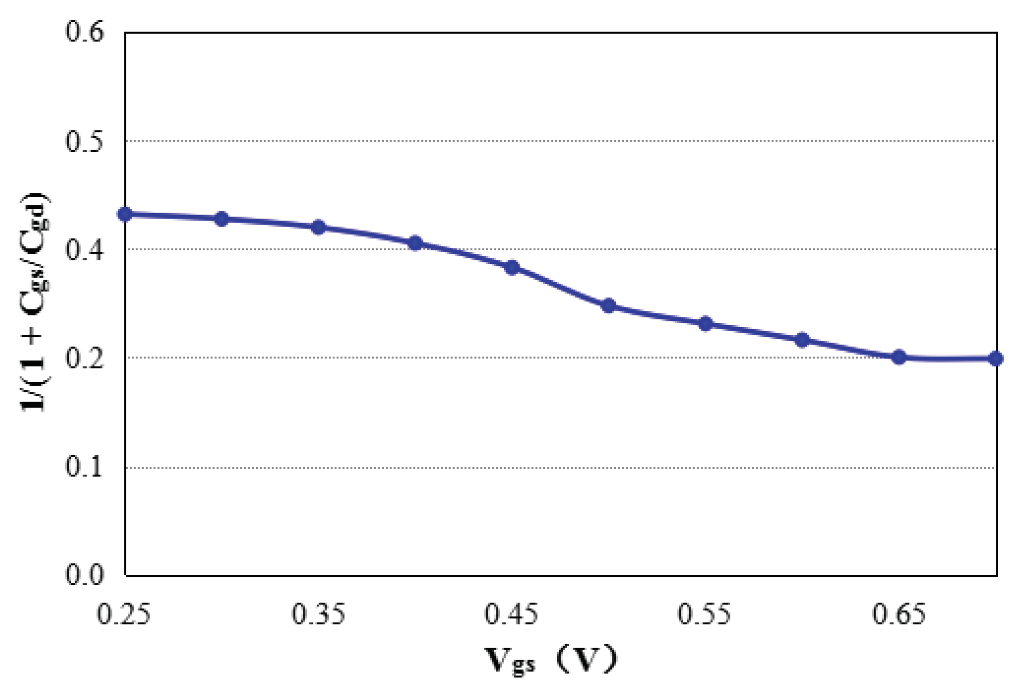
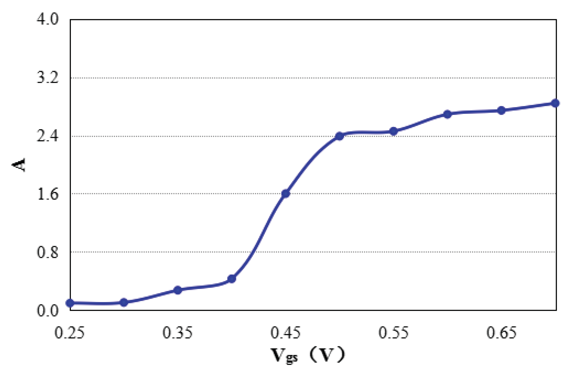
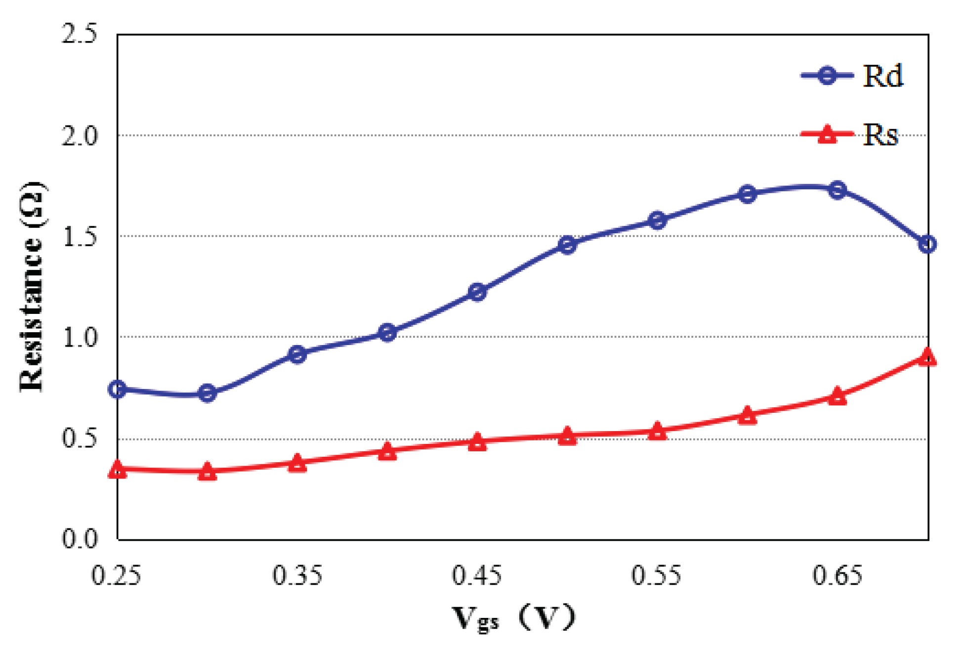
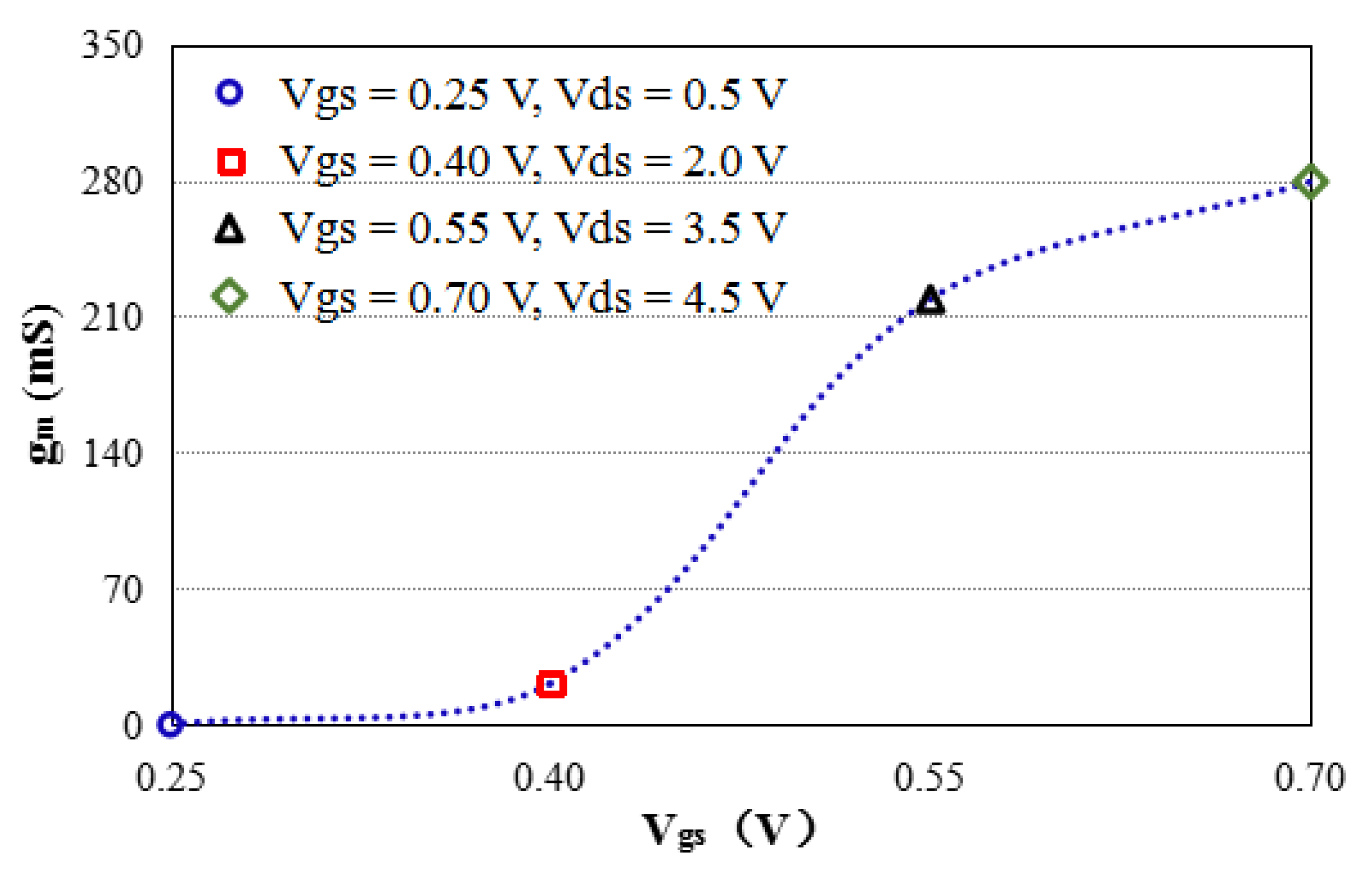
After we obtained the values of parasitic capacitances, parasitic inductances, and gate resistances, the proposed method was employed to extract and . Figure 5 shows the extracted value of 1/(1 + /). It is seen that the value of 1/(1 + /) is inversely proportional to . The bias-dependence of 1/(1 + /) shown in Figure 5 is associated with and . Because increases with dramatically, while changes slightly with , therefore / increases as a whole, meaning that 1/(1 + /) drops. Figure 5 also indicates that the assumption in [21] is not appropriate for pHEMTs [7,8]. Figure 6 shows that the value of A increases with . Because the term decreases with dramatically while increases with slightly, the term decreases and A increases accordingly with . Figure 7 shows the extracted and for different by the proposed method. Figure 7 shows that and increase with the rise of gate voltage, in which changes about 239% and changes about 270% with from 0.25 V–0.7 V. Since and are defined as the sum of contact resistance and bulk resistance up to the edge of the gate depletion region, the extracted bias-dependent and are consistent with the previously-described physical principle.
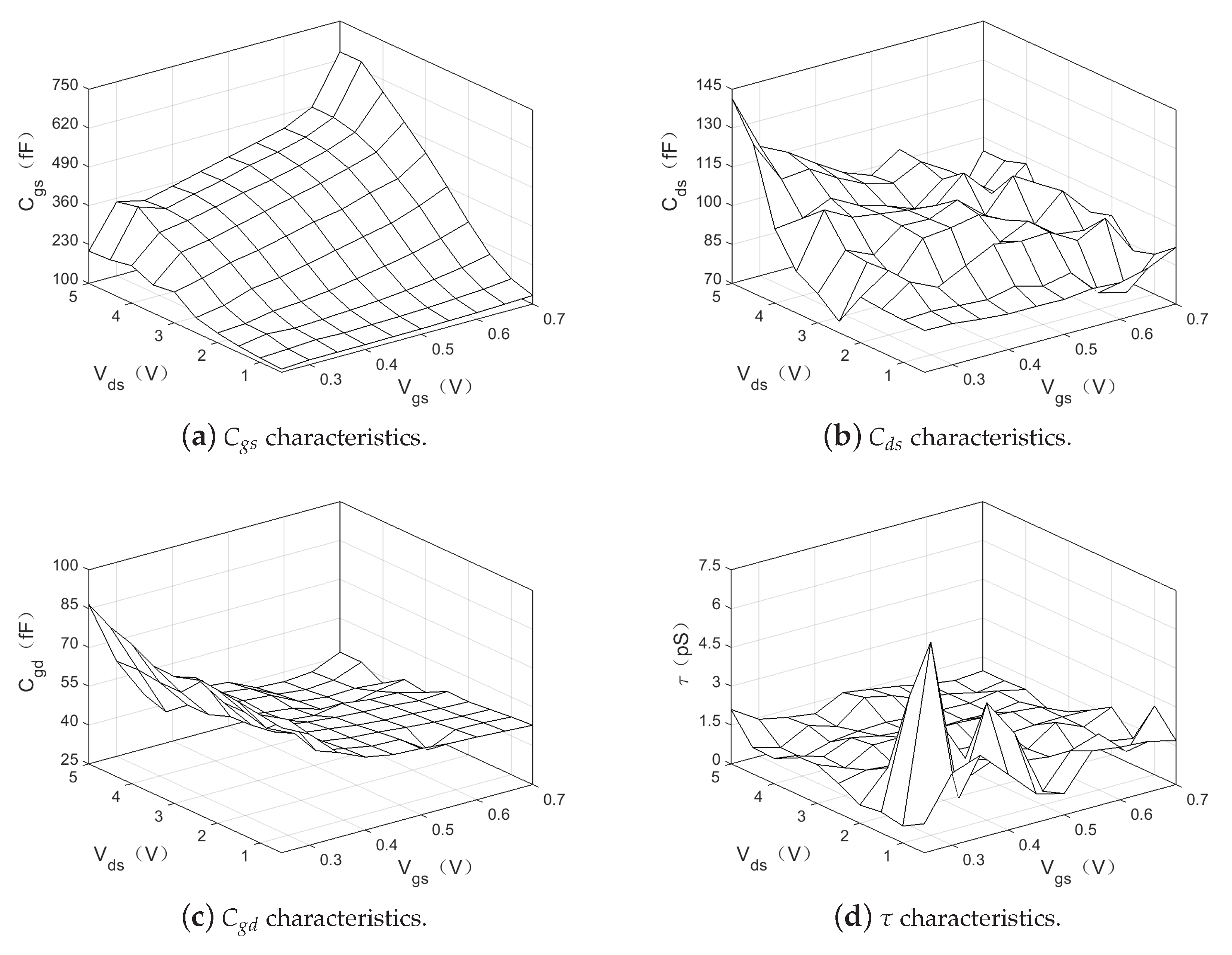
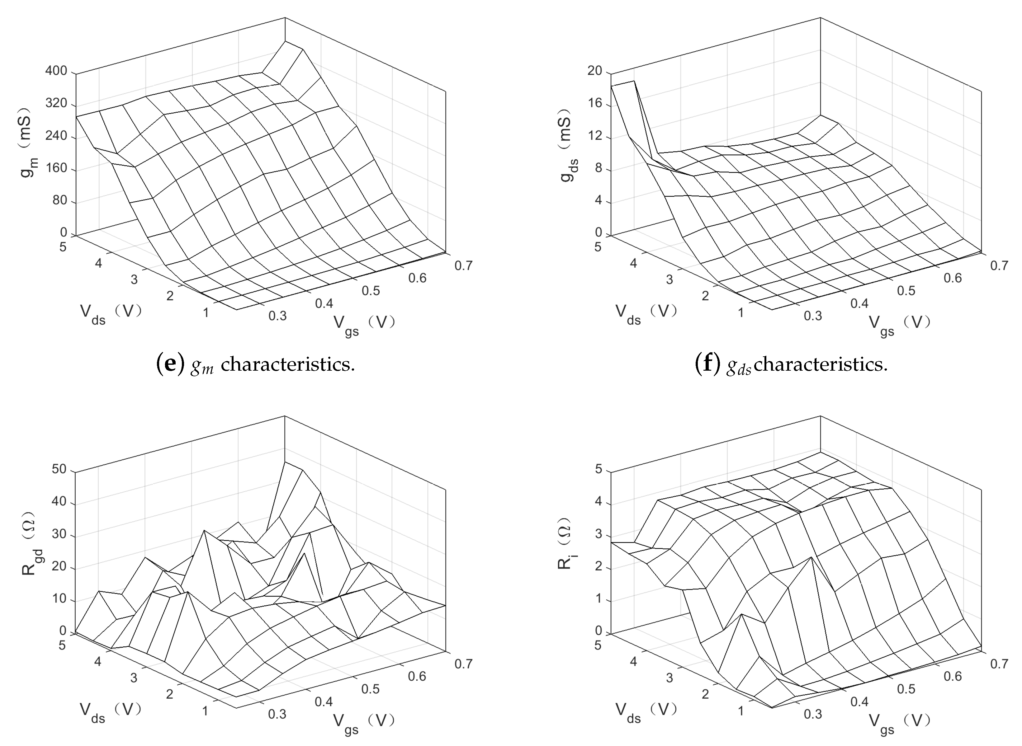
Once and have been extracted by the proposed method, the intrinsic elements’ values of the pHEMT can be directly extracted by the intrinsic Y-parameters [24]. Figure 8 displays the value of each intrinsic parameter at various biases ( = 0.25–0.7 V with an interval of 0.05 V and = 0.5–5 V with a step of 0.5 V). is low when the pHEMT is in the pinched-off region. rapidly increases after the pHEMT is turned on. is substantially constant near the saturation region. decreases as increases and varies slightly with . increases rapidly as increases. varies greatly in the linear region and is substantially constant in the saturation region. and are associated with . In addition, Figure 8a,c shows that is far less than for the pHEMTs and further verifies the assumption in [21] that it is not appropriate for pHEMTs [7,8].
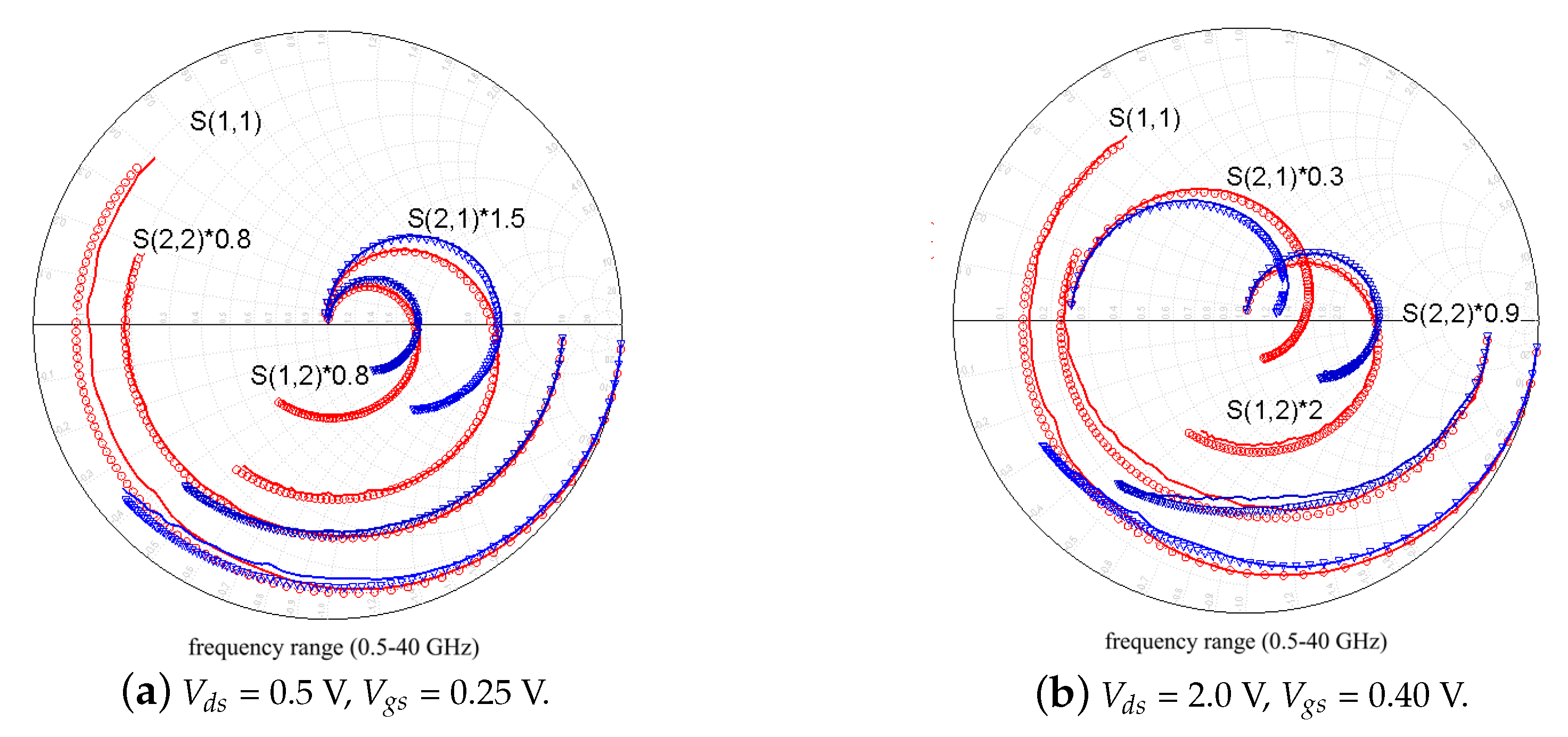
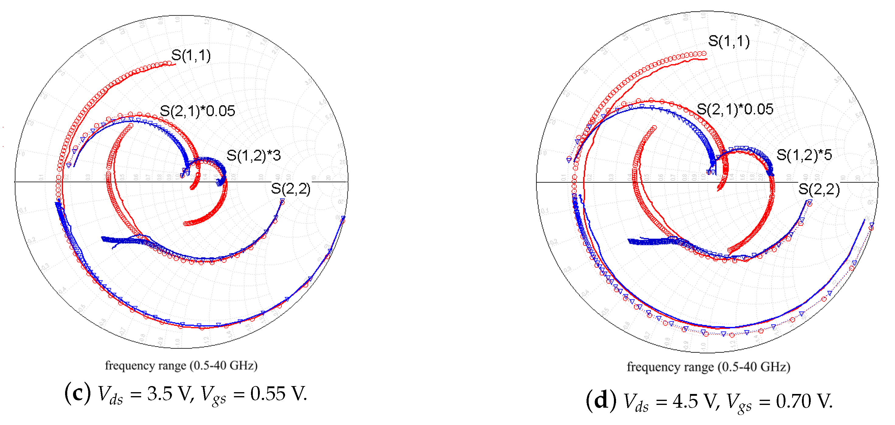
Figure 9 shows the comparison between measured and simulated S-parameters before and after applying the “open-short” de-embedding procedure. S-parameters are taken at different drain and gate voltages, where the DUT operates from the pinch-off region ( = 0.5 V, = 0.25 V) to the saturation region ( = 4.5 V, = 0.70 V). As can be clearly observed, significant changes in the behavior of the S-parameters were detected by de-embedding the contributions associated with the “open” and “short” dummy structures. The experimental results verify the validity of the proposed extraction method to determine small signal extrinsic elements. The measurements agree with the simulated S-parameters across the entire frequency and bias range.
As can be observed in Figure 9, the kink effect (KE) appears in only after de-embedding the extrinsic contributions for a certain bias point (i.e., Figure 9c,d). This is because the extrinsic contributions tend to mask the KE or even lead to its vanishing, and this finding is in line with the fact that the KE is inherently rooted in the intrinsic FET [9,25,26]. It was confirmed by previous studies that have already demonstrated that the appearance or disappearance of the KE in is mostly due to the relatively high [9,25,26]. Figure 10 shows the values of for pHEMT at four different bias conditions. As shown in Figure 9 and Figure 10, the KE in vanishes when is small, while the KE in appears when is large.
In order to evaluate the quantitative precision of the simulated S-parameter, the percentage error expression between simulated and measured S-parameters is defined as follows:
where and denote the frequency start point and stop point, respectively, presents the number of frequency points, and is 80 in this experiment. The total percentage error between models simulated and measured is formulated as follows:
The bias-dependent S-parameter simulation for the same device was performed at 100 bias points covering from 0.25–0.7 V and from 0.5–5 V with a frequency range from 0.5–40 GHz. This simulation was then compared with measured data.
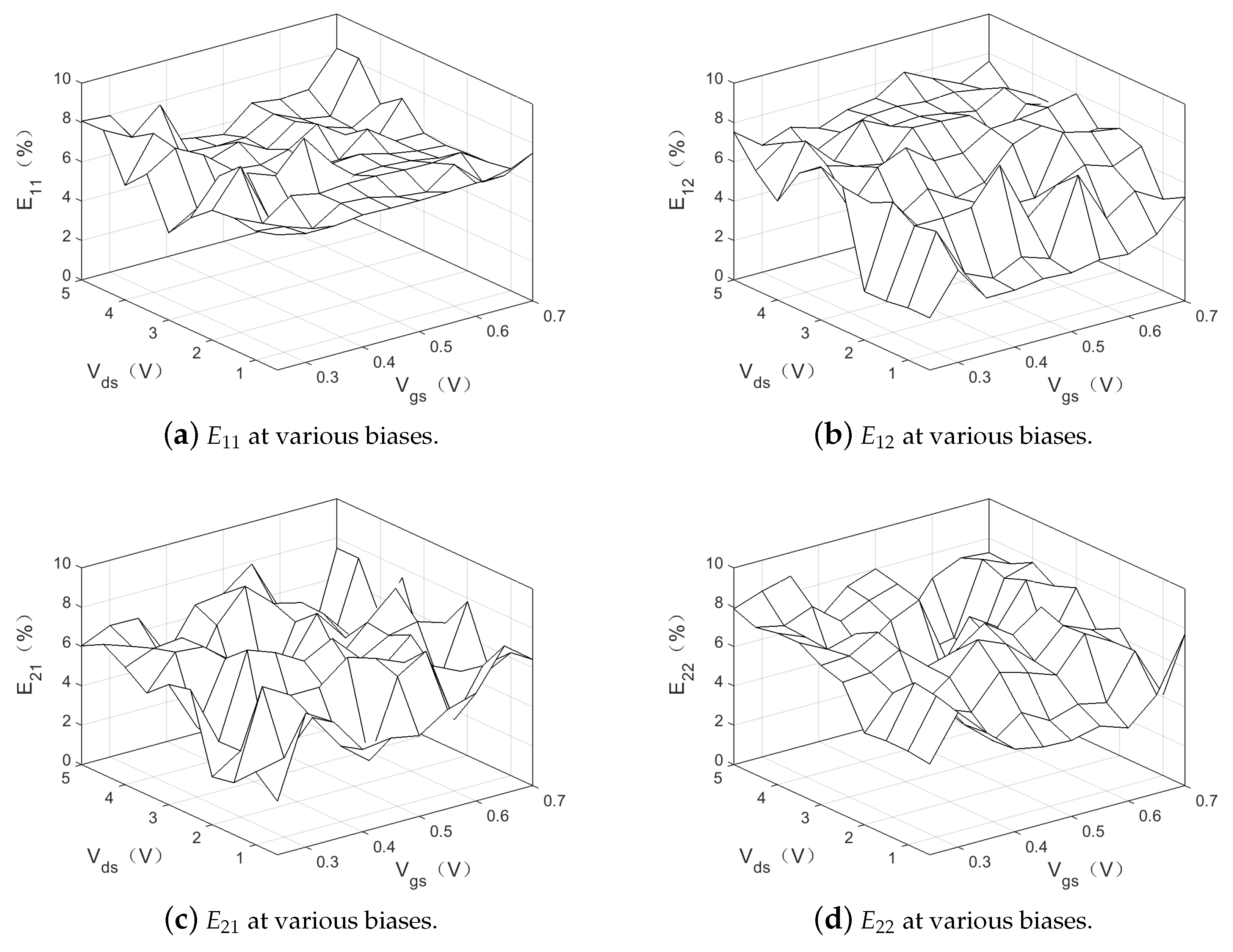
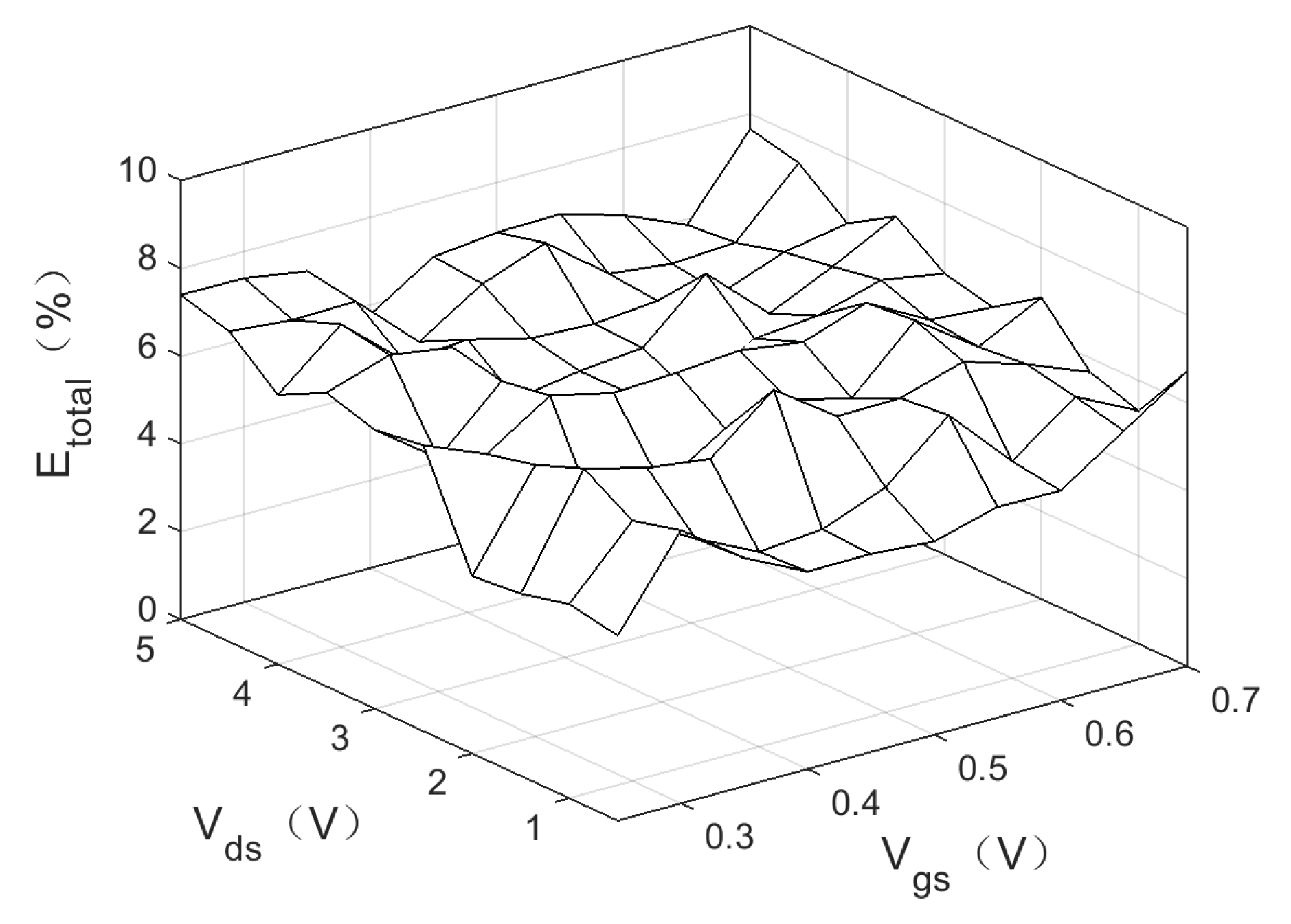
In Figure 11, the bias-dependent plots of are given. Figure 11a shows the percentage error of , where the minimum value is 4.43%, the average value is 6.53%, and the maximum value is 8.64%. It is clearly seen from the figure that the error in the entire saturation region is 4%–6%. Figure 11b illustrates the percentage error of . The error range when < 0.55 V was 2.46%–6.5%, which is acceptable. However, when > = 0.55 V, the error increased to at most 8.22%, because became smaller at high . Figure 11c illustrates the simulation error of , where the average error is 5.58% and the minimum error is 2.20%. It is shown that the error is pretty low except some discrete bias points, such as = 4.5V, = 0.5 V. Figure 11d illustrates the simulation error of , where the average error is 6.14% and the minimum value is 3.05%. It is shown that the measurement matches the simulation very well except some discrete bias points. In Figure 12, the bias-dependent plots of the total percentage error are given. The minimum value was 4.04%, the average error 6.07%, and the maximum error 7.65%. It is shown that the total percentage error is pretty low except some discrete bias points, such as = 1.0 V, = 0.7 V. Figure 11 and Figure 12 both illustrate that the measured S-parameters match the simulation results very well, which verifies the effectiveness of the proposed extract method.
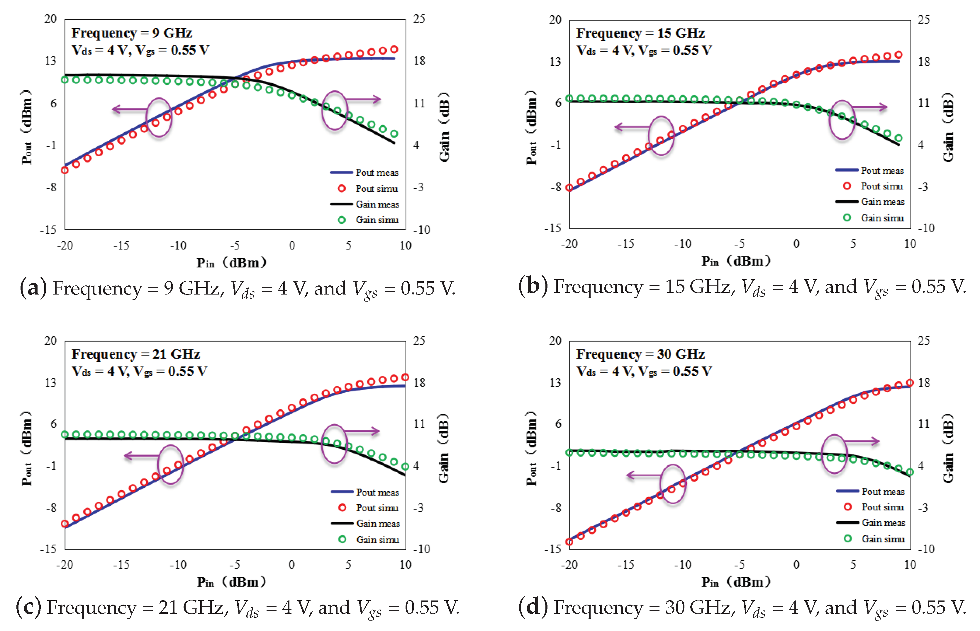
In order to further examine the precision of the small signal equivalent circuit model based on the proposed extraction method, a large signal model based on Verilog-A was built to estimate the large signal RF behavior of GaAs E-mode pHEMTs. Figure 13 compares the measured and simulated results of the output power for 4 × 50 m GaAs E-mode pHEMTs at = 4 V, = 0.55 V and frequency = 9, 15, 21, and 30 GHz, respectively. and gain-compression were accurately reproduced by the nonlinear model, which indicates an accurate nonlinear model and further verifies the effectiveness of the proposed extract method.
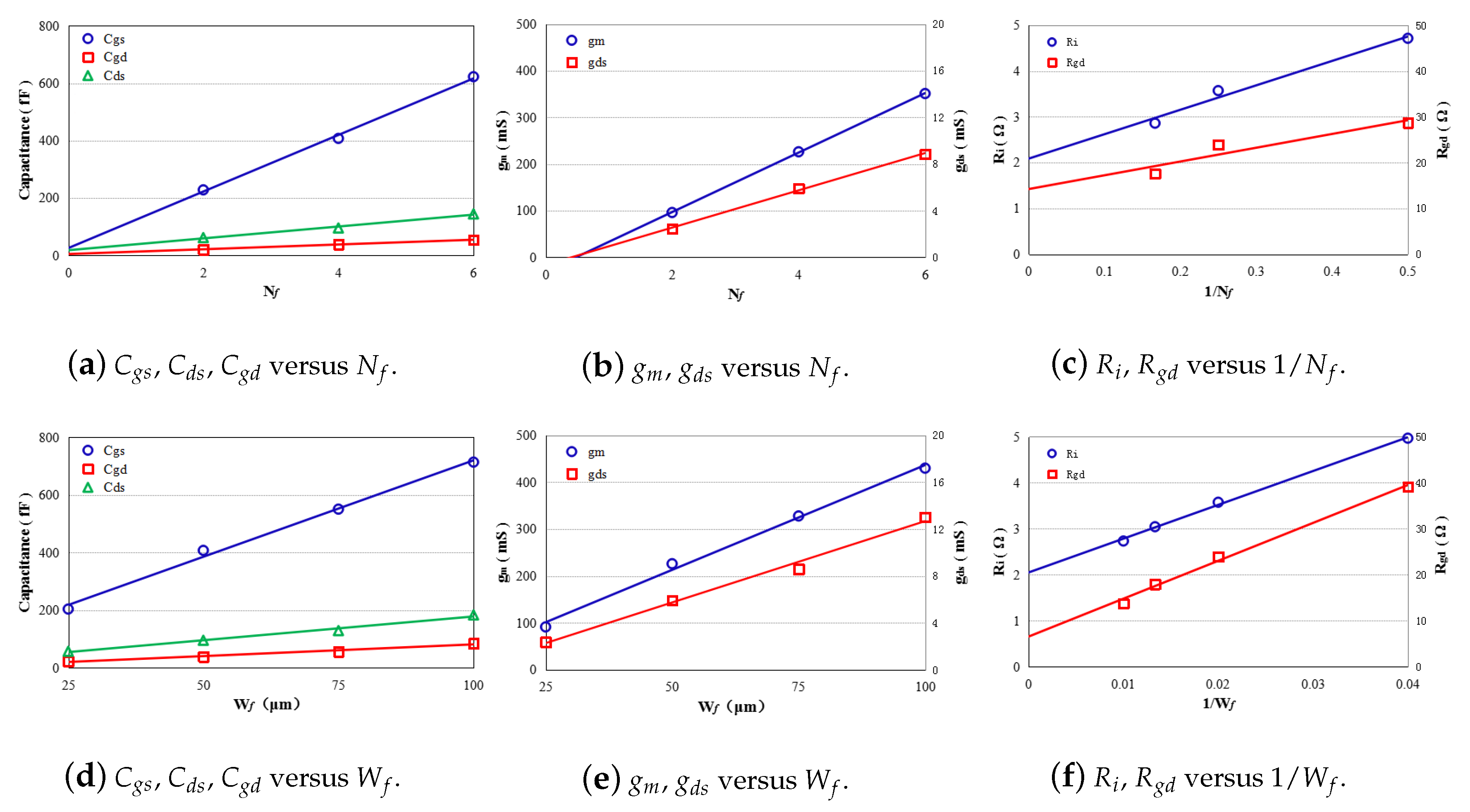
In order to make the model flexible and facilitate circuit design. We have investigated the scaling of the intrinsic elements with respect to and . In Figure 14, we plot , , , , , , and versus and at = 4 V and = 0.55 V, respectively. Figure 14a,b,d,e shows that , , , , and increase as and increase at the same bias condition. Figure 14c,f illustrates that and decrease as and increase at the same bias condition. Figure 14 directly demonstrates the linear scaling rule adopted for pHEMT. The total gate width () is straightforwardly proportional to these two parameters:
By doing so, we can build the scaling model for circuit design.
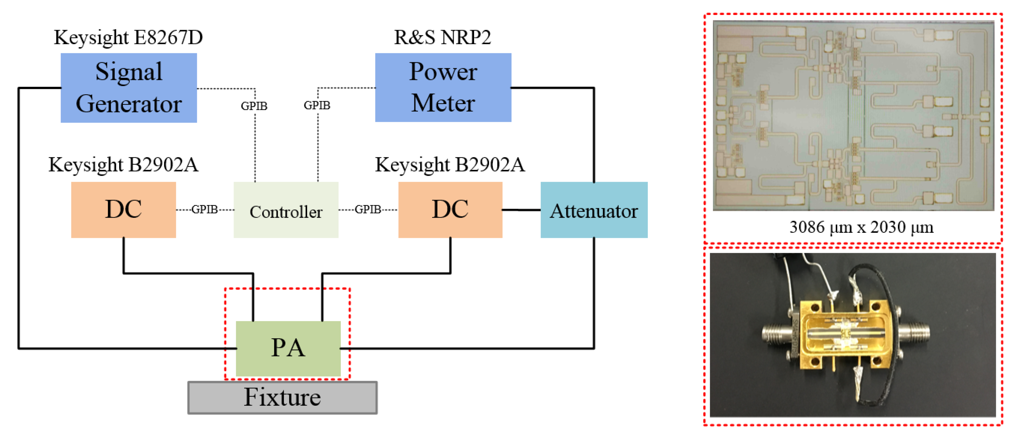
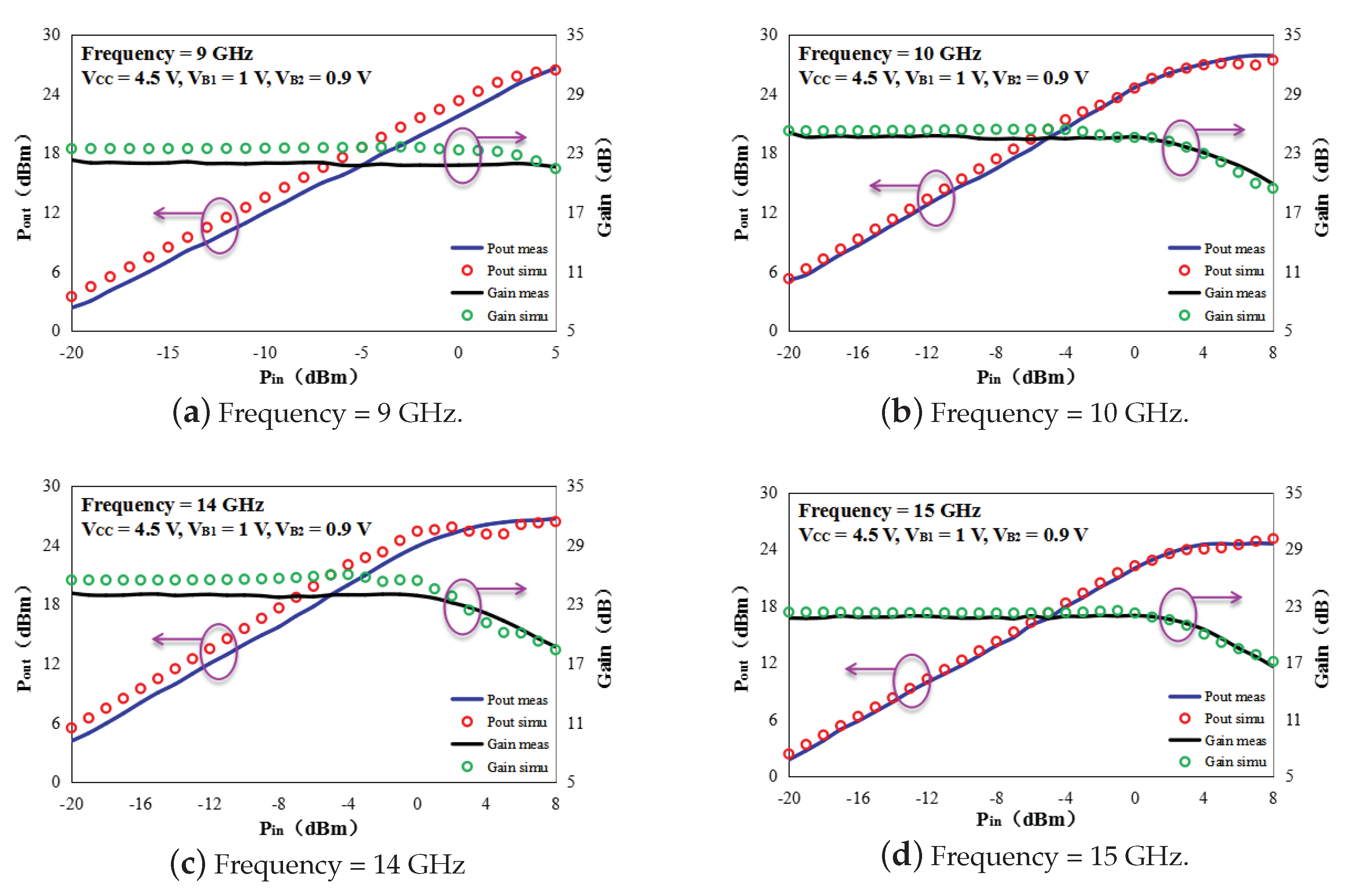
To validate the scalability of the proposed model, a GaAs E-mode pHEMT PA (two-stage, with = 50 m and = 8) has been designed and fabricated. Figure 15 shows the block diagram (left) of the power measurement setup and chip micrograph (right). One-tone large signal measurements were performed at different input driving levels. Figure 16 reveals good matching between the measured and simulated results of the output power for GaAs E-mode pHEMT PA at = 4.5 V, = 1 V, = 0.9 V, and at frequency = 9, 10, 14, and 15 GHz, respectively. Figure 16 indicates the accuracy of the scaled nonlinear model and further verifies the effectiveness of the proposed extraction method.
4. Conclusions
The conventional “ColdFET” method determined and are not accurate in GaAs E-mode pHEMTs. In this letter, we propose an analytical method to extract and directly from S-parameter measurements of the target device. Including the bias dependence of and in small signal modeling has significant impacts on the accuracy of the GaAs E-mode pHEMTs model. The proposed method is verified in both S-parameter simulation and on-wafer measurement, which achieves a good accuracy in a frequency range of 0.5–40 GHz. Furthermore, this paper develops a GaAs E-mode pHEMT PA for verification. The fundamental output power at 9–15 GHz has been measured, which indicates the accuracy of the model and the effectiveness of the proposed extraction method.
Author Contributions
R.D. developed the proposed a new method to extract gate bias-dependent parasitic resistances in GaAs pHEMTs. L.Y. and Z.L. developed the measurement software. R.D. wrote the paper. C.S. and Z.X. supervised the project.
Funding
This work is supported by the National Science and Technology Major Project of the Ministry of Science and Technology of China 2016ZX03001006, NSFC Projects 61731019 and 61674128, by Zhejiang Provincial NSFC Project LY16F010005, and by Major Scientific Project of Zhejiang Lab No. 2018DD0ZX01.
Conflicts of Interest
The authors declare no conflict of interest.
Appendix A. Parameter Sensitivity Calculation
During the parameter extraction, the measurement uncertainties could induce corresponding uncertainties in the model parameters [27]. In order to weigh the model parameters’ uncertainties caused by the measurement uncertainties, the relative sensitivity K in a model parameter x for relative change in S-parameters is defined as [27]:
Then, the relative change in x, which depends on all S-parameters, can be expressed as:
To quantify the measurement uncertainties, the S-parameter deviations are always assumed to be normal-distributed and uncorrelated, and then, the variance in x can be expressed as [27]:
where and represent the S-parameter measurement magnitude and phase relative uncertainties of the Keysight N5247A, respectively. According to the Uncertainty Calculator from Keysight, we can get the relative uncertainty of the N5247A. In the calculation of the model parameter sensitivity and uncertainty estimation, it is necessary to convert the measured S-parameters into Z-parameters first:
where:
Then, it is straightforward to derive all Z-parameter sensitivities by Equation (A1), and the resulting sensitivities are summarized in Table A1.

Table A1.
Z-parameter sensitivities.
In this paper, the parasitic element values (i.e., , , , , , , ) can be derived with high accuracy. According to Equation (A1), the relative sensitivity of , which is related to imag() and imag(), can be expressed as:
The relative sensitivity of A can be expressed as:
Therefore, the and relative sensitivities can be determined by:
Once S-parameters have been measured and parameters have been extracted by the proposed method, the corresponding uncertainties can be estimated.
References
- Lie, D.Y.C.; Mayeda, J.C.; Lopez, J. Highly efficient 5G linear power amplifiers (PA) design challenges. In Proceedings of the 2017 International Symposium on VLSI Design, Automation and Test (VLSI-DAT), Hsinchu, Taiwan, 24–27 April 2017; pp. 1–3. [Google Scholar]
- Cucak, D.; Vasić, M.; García, O.; Oliver, J.A.; Alou, P.; Cobos, J.A.; Wang, A.; Martín-Horcajo, S.; Romero, M.F.; Calle, F. Physics-Based Analytical Model for Input, Output, and Reverse Capacitance of a GaN HEMT With the Field-Plate Structure. IEEE Trans. Power Electron. 2017, 32, 2189–2202. [Google Scholar] [CrossRef]
- Ahsan, S.A.; Ghosh, S.; Khandelwal, S.; Chauhan, Y.S. Physics-Based Multi-Bias RF Large-Signal GaN HEMT Modeling and Parameter Extraction Flow. IEEE J. Electron Devices Soc. 2017, 5, 310–319. [Google Scholar] [CrossRef]
- Na, W.; Liu, W.; Zhu, L.; Feng, F.; Ma, J.; Zhang, Q. Advanced Extrapolation Technique for Neural-Based Microwave Modeling and Design. IEEE Trans. Microw. Theory Tech. 2018, 66, 4397–4418. [Google Scholar] [CrossRef]
- Cai, J.; King, J.; Yu, C.; Liu, J.; Sun, L. Support Vector Regression-Based Behavioral Modeling Technique for RF Power Transistors. IEEE Microw. Wirel. Compon. Lett. 2018, 28, 428–430. [Google Scholar] [CrossRef]
- Alim, M.A.; Rezazadeh, A.A.; Gaquiere, C. Temperature Effect on DC and Equivalent Circuit Parameters of 0.15-μm Gate Length GaN/SiC HEMT for Microwave Applications. IEEE Microw. Wirel. Compon. Lett. 2016, 64, 3483–3491. [Google Scholar]
- Nguyen, T.T.-L.; Kim, S.-D. A gate-width scalable method of parasitic parameter determination for distributed HEMT small-signal equivalent circuit. IEEE. Trans. Microw. Theory Tech. 2013, 61, 3632–3638. [Google Scholar] [CrossRef]
- Gao, J.; Li, X.; Wang, H.; Boeck, G. A new method for determination of parasitic capacitances for PHEMTs. IOP Semicond. Sci. Technol. 2005, 20, 586–591. [Google Scholar] [CrossRef]
- Crupi, G.; Raffo, A.; Vadalà, V.; Vannini, G.; Caddemi, A. A New Study on the Temperature and Bias Dependence of the Kink Effects in S22 and h21 for the GaN HEMT Technology. Electronics 2018, 7, 353. [Google Scholar] [CrossRef]
- Jeon, M.Y.; Kim, B.G.; Jeon, Y.J.; Jeong, Y.H. A technique for extracting small-signal equivalent-circuit elements of HEMTs. IEICE Trans. Electron. 1999, 82, 1968–1976. [Google Scholar]
- Crupi, G.; Schreurs, D.M.; Raffo, A.; Caddemi, A.; Vannini, G. A New Millimeter-Wave Small-Signal Modeling Approach for pHEMTs Accounting for the Output Conductance Time Delay. IEEE. Trans. Microw. Theory Tech. 2008, 56, 741–746. [Google Scholar] [CrossRef]
- Pradeep, D.; Amit, M.; Karmalkar, S. DC Extraction of Gate Bias-Dependent Parasitic Resistances and Channel Mobility in an HEMT. IEEE Electron Device Lett. 2016, 37, 1403–1406. [Google Scholar] [CrossRef]
- Fang, T.; Wang, R.; Xing, H.; Rajan, S.; Jena, D. Effect of Optical Phonon Scattering on the Performance of GaN Transistors. IEEE Electron Device Lett. 2012, 33, 709–711. [Google Scholar] [CrossRef] [Green Version]
- Shinohara, K.; Regan, D.C.; Tang, Y.; Corrion, A.L.; Brown, D.F.; Wong, J.C.; Robinson, J.F.; Fung, H.H.; Schmitz, A.; Oh, T.C.; et al. Scaling of GaN HEMTs and Schottky Diodes for Submillimeter-Wave MMIC Applications. IEEE Trans. Electron Devices 2013, 60, 2982–2996. [Google Scholar] [CrossRef]
- Xing, W.; Liu, Z.; Qiu, H.; Ng, G.I.; Palacios, T. Planar-Nanostrip-Channel InAlN/GaN HEMTs on Si With Improved gm and fT Linearity. IEEE Electron Device Lett. 2017, 38, 619–622. [Google Scholar] [CrossRef]
- Takenaka, I.; Takahashi, S.; Takahashi, H.; Ando, Y.; Kakuta, Y.; Sasaoka, C. Broadband Distortion Cancellation Technique in GaAs HJFET and GaN FET Cascode Amplifier. IEEE Trans. Electron Devices 2014, 61, 3684–3690. [Google Scholar] [CrossRef]
- Geddada, H.M.; Fu, C.; Silva-Martinez, J.; Taylor, S.S. Wide-Band Inductorless Low-Noise Transconductance Amplifiers With High Large-Signal Linearity. IEEE. Trans. Microw. Theory Tech. 2014, 62, 1495–1505. [Google Scholar] [CrossRef]
- Palacios, T.; Chini, A.; Buttari, D.; Heikman, S.; Chakraborty, A.; Keller, S.; DenBaars, S.P.; Mishra, U.K. Use of double-channel heterostructures to improve the access resistance and linearity in GaN-based HEMTs. IEEE Trans. Electron Devices 2006, 53, 562–565. [Google Scholar] [CrossRef]
- Trevisoli, R.; Doria, R.T.; De Souza, M.; Barraud, S.; Vinet, M.; Cassé, M.; Reimbold, G.; Faynot, O.; Ghibaudo, G.; Pavanello, M.A. A New Method for Series Resistance Extraction of Nanometer MOSFETs. IEEE Trans. Electron Devices 2017, 64, 2797–2803. [Google Scholar] [CrossRef]
- DiSanto, D.W.; Bolognesi, C.R. At-Bias Extraction of Access Parasitic Resistances in AlGaN/GaN HEMTs: Impact on Device Linearity and Channel Electron Velocity. IEEE Trans. Electron Devices 2006, 53, 2914–2919. [Google Scholar] [CrossRef]
- Torres-Torres, R.; Murphy-Arteaga, R.; Decoutere, S. MOSFET bias dependent series resistance extraction from RF measurements. Electron. Lett. 2003, 39, 1476–1478. [Google Scholar] [CrossRef]
- Wang, S.; Miao, R.; Peng, S.; Jin, Z. Extracting Small-Signal Model Parameters of Graphene-Based Field-Effect Transistors. Phys. Status Solidi A 2018, 215. [Google Scholar] [CrossRef]
- Crupi, G.; Schreurs, D.M.M.-P. Microwave De-Embedding: From Theory to Application; Academic Press: Oxford, UK, 2013. [Google Scholar]
- Dambrine, G.; Cappy, A.; Heliodore, F.; Playez, E. A new method for determining the FET small-signal equivalent circuit. IEEE. Trans. Microw. Theory Tech. 1988, 36, 1151–1159. [Google Scholar] [CrossRef]
- Crupi, G.; Raffo, A.; Marinkovi’c, Z.; Avolio, G.; Caddemi, A.; Markovi’c, V.; Vannini, G.; Schreurs, D.M.M.-P. An extensive experimental analysis of the kink effects in S22 and h21 for a GaN HEMT. IEEE Trans. Microw. Theory Tech. 2014, 62, 513–520. [Google Scholar] [CrossRef]
- Crupi, G.; Raffo, A.; Caddemi, A.; Vannini, G. Kink Effect in S22 for GaN and GaAs HEMTs. IEEE Microw. Wirel. Compon. Lett. 2015, 25, 301–303. [Google Scholar] [CrossRef]
- Fager, C.; Linner, L.J.P.; Pedro, J.C. Optimal parameter extraction and uncertainty estimation in intrinsic FET small-signal models. IEEE Trans. Microw. Theory Tech. 2002, 50, 2797–2803. [Google Scholar] [CrossRef]
Figure 1.
Small signal equivalent circuits used for extraction. Equivalent circuit of pHEMT in strong inversion at = 0 V (left). Simplified circuit for calculation of (right).
Figure 1.
Small signal equivalent circuits used for extraction. Equivalent circuit of pHEMT in strong inversion at = 0 V (left). Simplified circuit for calculation of (right).

Figure 2.
Measured data and linear regression to calculate and for a pHEMT.

Figure 3.
Measurement setup to perform RF measurements under different bias conditions. Block diagram and photograph for S-parameters (a) and power (b); the inset is the photograph of the 4 × 50μm GaAs E-mode pHEMTs chip. VNA, vector network analyzer.
Figure 3.
Measurement setup to perform RF measurements under different bias conditions. Block diagram and photograph for S-parameters (a) and power (b); the inset is the photograph of the 4 × 50μm GaAs E-mode pHEMTs chip. VNA, vector network analyzer.

Figure 4.
The pHEMT’s small-signal equivalent circuit model shows the extrinsic and intrinsic elements.
Figure 4.
The pHEMT’s small-signal equivalent circuit model shows the extrinsic and intrinsic elements.

Figure 5.
The value of 1/(1 + /) against .

Figure 6.
The value of A against .

Figure 7.
The extracted and against , in which changes about 239% and changes about 270% with from 0.25 V–0.7 V.
Figure 7.
The extracted and against , in which changes about 239% and changes about 270% with from 0.25 V–0.7 V.

Figure 8.
Intrinsic element characteristics of the small-signal equivalent circuit for pHEMT as a function of gate-to-source and drain-to-source voltage (V).
Figure 8.
Intrinsic element characteristics of the small-signal equivalent circuit for pHEMT as a function of gate-to-source and drain-to-source voltage (V).


Figure 9.
Comparison between simulated (symbol) and measured (solid) S-parameters before (red) and after (blue) applying the “open-short” de-embedding procedure for pHEMT at four different bias conditions, where the DUT operates from the pinch-off region to the saturation region.
Figure 9.
Comparison between simulated (symbol) and measured (solid) S-parameters before (red) and after (blue) applying the “open-short” de-embedding procedure for pHEMT at four different bias conditions, where the DUT operates from the pinch-off region to the saturation region.


Figure 10.
The values of for pHEMT at four different bias conditions, where the DUT operates from the pinch-off region to the saturation region.
Figure 10.
The values of for pHEMT at four different bias conditions, where the DUT operates from the pinch-off region to the saturation region.

Figure 11.
Errors between simulated and measured S-parameters.

Figure 12.
The total percentage error between simulated and measured models.

Figure 13.
Comparison between modeled and measured Pout and gain as functions of available input power (Pin) for Vds = 4 V and Vgs = 0.55 V.
Figure 13.
Comparison between modeled and measured Pout and gain as functions of available input power (Pin) for Vds = 4 V and Vgs = 0.55 V.

Figure 14.
Plots of Cgs, Cds, Cgd, Ri, Rgd, gm, and gds with respect to Nf and Wf at Vds = 4 V and Vgs = 0.55 V, respectively.
Figure 14.
Plots of Cgs, Cds, Cgd, Ri, Rgd, gm, and gds with respect to Nf and Wf at Vds = 4 V and Vgs = 0.55 V, respectively.

Figure 15.
Experimental setup to perform power amplifier (PA) measurements under frequency = 9–15 GHz, = 4.5 V, = 1 V, = 0.9 V; block diagram (left) of power; the right is the photograph of PA.
Figure 15.
Experimental setup to perform power amplifier (PA) measurements under frequency = 9–15 GHz, = 4.5 V, = 1 V, = 0.9 V; block diagram (left) of power; the right is the photograph of PA.

Figure 16.
Comparison results of the GaAs E-mode pHEMT PA module.

© 2019 by the authors. Licensee MDPI, Basel, Switzerland. This article is an open access article distributed under the terms and conditions of the Creative Commons Attribution (CC BY) license (http://creativecommons.org/licenses/by/4.0/).
Share and Cite
MDPI and ACS Style
Dang, R.; Yang, L.; Lv, Z.; Song, C.; Xu, Z. A New Method to Extract Gate Bias-Dependent Parasitic Resistances in GaAs pHEMTs. Electronics 2019, 8, 266. https://doi.org/10.3390/electronics8030266
AMA Style
Dang R, Yang L, Lv Z, Song C, Xu Z. A New Method to Extract Gate Bias-Dependent Parasitic Resistances in GaAs pHEMTs. Electronics. 2019; 8(3):266. https://doi.org/10.3390/electronics8030266
Chicago/Turabian StyleDang, Ruirui, Lijie Yang, Zhihao Lv, Chunyi Song, and Zhiwei Xu. 2019. "A New Method to Extract Gate Bias-Dependent Parasitic Resistances in GaAs pHEMTs" Electronics 8, no. 3: 266. https://doi.org/10.3390/electronics8030266
Note that from the first issue of 2016, this journal uses article numbers instead of page numbers. See further details here.