
An Eigenmode Study of Nanoantennas from Terahertz to Optical Frequencies
by
 , , , and
Konstantinos D. Paschaloudis
1 ,
,
Constantinos L. Zekios
2 ,
,
Georgios C. Trichopoulos
3,
Filippos Farmakis
1 and
George A. Kyriacou
1,* 1
Department of Electrical & Computer Engineering, Democritus University of Thrace, 67100 Xanthi, Greece
2
College of Engineering & Computing, Florida International University, Miami, FL 33174, USA
3
School of Electrical, Computer & Energy Engineering, Arizona State University, Tempe, AZ 85287, USA
*
Author to whom correspondence should be addressed.
Electronics 2021, 10(22), 2782; https://doi.org/10.3390/electronics10222782
Submission received: 27 October 2021
/
Revised: 8 November 2021
/
Accepted: 10 November 2021
/
Published: 13 November 2021
(This article belongs to the Special Issue Terahertz Nanoantennas: Design and Applications)
Abstract
:In this work, we present a rigorous full-wave eigenanalysis for the study of nanoantennas operating at both terahertz (THz) (0.1–10 THz), and infrared/optical (10–750 THz) frequency spectrums. The key idea behind this effort is to reveal the physical characteristics of nanoantennas such that we can transfer and apply the state-of-the-art antenna design methodologies from microwaves to terahertz and optics. Extensive attention is given to penetration depth in metals to reveal whether the surface currents are sufficient for the correct characterization of nanoantennas, or the involvement of volume currents is needed. As we show with our analysis, the penetration depth constantly reduces until the region of 200 THz; beyond this point, it shoots up, requiring volume currents for the exact characterization of the corresponding radiating structures. The cases of a terahertz rectangular patch antenna and a plasmonic nanoantenna are modeled, showing in each case the need of surface and volume currents, respectively, for the antenna’s efficient characterization.
1. Introduction
Global mobile data traffic grew in 2017, reaching exabytes per month at the end of 2017 [1]. This tremendous growth in mobile traffic will be 77 exabytes per month by 2022; annually, it is believed to reach almost one zettabyte. By 2025, the number of Internet of Things (IoT) worldwide connected devices is expected to reach 75 billion [2]. This immense expansion of wireless devices and wireless data traffic requires extremely low latencies in the order of 1 ms, real-time data transfer, strong determinism and low-delay jitter in the order of several s [3]. Current communication systems operating at and below 60 GHz are not able to satisfy these high needs [4]. Therefore, the investigation of devices operating at higher frequency bands that can satisfy the need for high data rates, allowing massive connectivity between heterogeneous devices, is needed. To this end, the terahertz (THz) frequency band in the range of 0.1–10 THz, and the infrared and optical spectrum, in the range of 10–750 THz, have recently received noticeable attention in the research community [5,6,7,8,9], appearing as ideal choices for high-speed communication links.
Namely, in 2008, the IEEE suite of standards defined regulatory frameworks over the frequency band ranging between 275 GHz and 3000 GHz [10], which was revised to 802.15.3 in 2014, with the goal of corresponding communication systems being able to achieve data rates in the order of 100 GBps. As also listed by the International Telecommunication Union, the main characteristics of terahertz are as follows [11]: (i) safety—non-ionizing photon energy, (ii) high spectral resolution, (iii) high spatial resolution, (iv) high penetration power, and (v) rapid attenuation in water (the last two characteristics are of less importance, unless more emphasis is put on security in wireless communications). Therefore, these characteristics, together with the much larger bandwidth provided at terahertz frequencies, can satisfy the requirements posed by the exponential growth of wireless data traffic. Terahertz links may offer data rates in the order of 1 TBps, in contrast to mmWave systems that offer links in the order of 10 GBps [4]. Furthermore, terahertz signal propagation offers higher directionality and enables secure communications over highly sensitive links, due to the demand of extremely high gain antennas.
Extensive research has been performed over the last decade on mmWave (e.g., [12,13]), terahertz (e.g., [14,15,16,17,18,19,20,21,22,23]), plasmonic (e.g., [24,25,26,27,28,29]) and optical (e.g., [30,31,32,33,34]) antennas, with the researchers being focused on the following: (a) applying established microwave frequencies techniques at these high frequencies (e.g., [35,36]); (b) identifying suitable materials that are appropriate for design at frequencies over 100 GHz (e.g., [18,23]); or (c) identifying appropriate and low-cost fabrication approaches (e.g., [32,37,38,39]). In this work, we are focused on the first thrust.
Even though microwaves techniques are scalable, the transition from RF-microwaves to optical frequencies needs to be done thoroughly. One of the main aspects that needs to be taken into account is the electromagnetic response of metals at high frequencies. At photonic frequencies, metals behave like lossy dielectrics, and they can be described with the introduction of a complex permittivity [40], whose accurate characterization is challenging due to its frequency dependence. Additionally, in the ultraviolet regime, metals’ permittivity exhibits a relaxation from negative to positive values, while at their plasma resonant frequency of about Hz, it becomes transparent to electromagnetic waves [41]. It is due to this behavior of metals that the penetration of fields and currents requires a particular examination. This challenge was addressed either with the use of parameterized models [42], or by conducting measurements [43]. For instance, in [44], Novotny generalized the linear scaling rule to optical frequencies. In [45], Greffet et al. determined the impedance of a nanoantenna using electric dipole moments. Alù and Engheta et al., with a series of works, described and modeled the features of optical nanoantennas [32,46], tuned their scattering responses through loading [47], and utilized the concept of optical circuit elements [48]. Finally, in [49], Zheng et al. established a natural mode analysis for nanotopologies operating at photonic frequencies.
In this work, we focus on the eigenanalysis of nanoantennas for the frequency range 0.1–750 THz, exploiting the offered insightful view of the studied structures. Utilizing the attained eigensolutions (eigenvalues and corresponding eigenvectors), we are able to determine an in-depth characterization of the nanoantennas’ behavior. Namely, the eigenvalues inform us of the frequency of operation of these antennas, while the eigenvectors identify the modal field and current distributions which indicate the appropriate excitation type. Most importantly, the eigenvectors reveal the behavior of the corresponding materials at these frequencies, and in particular, they inform us about the penetration depth in metals, which serves as the objective of this work. The latter is of critical importance for both theoretical and practical considerations. Namely, from the theoretical point of view, it reveals whether surface currents are sufficient for the characterization of nanoantennas, or the involvement of volume currents is needed. From the practical point of view, it suggests the appropriate thickness of metal needed to maximize the efficiency of structures designed at these frequencies. In this study, we particularly show how the efficiency of a nanoantenna varies, as we take into consideration the appropriate metal thickness. Specifically by utilizing the current flowing in the metallic radiating areas, either surface or volume, we observe that currents penetrating in the metallic regions have a small effect on the efficiency of nanoantennas, suggesting in practical applications the use of thin metallic layers.
The proposed formulation is based on our prior developed eigenvalue technique [50], which is appropriate for the study of any arbitrarily shaped geometry loaded with anisotropic and/or inhomogeneous materials. In what follows, the proposed formulation is demonstrated in Section 2; the penetration depth in metals is investigated in Section 3; and Section 4 cross-examines the results of published studies and those derived from a commercial simulator. Section 5 concludes our work, giving future research directions.
2. Formulation
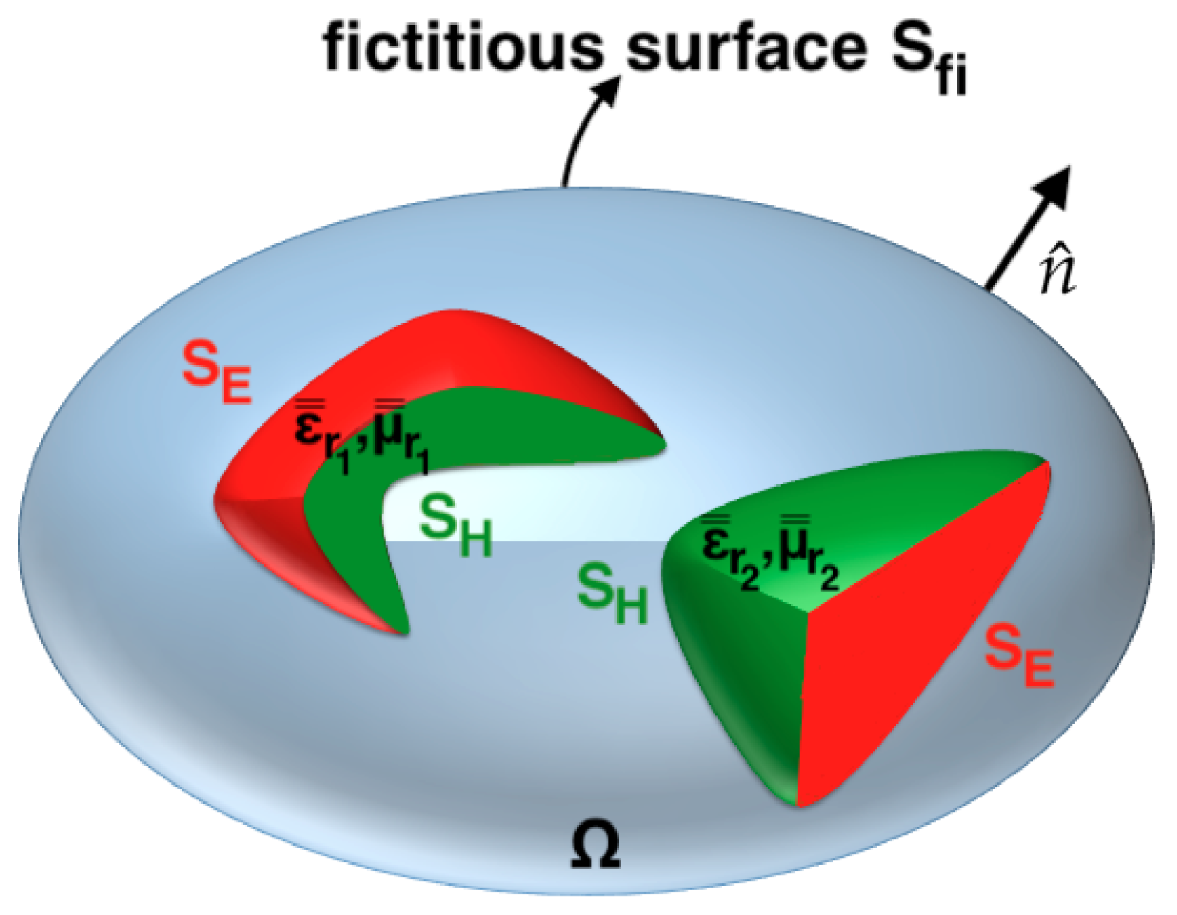
In this work, the finite element method (FEM) is utilized for the eigenanalysis of the studied geometries. Let us assume the source-free, and in general, unbounded domain shown in Figure 1. Absorbing boundary conditions (ABCs) of the first kind are used to apply the radiation condition instead of perfectly matched layers (PMLs), avoiding the well-known spurious Berenger modes [51]. Following our previous work in [52], the resulting formulation is general and able to describe any arbitrarily shaped computational domain, inhomogeneously loaded with, in general, anisotropic material of tensor permittivity (), tensor permeability (), and tensor conductivity (). Perfect electric conductors (PEC), , perfect magnetic conductors (PMC), , and the open-radiating fictitious surface, , where the ABCs are applied, comprise the domain boundary (namely, ). Although the utilized formulation is already given in our previous work [50], let us summarize this approach in the next section for a convenient and self-sustained paper.
2.1. Eigenvalue Problem
Following [53], Maxwell’s differential equations along with the involved boundary conditions, for both the electric and magnetic field, read as follows:
where and are the free space permittivity and permeability, respectively. is the operating resonant frequency, which constitutes the eigenvalue to be sought (i.e., resonant frequency); is the outward unit normal vector defined on the fictitious surface ; and is the resonant wavenumber of free space, which is connected with the circular resonant frequency through the relation , where c is the speed of light.
For sake of convenience, a complex permittivity accounting for both displacement current and conductivity current losses is introduced as follows:
For isotropic media, two alternative representations may be considered. In the first one, all losses are included in a complex dielectric constant as in (2), while in the second one, the total losses are accounted within an equivalent conductivity as follows:
Thus, it is .
It should be noted that these types of losses retain the same form of eigenproblem as the lossless case, apart from the fact that the resulting eigenvalues become complex. On the contrary, the incorporation of ABCs introduces an additional term , besides , rendering the eigenproblem of a polynomial nature.
Eliminating the magnetic field from Maxwell’s equations in (1), the electric field vector wave equation is formed as follows:
Following the standard Galerkin procedure, (4) is written in its weak form as follows [53]:
where is the vector weighting function, is the free space impedance, and i in can be any or all of as appears in (1). The surface integral is defined over the surface of any element. Applying the 1st kind of ABCs [54], (5) takes the following form:
Overall, (7) is general and can be used for the eigenanalysis of any open radiating structure, even for designs operating at photonic frequencies, where the infinite conductivity approach of metals is no more valid. In this case, metals are modeled as frequency-dependent lossy dielectrics with a negative real part of the dielectric constant, making the matrices of (7) also frequency dependent. Therefore, the polynomial nature of the traditional low microwave frequencies system of (7) transforms into a purely non-linear system, increasing its solution complexity. To address this problem, a linearization approach is utilized as discussed in Section 2.2.
2.2. Photonic System Eigenproblem and Its Linearization Approaches
As mentioned above, when metals are modeled in photonic frequencies, they are mathematically described as frequency-dependent dielectric materials, transforming the polynomial eigenvalue problem of (7) (we assume here that the dielectric materials we use are not frequency dependent, and therefore at low microwave frequencies, (7) is only of polynomial type since S and M have no frequency dependence; note that the wavenumber () is the eigenvalue of the problem under solution) to a non-linear eigenvalue problem. To address this non-linearity, a linearization approach is needed. Two different approaches are used: (a) the recursive formulation, and (b) the auxiliary field-based formulation.
2.2.1. Recursive Formulation
In the first approach, an iterative process is introduced, the details of which can be found in our previous work [50]. For reasons of completeness, we only give here a brief description of this method.
We start by setting an initial eigenvalue that corresponds to the expected eigenmode. Based on this value, the electric permittivity for all the metals is determined, using the appropriate model (in this work, we use the Lorentz–Drude model [42]), and the mass matrix is constructed, obtaining an eigenproblem of the form of (20). We solve this problem and we obtain a vector group of complex resonant eigenfrequencies represented as . An updated mass matrix is constructed based on , and a new eigenproblem of (20) form is attained and solved, yielding a new vector group of complex resonant eigenfrequencies, . The process continues for a number of iterations, , obtaining . It is terminated when two consecutive estimations of the eigenvalue change less than a prescribed error tolerance. Even though this approach is effective, transforming the non-linear eigenproblem to a regular polynomial eigenproblem is very time consuming. Note that the obtained eigenproblem needs to be solved multiple times for each eigenvalue to acquire the desired relative error. Therefore, this linearization approach is efficient only when a small number of eigenvalues is desired.
2.2.2. Auxiliary Field-Based Formulation
When a significantly larger number of eigenvalues is sought, we follow a different approach, recently introduced in both finite difference time domain [55,56] and finite difference [57], finite element [58], and frequency domain simulations for dispersive media. In this second method, a “hidden” auxiliary field is introduced by considering non-magnetic mediums whose permittivities can be modeled by a standard pole Lorentz–Drude relationship [57,59]:
In (11), M is the number of oscillators (poles) with frequency , is the oscillation strength, and is the relaxation rate, which describes the effective electron scattering rate . The parameter stands for the volume plasma frequency, where N is the electron’s density, e is the electron’s charge, and m is the effective mass of the electron. Finally, the parameter is called instantaneous or high-frequency relative permittivity, and it accounts for the net contribution from the positive ion cores. The typical values for for the utilized metals range between 1 and 10, depending on the intraband response. For ideal free electron gas, it takes the value , which is a common choice in many published works.
Let us consider the case of a single-pole Lorentz–Drude model, and introduce two auxiliary fields as follows [59]:
where is the polarization field, which is correlated with the electron’s concentration as (: position), and is the current density. Thus, the basic equations of motion for the electromagnetic field in a dispersive (non-magnetic) medium are as follows [57]:
Combining (13a) with (13b) and (13c) with (13d), we obtain a system of coupled wave equations involving the electric field and the electric polarization as follows:
In matrix notation, (14) reads as follows:
The system (15) refers to a polynomial eigenvalue problem. The aforementioned approach can be extended for the case of the multiple-pole Lorentz–Drude model by simply increasing the number of auxiliary fields, namely, taking into account more terms from the expansion in (11). Eliminating the frequency of the pole (), the Lorentz–Drude model (11) reduces to the simple free-electron Drude model. The latter requires the introduction of a single auxiliary field to convert the non-linear eigenproblem into a linear one.
Applying the standard Galerkin procedure and using the 1st kind of ABCs, the weak formulation of system (15) becomes the following [53]:
The stiffness , mass , and radiation matrices are defined in (8)–(10), respectively, while the auxiliary field–related matrices read as follows:
The system (16) can be rewritten in a more compact form as follows:
As it turns out, after the linearization procedure system, (18) has the same form with (7); therefore, both can be solved following the same approach as described in Section 2.3 below.
2.3. Polynomial Linearization
Formulation (7) is of the second-order polynomial form with respect to the eigenvalue . Thus, the incorporation of a linearization procedure is needed in order to solve this eigenproblem. A symmetric linearization approach is utilized herein, taking advantage of the symmetric nature of the involved matrices.
By setting , (7) reads as a single standard quadrature problem with a characteristic polynomial:
Defining an auxiliary vector , where q refers to the “seeding” vector, and, therefore, using the eigenvector transformation of the form , (7) becomes the following [60]:
As it occurs, (20) is a linear generalized eigenvalue problem, where its eigenvalue corresponds to the complex wavenumber , with . To solve this problem, the Arnoldi shift and invert algorithm is utilized [61]. After the solution of our system, the resonant frequency of the structure is derived, using the real part of the wavenumber as , while the imaginary part is used to determine the corresponding quality factor as .
3. Investigation of Field Penetration in Metals
A key aspect on the characterization of antennas’ performance at terahertz and optical regimes is the skin depth of the metallic regions. The skin depth depends on the frequency of operation and the conductivity of the material. Its value can be analytically calculated as follows [62]:
where , and is the complex propagation constant of an incident plane wave given as follows:
Considering the definition of (3), the skin depth for isotropic metals can be written in terms of either an effective conductivity, or the imaginary part of the complex dielectric constant as follows:
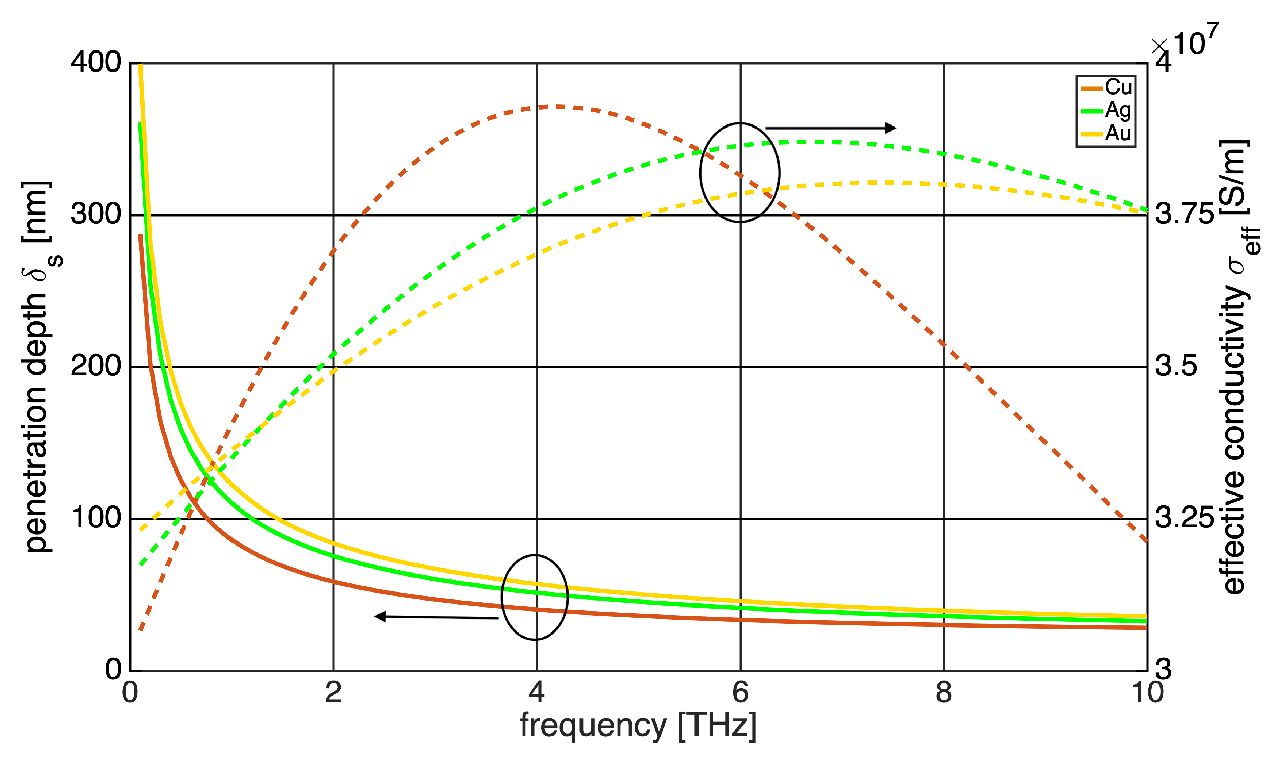
The values of and (see (2)) are calculated either using the Drude or single-pole Lorentz–Drude model. Both models give the same distributions in the terahertz frequency spectrum, as the intraband transition of electron is the dominant mechanism, and the contribution of the interband counterpart is negligible [42]. Note that in this study, all modeled structures are non-magnetic; therefore, is omitted.
As discussed in the introduction, the goal of this work is to investigate whether the surface currents are sufficient for the correct characterization of nanoantennas, or the involvement of volume currents is needed. To do so, we study the penetration depth in conductive regions consisting of copper (Cu), silver (Ag), and gold (Au) for the two frequency ranges of interest: (a) 0.1–10 THz, and (b) 10–750 THz. Note that copper and silver are extensively used at terahertz frequencies [14,15,19,21,22,23], while gold (Au) films are mostly used in photonic and plasmonic structures [24,26,28,31], even though it appears in some works at a lower terahertz, especially in sub-terahertz applications, where gold films are a common choice [20]. The question to be addressed is whether for practically utilized metallic film thicknesses, the electric field penetrates to some significant depth, where the corresponding current density must be treated as a volume distribution. Otherwise, if the current epidermal nature prevails, this distribution can be considered to be a surface one (infinitely thin). In the latter case, the rules and approaches established in the microwave and millimeter wave regimes can be directly applied.
3.1. Penetration Depth at 0.1–10 THz
First, we start investigating the penetration depth in the 0.1–10 THz frequency range. As an example, we use a typical patch antenna. The typical thickness (t) of metallic portions for a patch antenna (i.e., the metallic isle on the top and its ground plane) varies from 0.25 m to 0.5 m [21,22], or in some thicker alternatives from 40 m to 50 m [14,15], while known substrate materials like Rogers RO3010, −3006, and −3003 are also made with m [63]. (For metal thicknesses below 9 m, lithographic techniques are used (e.g., electron beam lithography (EBL) and focused ion beam (FIB) milling) [64].) The specific thickness is selected based on the maximum (nominal) current density to be encountered (thus, the structure’s operating power) and the specified mechanical rigidity [65]. The penetration depth in metals is inversely proportional with frequency when the metal’s conductivity and dielectric constant vary according to the Drude model (11). Thus, as frequency increases, the penetration depth decreases as depicted in Figure 2. Therefore, the penetration depth is significantly smaller than the typical metal thickness at the high end of the observable frequency range, and the skin effect met in a low-microwave (i.e., GHz) patch antenna is still valid at these frequencies. In this case, metals can still be considered perfect electric conductors, and the antenna behavior can be characterized by surface currents flowing on the surface of the patch.
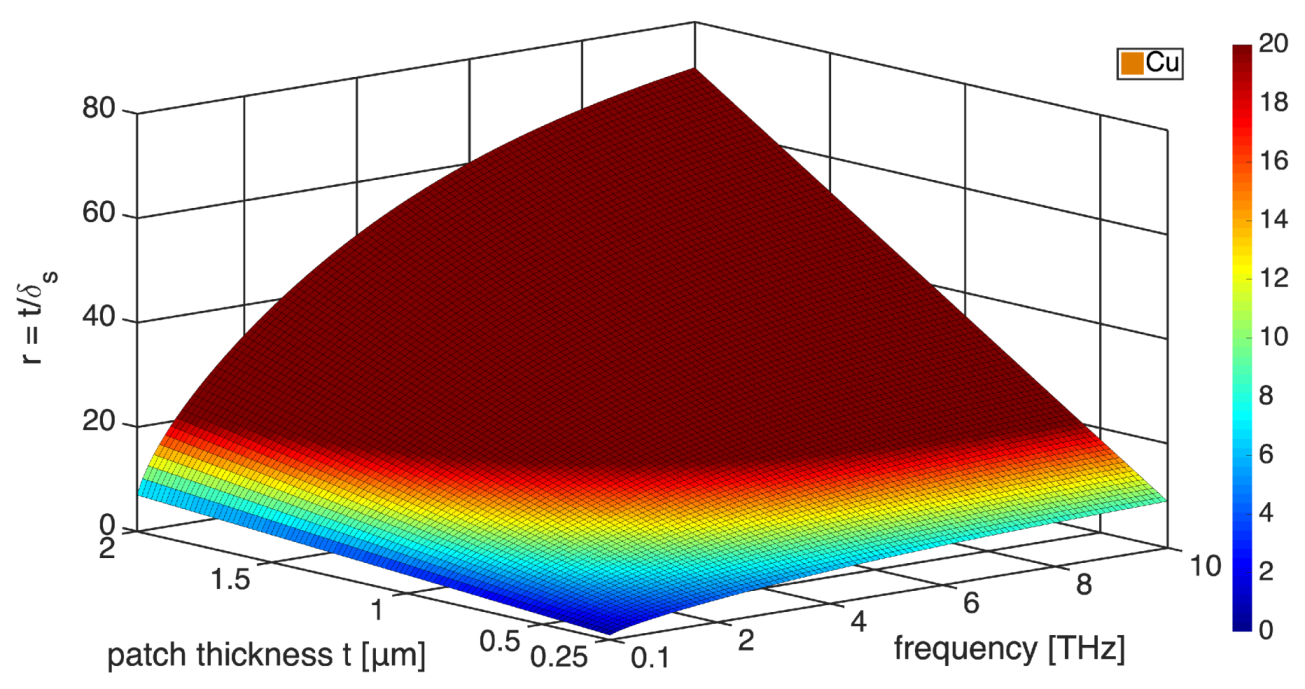
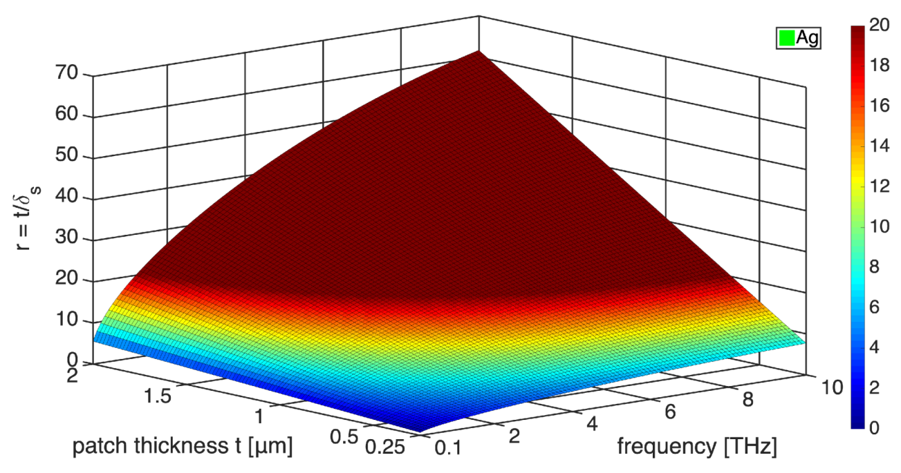
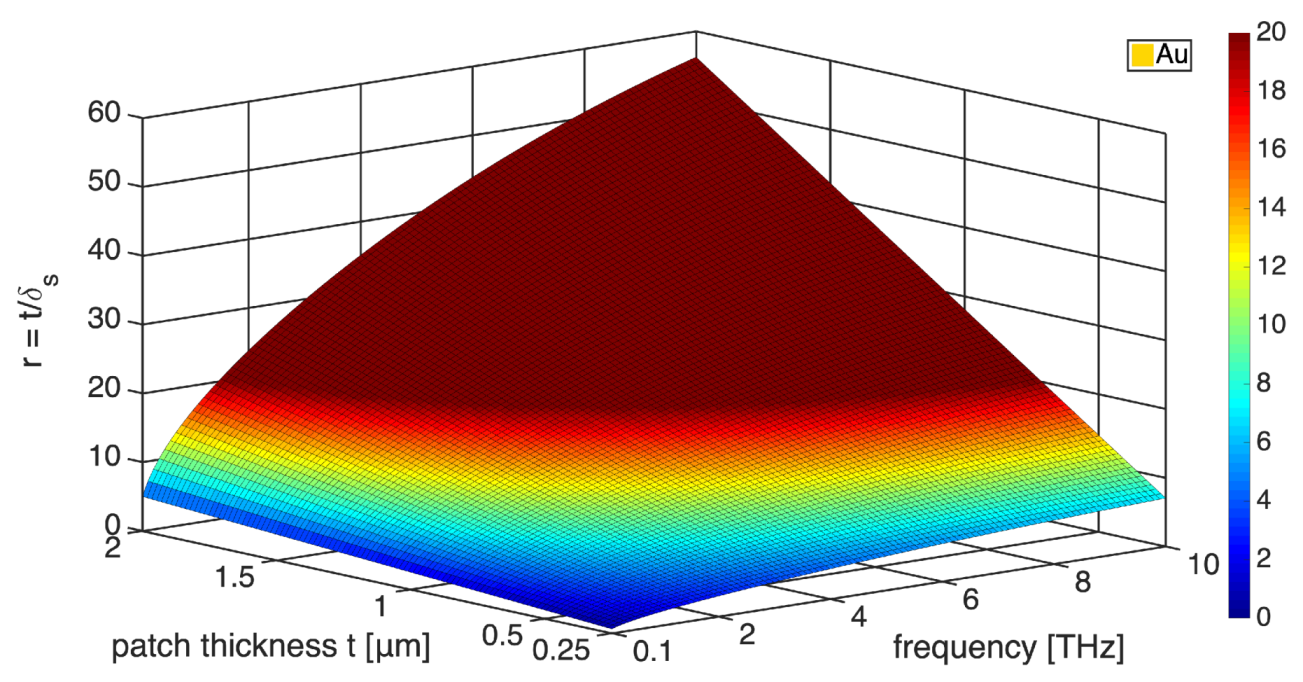
Although surface currents seem to be sufficient for antennas characterization at the 0.1–10 THz frequency range, when the metallic layers are thick, it might not be the case for thicknesses below 2 m. Figure 3, Figure 4 and Figure 5 present a 3D plot of the ratio of the metal thickness m to the penetration depth , at the terahertz frequency range of 0.1–10 THz for the cases of Cu, Ag, and Au, respectively. It is clearly evident in these plots that patch antennas, whose metallic layers thicknesses are in the order of micrometers, exhibit penetration depths of several orders of magnitude lower than the metal thickness. Only for the frequency range below 2 THz, the penetration depth remains comparable to the thickness of the metallic layers. Therefore, for cases of metal thickness m and for frequencies below 2 THz, volume currents must be used to appropriately characterize the corresponding antennas. A recent report on the design and simulation of terahertz-integrated antennas [66] stated that the increase in conductor thickness results in better radiation efficiency. Thus, in practical situations, thicker metallic claddings are preferred, as was also shown in [67] with a microstrip antenna array operating at 0.1 THz.
3.2. Penetration Depth at 10–750 THz
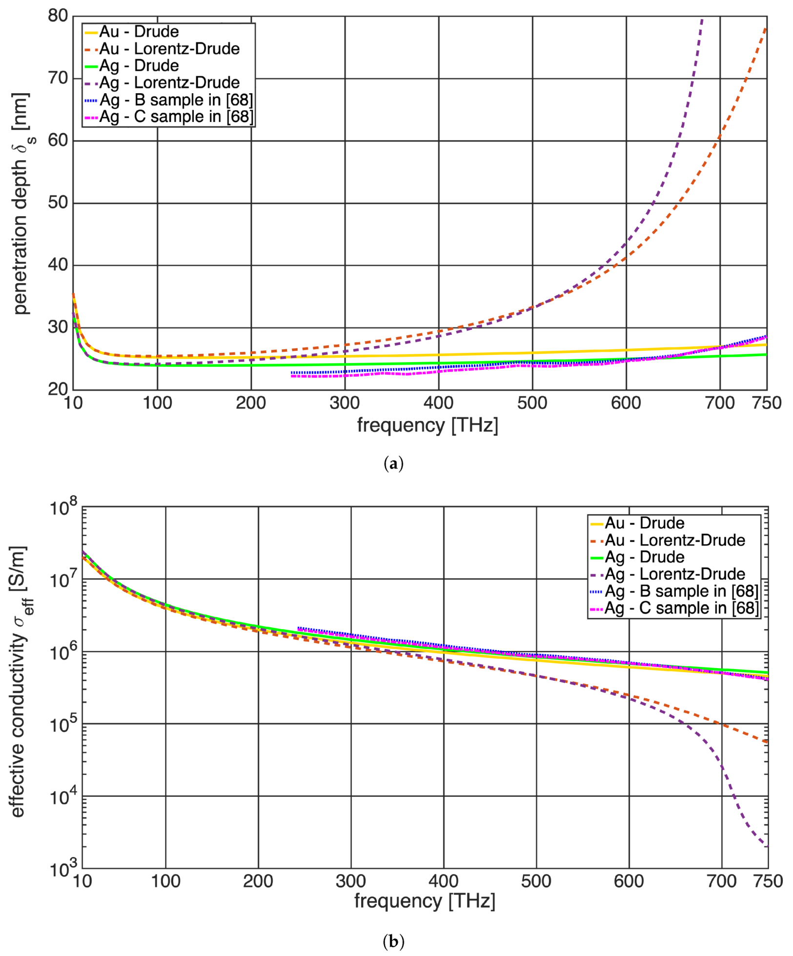
In our second study, we investigate the penetration depth in metals for the frequency range of 10–750 THz. Only the penetration depth in Ag and Au is studied, as Cu is not met in optical configurations. Figure 6 depicts the penetration depth in nm and the effective conductivity in S/m for these two cases, utilizing both Drude and Lorentz–Drude models as well as the results derived from the measurements of two silver samples [68]. As expected, the penetration depth responses are different for the two models since the contribution of the intraband transition of electron becomes comparable with the interband counterpart [42]. However, the penetration depth of Ag based on measurements has a response closer to the simple Drude model.
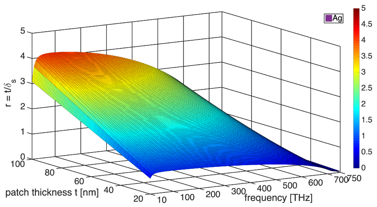
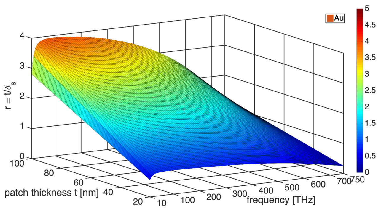
Regarding the thickness of the metallic portions for optical nanoantennas, it varies at nm [24,25,69,70]. (A thickness of nm was used for a gold patch in an experimental setup in [25], while thicknesses for both silver and gold patches at nm are found in [24,69,70]). See in Figure 6a how the penetration depth is comparable to the thickness of the nanoantennas’ metallic parts, especially when the interband contribution is taken into account through the Lorentz–Drude model. This is also shown in Figure 7 and Figure 8, which present a 3D plot of the ratio of the metal thickness nm to the penetration depth , , at the frequency range of 10–750 THz. The same situation also exists when the simple Drude model is utilized, due to the small thickness of the metallic portions used at high terahertz frequencies. Therefore, the displacement and polarization currents, flowing along and inside the nanoantenna, become dominant, indicating that the antenna’s characterization should be done through the study of a volume current distribution.
4. Numerical Results
The cases of a terahertz rectangular patch antenna and a plasmonic nanoantenna are modeled in this Results section. As proved next, the surface currents can sufficiently characterize the terahertz patch antenna, while volume currents are needed for the plasmonic nanoantenna. An in depth study is performed for the latter, showing the importance of metal thickness, as it affects the radiation efficiency of the structure.
4.1. Rectangular Patch Antenna at 0.1–3 THz
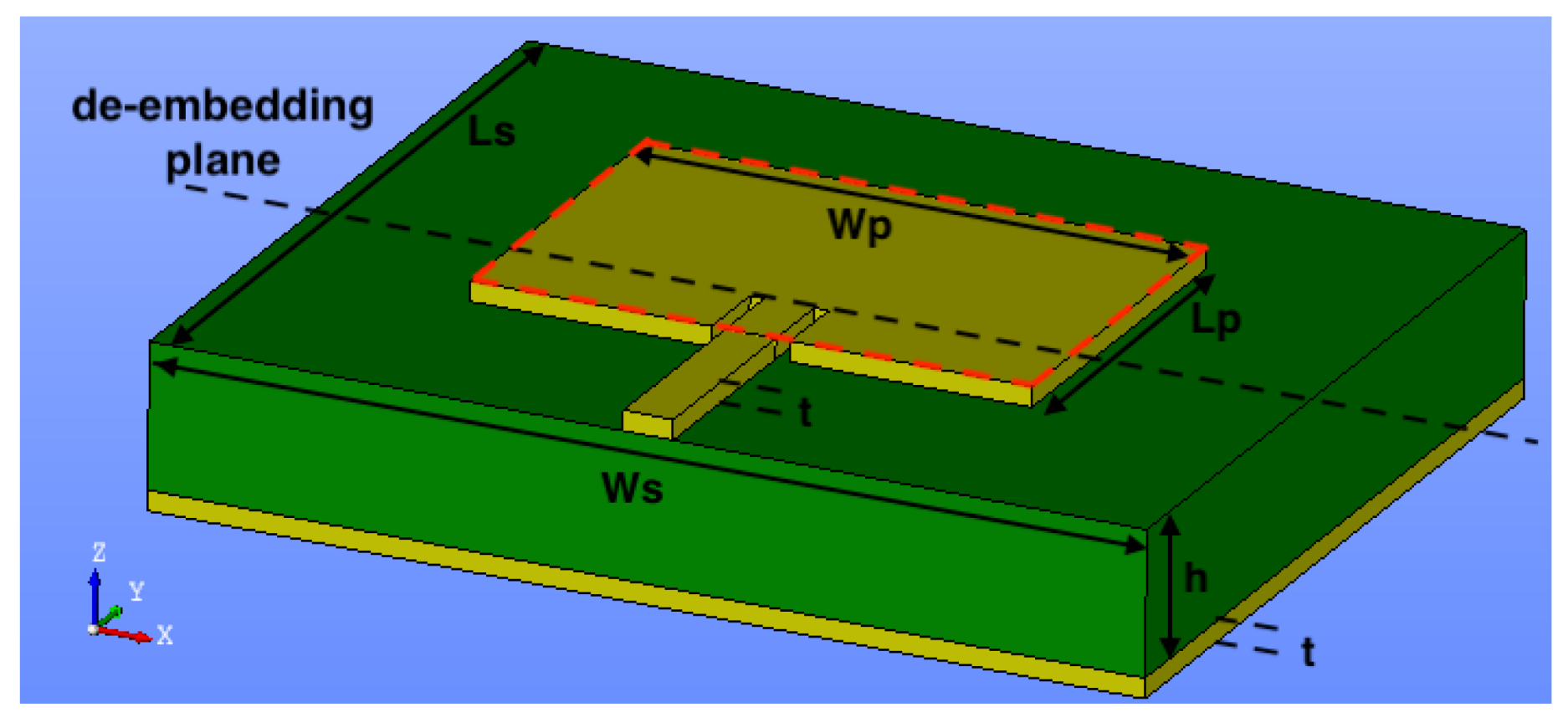
Let us examine the case of the simple terahertz rectangular patch antenna depicted in Figure 9 with m, m, m, m, m, m, designed on the transparent polyimide substrate material met in terahertz applications [22] with a dielectric constant of . (Since we investigate the design and performance of a terahertz patch antenna, the substrate material is assumed to be lossless, and thus, .)
The eigenproblem of the terahertz patch antenna without the feeding line (only the rectangular patch denoted by the red line in Figure 9, the substrate and the ground plane) is solved with the recursive formulation (Section 2.2.1), utilizing a fixed value of silver’s permittivity, determined with the Drude model (11) at 1 THz. The first 10 eigensolutions are obtained and tabulated in the second column of Table 1. To avoid any misunderstanding, recall that eigenmodes are independent of any excitation. However, their modal current (magnetic field) or voltage (electric field) distribution may identify the appropriate position of the excitation along with which the quantity, current or voltage can be maximized at the corresponding resonance. In turn, these resonances are characterized as parallel (maximum voltage at the feed) and series (maximum current at the feed) ones.
The eigenvalues of the terahertz patch antenna are cross examined with those (third column in Table 1) resulting from the eigenanalysis of the same structure, but utilizing the auxiliary field-based formulation (Section 2.2.2). The small deviations of the average order of between the resonant frequencies (real part of eigenvalues), resulting from the two formulations, are due to the different approach used for characterizing the metallic layers. The first approach (recursive formulation in Section 2.2.1) uses a constant permittivity value for the characterization of metals throughout the whole frequency spectrum, while the second one (auxiliary field-based formulation in Section 2.2.2) changes the permittivity of metallic regions according to the attained resonant frequency. It should be noted that CST also uses a fixed permittivity for metals at low terahertz frequencies (below 150 THz) [71].
Closely examining Table 1, one may encounter a plethora of nearby located resonant frequencies. This is unexpected for patch antennas and may lead to the suspicion of pseudo-spurious eigensolutions. However, the experience in printed antenna eigenproblems (especially in their characteristic modes analysis) reveals that the majority of the obtained resonances are due to the finite grounded dielectric substrate. From this point of view, two separate families of eigensolutions are expected: (a) one due to the finite grounded substrate (in the absence of the patch radiator), and (b) one generated by the patch radiator itself (e.g., a patch on infinite substrate). Therefore, the observed eigensolutions for the patch antenna of Figure 9 are the results of mode coupling between these two families. In order to shed light to these phenomena, an eigenanalysis is performed, obtaining the eigensolutions of the structure shown in Figure 9 in the absence of the patch and the feeding line. Therefore, eigenfrequencies () shown in Table 1 are the pure resonances of our finite substrate, which, as expected, are slightly shifted to the corresponding eigenfrequecies when the patch radiator is present (see in Table 1). It is next proved that for these substrate modes, the eigencurrents have strong intensity on the ground plane and are negligible on the patch radiator. On the contrary, eigenfrequencies () of the patch radiator are expected to have eigencurrents with strong intensity on the patch itself.
The presence of the excitation, especially the inset feed of Figure 9 modifies the metallic patch geometry and is expected to shift its resonant frequencies. For this purpose, the eigenproblem of our THz patch antenna as depicted in Figure 9 (with the presence of the feeding line) is solved once again, utilizing the auxiliary field–based formulation. The eigenvalues of the latter are listed in Table 1 as . As it can be seen from them, the presence of the feeding line not only causes a subtle change in the eigenfrequencies (compared to in Table 1), but more importantly, it creates a new eigensolution No. as it appears in Table 1. Notably, by carefully observing the patch antenna in Figure 9, the slots of the inset-feed are expected to force the directed current density () to flow around them, thus increasing their resonant path. Although these modes cannot be excited by this feed, their resonant frequency will be shifted downwards. This is observed, for instance, for modes () of the last column of Table 1.
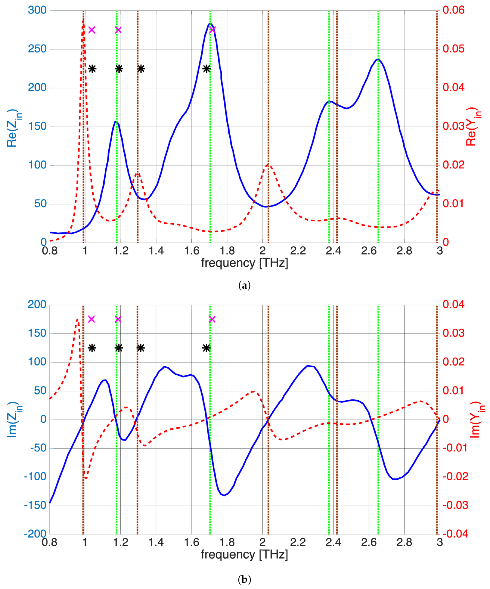
To prove the validity of the eigenanalysis, Figure 10 presents the real and imaginary parts of both input impedance and input admittance versus the frequency for our terahertz rectangular patch antenna as simulated in CST Microwave Studio [71]. It is by now well established that the true nature of the patch radiator is revealed at its actual input, identified at the feeding line-patch interconnection. This is usually obtained through the de-embedding approach, which is also available in all commercial simulators. Observing the de-embedded input impedance in Figure 10, one may identify multiple resonances at frequencies THz, where , with an average value of . The first two resonances are identified in Table 1 as modes and , while the others fall outside the region spanned by the eigenanalysis. Similarly, multiple resonances at frequencies THz, where , are observed in Figure 10, with an average value of S. Likewise, the first two resonances correspond to modes and of Table 1. All the aforementioned resonances can be identified as different modes.
It is important to realize that the resonances appearing in the diagram of versus frequency (blue solid line in Figure 10a) are only a subset of the supported modes; namely, these are only modes excited by the specific feed. Additionally, the commonly utilized operating modes in patch antennas are only the parallel resonances appearing at (vertical green dotted lines). However, there are always series resonances between successive parallel modes, where () (vertical brown dotted lines) as seen in Figure 10a. These series modes are found to be inappropriate for operating–exciting a patch antenna. Hence, the eigenanalysis provides a plethora of antenna modes (see Table 1 besides the substrate modes), which can be discriminated as series and parallel resonances, while only a subset of them can be excited by the feed utilized in Figure 9.
As explained above, it is important to illustrate the modal current distributions in order to identify the position and the type of possible excitations. Surface currents result from the so-called internal magnetic field (below the patch) as . The eigenvoltage distributions, defined between the patch and the ground plane, can be also illustrated. This can be easily done since . Then, the voltage is computed as , which for a thin substrate of height h the component is nearly homogeneous in the z-direction; thus, . Nevertheless, since the parallel resonances are only considered operating modes, the series resonances are neglected, which can be simply identified as those whose current distribution at the feed is maximal.
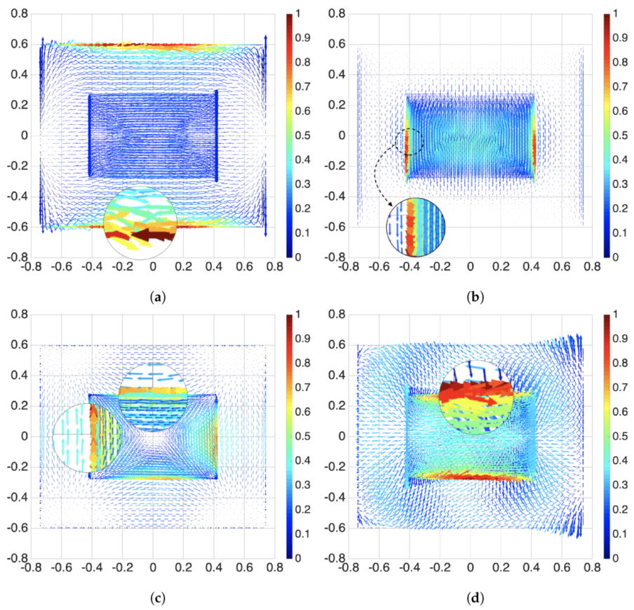
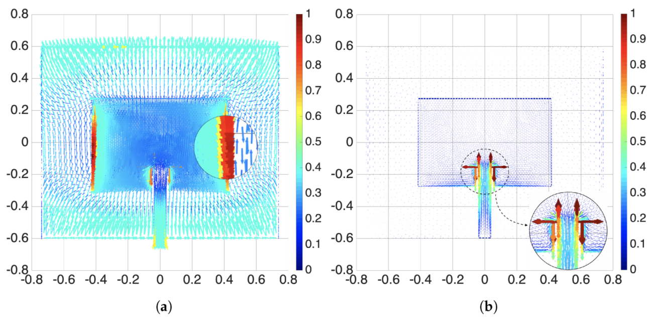
The eigencurrent distribution of mode Nos. 1, 4, 5, and 10—see column in Table 1—flowing upon the top surface of the patch (top isle) and the ground layer are illustrated in Figure 11. The surface current distribution of mode (see Figure 11a) clearly reveals that this is a non-radiating finite substrate mode since its current density is higher on the ground plane rather than on the patch radiator. In turn, the surface current distributions of mode Nos. 4, 5, and 10 correspond to the , , and radiating patch modes, respectively (see Figure 11b–d). Namely, the current distribution of the dominant mode (Figure 11b) is the same with the one observed in the source-driven CST analysis of a typical microwave rectangular patch antenna. Regarding the other (such as No. ) mode distributions of our patch, they cannot be computed with this source-driven CST analysis since these modes cannot be excited with the specific feeding line. Figure 12 shows the eigencurrent distributions for mode Nos. 3 and 6—column in Table 1—where the modification of distributions due to the presence of the feeding line is clearly evident. Special attention should be given to the current distribution of mode (Figure 12b), which represents a series resonance (maximum current at the feed) and clearly reveals why series resonances are inappropriate for operating–exciting a patch antenna. An insight is offered by Figure 12 regarding the affected current density components. Clearly, the directed current (), which is parallel to the inset feed slots, is negligibly affected, and thus, without any noticeable shift in the resonant frequencies of the corresponding mode Nos. 4, 5, and 10. On the contrary, modes with dominant directed currents, which are normal to those slots, are strongly affected or even revealed by the corresponding eigenanalysis ( in Table 1).
Overall, it is justified, herein, that the behavior of a patch antenna operating at terahertz frequencies can be once again characterized by the surface currents flowing on its metallic layer.
4.2. Plasmonic Nanoantenna at 400–600 THz
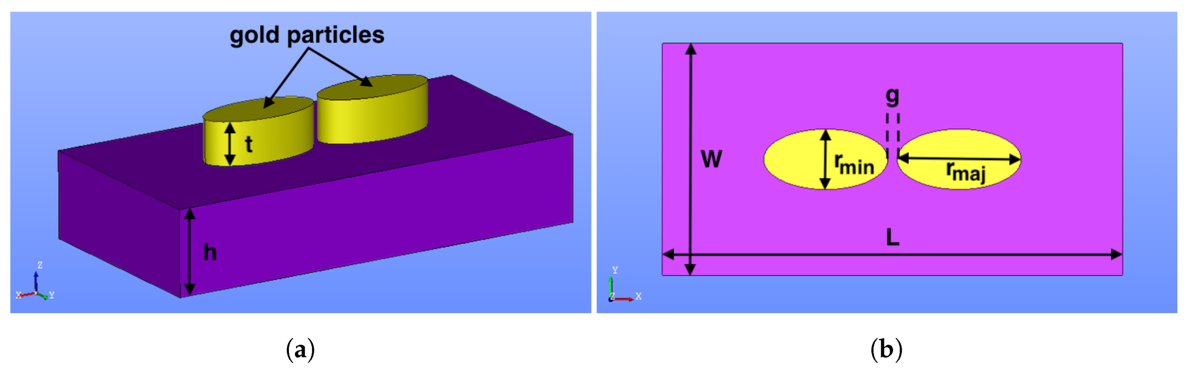
In the second example, we study the plasmonic nanoantenna shown in Figure 13 introduced by Liu et al. [24]. This structure consists of two elliptical cylinder shape gold nanoparticles placed upon a quartz substrate with geometrical characteristics as depicted in Figure 13. The thickness of the particles is nm each and their in-between gap is nm, while their major and minor axes are nm and nm, respectively.
Table 2 presents 10 eigenvalues and the corresponding resonant wavelengths of this plasmonic nanoantenna in the frequency range of interest. The same approach as that for the terahertz patch antenna of the previous section is utilized. Hence, the eigenanalysis using the auxiliary field–based formulation (Section 2.2.2) is first carried out for the whole antenna of Figure 13, while this is repeated afterward in the absence of the gold nanoparticles. These eigenvalues are cross examined among them, where it is clearly revealed that only eigenvalues Nos. 3 and 4 are related with the nanoparticles (antenna) modes, while the rest correspond to substrate modes. The electric current density () defined in (12b) includes both the conduction current () and the displacement current () through the complex permittivity (2) or (11) according to (12b):
On the contrary, at lower frequencies, metals behave as perfect electric conductors (PEC), where the tangential electric field vanishes, leading to the assumption of the surface current density . The resulting current distributions are estimated and plotted in Figure 14.
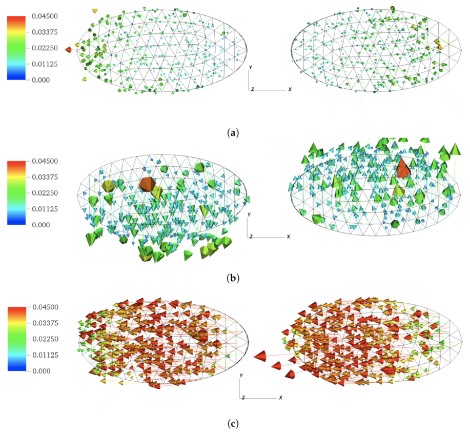
The two antenna modes () are compared in terms of their eigencurrents and against an indicative substrate mode (1) as illustrated in Figure 14. A close examination of Figure 14c shows that mode No. 4 represents the usual dipole antenna, as its current flows parallel to the long axis of the ellipse and toward the same direction. Conversely, the antenna mode No. 3 exhibits a surprising, strange behavior since its current is normal to the major axis of the ellipse having opposite directions. As these currents are very close, they are expected to yield negligible radiation. Moreover, Figure 14a shows the electric current density flowing upon the gold particles for the substrate mode , where its weak intensity, due to the fact that it is a non-radiating mode, is clearly evident. Namely, this substrate mode exhibits a dipole-like current, being parallel to the ellipse’s major axis and flowing in the same direction, but with its intensity being zero at the two edges of the gap. Hence, this mode cannot be excited by the usual, for instance, gap voltage in transmit function, while a detector placed across the gap will receive no response in the receive function. Overall, the eigenanalysis revealed that the useful antenna mode is illustrated in Figure 14c, exhibiting the expected dipolar polarization and resonating at a wavelength of 632 nm, which is in accordance with the original study performed in [24].
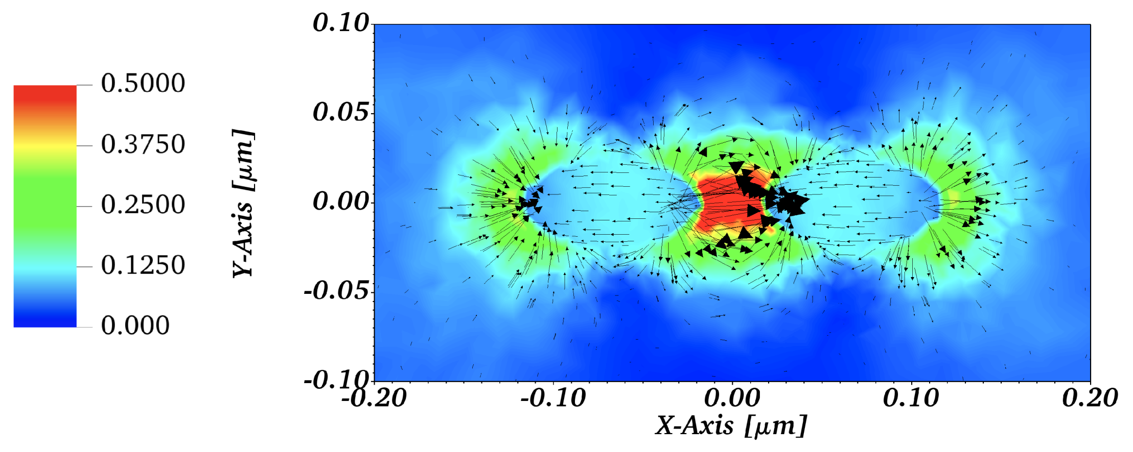
Figure 15 shows the real part of the eigenvector at an view 20 nm above the substrate (at the middle-plane crossing the particles) at a wavelength of nm (eigenvalue ). In this wavelength, the high enhancement of the local field in the gap between the two gold particles, a common characteristic of nanoantenna structures [24], is clearly evident. Additionally, the electric field vector directions reveal the dipolar nature of mode (4).
As stated throughout this paper, a major task of this work is to examine the current distribution over the entire volume of the nanoantenna in order to gain an insight into their radiation mechanism. For this purpose, a side view of the antenna mode distributions for the electric current density is shown in Figure 16. It is clear that the current flows inside the gold nanoparticles, and is not restricted on the surface as happens to antennas operating at low-microwaves (below 100 GHz). Hence, the correct characterization of a nanoantenna operating at optical frequencies needs the use of volume current. Moreover, the current flow is mainly concentrated at the lower interface of the gold layers and the substrate, and is parallel to the substrate for operation at antenna modes (Figure 16b,c). On the contrary, the current flow is concentrated at the top side corner of the gold particles and is normal to the substrate for operation at substrate mode (Figure 16a).
To show the effect of volume currents, in the following subsection, the radiation efficiency of this plasmonic nanoantenna is evaluated as a function of the current’s penetration depth in the gold nanoparticles.
Plasmonic Nanoantenna Radiation Efficiency—Volume Current
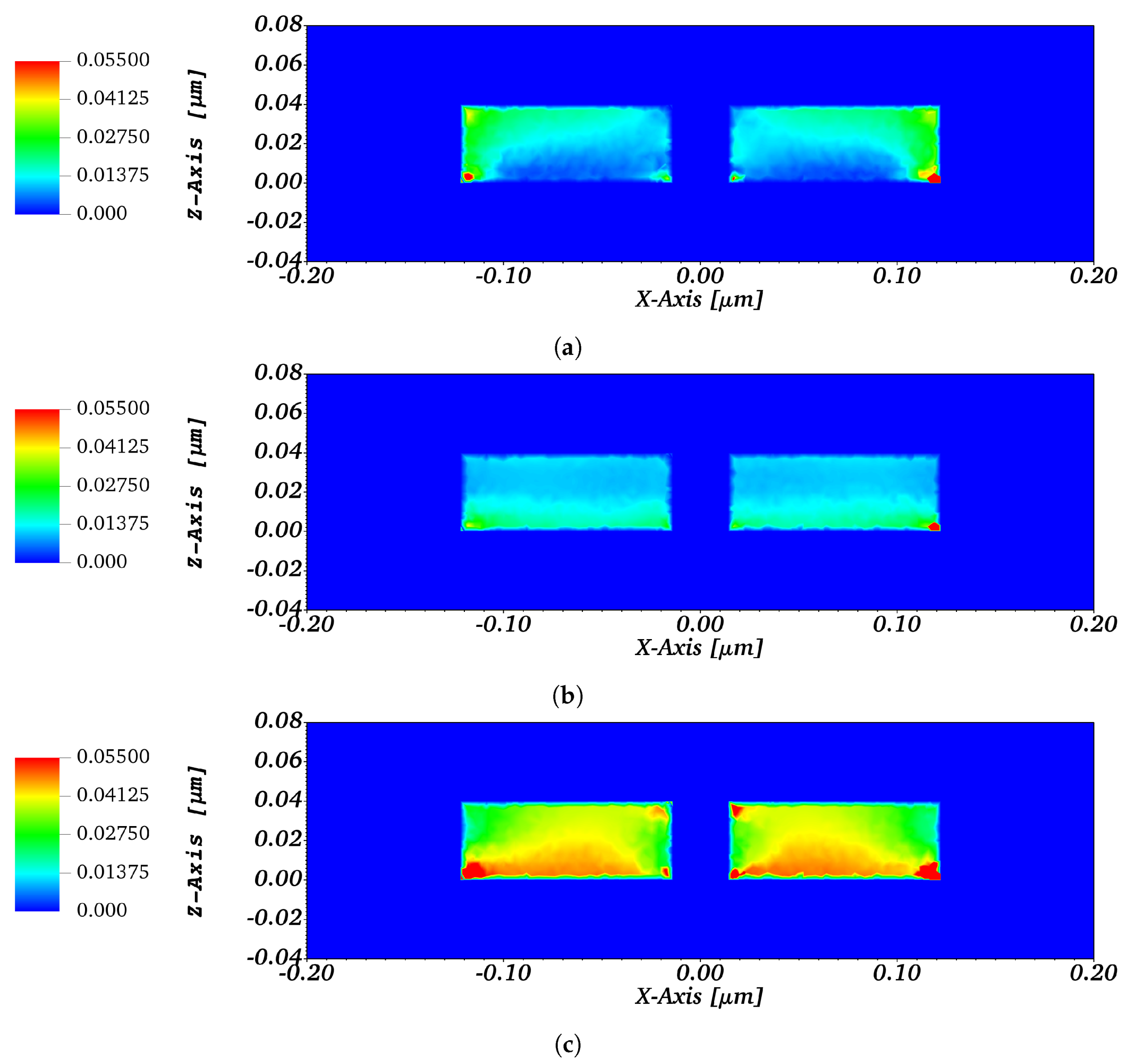
As shown in Section 3.2 for the plasmonic nanoantenna of Figure 13, at frequencies of operation above 200 THz, the penetration depth in metals is significant compared to the metal’s thickness. Notably, for the three different cases, at nm, nm and nm, the electric current penetrates in the gold particles, forming the corresponding spatial mode distributions (Figure 16). In order to reveal the effect of the volume currents, the nanoantenna’s radiation efficiency, , is evaluated according to [72] for different thicknesses of metal and for the two antenna modes. Namely, the gold nanoparticles of the plasmonic nanoantenna is divided into three layers (Figure 17): (i) one bottom layer of thickness nm interfacing the substrate, (ii) a middle layer above the first one of thickness nm, and (iii) a third top layer of thickness nm. For each case, the radiated power is computed utilizing the corresponding volume eigencurrents [72]:
Explicitly, refers to the total dissipated power, whose real part represents the radiation power , while its imaginary part, the Joule losses .
Assuming the same input power, , for all the three cases, the corresponding radiation efficiencies are estimated [72], , where corresponds to the three different layers (bottom (red), middle (green), and top (yellow) as shown in Figure 17). Note that all dielectrics are assumed to be lossless, and any other source of radiated power other than the two gold nanoparticles is omitted. Table 3 lists the radiation efficiency and the corresponding contribution to the radiated power for all the different cases. One may observe that the currents flowing at the bottom layer (red) layer of the nanoparticles contribute more than of the radiated power, while the contribution of the remaining currents is less than (Table 3).
The above result is significant, as it suggests that appropriate metal thickness should be used for the design and fabrication of these antennas. However, the important point refers to the smoothness of the lower metal surface. Although the model herein considers a “perfect surface”, any roughness caused by practical fabrication may yield significant losses since the interface current will follow them. Regarding the simulation, the created mesh should ensure this perfect surface at the interface by utilizing appropriate fine discretization (i.e., 4 nm or as shown herein). Although the thickness of metallic layers is proved non-critical, it must satisfy the necessary mechanical strength and fulfill the fabrication demands.
5. Conclusions
This work presented for the first time an in depth eigenanalysis for the study of antennas operating from terahertz to optical frequencies. Utilizing the current distributions of eigensolutions, one may investigate whether surface currents are sufficient for the correct characterization of nanoantennas, or the involvement of volume currents is needed. It is herein proved that for frequencies over 10 THz and metal thickness less than 100 nm, field penetration is prominent, requiring volume currents to be involved in the analysis. However, the examination of the radiated power contributed by the metallic layers revealed that currents penetrating inside the metallic regions have a small effect on the efficiency of nanoantennas. Hence, cost reduction can be succeeded, suggesting that a thin metallic layer, as allowed by the mechanical strength and the fabrication process, can be used. However, the high current density flowing at the metal–substrate interface asks for attention in ensuring a smooth surface during fabrication as well as fine discretization within electromagnetic simulations.
Author Contributions
Conceptualization, K.D.P., C.L.Z. and G.A.K.; methodology, K.D.P. and C.L.Z.; software, K.D.P.; validation, K.D.P., C.L.Z. and G.A.K.; formal analysis, K.D.P. and C.L.Z.; investigation, K.D.P. and C.L.Z.; resources, K.D.P. and C.L.Z.; data curation, K.D.P.; writing—original draft preparation, K.D.P.; writing—review and editing, K.D.P., C.L.Z., G.C.T., F.F. and G.A.K.; visualization, K.D.P.; supervision, C.L.Z. and G.A.K. All authors have read and agreed to the published version of the manuscript.
Funding
This research received no external funding.
Conflicts of Interest
The authors declare no conflict of interest.
References
- Systems, C. Cisco Visual Networking Index: Global Mobile Data Traffic Forecast Update, White Paper 2017–2022. 2019. Available online: https://www.cisco.com/c/en/us/solutions/collateral/service-provider/visual-networking-index-vni/white-paper-c11-738429.html (accessed on 12 November 2021).
- Internet of Things (IoT) Connected Devices Installed Base Worldwide from 2015 to 2025. 2019. Available online: https://www.statista.com/statistics/471264/iot-number-of-connected-devices-worldwide/ (accessed on 12 November 2021).
- Calvanese Strinati, E.; Barbarossa, S.; Gonzalez-Jimenez, J.L.; Ktenas, D.; Cassiau, N.; Maret, L.; Dehos, C. 6G: The Next Frontier: From Holographic Messaging to Artificial Intelligence Using Subterahertz and Visible Light Communication. IEEE Veh. Technol. Mag. 2019, 14, 42–50. [Google Scholar] [CrossRef]
- Jamshed, M.A.; Nauman, A.; Abbasi, M.A.B.; Kim, S.W. Antenna Selection and Designing for THz Applications: Suitability and Performance Evaluation: A Survey. IEEE Access 2020, 8, 113246–113261. [Google Scholar] [CrossRef]
- Mukherjee, P.; Gupta, B. Terahertz (THz) Frequency Sources and Antennas—A Brief Review. Int. J. Infrared Millim. Waves 2008, 29, 1091–1102. [Google Scholar] [CrossRef]
- Jha, K.R.; Singh, G. Terahertz planar antennas for future wireless communication: A technical review. Infrared Phys. Technol. 2013, 60, 71–80. [Google Scholar] [CrossRef]
- Chen, Z.; Ma, X.; Zhang, B.; Zhang, Y.; Niu, Z.; Kuang, N.; Chen, W.; Li, L.; Li, S. A survey on terahertz communications. China Commun. 2019, 16, 1–35. [Google Scholar] [CrossRef]
- Huq, K.M.S.; Busari, S.A.; Rodriguez, J.; Frascolla, V.; Bazzi, W.; Sicker, D.C. Terahertz-Enabled Wireless System for Beyond-5G Ultra-Fast Networks: A Brief Survey. IEEE Netw. 2019, 33, 89–95. [Google Scholar] [CrossRef]
- Elayan, H.; Amin, O.; Shihada, B.; Shubair, R.M.; Alouini, M.S. Terahertz Band: The Last Piece of RF Spectrum Puzzle for Communication Systems. IEEE Open J. Commun. Soc. 2020, 1, 1–32. [Google Scholar] [CrossRef] [Green Version]
- Terahertz Interest Group, IEEEStandard802.15. Available online: Http://www.ieee802.org/15/pub/IGthzOLD.html (accessed on 12 November 2021).
- International Telecommunication Union. Technology Trends of Active Services in the Frequency Range 275–3000 GHz; Recommendation ITU-R, Document SM.2352-0; International Telecommunication Union: Geneva, Switzerland, 2015. [Google Scholar]
- Matin, M.A. Review on Millimeter Wave Antennas- Potential Candidate for 5G Enabled Applications. Adv. Electromagn. 2016, 5, 98–105. [Google Scholar] [CrossRef] [Green Version]
- Kumar, S.; Dixit, A.S.; Malekar, R.R.; Raut, H.D.; Shevada, L.K. Fifth Generation Antennas: A Comprehensive Review of Design and Performance Enhancement Techniques. IEEE Access 2020, 8, 163568–163593. [Google Scholar] [CrossRef]
- Sharma, A.; Singh, G. Rectangular Microstirp Patch Antenna Design at THz Frequency for Short Distance Wireless Communication Systems. J. Infrared Millim. Terahertz Waves 2008, 30, 1. [Google Scholar] [CrossRef]
- Singh, G. Design considerations for rectangular microstrip patch antenna on electromagnetic crystal substrate at terahertz frequency. Infrared Phys. Technol. 2010, 53, 17–22. [Google Scholar] [CrossRef]
- Tamagnone, M.; Gómez-Díaz, J.S.; Mosig, J.R.; Perruisseau-Carrier, J. Analysis and design of terahertz antennas based on plasmonic resonant graphene sheets. J. Appl. Phys. 2012, 112, 114915. [Google Scholar] [CrossRef] [Green Version]
- Esquius-Morote, M.; Gómez-Díaz, J.S.; Perruisseau-Carrier, J. Sinusoidally Modulated Graphene Leaky-Wave Antenna for Electronic Beamscanning at THz. IEEE Trans. Terahertz Sci. Technol. 2014, 4, 116–122. [Google Scholar] [CrossRef] [Green Version]
- Gomez-Diaz, J.S.; Moldovan, C.; Capdevila, S.; Romeu, J.; Bernard, L.S.; Magrez, A.; Ionescu, A.M.; Perruisseau-Carrier, J. Self-biased reconfigurable graphene stacks for terahertz plasmonics. Nat. Commun. 2015, 6, 6334. [Google Scholar] [CrossRef]
- Palaferri, D.; Todorov, Y.; Chen, Y.N.; Madeo, J.; Vasanelli, A.; Li, L.H.; Davies, A.G.; Linfield, E.H.; Sirtori, C. Patch antenna terahertz photodetectors. Appl. Phys. Lett. 2015, 106, 161102. [Google Scholar] [CrossRef]
- Piccoli, R.; Rovere, A.; Toma, A.; Morandotti, R.; Razzari, L. Terahertz Nanoantennas for Enhanced Spectroscopy, Terahertz Spectroscopy—A Cutting Edge Technology; IntechOpen: London, UK, 2017; Chapter 2. [Google Scholar] [CrossRef] [Green Version]
- Dhillon, A.S.; Mittal, D.; Sidhu, E. THz rectangular microstrip patch antenna employing polyimide substrate for video rate imaging and homeland defence applications. Optik 2017, 144, 634–641. [Google Scholar] [CrossRef]
- Singh, M.; Singh, S. Design and Performance Investigation of Miniaturized Multi-Wideband Patch Antenna for Multiple Terahertz Applications. Photonics Nanostruct.—Fundam. Appl. 2021, 44, 100900. [Google Scholar] [CrossRef]
- Dash, S.; Patnaik, A. Material selection for THz antennas. Microw. Opt. Technol. Lett. 2018, 60, 1183–1187. [Google Scholar] [CrossRef]
- Zhengtong, L.; Alexandra, B.; Rasmus, H.P.; Reuben, B.; Alexander, V.K.; Vladimir, P.D.; Vladimir, M.S. Plasmonic nanoantenna arrays for the visible. Metamaterials 2008, 2, 45–51. [Google Scholar] [CrossRef]
- Belacel, C.; Habert, B.; Bigourdan, F.; Marquier, F.; Hugonin, J.P.; Michaelis de Vasconcellos, S.; Lafosse, X.; Coolen, L.; Schwob, C.; Javaux, C.; et al. Controlling Spontaneous Emission with Plasmonic Optical Patch Antennas. Nano Lett. 2013, 13, 1516–1521. [Google Scholar] [CrossRef] [Green Version]
- Barbillon, G. Nanoplasmonics—Fundamentals and Applications; InTech: London, UK, 2017; pp. 3–481. ISBN 978-953-51-3278-3. [Google Scholar]
- Lu, G.; Xu, J.; Wen, T.; Zhang, W.; Zhao, J.; Hu, A.; Barbillon, G.; Gong, Q. Hybrid Metal-Dielectric Nano-Aperture Antenna for Surface Enhanced Fluorescence. Materials 2018, 11, 1435. [Google Scholar] [CrossRef] [PubMed] [Green Version]
- Zhang, C.; Hugonin, J.P.; Greffet, J.J.; Sauvan, C. Surface Plasmon Polaritons Emission with Nanopatch Antennas: Enhancement by Means of Mode Hybridization. ACS Photonics 2019, 6, 2788–2796. [Google Scholar] [CrossRef]
- Sakat, E.; Wojszvzyk, L.; Greffet, J.J.; Hugonin, J.P.; Sauvan, C. Enhancing Light Absorption in a Nanovolume with a Nanoantenna: Theory and Figure of Merit. ACS Photonics 2020, 7, 1523–1528. [Google Scholar] [CrossRef]
- Crozier, K.B.; Sundaramurthy, A.; Kino, G.S.; Quate, C.F. Optical antennas: Resonators for local field enhancement. J. Appl. Phys. 2003, 94, 4632–4642. [Google Scholar] [CrossRef]
- de Arquer, F.P.G.; Volski, V.; Verellen, N.; Vandenbosch, G.A.E.; Moshchalkov, V.V. Engineering the Input Impedance of Optical Nano Dipole Antennas: Materials, Geometry and Excitation Effect. IEEE Trans. Antennas Propag. 2011, 59, 3144–3153. [Google Scholar] [CrossRef]
- Alù, A.; Engheta, N. Theory, Modeling and Features of Optical Nanoantennas. IEEE Trans. Antennas Propag. 2013, 61, 1508–1517. [Google Scholar] [CrossRef]
- Regmi, R.; Berthelot, J.; Winkler, P.M.; Mivelle, M.; Proust, J.; Bedu, F.; Ozerov, I.; Begou, T.; Lumeau, J.; Rigneault, H.; et al. All-Dielectric Silicon Nanogap Antennas To Enhance the Fluorescence of Single Molecules. Nano Lett. 2016, 16, 5143–5151. [Google Scholar] [CrossRef] [Green Version]
- Patri, A.; Cognée, K.G.; Haeberlé, L.; Menon, V.; Caloz, C.; Kéna-Cohen, S. Photonic Gap Antennas Based on High Index-Contrast Slot-Waveguides. arXiv 2021, arXiv:2103.08814. [Google Scholar] [CrossRef]
- Monticone, F.; Alù, A. Leaky-Wave Theory, Techniques, and Applications: From Microwaves to Visible Frequencies. Proc. IEEE 2015, 103, 793–821. [Google Scholar] [CrossRef]
- Unal, G.S.; Aksun, M.I. Bridging the Gap between RF and Optical Patch Antenna Analysis via the Cavity Model. Sci. Rep. 2015, 5, 15941. [Google Scholar] [CrossRef] [Green Version]
- Syed, W.H.; Fiorentino, G.; Cavallo, D.; Spirito, M.; Sarro, P.M.; Neto, A. Design, Fabrication, and Measurements of a 0.3 THz On-Chip Double Slot Antenna Enhanced by Artificial Dielectrics. IEEE Trans. Terahertz Sci. Technol. 2015, 5, 288–298. [Google Scholar] [CrossRef] [Green Version]
- Lepeshov, S.; Gorodetsky, A.; Krasnok, A.; Toropov, N.; Vartanyan, T.A.; Belov, P.; Alú, A.; Rafailov, E.U. Boosting Terahertz Photoconductive Antenna Performance with Optimised Plasmonic Nanostructures. Sci. Rep. 2018, 8, 6624. [Google Scholar] [CrossRef] [PubMed] [Green Version]
- Alù, A.; Krishnaswamy, H. Artificial nonreciprocal photonic materials at GHz-to-THz frequencies. MRS Bull. 2018, 43, 436–442. [Google Scholar] [CrossRef]
- Barnes, W.L. Surface plasmon–polariton length scales: A route to sub-wavelength optics. J. Opt. A: Pure Appl. Opt. 2006, 8, S87–S93. [Google Scholar] [CrossRef]
- Maier, S.A. Plasmonics: Fundamentals and Applications; Springer: Berlin/Heidelberg, Germany, 2007; ISBN 978-0-387-33150-8. [Google Scholar]
- Rakić, A.D.; Djurišić, A.B.; Elazar, J.M.; Majewski, M.L. Optical properties of metallic films for vertical-cavity optoelectronic devices. Appl. Opt. 1998, 37, 5271–5283. [Google Scholar] [CrossRef]
- Johnson, P.B.; Christy, R.W. Optical Constants of the Noble Metals. Phys. Rev. B 1972, 6, 4370–4379. [Google Scholar] [CrossRef]
- Novotny, L. Effective Wavelength Scaling for Optical Antennas. Phys. Rev. Lett. 2007, 98, 266802. [Google Scholar] [CrossRef] [Green Version]
- Greffet, J.J.; Laroche, M.; Marquier, F.M.C. Impedance of a Nanoantenna and a Single Quantum Emitter. Phys. Rev. Lett. 2010, 105, 117701. [Google Scholar] [CrossRef]
- Alù, A.; Engheta, N. Input Impedance, Nanocircuit Loading, and Radiation Tuning of Optical Nanoantennas. Phys. Rev. Lett. 2008, 101, 043901. [Google Scholar] [CrossRef] [Green Version]
- Alù, A.; Engheta, N. Tuning the scattering response of optical nanoantennas with nanocircuit loads. Nat. Photonics 2008, 2, 307–310. [Google Scholar] [CrossRef]
- Engheta, N.; Salandrino, A.; Alù, A. Circuit Elements at Optical Frequencies: Nanoinductors, Nanocapacitors, and Nanoresistors. Phys. Rev. Lett. 2005, 95, 095504. [Google Scholar] [CrossRef] [Green Version]
- Zheng, X.; Valev, V.K.; Verellen, N.; Volskiy, V.; Herrmann, L.O.; Van Dorpe, P.; Baumberg, J.J.; Vandenbosch, G.A.E.; Moschchalkov, V.V. Implementation of the Natural Mode Analysis for Nanotopologies Using a Volumetric Method of Moments (V-MoM) Algorithm. IEEE Photonics J. 2014, 6, 1–13. [Google Scholar] [CrossRef]
- Paschaloudis, K.D.; Zekios, C.L.; Ghisa, L.; Allilomes, P.C.; Zoiros, K.E.; Sharaiha, A.; Iezekiel, S.; Kyriacou, G.A. An Eigenanalysis Study of Tunable THz and Photonic Unbounded Structures Employing Finite Element Method. IEEE Photonics J. 2019, 11, 1–20. [Google Scholar] [CrossRef]
- Rogier, H.; Zutter, D.D. Berenger and Leaky Modes in Optical Fibers Terminated With a Perfectly Matched Layer. J. Lightwave Technol. 2002, 20, 1141. [Google Scholar] [CrossRef]
- Zekios, C.L.; Allilomes, P.C.; Kyriacou, G.A. DC and Imaginary Spurious Modes Suppression for Both Unbounded and Lossy Structures. IEEE Trans. Microw. Theory Tech. 2015, 63, 2082–2093. [Google Scholar] [CrossRef]
- Zhu, Y.; Cangellaris, A.C. Multigrid Finite Element Methods for Electromagnetic Field Modeling; IEEE Press: Piscataway, NJ, USA, 2006. [Google Scholar]
- Volakis, J.L.; Chatterjee, A.; Kempel, L.C. Finite Element Method for Electromagnetics: Antennas, Microwave Circuits And Scattering Applications; Series on Electromagnetic Wave Theory; IEEE Press: Piscataway, NJ, USA, 1996. [Google Scholar]
- Joseph, R.M.; Hagness, S.C.; Taflove, A. Direct time integration of Maxwell’s equations in linear dispersive media with absorption for scattering and propagation of femtosecond electromagnetic pulses. Opt. Lett. 1991, 16, 1412–1414. [Google Scholar] [CrossRef] [PubMed]
- Zimmerling, J.; Wei, L.; Urbach, P.; Remis, R. A Lanczos model-order reduction technique to efficiently simulate electromagnetic wave propagation in dispersive media. J. Comput. Phys. 2016, 315, 348–362. [Google Scholar] [CrossRef]
- Raman, A.; Fan, S. Photonic Band Structure of Dispersive Metamaterials Formulated as a Hermitian Eigenvalue Problem. Phys. Rev. Lett. 2010, 104, 087401. [Google Scholar] [CrossRef]
- Lalanne, P.; Yan, W.; Vynck, K.; Sauvan, C.; Hugonin, J.P. Light interaction with photonic and plasmonic resonances. Laser Photonics Rev. 2018, 12, 1700113. [Google Scholar] [CrossRef] [Green Version]
- Yan, W.; Faggiani, R.; Lalanne, P. Rigorous modal analysis of plasmonic nanoresonators. Phys. Rev. B 2018, 97, 205422. [Google Scholar] [CrossRef] [Green Version]
- Higham, N.J.; Mackey, D.S.; Mackey, N.; Tisseur, F. Symmetric Linearizations for Matrix Polynomials. SIAM J. Matrix Anal. Appl. 2007, 29, 143–159. [Google Scholar] [CrossRef] [Green Version]
- Saad, Y. Numerical Methods for Large Eigenvalue Problems, 2nd ed.; Series in Algorithms and Architectures for Advanced Scientific Computing; Manchester University Press: Manchester, UK, 2011. [Google Scholar]
- Pozar, D.M. Microwave Engineering, 2nd ed.; John Wiley & Sons, Inc.: Hoboken, NJ, USA, 1998. [Google Scholar]
- Hejase, J.A.; Paladhi, P.R.; Chahal, P.P. Terahertz Characterization of Dielectric Substrates for Component Design and Nondestructive Evaluation of Packages. IEEE Trans. Compon. Packag. Manuf. Technol. 2011, 1, 1685–1694. [Google Scholar] [CrossRef]
- Biagioni, P.; Huang, J.; Hecht, B. Nanoantennas for visible and infrared radiation. Rep. Prog. Phys. 2012, 75, 024402. [Google Scholar] [CrossRef] [Green Version]
- Corporation, R. RO3000©Series Circuit Materials RO3003TM, RO3006TM, RO3010TM and RO3035TM High Frequency Laminates. Available online: https://rogerscorp.com/-/media/project/rogerscorp/documents/advanced-electronics-solutions/english/datasheets/ro3000-laminate-data-sheet-ro3003----ro3006----ro3010----ro3035.pdf (accessed on 12 November 2021).
- Pessoa, L. Report on the Design and Simulation of THz Integrated Antennas; Technical Report; 2019. Available online: https://terapod-project.eu/wp-content/uploads/2019/05/TERAPOD-D3.4-Report-design-and-simulation-of-THz-integ-antennas.pdf (accessed on 12 November 2021).
- Rabbani, M.S.; Ghafouri-Shiraz, H. Liquid Crystalline Polymer Substrate-Based THz Microstrip Antenna Arrays for Medical Applications. IEEE Antennas Wirel. Propag. Lett. 2017, 16, 1533–1536. [Google Scholar] [CrossRef]
- Yang, H.U.; D’Archangel, J.; Sundheimer, M.L.; Tucker, E.; Boreman, G.D.; Raschke, M.B. Optical dielectric function of silver. Phys. Rev. B 2015, 91, 235137. [Google Scholar] [CrossRef] [Green Version]
- Rose, A.; Hoang, T.B.; McGuire, F.; Mock, J.J.; Ciracì, C.; Smith, D.R.; Mikkelsen, M.H. Control of Radiative Processes Using Tunable Plasmonic Nanopatch Antennas. Nano Lett. 2014, 14, 4797–4802. [Google Scholar] [CrossRef] [PubMed] [Green Version]
- Campione, S.; Warne, L.K.; Goldflam, M.D.; Peters, D.W.; Sinclair, M.B. Improved quantitative circuit model of realistic patch-based nanoantenna-enabled detectors. J. Opt. Soc. Am. B 2018, 35, 2144–2152. [Google Scholar] [CrossRef]
- Systemes, D. CST—Studio Suite. 2016. Available online: www.cst.com (accessed on 12 November 2021).
- Balanis, C.A. Advanced Engineering Electromagnetics; John Wiley & Sons, Inc.: Hoboken, NJ, USA, 1989. [Google Scholar]
Figure 1.
Arbitrarily shaped unbounded domain loaded with different inhomogeneous materials, containing perturbations of PEC () and PMC () denoted by distinct colors. The unbounded solution domain is truncated by a fictitious closed surface .
Figure 1.
Arbitrarily shaped unbounded domain loaded with different inhomogeneous materials, containing perturbations of PEC () and PMC () denoted by distinct colors. The unbounded solution domain is truncated by a fictitious closed surface .

Figure 2.
Penetration depth (continuous lines) in nm (see (21)), and effective conductivity (dotted lines) in S/m (see (3)) for the cases of Cu, Ag, and Au at 0.1–10 THz frequency range, using the Drude model for the determination of electric permittivity.

Figure 3.
A 3D representation of the ratio metal thickness to penetration depth (: penetration depth, t: thickness of metallic portions) for Cu at 0.1–10 THz frequency range. The color scale represents the values of the ratio r.
Figure 3.
A 3D representation of the ratio metal thickness to penetration depth (: penetration depth, t: thickness of metallic portions) for Cu at 0.1–10 THz frequency range. The color scale represents the values of the ratio r.

Figure 4.
A 3D representation of the ratio metal thickness to penetration depth (: penetration depth, t: thickness of metallic portions) for Ag at 0.1–10 THz frequency range. The color scale represents the values of the ratio r.
Figure 4.
A 3D representation of the ratio metal thickness to penetration depth (: penetration depth, t: thickness of metallic portions) for Ag at 0.1–10 THz frequency range. The color scale represents the values of the ratio r.

Figure 5.
A 3D representation of the ratio metal thickness to penetration depth (: penetration depth, t: thickness of metallic portions) for Au at 0.1–10 THz frequency range. The color scale represents the values of the ratio r.
Figure 5.
A 3D representation of the ratio metal thickness to penetration depth (: penetration depth, t: thickness of metallic portions) for Au at 0.1–10 THz frequency range. The color scale represents the values of the ratio r.

Figure 6.
(a) Penetration depth in nm and (b) effective conductivity (3) for the cases of Ag, and Au at 10–750 THz frequency range, using Drude and Lorentz–Drude models, as well as the measurements of two silver samples from Yang et al. [68].

Figure 7.
A 3D representation of the ratio (: penetration depth, t: thickness of metallic portions) for Ag at 10–750 THz frequency range. The color scale represents the values of the ratio r.
Figure 7.
A 3D representation of the ratio (: penetration depth, t: thickness of metallic portions) for Ag at 10–750 THz frequency range. The color scale represents the values of the ratio r.

Figure 8.
A 3D representation of the ratio (: penetration depth, t: thickness of metallic portions) for Au at 10–750 THz frequency range. The color scale represents the values of the ratio r.
Figure 8.
A 3D representation of the ratio (: penetration depth, t: thickness of metallic portions) for Au at 10–750 THz frequency range. The color scale represents the values of the ratio r.

Figure 9.
Terahertz rectangular patch antenna with m, m, m, printed on a lossless polyimide substrate with dimensions m, m, m.
Figure 9.
Terahertz rectangular patch antenna with m, m, m, printed on a lossless polyimide substrate with dimensions m, m, m.

Figure 10.
(a) Real and (b) imaginary parts of input impedance (blue solid lines) and admittance (red dashed line) responses for the patch antenna when it is de-embedded at the line–patch interconnection (see Figure 9), as simulated in CST Studio Suite [71]. Vertical green dotted lines mark the maximum input impedance, while brown dotted lines mark the maximum input admittance. The fuchsia crosses represent the resonances resulted from the eigenanalysis of the terahertz patch antenna without the feeding line, while the black stars represent the resonances from the eigenanalysis with the presence of the feeding line.

Figure 11.
Electric current density J for modes (a) , (b) , (c) , and (d) of Table 1, flowing on the metallic portions of the patch antenna, i.e., the top isle and the ground.
Figure 11.
Electric current density J for modes (a) , (b) , (c) , and (d) of Table 1, flowing on the metallic portions of the patch antenna, i.e., the top isle and the ground.

Figure 12.
Electric current density J for modes (a) , and (b) of Table 1, flowing on the metallic portions of the patch antenna, i.e., the top isle, feeding line and the ground.
Figure 12.
Electric current density J for modes (a) , and (b) of Table 1, flowing on the metallic portions of the patch antenna, i.e., the top isle, feeding line and the ground.

Figure 13.
Plasmonic nanoantenna operating at optical frequencies. (a) Isometric view with nm and nm. (b) Top view with nm, nm, nm, nm, and nm.
Figure 13.
Plasmonic nanoantenna operating at optical frequencies. (a) Isometric view with nm and nm. (b) Top view with nm, nm, nm, nm, and nm.

Figure 14.
Electric current density on the gold particles for eigenvalues (a) (substrate mode), (b) (antenna mode), and (c) (antenna mode).
Figure 14.
Electric current density on the gold particles for eigenvalues (a) (substrate mode), (b) (antenna mode), and (c) (antenna mode).

Figure 15.
Real part of the electric field eigenvector at 20 nm above the substrate at a wavelength of nm (dipolar mode-4 of Table 2).
Figure 15.
Real part of the electric field eigenvector at 20 nm above the substrate at a wavelength of nm (dipolar mode-4 of Table 2).

Figure 16.
Side view (-cut) of the electric current density on the gold nanoparticles: (a) nm (substrate mode ), (b) nm (antenna mode ), and (c) nm (antenna mode ) wavelengths.
Figure 16.
Side view (-cut) of the electric current density on the gold nanoparticles: (a) nm (substrate mode ), (b) nm (antenna mode ), and (c) nm (antenna mode ) wavelengths.

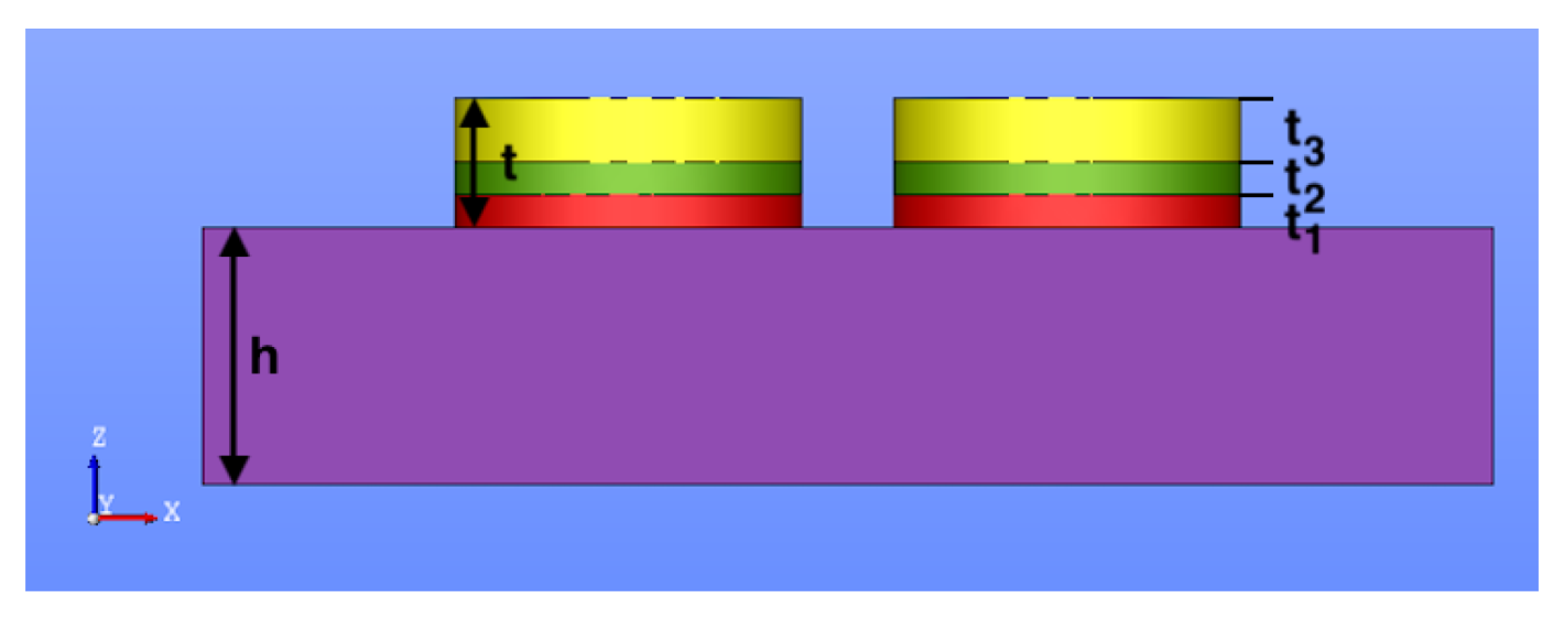
Figure 17.
Plasmonic nanoantenna of Figure 13 with the gold nanoparticles divided in three layers with heights nm, nm, and nm.
Figure 17.
Plasmonic nanoantenna of Figure 13 with the gold nanoparticles divided in three layers with heights nm, nm, and nm.


Table 1.
Patch antenna (Figure 9) eigenfrequencies with () and without (, ) feeding line (red contour) versus those in the absence of patch radiator and feeding line ().
Table 1.
Patch antenna (Figure 9) eigenfrequencies with () and without (, ) feeding line (red contour) versus those in the absence of patch radiator and feeding line ().
| No | [THz] | [THz] | [THz] | [THz] |
|---|---|---|---|---|
| 1 | 0.770 + j0.330 | 0.781 + j0.387 | 0.799 + j0.433 | 0.778 + j0.332 |
| 2 | 0.802 + j0.051 | 0.813 + j0.059 | 0.815 + j0.058 | 0.793 + j0.036 |
| 3 | 0.947 + j0.386 | 0.960 + j0.453 | 0.958 + j0.440 | 0.951 + j0.371 |
| 4 | 1.038 + j0.103 | 1.037 + j0.088 | - | 1.040 + j0.084 |
| 5 | 1.171 + j0.170 | 1.187 + j0.200 | - | 1.181 + j0.200 |
| 6 | - | - | - | 1.314 + j0.042 |
| 7 | 1.408 + j0.089 | 1.439 + j0.092 | 1.441 + j0.083 | 1.438 + j0.109 |
| 8 | 1.506 + j0.101 | 1.495 + j0.777 | 1.501 + j0.847 | 1.490 + j0.098 |
| 9 | 1.586 + j0.691 | 1.590 + j0.628 | 1.589 + j0.630 | 1.571 + j0.725 |
| 10 | 1.617 + j0.731 | 1.717 + j0.321 | - | 1.685 + j0.636 |
: Eigenfrequencies for the patch antenna of Figure 9 without the feeding line, based on the recursive formulation of Section 2.2.1; : Eigenfrequencies for the patch antenna of Figure 9 without the feeding line, based on the auxiliary field-based formulation of Section 2.2.2; : Eigenfrequencies for the finite grounded substrate of Figure 9 in the absence of the patch radiator and the feeding line, based on the auxiliary field-based formulation of Section 2.2.2; : Eigenfrequencies for the patch antenna of Figure 9, based on the auxiliary field-based formulation of Section 2.2.2.
Table 2.
Ten first eigenvalues and corresponding resonant wavelengths for the plasmonic nanoantenna (see Figure 13) using the auxiliary field-based formulation (Section 2.2.2). The last two columns refer to the eigenvalues and corresponding resonant wavelengths of the substrate (absence of gold particles). The eigenvalues appearing in bold () correspond to patch antenna modes.
| Plasmonic Nanoantenna | Substrate | |||
|---|---|---|---|---|
| No | ||||
| 1 | 9.451 + j4.102 | 664.8 | 9.425 + j4.061 | 666.7 |
| 2 | 9.488 + j3.693 | 662.2 | 9.437 + j3.950 | 665.8 |
| 3 | 9.506 + j3.899 | 661.3 | - | - |
| 4 | 9.938 + j4.197 | 632.2 | - | - |
| 5 | 12.210 + j3.273 | 514.6 | 12.166 + j3.545 | 516.5 |
| 6 | 12.226 + j3.403 | 513.9 | 12.193 + j3.395 | 515.3 |
| 7 | 12.290 + j3.649 | 511.2 | 12.202 + j3.369 | 514.9 |
| 8 | 12.321 + 3.656 | 510.0 | 12.264 + j3.672 | 512.3 |
| 9 | 12.395 + j3.310 | 506.9 | 12.419 + j3.452 | 505.9 |
| 10 | 12.455 + j3.428 | 504.5 | 12.445 + j3.498 | 504.9 |
Publisher’s Note: MDPI stays neutral with regard to jurisdictional claims in published maps and institutional affiliations. |
© 2021 by the authors. Licensee MDPI, Basel, Switzerland. This article is an open access article distributed under the terms and conditions of the Creative Commons Attribution (CC BY) license (https://creativecommons.org/licenses/by/4.0/).
Share and Cite
MDPI and ACS Style
Paschaloudis, K.D.; Zekios, C.L.; Trichopoulos, G.C.; Farmakis, F.; Kyriacou, G.A. An Eigenmode Study of Nanoantennas from Terahertz to Optical Frequencies. Electronics 2021, 10, 2782. https://doi.org/10.3390/electronics10222782
AMA Style
Paschaloudis KD, Zekios CL, Trichopoulos GC, Farmakis F, Kyriacou GA. An Eigenmode Study of Nanoantennas from Terahertz to Optical Frequencies. Electronics. 2021; 10(22):2782. https://doi.org/10.3390/electronics10222782
Chicago/Turabian StylePaschaloudis, Konstantinos D., Constantinos L. Zekios, Georgios C. Trichopoulos, Filippos Farmakis, and George A. Kyriacou. 2021. "An Eigenmode Study of Nanoantennas from Terahertz to Optical Frequencies" Electronics 10, no. 22: 2782. https://doi.org/10.3390/electronics10222782
Note that from the first issue of 2016, this journal uses article numbers instead of page numbers. See further details here.