Article

A Design Method of Compensation Circuit for High-Power Dynamic Capacitive Power Transfer System Considering Coupler Voltage Distribution for Railway Applications

CRRC Qingdao Sifang Rolling Stock Co., Ltd., Qingdao 266000, China
*
Author to whom correspondence should be addressed.
Electronics 2021, 10(2), 153; https://doi.org/10.3390/electronics10020153
Submission received: 4 December 2020 / Revised: 31 December 2020 / Accepted: 5 January 2021 / Published: 12 January 2021
(This article belongs to the Special Issue Wireless Power Transfer and Its Applications)

Abstract

:
Capacitive power transfer (CPT) is a promising method to solve the problems caused by the traditional Pantograph-catenary contact power supply for railway applications. In contrast, the CPT system suffers a broken risk because of the small coupling capacitor. This paper has analyzed the CPT coupler’s voltage distributions for dynamic CPT systems when high power is required in real railway applications. The triangle relationship among the coupler voltages is derived. The circuit of the CPT system to accolated the coupler voltage is analyzed. Then, the compensation parameters are given. With the adopted LCLC-CL topology, the design process is presented by considering the coupler voltages. An experimental setup is conducted to validate the proposed design method. The experimental results show that the system can achieve 3 kW output power with 92.46% DC-DC efficiency and the voltage distribution aggress well with the designed values.

1. Introduction

Traditionally, the railway power supply system mainly uses the pantograph-catenary (PC) method to power the moving locomotives [1,2]. The pantograph on the top of the locomotive uses sliding friction to get power from the already laid catenary. However, this kind of sliding flow has great hidden dangers: (1) Limits the increase of locomotive speed. The carbon brush on the pantograph obtains electricity by rubbing on the contact net. When the speed is further increased, the wear and tear of the carbon brushes become more serious, which accelerates the aging of the carbon brushes. Therefore, the locomotive speed must be limited within a specific range to ensure the normal working life of the carbon brushes. (2) Needs a large amount of system maintenance. The catenary is exposed to the air as a source of electrical energy. When there is extreme weather, such as strong wind, heavy rain, frost and snow, the receiving power grid and the catenary will not cooperate well, which will affect the regular power supply of the system. Therefore, it is necessary to propose a new power supply method to completely solve the problem of the traditional pantograph-net friction power supply and ensures the safe and reliable operation of rail transit power supply systems.
Wireless power transfer can deliver the electric power from the input source to the load with a contactless method, which has gained many researchers’ attention around the world [3,4,5,6,7]. Usually, the WPT system can be achieved by inductive or capacitive coupling for the high-power demanded system [8]. The former is called inductive power transfer (IPT) [9]. IPT system has been proposed and designed for railway applications. While the IPT system suffers from many Litz wire and magnetic cores to build a magnetic field, it will increase the system cost and weight. Additionally, the high magnetic field may introduce the eddy current loss in the nearby metal objects [10].
The latter is named capacitive power transfer (CPT) [11,12,13,14]. When the CPT system is used in the railway power supply system, the drawbacks introduced by the traditional PC supply system can be efficiently removed [15,16,17]. Further, the CPT system can be embedded under the ground, which can reduce system maintenance. The CPT system uses electric filed to achieve wireless power transfer that only required the think metal plates to form the coupler [18,19,20]. Therefore, the CPT system has advantages such as low weight and effective system cost. Different from the IPT, which uses the magnetic field as the transfer medium, the CPT system uses an electric field that does not induce the eddy current in the nearly metal things that are suitable for railway applications and the container power supply system [21,22,23].
However, the CPT system is suffering from a small coupling capacitor. When the transfer distance is up to several hundred mm, the mutual capacitor is usually only at the pF level. As shown in Reference [24], the mutual capacitor is 13.84 pF when the transfer distance is 150 mm with four 650 mm × 650 mm square metal plates for the CPT coupler. To achieve high power transfer, the CPT system mainly depends on two things: increasing the working frequency of the inverter and increasing the voltage of the coupling coupler [25,26,27,28,29]. At present, the working frequency of the inverter has been increased to several MHz. Considering the available working switching devices, it is a huge challenge to increase the transfer power by improving the switching frequency. The voltage of the coupling coupler has also been increased to several kV to achieve kW-level power transmission. As shown in Reference [10], the coupler voltage is up to 7.62 kV when the transfer power is only 2.4 kW.
Railway applications have the characteristic of the large transfer power. For example, the effective power of high-speed railways can reach 3–10 MW [4]. Applying the CPT system to the railway power supply will inevitably face the problem of excessive CPT system voltage. At the same time, the transfer distance of rail transit applications is relatively short, often at the several tens of mm level. The coupling coupler is vulnerable to breakdown. To solve the problem of excessively high voltage of the CPT system under high power, Reference [30] has proposed a voltage optimization strategy for the high power system that can reduce the maximum voltage for the compensation component. However, this method uses numerical analysis and calculation. Additionally, the voltage distribution of the CPT coupler has not been analyzed clearly. Therefore, this method is difficult to design the high power CPT system considering the coupler voltages. Reference [31] proposed a series of compensation topologies that can achieve maximum power transmission under rated voltage. However, only the voltage distribution of the compensation topology is considered. The analysis of the coupler voltage is insufficient. At the same time, this method is aimed at the CPT coupler for electric vehicles, which is different from the coupling mechanism of rail transit.
This paper proposes a compensation circuit design method for the High-power dynamic CPT system to charge the railway applications, considering the coupler volage distribution. With the proposed design method, the voltages of the CPT coupler can be allocated reasonably by considering the arcing coupler risks, which is important for the high power demanded railway applications. The coupler voltage is analyzed by considering the system transfer power. Then, the design steps of the compensation circuit are given. An example CPT system with an LCLC-CL circuit is presented with the proposed design method. Finally, an experimental system is constructed and verified with the designed system. Experimental results show that the built system can achieve 3 kW output power with 92.46% DC-DC efficiency, and the voltage phase of the coupler is nearly 60 degrees, which validates the effectiveness of the coupler voltage distribution.

2. System Configuration and Analysis

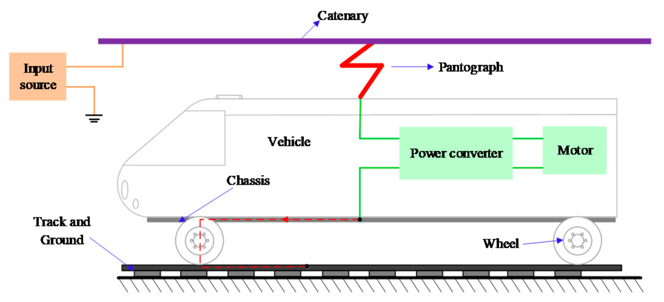
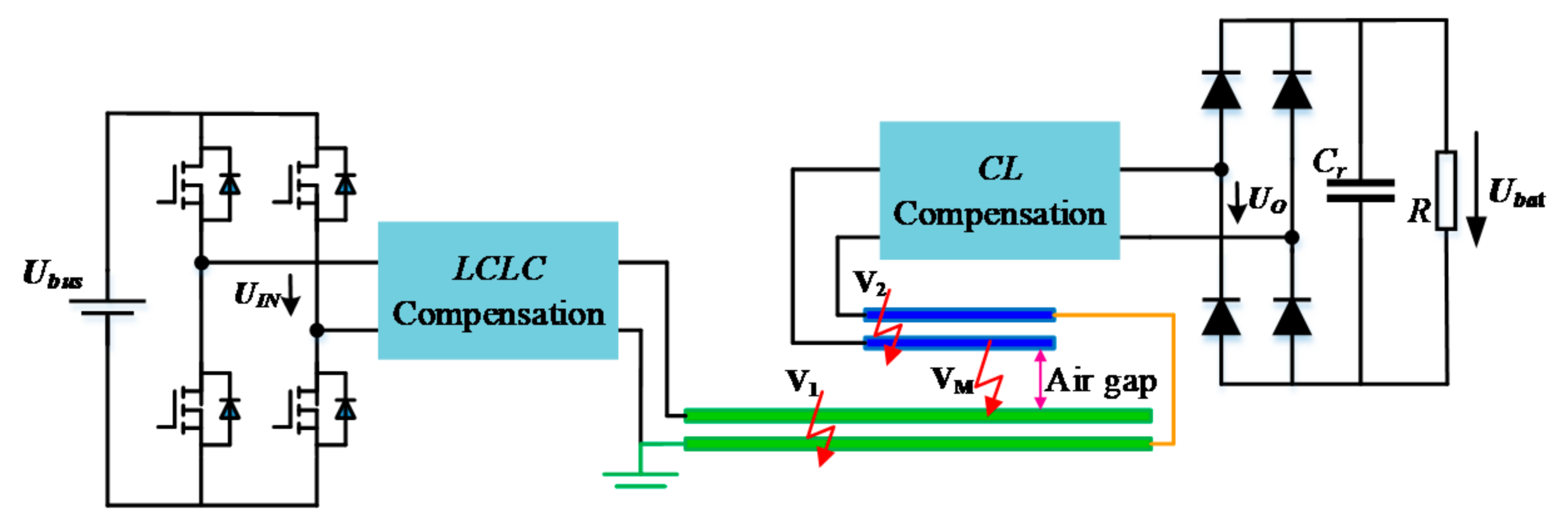
2.1. CPT Configuration for Raliway Applicaions

The traditional catenary pantograph power supply system is shown in Figure 1. The catenary is located on the top of the locomotive and connected with the locomotive by the pantograph. When the locomotive moves on the track, the sliding motion between the pantograph slide plate and the catenary occurs, and the electric energy is transferred from the catenary to the locomotive through the pantograph. In essence, the catenary and locomotive are directly connected. At present, the PC contact power supply system is the main power supply method for the electric locomotive. However, this system is vulnerable to environmental impact and a large number of maintenance deficiencies.
As a contactless power supply method, the CPT system can effectively solve the above problems. The CPT is applied to the railway power supply system, and the system structure is shown in Figure 2. Compared to the traditional PC power supply system, the CPT system does not need a catenary to be installed on the top of the locomotive. The transfer coupler can be placed on the bottom of the locomotive, which can simplify the complexity of the power supply system. At the same time, the coupler can be integrated into the track, which can reduce the maintenance of the power supply system. In extreme weather such as gale and blizzard, the CPT system can supply power for locomotive safely and effectively. Besides, the CPT system provides power to the locomotive in a non-contact way, which will not limit the running speed of the locomotive due to wear and other problems.
Generally, the CPT system requires four plates to form a CPT coupler and to construct a complete current loop. However, the car body is directly connected to the ground and the steel rail through the wheels in the railway power supply system; it can form a natural ground current channel. When the CPT system is used to the railway power supply system, only two plates are needed. As shown in Figure 2, P2 represents the transmitter plate, which is installed on the ground side. The receiver plate is installed at the end of the car body marked as P3. Since the transfer power of the railway power supply system is relatively high, an additional ground isolation layer can be added to the space between the car body and the receiving plate for system safety consideration as well as the ground and the transmitter plate to prevent high voltage from causing breakdown problems. The DC input at the transmitter is inverted into a high-frequency AC by an inverter, and power is supplied to the plates after the compensation topology. The high voltage of the transfer port generates a displacement current, which realizes the transfer from the transmitting end to the receiving end and the wireless power transfer of the electric energy. The receiver plate will get the ground electric energy to supply power for the locomotive load after the compensation topology and the rectifier.

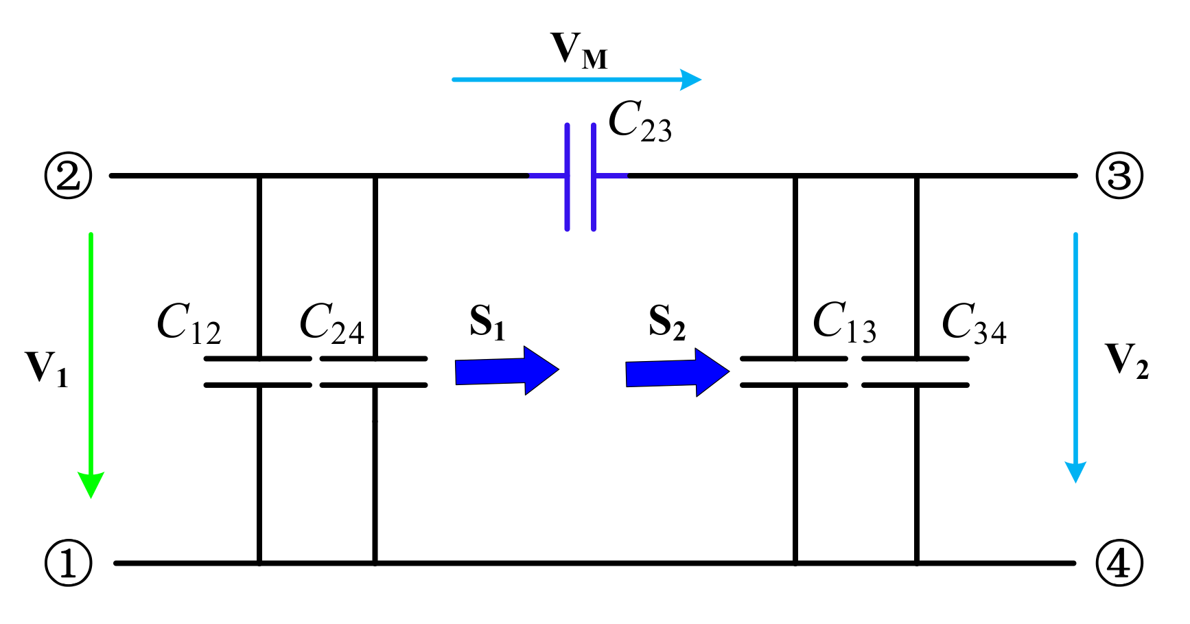
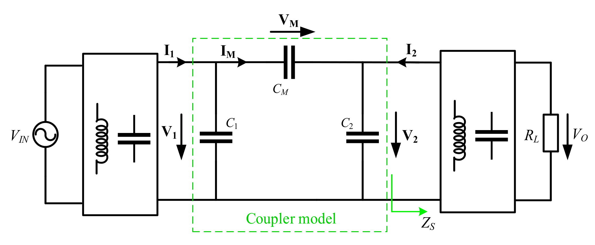
2.2. CPT Coupler Model

Since the receiver plate, the transmitter plate, the steel rail and the ground, the car body and the chassis will generate a coupling capacitor with each other; the equivalent coupling model of the CPT system is shown in Figure 3. Since the ground and the car body are connected naturally, there are a total of five coupling capacitors. Due to the mutual isolation between the plates, C12 >> C24, C34 >> C13. C23 is the critical capacitor to realize CPT transfer, and it can also be defined as mutual capacitance CM. Its value is directly related to the system transfer power.
The CPT coupler mainly has two port voltages V1, V2 and one transfer voltage VM. During the system design process, these three voltages must be analyzed to prevent system breakdown caused by excessive voltage during the high-power demand to ensure system safe and reliable operation.

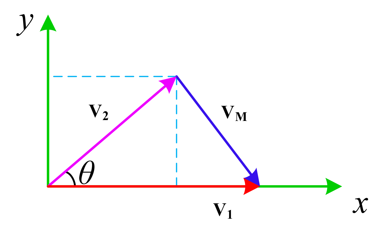
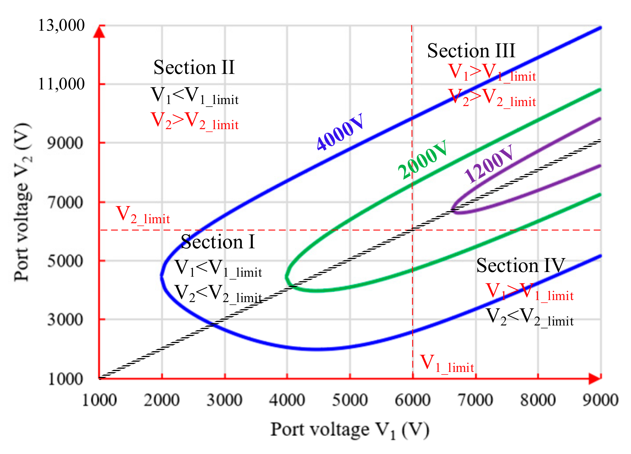
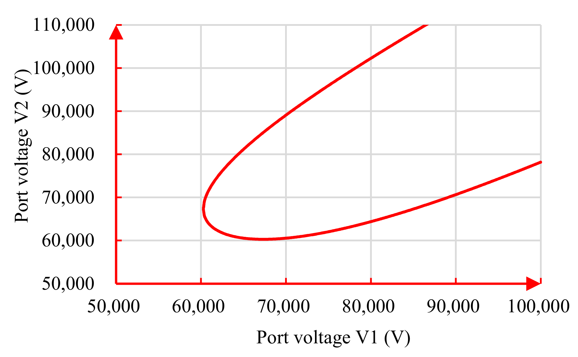
2.3. Analysis of System Transfer Power and Coupler Voltage

As shown in Figure 3, there are three voltages in the CPT coupler, and it is necessary to analyze the relationship between the coupler voltages and the system transfer power. The relationship between the three voltages is shown in Figure 4.
Since V1 = V2 + VM, the three coupler voltages has a triangular relationship, as shown in Figure 4. When analyzing the relationship between the coupler voltage and system transfer power, only two of them need to be considered. This paper selects the port voltages V1 = V2 for further analysis. As shown in Figure 4, V1 is selected as the reference voltage, and the phase difference between V2 and V1 is θ, which is determined by the amplitude of V1, V2 and VM. Define V1 and V2 as the voltage amplitudes of V1 and V2 respectively, then V2 can be expressed as
V 2 = V 2 ( cos ( θ ) + j sin ( θ ) )
The current IM flowing through the mutual capacitor CM can be derived as
I M = V 1 V 2 j ω C M = ω C M V 2 sin ( θ ) + j ω C M ( V 1 V 2 cos ( θ ) )
ω is the working angle frequency.
The input and output inspecting power of CM can be calculated as
S 1 = V 1 ( I M ) = ω C M V 1 V 2 sin ( θ ) j ω C M V 1 ( V 1 V 2 cos ( θ ) ) S 2 = V 2 ( I M ) = ω C M V 1 V 2 sin ( θ ) + j ω C M V 2 ( V 2 V 1 cos ( θ ) )
Since the CPT coupler is a reactive power transmission mechanism, the active power transmitted by the system can be expressed as:
P = Re ( S 1 ) = Re ( S 2 ) = ω C M V 1 V 2 sin ( θ )
Rewrite Equation (4), and we can get
P ω C M = V 1 V 2 sin ( θ ) = 2 S Δ
As shown in Equation (5), S is the area of the triangle formed by the voltages V1, V2 and VM. Therefore, for a particular coupling mechanism, the system transfer power is proportional to S. For a specific coupling mechanism and system transmission power, there are countless ways to configure the CPT coupler’s three voltages. The triangle relationship shows that there is no simultaneous minimum of those three voltages. Reducing one of the voltages must be at the expense of increasing the other voltages. Therefore, in the system design, the above triangle relationship can be used to configure the system compensation topological structure and reasonably distribute the coupler voltage to prevent the breakdown risk caused by high power demand.
An engineering tradeoff needs to be made to ensure that coupler voltage does not damage the device and prevent it from the coupler broken-down.
The Helen formula states that the area of a triangle whose sides have lengths a, b, and c is
A = s ( s a ) ( s b ) ( s c )
where s is the semi-perimeter of the triangle; that is,
s = a + b + c 2
According to the Helen formula in Equation (6), the voltage distribution relationship of the coupling coupler under the rated transfer power can be derived. Assuming that the working frequency of the CPT system is 1 MHz and the equivalent coupling capacitance is 20 pF, the voltage distribution of the coupling coupler can be represented in Figure 5. Figure 5 shows the variation trend of V1 and V2 under different voltage VM values. The black line represents the value line of V1 = V2. It is clear that the voltages under V1 = V2 gradually decrease as the VM voltage increases. When VM = 1200 V and V1 = V2, the value is 6631 V; when VM = 4000 V, the value of V1 = V2 is reduced to 2821 V. In the case of a particular triangle area, there is a case where a certain side length is the smallest, limited by the side length of the triangle. As shown in Figure 5, when VM = 2000 V, the minimum value of V2 is 3979 V, and the corresponding value of V1 is 4453 V. It is worth noting that, when the value of V2 is the smallest, the related voltage V1 is not the smallest at the same time. Therefore, when designing the system to optimize the voltage distribution, it is necessary to determine the voltage distribution of the coupling mechanism according to different withstand voltage requirements. Assuming that the maximum withstands voltages of V1 and V2 are both 6000 V, Figure 5 can be divided into four sections. The first section is to meet the voltage requirements, and the second, third and fourth sections all have voltages exceeding the rated limit. Therefore, when the voltage parameters are selected in the system design, only values V1 and V2 in the first section can be taken. As shown in Figure 5, when VM = 1200 V, all the calculated V1 and V2 that meet the conditions are not in the first section, so the system design requirements cannot be met, and a new voltage VM needs to be selected again. When VM is increased to 2000 V or 4000 V, the voltage configuration parameters in the first section can be set.

3. Compensation Topology Analysis

From the above analysis, it is known that the voltage distribution of the coupling coupler under safe conditions can be solved according to the rated transfer power, the coupling coupler and other working conditions of the system. Then, the system design can be completed according to the voltage distribution that meets the safety conditions and the appropriate compensation topology. Assuming that the voltages V1, V2 and VM of the coupling mechanism are determined, the phase difference θ of the voltages V1 and V2 can be calculated by the law of cosines and can be expressed as:
cos ( θ ) = V 1 2 + V 2 2 V M 2 2 V 1 V 2
Assume that the equivalent impedance after the coupling capacitor CM is ZS, as shown in Figure 6, ZS = A + jB. Then, the current IM flowing through CM can be expressed as
I M = V 2 Z S = V 2 A A 2 + B 2 j V 2 B A 2 + B 2
Further, port voltage V1 can be calculated as
V 1 = I M j ω C M + V 2
Therefore, the ratio of V2 and V1 can be derived as
V 2 V 1 = G V _ Re + j G V _ I m
GV_Re and GV_Im represent the real and imaginary parts of the voltage ratio, respectively, and can be expressed as
G V _ Re = ω C M B 1 ω 2 C M 2 A 2 + ω 2 C M 2 B 2 2 ω C M B + 1 + 1 G V _ I m = ω C M A ω 2 C M 2 A 2 + ω 2 C M 2 B 2 2 ω C M B + 1
Comparing Equations (1) and (10), the system should satisfy
U 2 U 1 cos ( θ ) = G V _ Re U 2 U 1 sin ( θ ) = G V _ Im
According to Equation (11), A and B can be solved.
A = U 1 U 2 sin ( θ ) ω C M U 1 2 2 ω C M U 1 U 2 cos ( θ ) + ω C M U 2 2 cos ( θ ) 2 + ω C M U 2 2 sin ( θ ) 2 B = U 2 2 cos ( θ ) 2 + U 2 2 sin ( θ ) 2 U 1 U 2 cos ( θ ) ω C M U 1 2 2 ω C M U 1 U 2 cos ( θ ) + ω C M U 2 2 cos ( θ ) 2 + ω C M U 2 2 sin ( θ ) 2
Therefore, Equation (13) is satisfied to ensure that the coupling coupler is within the safe voltage range when designing the parameters of the receiving end of the system. At the same time, Equation (12) shows that the topological parameters of the receiver side determine the phase relationship between the port voltages V1 and V2 under the condition of a particular coupling mechanism and working frequency. Then, the transfer voltage VM is determined.
For a high-power CPT system, the compensation topology of the transmitter and receiver side need to increase the coupling coupler port voltage to a higher power level. Therefore, the compensation parameters of the system transmitter and receiver side can be designed according to the input and output requirements of the system.

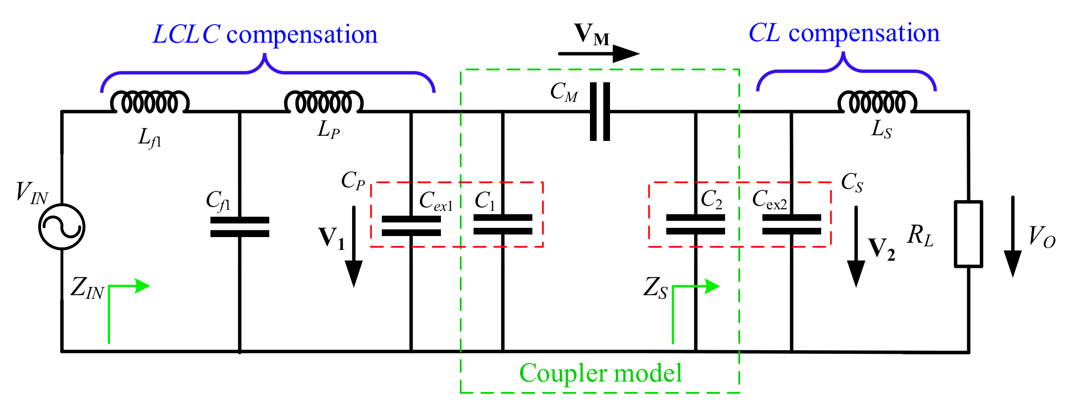
4. A Design Example System with an LCLC-CL Compensation Circuit

4.1. System Structure and Compensation

To ensure the coupler voltage distribution in a safe working situation, this paper gives detailed design steps based on the LCLC-CL compensation topology, as shown in Figure 7. The LCLC topology is applied to the transmitter, and the CL compensation topology is used on the receiver. The equivalent circuit is shown in Figure 8. The coupling coupler is replaced by the equivalent coupler model circuit, as shown in Figure 3.
Due to the filtering effect of the high-order compensation topology, the output power of the inverter is represented by a sinusoidal voltage source VIN to simplify the system analysis. RL is the equivalent load refracted to the front end of the rectifier bridge and satisfies [32]
R L = 8 π 2 R
Since Cex1 is connected in parallel with C1, CP can be used to represent the equivalent parallel capacitance, CP = Cex1 + C1. CS represents the parallel equivalent capacitance of Cex1 and C2, CS = Cex1 + C1.
The system compensation parameters meet the requirements
j ω L f 1 + 1 j ω C f 1 = 0 j ω L S + 1 j ω ( C S + C M C P C M + C P ) = 0 j ω L P + 1 j ω C f 1 + 1 j ω ( C P + C M C S C M + C S ) = 0

4.2. Compensation Parameter Design

When the CPT coupler and the appropriate voltage distribution of the coupling coupler are selected, the system compensation parameters on the transmitter and receiver side can be calculated separately. Since the phase relationship between the port voltages V1 and V2 is determined by the receiver topology of the mutual capacitor CM, the system parameters of the receiver side can be calculated first. Then, the compensation parameters of the transmitter side are calculated by the system output power.
As in Figure 8, the impedance ZS can be expressed as
Z S = 1 1 R L + j ω L S + j ω C S
Then, the imaginary and real parts of ZS can be calculated as
A = R L ω 4 C S 2 L S 2 + ω 2 C S 2 R L 2 ω 2 C S L S + 1 B = ω 3 C S L S 2 + ω C S R L 2 ω L S ω 4 C S 2 L S 2 + ω 2 C S 2 R L 2 ω 2 C S L S + 1
Submitting Equation (13) into Equation (17), compensation parameters LS and CS can be solved as
L S = R L 2 U 1 C M ( 2 U 2 sin ( θ ) ω U 1 R L C M + ω U 1 R L C M cos ( 2 θ ) ) ω R L 2 ω U 1 C M sin ( θ ) C S = 4 U 1 U 2 C M sin ( θ ) 2 ω U 1 2 R L C M 2 + 2 ω U 1 2 R L C M 2 cos ( 2 θ ) ) ω R L 2 U 2 C M + 2 U 1 C M cos ( θ ) 2 U 2
Further, the external parallel capacitor Cex2 can be derived as
C e x 2 = 4 U 1 U 2 C M sin ( θ ) 2 ω U 1 2 R L C M 2 + 2 ω U 1 2 R L C M 2 cos ( 2 θ ) ) ω R L 2 U 2 C M + 2 U 1 C M cos ( θ ) 2 U 2 C 2
For the calculation process of the compensation topology parameters on the transmitter, the following steps can be given. As shown in Figure 8, the system input impedance ZIN of the inverter can be expressed as
Z I N = j ω L f 1 + 1 1 1 1 Z S + 1 j ω C M + j ω L P + j ω C f 1
Submitting Equation (15) into Equation (20), ZIN can be simplified as
Z I N = R L C M 2 C f 1 2 ( ω 2 C S L S + ω 2 C M L S 1 ) 2
To simplify the system analysis, the system compensation device is assumed to be no power loss, then the system input and output satisfies
V I N 2 Z I N = V O 2 R L
Submitting Equation (21) into Equation (22), we get Cf1.
C f 1 = ω 2 L S ( C S + C M ) 1
Then, submitting Equations (18) and (23) into Equation (15), compensation parameters Lf1, LP and CP can be derived as
L f 1 = 1 ω 2 C f 1 C P = C M ω 3 C S C M L S ω 2 C S L S + ω 2 C M L S 1 L P = L S C f 1 C S 2 + 2 L S C f 1 C S C M + L S C f 1 C M 2 C f 1 C M 2 C f 1 C M C M 2 + C f 1 C S ω 2 C f 1 C M 2
The external parallel capacitor Cex1 can be calculated as
C e x 1 = C P C 1 = C M ω 3 C S C M L S ω 2 C S L S + ω 2 C M L S 1 C 1
As shown in Equations (15) and (25), when compensation parameters satisfy that
C 2 = C S C 1 = C M ω 3 C S C M L S ω 2 C S L S + ω 2 C M L S 1
We can find that Cex1 = Cex2 = 0. Then, the adopted LCLC-CL topology can be simplified to the LCL-L structure, which simplifies the system construction. In this paper, we use LCLC-CL compensation to increase the freedom of the system design.
Summarizing the above design steps, the specific system design process is as follows:
  • Determine the dimension of the CPT coupler and calculate the coupling capacitance CM, select the appropriate coupling coupler voltages V1, V2 and VM according to the analysis in Section 2, and calculate the phase difference between the voltages V1 and V2;
  • Calculate the compensation parameters of the receiver side with output voltage VO and the port voltage V2, and the phase difference of the port voltages V2 and V1;
  • Derive the compensation parameters of the transmitter side with the system input voltage VIN, port voltage V1.

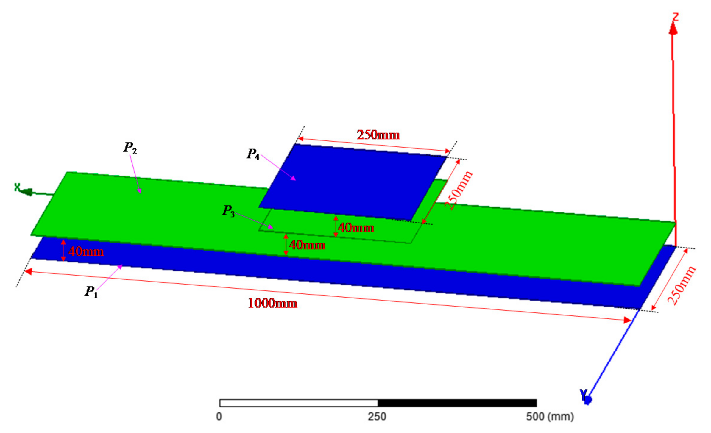
4.3. Coupler Dimension

Taking into account the available aluminum plate in our laboratory, this design selected two 1000 mm × 250 mm × 1 mm and two 250 mm × 250 mm × 1 mm aluminum plates to construct the CPT coupler. The 3D view of the coupler is shown in Figure 9. The distance between the transmitter and the receiver plate (the distance from P2 to P3) is 40 mm, and the distance from P1 to P2, and P3 to P4 are also set to 40 mm. The finite element analysis by the Maxwell 3D tool can be used to derive the coupling capacitor between every two plates, and the analysis results are presented in Table 1. According to the analysis results, CM = 19.66 pF, C1 = 84.45 pF, and C2 = 17.34 pF.
Since the distance between P1 and P2, P2 and P3, as well as P3 and P4 are same to 40 mm, and there is no additional insulation material between the sending and receiver side, the CPT coupler in V1, V2 and VM directions has the same voltage withstand level. Therefore, we defined that V1 = V2 = VM. Further, we can derive that the phase difference θ is 60°, and we can get
sin ( θ ) = 3 2 cos ( θ ) = 1 2

4.4. Compensation Parameter Calculation
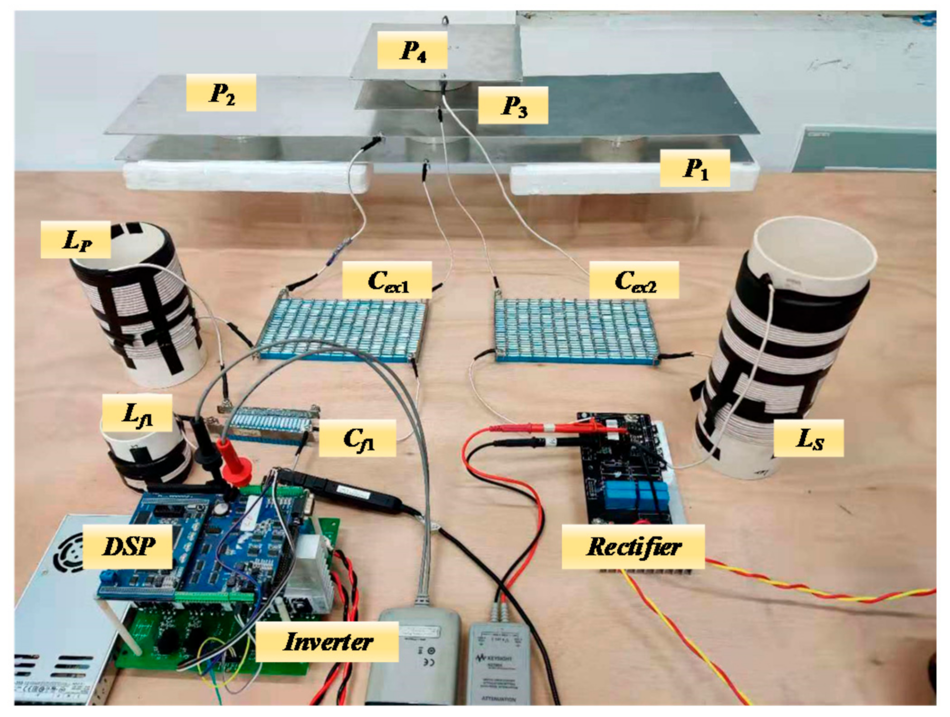
The system compensation parameters of the designed 3 kW scale down system is shown in Table 2. The CPT coupler has the parameters selected in the previous section. The working frequency is chosen as f = 500 kHz, and the equivalent mutual capacitor CM is 19.66 pF. Taking Equation (15) and V1 = V2 = VM into Equations (4) and (5), we can derive that:
V 1 = V 2 = V M = 7.49   kV

5. Experiment

5.1. Experiment Setup

To verify the effectiveness of the design method proposed in this paper, a 3 kW CPT experimental system was built, as shown in Figure 10. The structure and size of the CPT coupler are consistent with Figure 9. Two aluminum plates with 1000 mm × 250 mm are used to simulate the ground (P1) and the transmitter plate (P2), and two aluminum plates of 250 mm × 250 mm are used to model the receiver plate (P3) and vehicle (P4). The thickness of the above four aluminum plates is 1 mm. PVC tubes separate four aluminum plates, and the distance between adjacent aluminum plates is 40 mm. The operating frequency of the experimental system is 500 kHz. To reduce the Litz wire loss caused by the skin effect, the connecting wire and compensation inductor adopt 1500 strands Litz-wire with 50 μm diameter. The compensation capacitor in this experiment is composed of high-power and high-frequency thin-film capacitors made by KEMET. To improve the withstand voltage and current capability of the compensation capacitor, the compensation capacitor is formed of multiple sets of capacitors in a series. The wide bandgap devices Silicon carbide (SiC) MOSFETs C2M0080120D from CREE are used to make the inverter on the sending side, and SiC diodes from Global Power are adopted to construct the rectifier. The control single is produced by a digital DSP controller TMS, and is 28,335 for the high-frequency inverter. The load is modeled by Electronic load IT8816B.

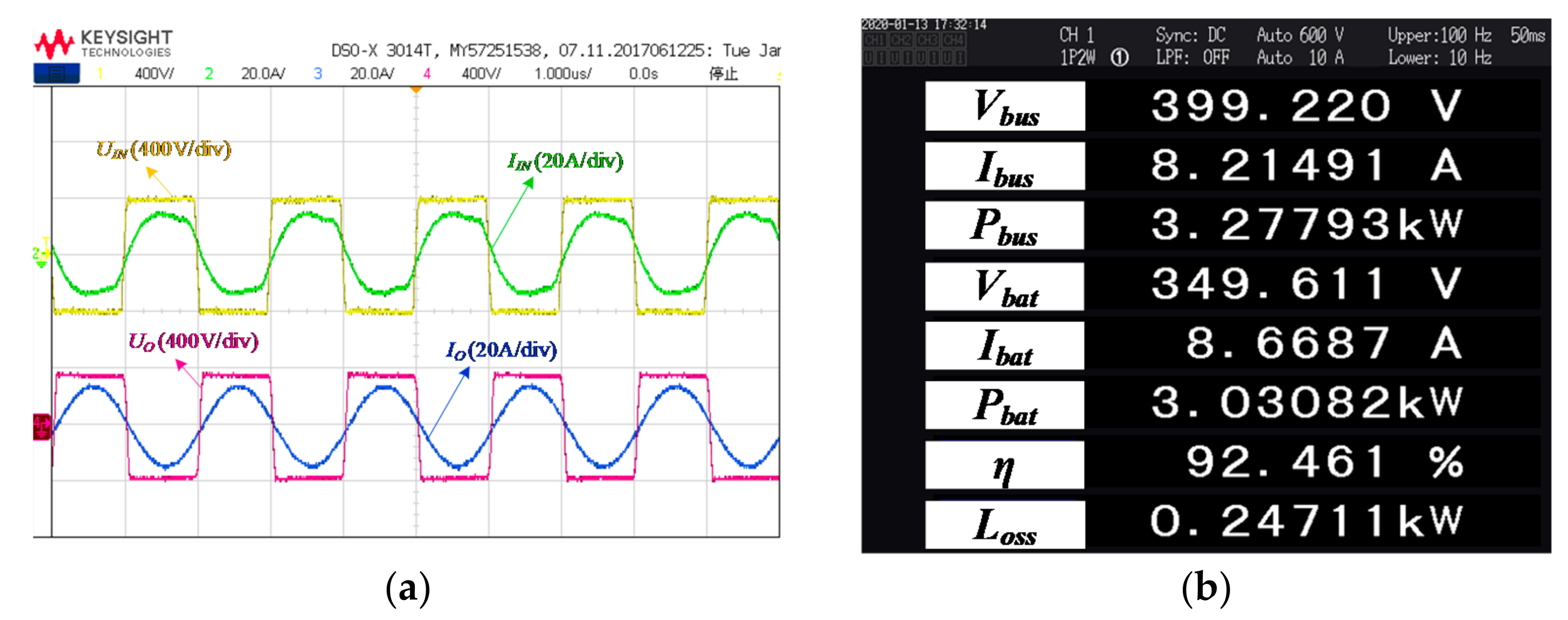
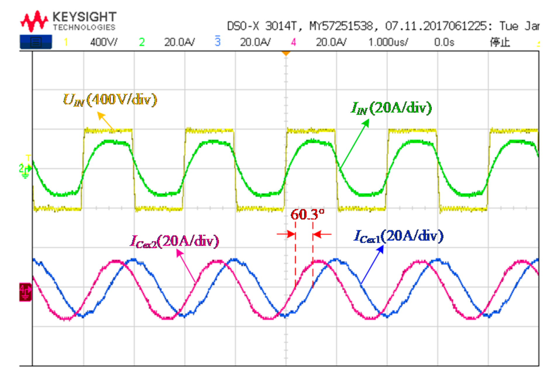
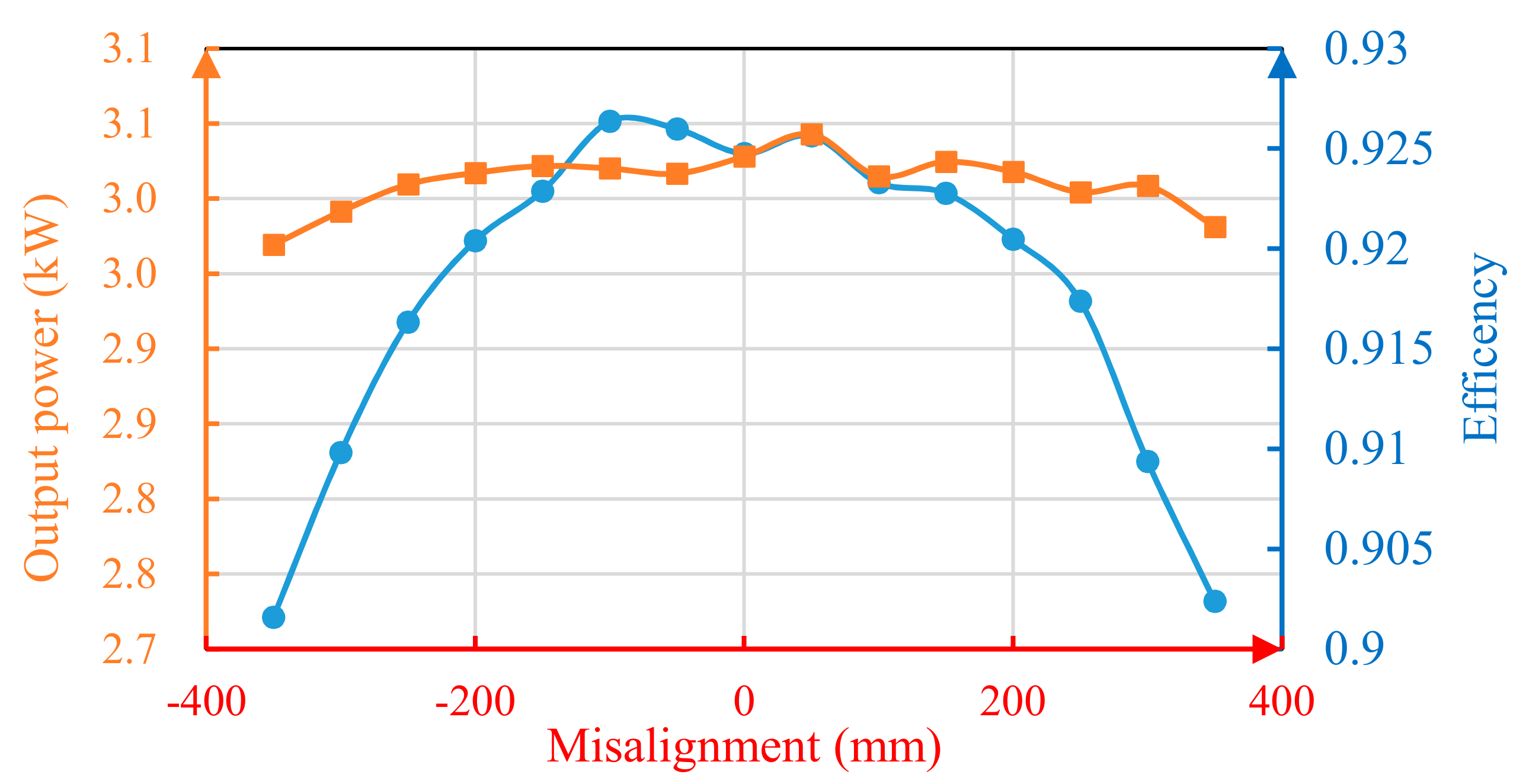
5.2. Experiment Results
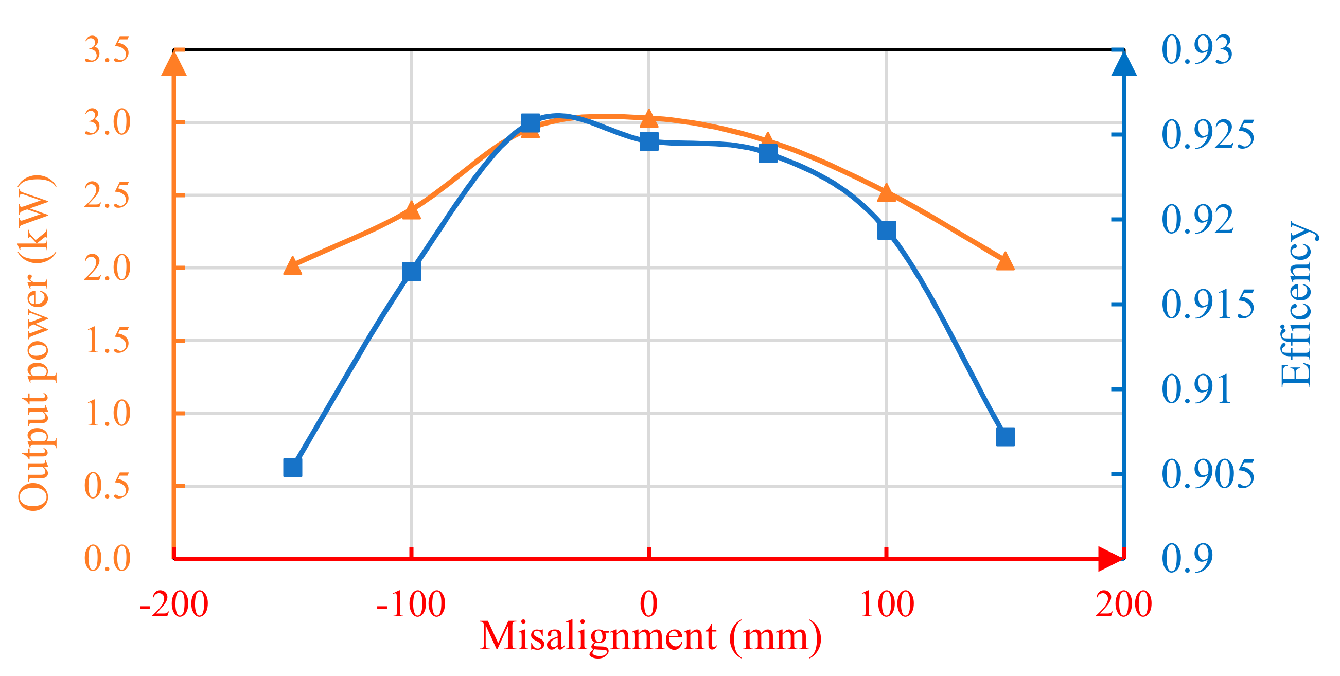
Figure 11a shows the experimental test results of the input and output waveforms. The output current and voltage of the inverter are nearly in phase. To improve inverter efficiency, the compensation inductor is built more extensively than the designed value. The inverter output impedance is slightly inductive, and the inverter can achieve zero voltage switch (ZVS). Figure 11b is the test result of the system DC-DC efficiency under the designed transfer power. When the system input voltage is 399.22 V, and the output reaches the deigned voltage of 349.61 V, the system transfer power is up to 3 kW with a DC-DC of 92.46%.
When the system operates at the maximum transfer power condition, the currents flowing through the compensation capacitors Cex1 and Cex2 are presented in Figure 12. The RMS values of ICex1 and ICex2 are 9.2 A and 8.8 A, respectively. The phase difference of the two currents is close to 60°. Therefore, we can derive that the port voltages of the CPT coupler are almost equal. Considering the voltage triangle relationship, the transfer voltage VM is also the same as the port voltages V1 and V2, and the voltage phase difference among those three voltages is 60 degrees separately. Therefore, the validity of the design method in this paper is verified. Through the practical system parameter design, the voltage distribution problem under high-power CPT system transfer can be solved, and the safety and reliability of the system can be improved.
When the coupler has a misalignment in the Y-axis, the measurement results in system output power and transfer efficiency are shown in Figure 13. With the increase of the coupler misalignment, the output power and efficiency of the system will decrease accordingly. When the maximum misalignment is 150 mm, the efficiency of the system is reduced from 92.46% to 90.57%, and the transfer power is reduced from 3 kW to 2 kW. The output power is reduced by 33%, which is mainly due to the large reduction of the mutual capacitor.
Figure 14 shows the power output power and efficiency test when the CPT receiver moves in the X-axis direction on the transmitter plate. The output power of the system varies from 2.7 kW to 3.0 kW when the receiver is moving. The maximum fluctuation of the output power is 9%. During the moving process, the DC-DC transmission efficiency of the system can be maintained above 92%.

6. Discussion

When the proposed system is applied to the practical railway power supply system, the voltage distribution under the maximum transfer power must be considered for the coupler safety consideration. The coupling capacitance of the CPT system applied to the railway power supply system is estimated to be as large as 4.4 nF [33]. Considering the 10 MW transfer power and the practical working frequency 200 kHz for the megawatts applications, the area of voltage triangle can be calculated based on Equation (5).
S Δ = P ω C M = 9.04 × 10 8
Considering the available space for the CPT system embedded in the railway system, the transfer distance dc is nearly 20–100 mm. When dc is selected as the minimum 20 mm, and the aching voltage Va for the air is 3 kV/mm [10]. Then, the transfer voltage VM can be calculated as
V M = d c V a k s = 20 × 3 × 0.5 = 30   kV
where ks is the safety coefficient for safety consideration and we set ks = 0.5 in this discussion.
Therefore, the relationship between V1 and V2 can be presented in Figure 15.
As shown in Figure 15, the minimum value of port voltage must be larger than 60.29 kV with the settled transfer distance to realize such a high-power CPT system in the railway power supply system. Therefore, the minimum distance between the receiving plate and the vehicle shell must be greater than 20 mm. High insulation materials can also be added into these gaps to improve the breakdown voltage and reduce the risk of system breakdown during high power transmission.

7. Conclusions

High voltage stressed on the CPT coupler is a critical problem that needs to be solved for the high-power CPT system adopted in the railway applications. In this paper, we have derived the relationship between the coupler voltages and the transfer power. We found that the tree coupler voltages in the railway applications can be presented as a triangle that is the property of the transfer power. When the coupling mutual capacitor and working frequency are specified, the triangle is determined with the settled transfer power. The tree coupler voltages can be accolated with the system requirements, while with the same triangle squares. The compensation parameters of the receiver side will determin the phase angle among three coupler voltages. A system design method is presented to accolade the coupler voltage considering the system coupler safety. With this method, an example of a 3 kW CPT system is designed and constructed. The experimental results show that the voltage distribution of the CPT coupler agrees well with the calculation results. The proposed design method is important for high power and short transfer distance, such as railway applicants.

Author Contributions

Conceptualization, J.L. and D.W.; Formal analysis, D.W. and J.Y.; Funding acquisition, J.L.; Methodology, J.Y.; Project administration, J.L.; Supervision, D.W., J.Y. All authors have read and agreed to the published version of the manuscript.

Funding

This work was supported by the National Key Research and Development Program of China under Grant 2016YFB1200602.

Data Availability Statement

No new data were created or analyzed in this study. Data sharing is not applicable to this article.

Conflicts of Interest

The authors declare no conflict of interest.

References

  1. Tan, P.-C.; Loh, P.C.; Holmes, D.G. Optimal impedance termination of 25-kV electrified railway systems for improved power quality. IEEE Trans. Power Deliv. 2005, 20, 1703–1710. [Google Scholar] [CrossRef]
  2. Tan, P.-C.; Morrison, R.E.; Holmes, D.G. Voltage form factor control and reactive power compensation in a 25-kV electrified railway system using a shunt active filter based on voltage detection. IEEE Trans. Ind. Appl. 2003, 39, 575–581. [Google Scholar]
  3. Li, Y.; Liu, S.; Zhu, X.; Hu, J.; Zhang, M.; Mai, R.; He, Z. Extension of ZVS region of series-series WPT systems by an auxiliary variable inductor for improving efficiency. IEEE Trans. Power Electron. 2020. [Google Scholar] [CrossRef]
  4. Kim, J.H.; Lee, B.-S.; Lee, J.-H.; Lee, S.-H.; Park, C.-B.; Jung, S.-M.; Lee, S.-G.; Yi, K.-P.; Baek, J. Development of 1-MW Inductive power transfer system for a high-speed train. IEEE Trans. Ind. Electron. 2015, 62, 6242–6250. [Google Scholar] [CrossRef]
  5. Hui, S.Y.R.; Zhong, W.; Lee, C.K. A critical review of recent progress in Mid-range wireless power transfer. IEEE Trans. Power Electron. 2014, 29, 4500–4511. [Google Scholar] [CrossRef] [Green Version]
  6. Mayordomo, I.; Drager, T.; Spies, P.; Bernhard, J.; Pflaum, A. An overview of technical challenges and advances of inductive wireless power transmission. Proc. IEEE 2013, 101, 1302–1311. [Google Scholar] [CrossRef]
  7. Kurs, A.; Karalis, A.; Moffatt, R.; Joannopoulos, J.D.; Fisher, P.; Soljacic, M. Wireless power transfer via strongly coupled magnetic resonances. Science 2007, 317, 83–86. [Google Scholar] [CrossRef] [Green Version]
  8. Dai, J.; Ludois, D.C. A survey of wireless power transfer and a critical comparison of inductive and capacitive coupling for small gap applications. IEEE Trans. Power Electron. 2015, 30, 6017–6029. [Google Scholar] [CrossRef]
  9. Li, Y.; Hu, J.; Lin, T.; Li, X.; Chen, F.; He, Z.; Mai, R. A new coil structure and its optimization design with constant output voltage and constant output current for electric vehicle dynamic wireless charging. IEEE Trans. Ind. Inf. 2019, 15, 5244–5256. [Google Scholar] [CrossRef]
  10. Lu, F.; Zhang, H.; Hofmann, H.; Mi, C. A double-sided LCLC-compensated capacitive power transfer system for electric vehicle charging. IEEE Trans. Power Electron. 2015, 30, 6011–6014. [Google Scholar] [CrossRef]
  11. Theodoridis, M.P. Effective capacitive power transfer. IEEE Trans. Power Electron. 2012, 27, 4906–4913. [Google Scholar] [CrossRef]
  12. Abramov, E.; Zeltser, I.; Peretz, M.M. A Network-based approach for modeling resonant capacitive wireless power transfer systems. CPSS Trans. Power Electron. Appl. 2019, 4, 19–29. [Google Scholar] [CrossRef]
  13. Luo, B.; Long, T.; Guo, L.; Dai, R.; Mai, R.; He, Z. Analysis and design of inductive and capacitive hybrid wireless power transfer system for railway application. IEEE Trans. Ind. Appl. 2020, 56, 3034–3042. [Google Scholar] [CrossRef]
  14. Luo, B.; Zhou, X.; Long, T.; Mai, R.; He, Z. Misalignment tolerance wireless power transfer system combining inductive and capacitive coupling. IET Electr. Power Appl. 2020, 14, 1925–1932. [Google Scholar] [CrossRef]
  15. Minnaert, B.; Costanzo, A.; Monti, G.; Mongiardo, M. Capacitive wireless power transfer with multiple transmitters: Efficiency optimization. Energies 2020, 13, 3482. [Google Scholar] [CrossRef]
  16. Ludowicz, W.; Pietrowski, W.; Wojciechowski, R.M. Analysis of an operating state of the innovative capacitive power transmission system with sliding receiver supplied by the Class-E inverter. Electronics 2020, 9, 841. [Google Scholar] [CrossRef]
  17. Sinha, S.; Kumar, A.; Regensburger, B.; Afridi, K.K. A new design approach to mitigating the effect of parasitic in capacitive wireless power transfer systems for electric vehicle charging. IEEE Trans. Transp. Electrif. 2019, 5, 1040–1059. [Google Scholar] [CrossRef]
  18. Muharam, A.; Ahmad, S.; Hattori, R. Scaling-factor and design guidelines for shielded-capacitive power transfer. Energies 2020, 13, 4240. [Google Scholar] [CrossRef]
  19. Abramov, E.; Alonso, J.M.; Peretz, M.M. Analysis and behavioural modelling of matching networks for resonant-operating capacitive wireless power transfer. IET Power Electron. 2019, 12, 2615–2625. [Google Scholar]
  20. Zou, L.J.; Zhu, Q.; Neste, C.W.V.; Hu, A.P. Modelling single-wire capacitive power transfer system with strong coupling to ground. IEEE J. Emerg. Sel. Top. Power Electron. 2019. [Google Scholar] [CrossRef]
  21. Park, C.; Park, J.; Shin, Y.; Kim, J.; Huh, S.; Kim, D.; Park, S.; Ahn, S. Separated circular capacitive coupler for reducing cross-coupling capacitance in drone wireless power transfer system. IEEE Trans. Microw. Theory Tech. 2020, 68, 3978–3985. [Google Scholar] [CrossRef]
  22. Luo, B.; Long, T.; Mai, R.; Dai, R.; He, Z.; Li, W. Analysis and design of hybrid inductive and capacitive wireless power transfer for high-power applications. IET Power Electron. 2018, 11, 2263–2270. [Google Scholar] [CrossRef]
  23. Vincent, D.; Huynh, P.S.; Azeez, N.A.; Patnaik, L.; Williamson, S.S. Evolution of hybrid inductive and capacitive AC links for wireless EV charging—A comparative overview. IEEE Trans. Transp. Electrif. 2019, 5, 1060–1077. [Google Scholar] [CrossRef]
  24. Luo, B.; Mai, R.; Guo, L.; Wu, D.; He, Z. LC–CLC compensation topology for capacitive power transfer system to improve misalignment performance. IET Power Electron. 2019, 12, 2626–2633. [Google Scholar] [CrossRef]
  25. Zhang, H.; Lu, F.; Hofmann, H.; Liu, W.; Mi, C.C. Six-plate capacitive coupler to reduce electric field emission in large air-gap capacitive power transfer. IEEE Trans. Power Electron. 2018, 33, 665–675. [Google Scholar] [CrossRef]
  26. Narayanamoorthi, R. Modeling of capacitive resonant wireless power and data transfer to deep biomedical implants. IEEE Trans. Components, Packag. Manuf. Technol. 2019, 9, 1253–1263. [Google Scholar] [CrossRef]
  27. Zhou, W.; Su, Y.G.; Huang, L.; Qing, X.D.; Hu, A.P. Wireless power transfer across a metal barrier by combined capacitive and inductive coupling. IEEE Trans. Ind. Electron. 2019, 66, 4031–4041. [Google Scholar] [CrossRef]
  28. Tamura, M.; Naka, Y.; Murai, K.; Nakata, T. Design of a capacitive wireless power transfer system for operation in fresh water. IEEE Trans. Microw. Theory Tech. 2018, 66, 5873–5884. [Google Scholar] [CrossRef]
  29. Zhaksylyk, Y.; Halvorsen, E.; Hanke, U.; Azadmehr, M. Analysis of fundamental differences between capacitive and inductive impedance matching for inductive wireless power transfer. Electronics 2020, 9, 476. [Google Scholar] [CrossRef] [Green Version]
  30. Mai, R.; Luo, B.; Chen, Y.; He, Z. Double-sided CL compensation topology based component voltage stress optimization method for capacitive power transfer charging system. IET Power Electron. 2018, 11, 1153–1160. [Google Scholar] [CrossRef]
  31. Luo, B.; Hu, A.P.; Munir, H.; Zhu, Q.; Mai, R.; He, Z. Compensation network design of CPT systems for achieving maximum power transfer under coupling voltage constraints. IEEE J. Emerg. Sel. Top. Power Electron. 2020. [Google Scholar] [CrossRef]
  32. Li, Y.; Hu, J.; Li, X.; Chen, F.; Xu, Q.; Mai, R.; He, Z. Analysis, design, and experimental verification of a mixed high-order compensations-based WPT system with constant current outputs for driving multistring LEDs. IEEE Trans. Ind. Electron. 2020, 67, 203–213. [Google Scholar] [CrossRef]
  33. Li, S.; Liu, Z.; Zhao, H.; Zhu, L.; Shuai, C.; Chen, Z. Wireless power transfer by electric field resonance and its application in dynamic charging. IEEE Trans. Ind. Electron. 2016, 63, 6602–6612. [Google Scholar] [CrossRef]
Figure 1. Pantograph-Catenary System for railway power supply.
Electronics 10 00153 g001
Figure 2. Configurations of the capacitive power transfer (CPT) system for railway applications.
Electronics 10 00153 g002
Figure 3. Full capacitor model of the CPT coupler.
Electronics 10 00153 g003
Figure 4. Relationships among three coupler voltages in the CPT coupler.
Electronics 10 00153 g004
Figure 5. Voltage distribution under different VM values when f = 1 MHz and CM = 20 pF.
Electronics 10 00153 g005
Figure 6. Equivalent circuit of the CPT system.
Electronics 10 00153 g006
Figure 7. Structure of the CPT system for railway applications.
Electronics 10 00153 g007
Figure 8. Simplified circuit topology with LCLC-CL compensation.
Electronics 10 00153 g008
Figure 9. 3D view of the specified CPT coupler.
Electronics 10 00153 g009
Figure 10. Experiment setup.
Electronics 10 00153 g010
Figure 11. Experiment test under the designed transfer power. (a) experimental test results of the input and output waveforms; (b) test results of the system DC-DC efficiency under the designed transfer power.
Electronics 10 00153 g011
Figure 12. Current waveforms of the capacitor Cex1 and Cex2.
Electronics 10 00153 g012
Figure 13. Output power and efficiency against the misalignment in the Y-axis direction.
Electronics 10 00153 g013
Figure 14. Output power and efficiency against the movement in the X-axis direction.
Electronics 10 00153 g014
Figure 15. Relationship between V1 and V2 when VM = 30 kV in the railway applications.
Electronics 10 00153 g015
Table 1. Maxwell analysis results of the capacitive coupler.
Simulation values (pF)C12 = 78.25C13 = 13.82C14 = 0
C23 = 19.66C24 = 6.21C34 = 18.19
Equivalent values (pF)CM = 19.66C1 = 84.45C2 = 17.34
Table 2. Main system parameters.
ParameterDesign ValueParameterDesign Value
f500 kHzP3000 W
Vbus400 VVbat450 V
CM19.66 pFRL67.5 Ω
Publisher’s Note: MDPI stays neutral with regard to jurisdictional claims in published maps and institutional affiliations.

