1. Introduction
The search and design of different kinds of sensors converting mechanical energy into electrical power has stimulated intensive studies of piezoelectric materials [
1]. Among such kinds of materials, it is necessary to point out very promising ceramics, like PbZrTiO
2 [
2], binary semiconductors (ZnO, GaN, InN) [
3], both in the bulk, as well as nanowires and nanobelts [
4].
Another direction of such research is based on laser operation by piezoelectricity [
5]. This effect was observed firstly in crystalline borate crystals [
6,
7,
8]. All of these treatments were performed in the near infrared with wavelengths as a rule up to 3 μm. Therefore, the main origin of the effect is caused by laser polarization of the crystalline electronic clouds. The phonon subsystem plays a secondary role here due to photoinduced phonons [
9]. However, for the chalcogenides, there exists huge electron-phonon anharmonicities [
10]. Therefore, one can expect that the excitations by mid-infrared light, like CO
2 lasers emitting at about 10.6 μm, may cause direct excitation of the phonon anharmonic resonances described by the third rank tensors.
As a consequence, in the present work, we will explore the possibility to operate by the piezoelectric coefficients using the excitations of the CO
2 lasers using two coherent beams incident at different angles, which may favor the occurrence of some anisotropic gratings. The previous experiments performed for other chalcogenides have shown the high stability and efficiency of such a grating [
11]. Following the general phenomenology, one can expect an occurrence of medium polarization possessing some charge density non-centrosymmetry. In the present work, we will compare the photoinduced effect caused by other lasers, like Nd:YAG (1064 nm), Er:glass (1540 nm), CO lasers (5.5 μm). Additionally, we will study the space distribution of the gratings for different geometries, energy powers and carrier photoconductivity kinetics.
2. Crystal Growth and Crystallochemistry
The titled crystals were grown by a method briefly described below. The quaternary sulfide Ag
2Ga
2SiS
6 was synthesized from high-purity raw materials: Ag (99.99 wt%), Ga (99.9997 wt%), Si (99.9999 wt%) and S (99.9999 wt%). The latter was obtained by the original technique described in [
12]. Silicon was crushed into fine powder in an agate mortar to increase its effective surface and consequently ease its interaction with the chalcogen. Calculated amounts of elements were placed in a quartz ampoule that was then evacuated and soldered. As the melt is aggressive to the container material, the ampoule was previously graphitized by acetone pyrolysis. The prepared ampoule was placed into a shaft-type furnace and heated at the rate of 30 K/h up to 720 K. The batch was kept at this temperature for 48 hours with the objective to complete the bonding of elementary sulfur. Further heating was at the rate of 20 K/h to 1270 K, with two intermediate stops at 970 K and 1170 K for 12 and 6 h, respectively. Upon reaching the maximum temperature, the quaternary compound is in the molten state according to the AgGaS
2-SiS
2 phase diagram [
13]. The furnace was kept at this temperature for 6 h and then cooled at the rate of 10 K/h to 670 K. After homogenizing annealing for 500 h, the synthesis process ended by quenching into cold water. The obtained alloy was a compact ingot of yellow color. The data of its examination by the XRPD method (DRON 4-13 diffractometer, CuK
α-radiation) agree well with our earlier results.
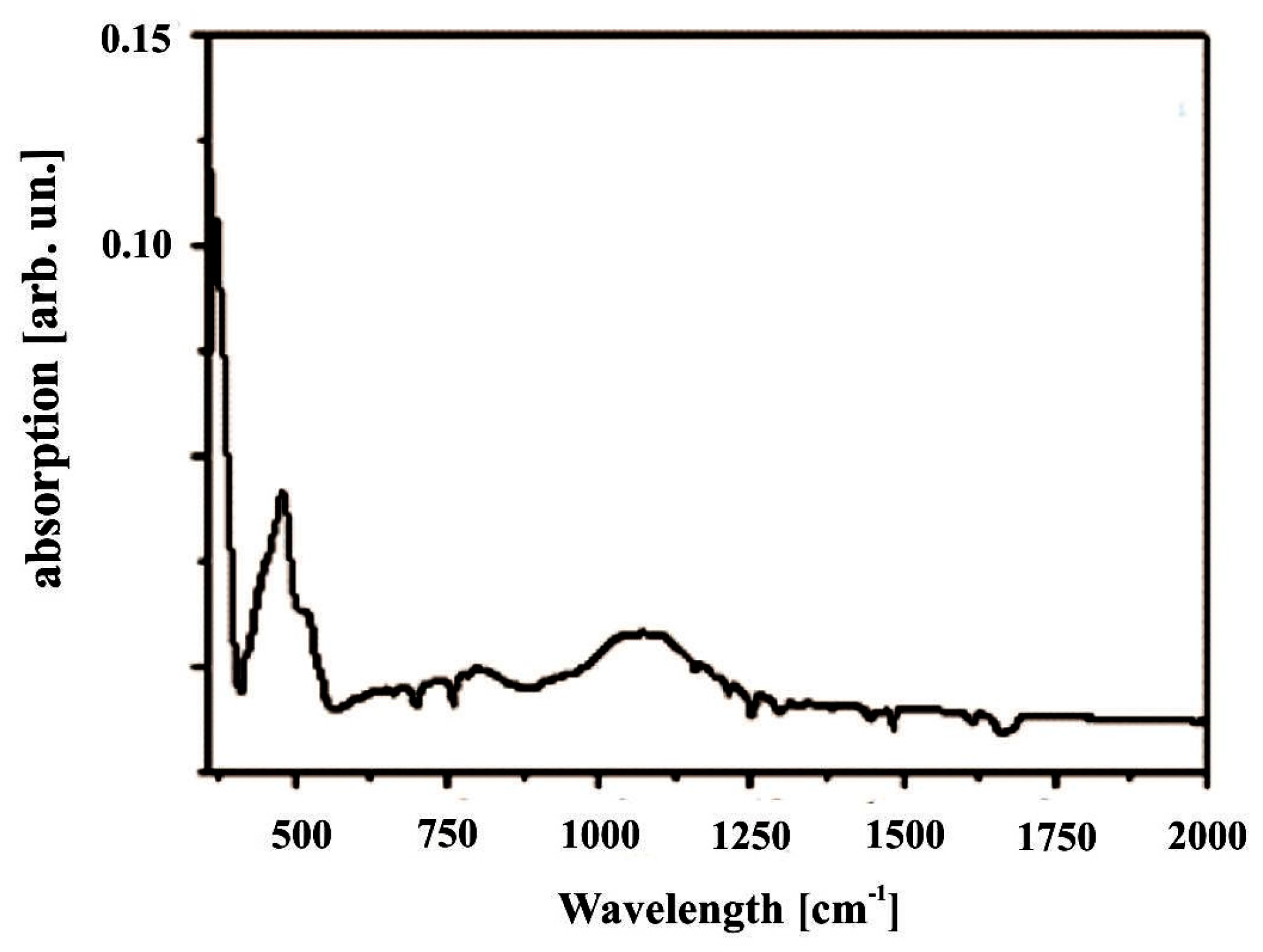
Following the presented data (see
Figure 1), one can conclude that only the CO
2 laser with a wavelength of 10.6 μm (about 943 cm
−1) and less CO (1886 cm
−1) may be close to the resonance IR frequencies and may effectively excite the phonon subsystem. The two other lasers are Er:glass 1540 nm (6490 cm
−1) and 1064 nm (9398 cm
−1), which are outside the phonon resonances. Therefore, for them, electron photopolarization will be dominating.
To understand the role of particular clusters in the observed effects and the possible origin of the defect states, we have done additional crystallochemistry and quantum chemical analysis.
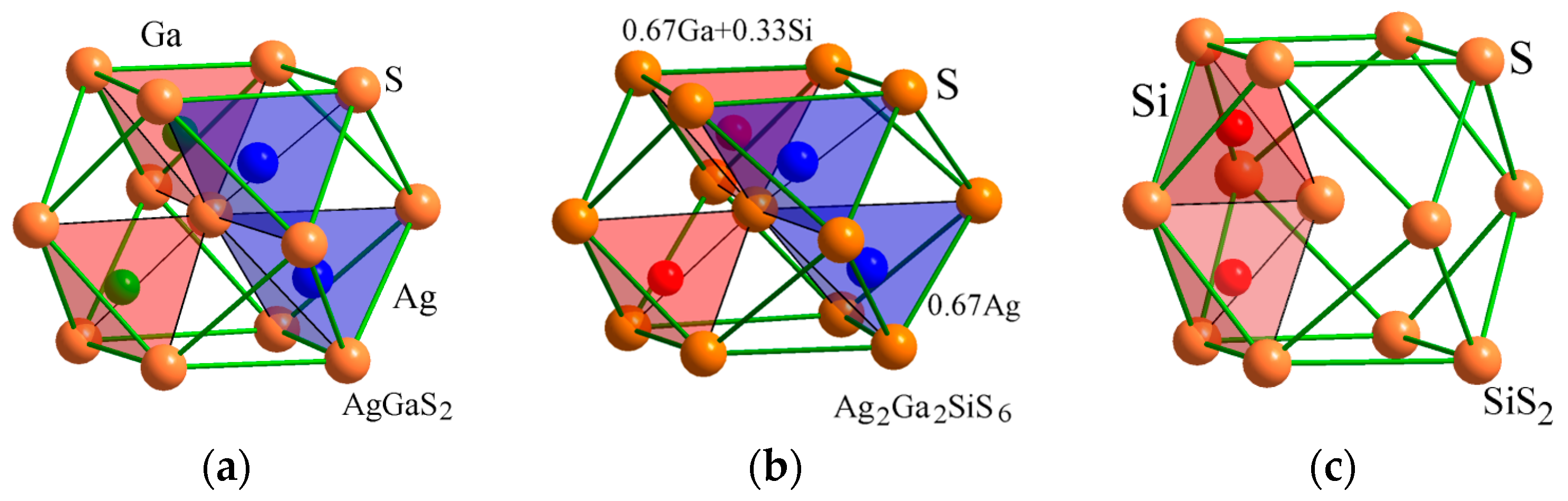
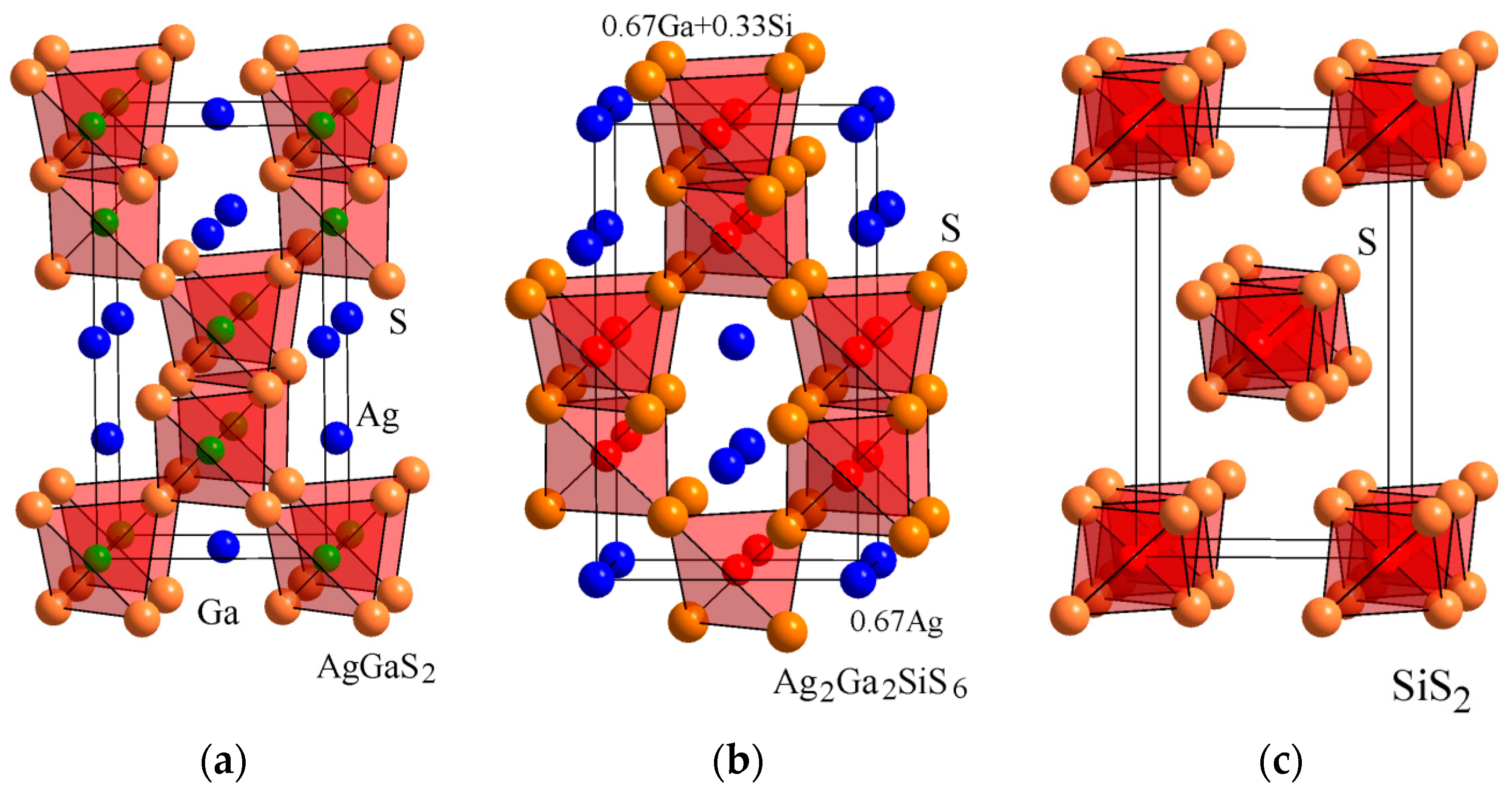
Their principal crystallochemistry architecture is presented in
Figure 2. Following the second coordination of sulfur [
14], the compounds AgGaS
2 [
15], Ag
2Ga
2SiS
6 [
13] and SiS
2 [
16] possess similar anionic sub-lattices in the form of cubooctahedra. Within the mentioned anionic sub-lattice, the cationic atoms occupy the equivalence tetrahedral voids. At the same time, the crystallochemistry of the crystals AgGaS
2, Ag
2Ga
2SiS
6 and SiS
2 may be presented (see
Figure 3) as formed by S tetrahedra. The Ag is situated in the channels between the tetrahedra for the case of AgGaS
2 and Ag
2Ga
2SiS
6 or even SiS
2.
As a consequence, the crystallochemistry of Ag2Ga2SiS6 may be presented as the isovalent simultaneous substitution of atoms Ag+ and Ga3+ by Si4+ for the structure AgGaS2 using a general schema: 3AgGaS2 − (Ag+ + Ga3+) + Si4+ = Ag2Ga2SiS6 (І). At the same time, the crystallochemistry of Ag2Ga2SiS6 may be presented as the iso-valent substitution of one Si4+ atom by atoms Ag+ and Ga3+ for the structure SiS2 in the following scheme: 3SiS2 − Si4+ + 2(Ag+ + Ga3+) = Ag2Ga2SiS6 (ІІ). During such a substitution, there occurs a transfer of the charge from channels between tetrahedra XSe44− into the middle of the tetrahedral in Case (ІІ) or, otherwise, from tetrahedral to inter-tetrahedral space (ІІ). During this charge transfer, there appears a change of ground state dipole moments, which is principal for the effects described by third rank tensors.
The considered crystallochemistry allows one to predict an opportunity to operate by the initial charge density distribution of the titled compounds. The two principal mechanisms for the formation of anisotropy in chalcogenides were described in [
9]. The first one deals with the excitations and photopolarization of the electronic charge density, and the second one deals with the multi-phonon excitations. The latter will be more effective for the wavelengths near 10.6 μm of the CO
2 laser.
To evaluate the importance of different structural fragment contributions, we have done additional quantum chemical calculations using the B3LYP DFT quantum chemical method as described in [
8]. It was concluded that Ga-S and Si-S clusters possess maximal ground state dipole moments equal to 8.7 D and 8.2 D, respectively. Moreover, using the same method, it was evaluated that the more probable are cationic defects, first of all Ga, Ag and less Si. The probability of their occurrence is 23%, 18% and 12%, respectively. At the same time, the probability of the anionic vacancies was almost an order less −4%.
In the present work, we will try to find a possibility to form an enhancement of the piezoelectric coefficients described by third rank polar tensors. We will perform the studies of the photoinduced piezoelectricity by IR laser of different wavelengths: Nd:YAG (1064 nm); Er:glass (1540 nm); CO (5.5 μm); and CO2 at 10.6 μm.
It is well known that the chalcogenide crystals are very sensitive to the external laser infrared light, and particular interest causes the coherent light treatment to be performed simultaneously by fundamental and doubled frequency coherent beam formed by second harmonic generation (SHG) beams. Such treatment causes an occurrence of some anisotropy even in the glasses, which is closely related to the third-order optical effects forming a medium anisotropy [
17,
18]. For this reason, two coherent pulse beams forming a grating in some wide range are used. Usually, this grating is non-centrosymmetry and may cause additionally laser-stimulated effects, like second harmonic generation, electrooptics and piezoelectricity [
19]. The use of light is a powerful tool for continuous changes of the charge density acentricity, defining the macroscopical third-order optical susceptibilities [
20].
3. Laser-Induced Piezoelectricity
Generally, the photoinduced piezoelectricity was measured by a method similar to that described in [
5] using a two-channel scheme, with the fundamental and doubled frequency beams, which are incident at different angles.
The space control of the piezoelectricity was done using a tip electrode moving through the studied samples. During illumination by the nanosecond pulsed lasers (CO2, CO, Nd:YAG and Er:glass), the optimal incident angles were varied within 18–26° with respect to the sample’s surfaces. The process of bicolor treatment had a duration of up to 2–3 min, and the measurements were performed for the fundamental probing beam during 10 s. The continuous wave (cw) one-mode polarized He-Ne lasers were used for the control of the occurred grating diffraction. The metrological statistics was done in more than 20 points of the surfaces.
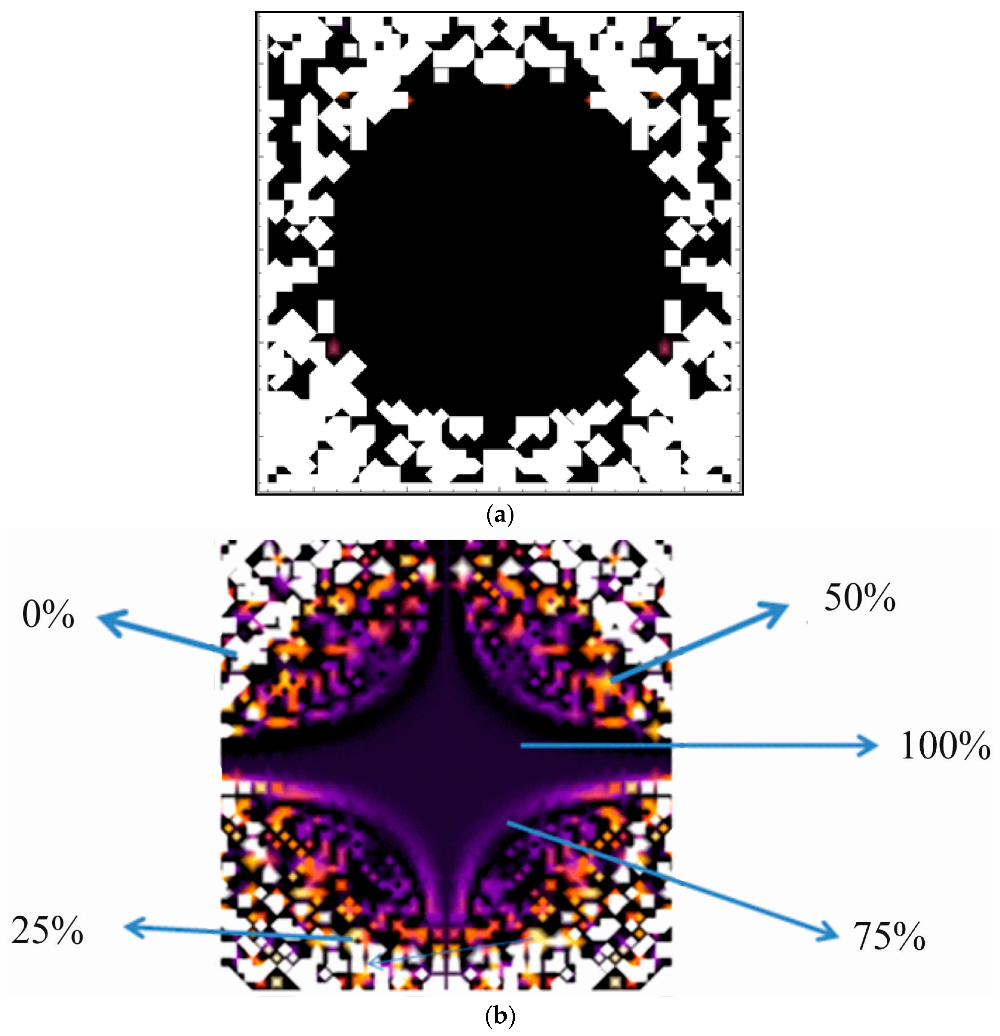
Figure 4 clearly indicates that the CO
2 illumination plays a principal role in the enhancement of the piezoelectricity. It is interesting that the output efficiency was not sensitive to the laser polarizations; however, it crucially depends on the geometry of the treatment. Contrary to the Nd:YAG laser generating at 1064 nm, where we see the different colors (reflecting different signs of laser-induced piezoelectricity changes) for the case of the CO
2 laser treatment, there occurs a huge number of color points. The Er:glass laser treatment gives a picture quite similar to the Nd:YAG laser treatment; because the profile of the photoinduced piezoelectricity is mainly defined by the CO
2 laser illumination.
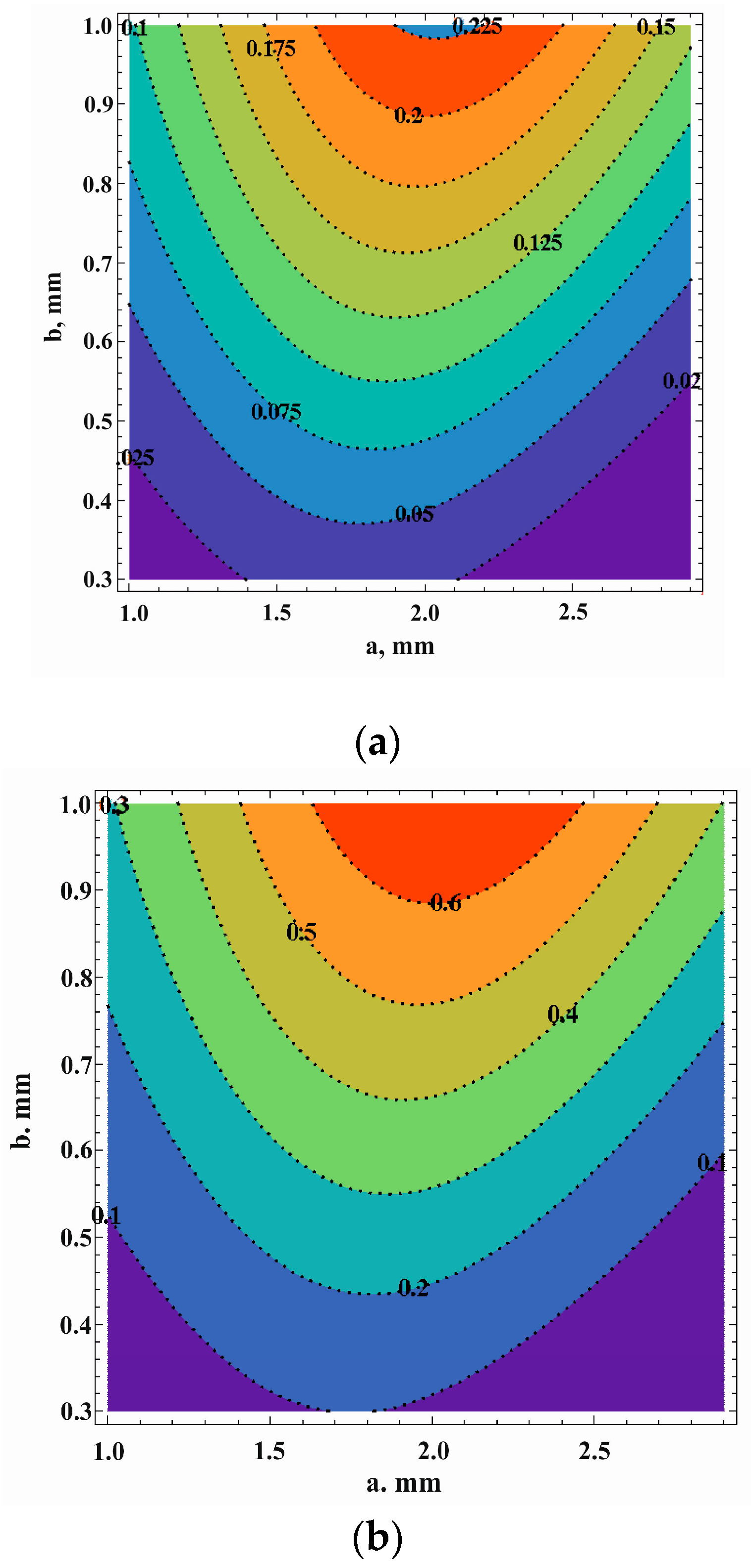
Generally, the pictures show that the photoinduced piezoelectricity has some space non-homogeneity through the illuminated surface. For the case of the lasers that are far from the phonon subsystem, we see more contrast between the maxima and minima of piezoelectricity, and for the Nd:YAG and Er:glass lasers, there exist intermediate values of the piezoelectricity. This may reflect the occurrence of gratings that are sensitive to the contribution of the phonon subsystem. To confirm this prediction, we have performed studies of the space distribution of the diffraction under the influence of the bicolor laser beams (see
Figure 5).
The birefringence for the continuous wave (cw) He-Ne laser beam at 20 mW was detected using the traditional Senarmont method. The principal results confirm an occurrence of the diffraction gratins. Comparing
Figure 4 and
Figure 5, one can see that the sizes of the particular patterns are commensurate for the piezoelectrical and birefringence effects. Therefore, the origin of the piezoelectricity is closely related to the gratings patterns and is closely related to the diffraction-induced birefringence.
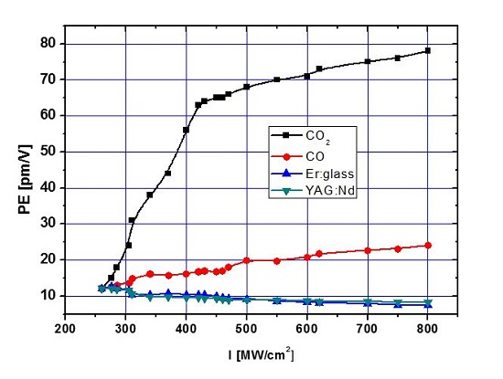
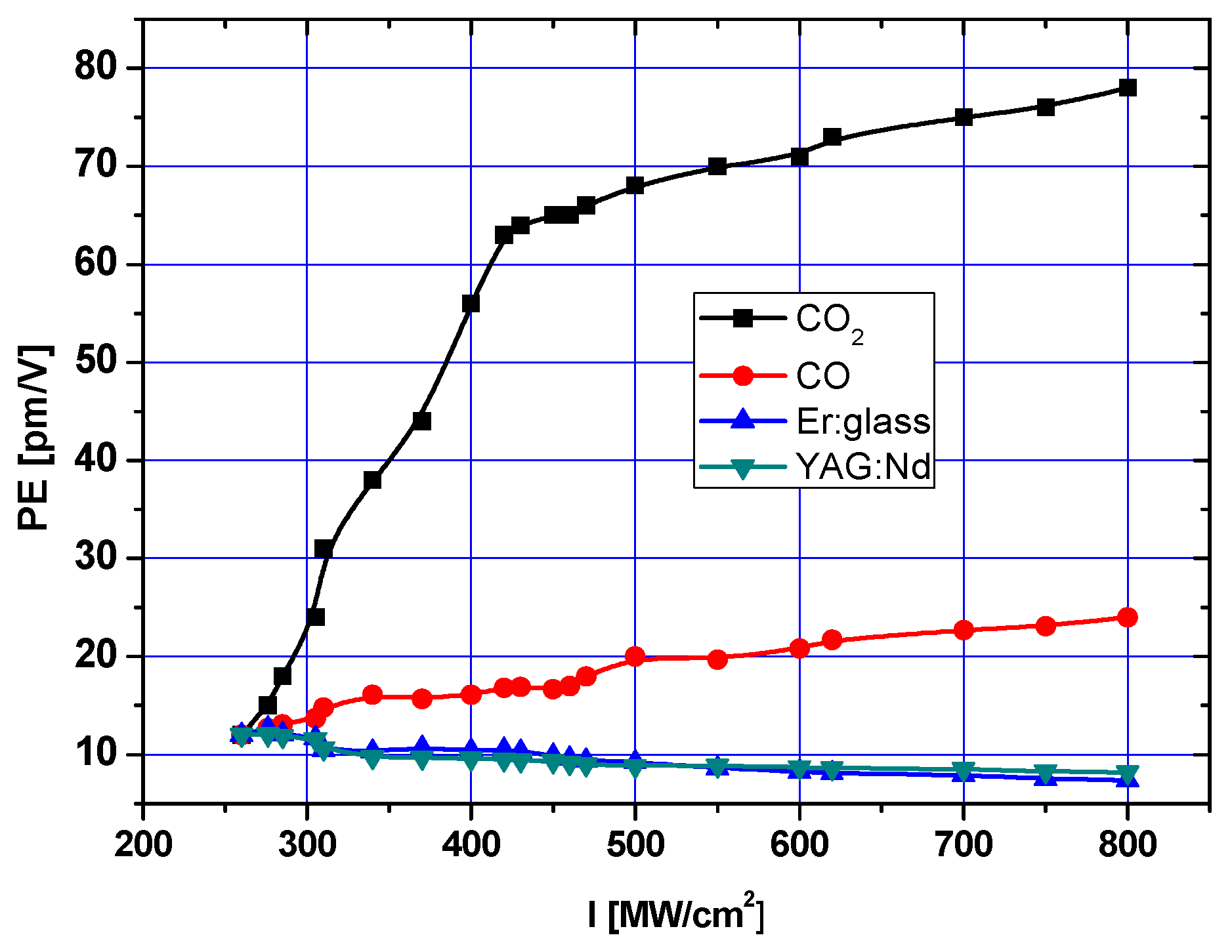
The general view of photoinduced piezoelectricity dependences versus the power densities for the different lasers is shown in
Figure 6. The optimal photoinduced changes were observed at a 50:50 ratio of the particular (fundamental and doubled frequency) intensities for the bicolor treatment, and for the CO
2 laser, the optimal incident angels were equal to about 21–24°. One can see that the maximal piezoelectric changes are observed during illumination by the CO
2 10.6 μm nanosecond laser. The enhancement is very huge: from about 10 pm/V up to about 70 pm/V. The process of the enhancement is non-monotonic versus the pumping powers. At the beginning, it is strongly enhanced with power densities up to about 400 MW/cm
2, and with the further enhancement of the power density, the process is slower with a tendency to a saturation. This may reflect the fact that initially, the principal role is played by photoinduced charge density acentricity with the assistance of the photoinduced anharmonic phonons due to different heating of different specimen’s sides (the latter do not exceed 5–6 K). Additionally, after, the kinetics of the process is saturated showing some destruction of the macroscopical electronic charge density acentricity due to the inclusion of multi-photon excitations. The wavelength 10.6 μm is very crucial here. For example, the CO-induced laser photoinduced bicolor beams at 5.5 μm causes an enhancement by least four-times less. Therefore, one can expect that the primary mechanisms include excitations of the phonon subsystem, including the anharmonic one. Moreover, for the lasers with fundamental wavelengths of 1540 nm and 1064 nm, a substantially different behavior is observed: the piezoelectricity slightly decreases. Therefore, the contribution of the phonon subsystem is less important here. Generally, the processes are a consequence of some competition between the polarizations of the electron subsystem and of the photo-excited anharmonic phonons. An additional role here will be played by free carriers. For this reason, studies of photoconductivity will be given below.
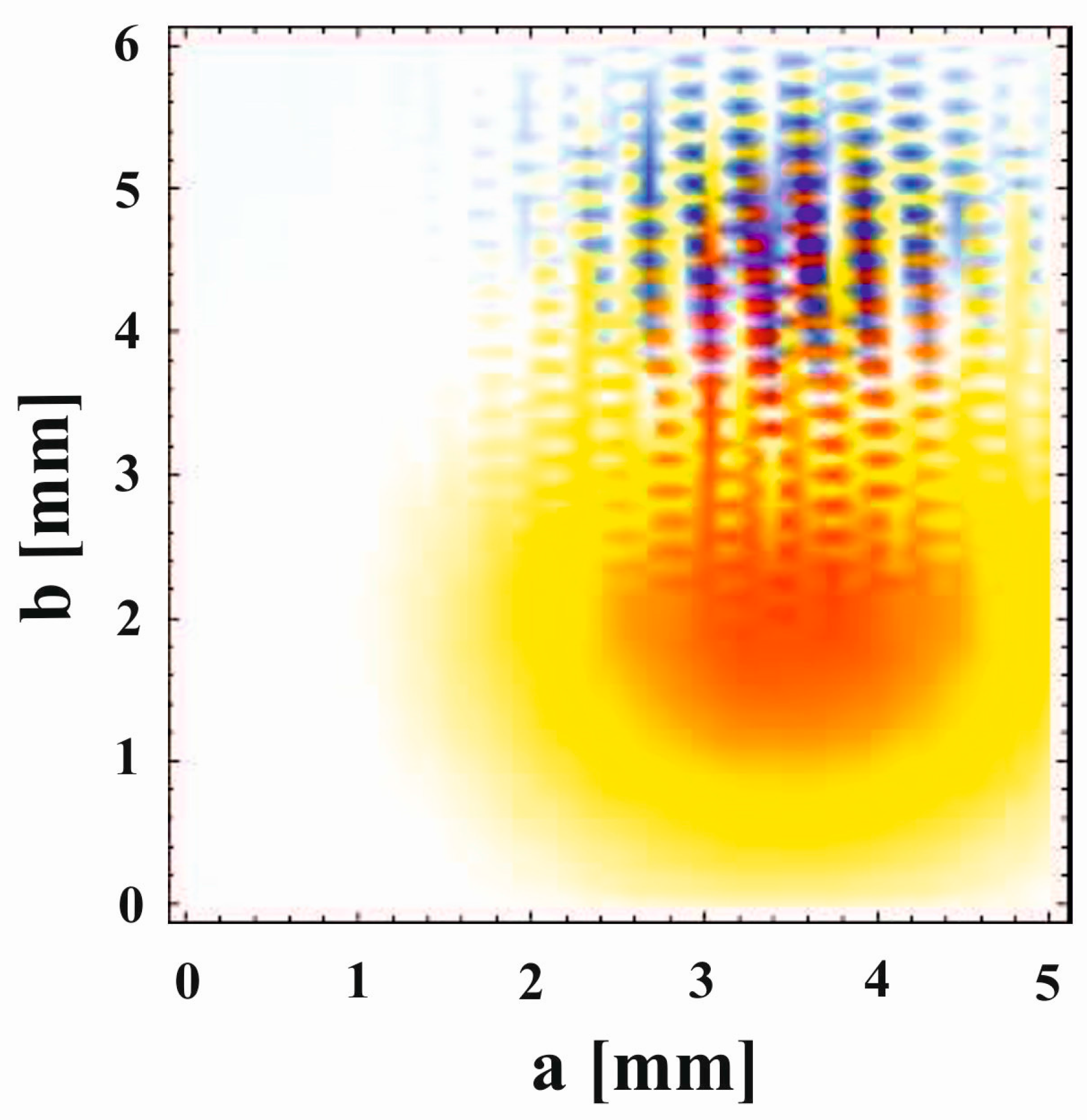
The observed IR-induced gratings (see
Figure 7) confirm that the illumination by two bicolor coherent CO
2 beams at 10.6 μm creates some gratings, the frequency of which is changed depending on the intensity. Therefore, there occurs an opportunity to operate by the space frequency of particular patterns. Additionally, the latter are determined by the photo polarization of the electronic and phonon subsystems. Furthermore, irregular structured patterns are clearly shown, and their periods are changed through the surface. It is interesting that the diffraction disappears within the 10–35 ms after switching off of photoinduced treatment. It is crucial that the irreversible part of the photoinduced changes is almost absent.
Figure 7 clearly indicates that the coherent two-beam illumination at different incident angles is crucially sensitive to the geometry of the treatment. The gratings appearing are closely related to the interactions between the two coherent beams at some angles due to the fulfilling of the phase matching conditions [
18]. Therefore, the angle’s geometry is crucial for the observation of the gratings.
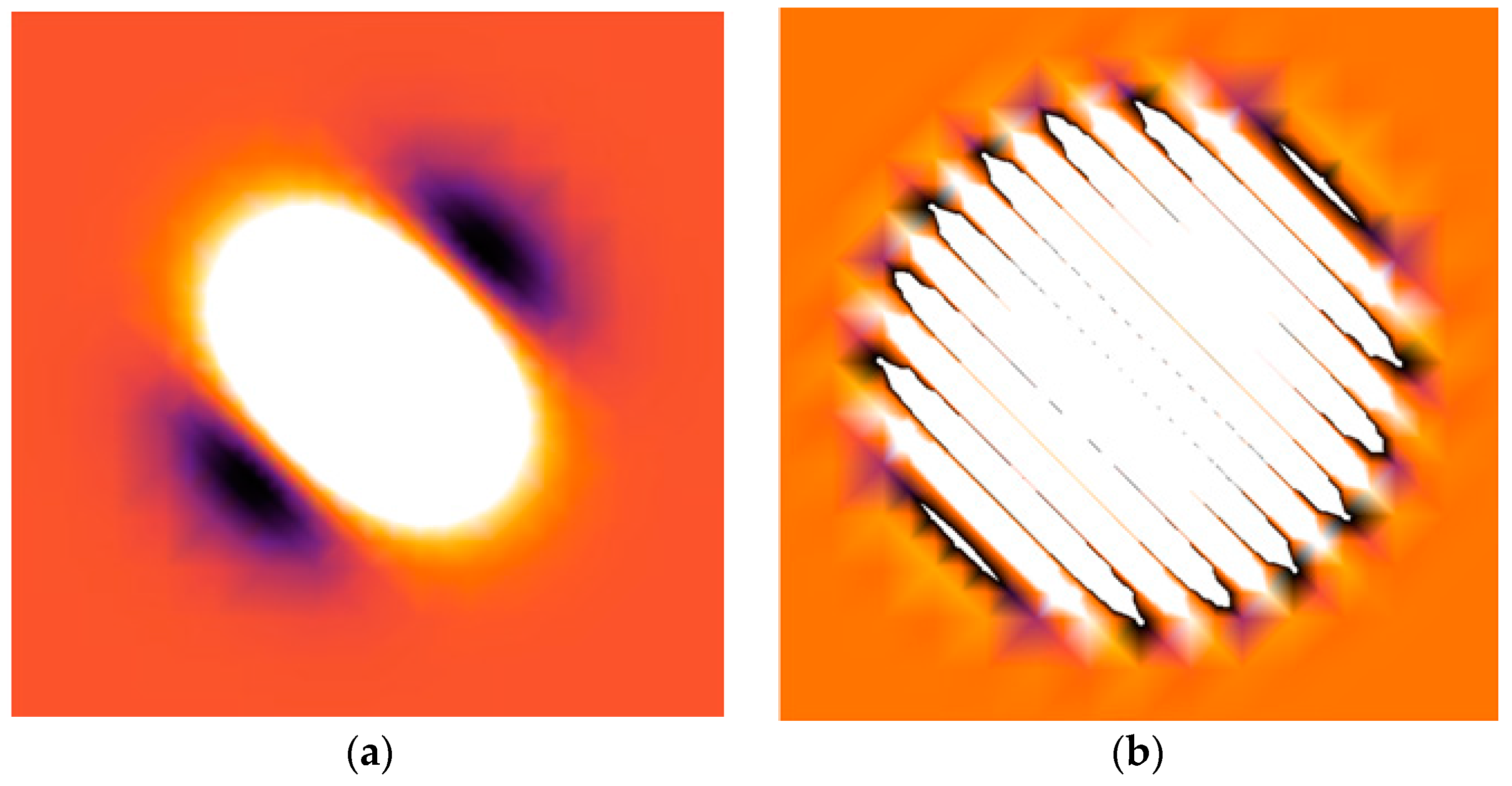
The deep profile control of the photoinduced changes was done by measuring the birefringence perpendicular to the photoinduced beams. It is well known that birefringence is directly related to the anisotropy of the medium. For this reason, the probing He-Ne laser beam at 1150 nm with a beam diameter of about 0.1 mm was moved perpendicularly to the sample’s surfaces. The experiments have shown that the birefringence profile is crucially dependent on the depth of the penetrating photoinduced light (
Figure 8).
To explain the observed differences on the profile distribution obtained at different power densities corresponding to saturation (about 3 s), we have performed additional studies of the photoconductivity, because the photo carriers may play here crucial role.
To avoid the contribution of the photo-thermal changes, we have controlled the temperature changes, which do not exceed 6 K. This corresponded to changes of the birefringence no higher than 0.12.
4. Photoconductivity Features
For photoconductivity measurements, the titled samples were fabricated in the form of parallelepipeds of the grown Ag2Ga2SiS6 samples with sizes ~5 × 3 × 2 mm3. The surface treatment was finally polished using a diamond paste with different grain sizes. For the photoelectrical measurements, the Ga-In electrodes were deposited. The Volt-Ampere control has shown that the contacts are ohmic and non-sensitive to illumination. The photoconductivity studies and their relaxation were measured at T = 300 K. The kinetics of the photoconductivity was monitored after sample illumination, which corresponded to light with a wavelength near the absorption edge. The resistance measurements were carried out by the Keithley 6430 Sub-Femtoamp SourceMeter, (Keithley Products, Bracknell, UK).
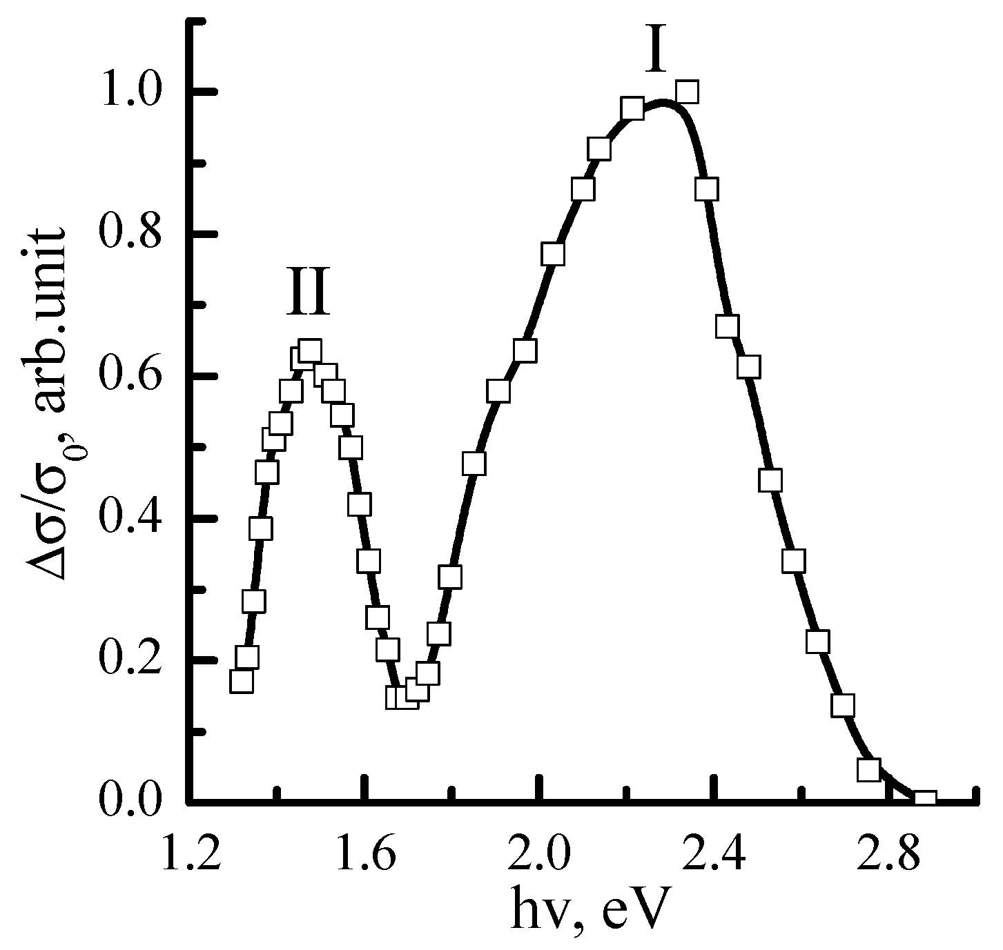
Figure 9 presents the spectral distribution of the photoconductivity for the Ag
2Ga
2SiS
6.
One can clearly see the existence of two spectral maxima of photoconductivity at: hν
1 = 1.47 eV and hν
2 = 2.22 eV. The first maximum is situated near the fundamental absorption edge [
21]. For the compounds with a huge number of intrinsic cationic defects, the required energy for electron transition is at the lower wavelengths. The spectrally-broadened maximum of photoconductivity (1.2–1.6 еV) may confirm the fact that the energy positions of the defects defining the dopant photoconductivity are situated in the middle of the energy gap.
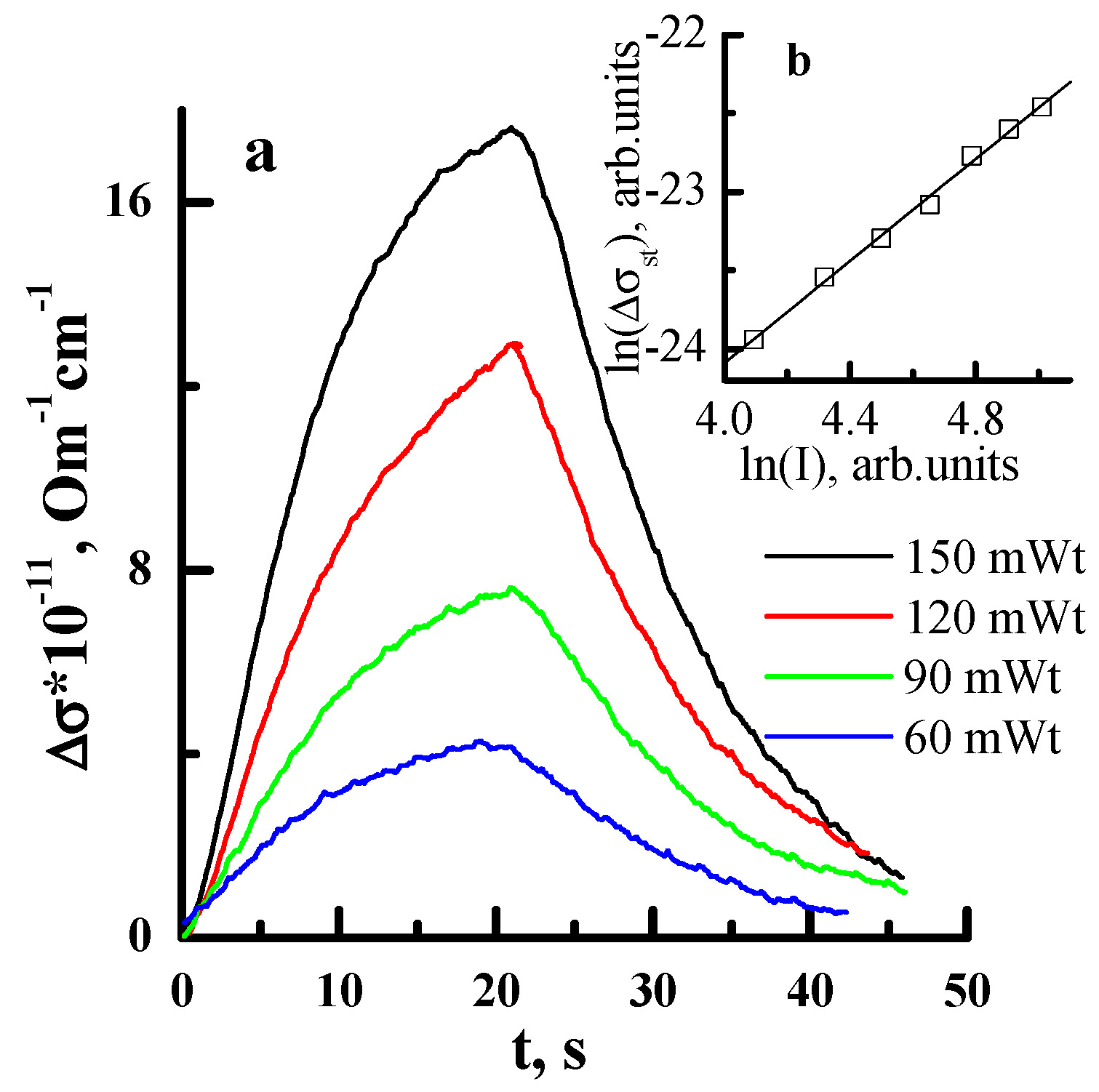
In
Figure 10, the principal results are presented for the photoconductivity kinetics for the crystal Ag
2Ga
2SiS
6 at different excitation intensities. Following
Figure 10, the relaxation kinetics processes are related to long-lived complex features.
At the beginning stage, a deviation is observed from the exponential time dependence of photoconductivity. A more detailed analysis has shown that the photoconductivity arises almost linearly with time. Such behavior following [
22,
23,
24] is observed for heavy doped semiconductors. Lux-Ampere characteristics of the doped photoconductivity at low intensities are almost linear, achieving a saturation at higher intensities. The measurements of the relaxation photoconductivity are done in the range of linear lux-Ampere features.
Following [
24], there exist two complementary models for the long-time relaxation of photoconductivity. The first one is based on the trapping of non-equilibrium carriers by highly localized states near the localized dopant levels with shallow energies within the energy gap. The second model is based on the space distribution of electrons and holes separated by potential barriers, which are caused by space non-homogeneities. As a consequence for the tunneling of electrons in the hole regions, it is necessary to penetrate through this potential barrier, which is a consequence of the recombination. Such a mechanism leads to the slowing of the recombination processes for free carriers.
Following [
25], it is well known that during photo-excitation of the doped levels, these processes are described by the equations:
where
τ1 is the relaxation constant during enhancement;
τ2 the relaxation constant p; Δ
σst the stationary non-equilibrium conductivity.
The relaxation times were determined from linear fittings of kinetics in the scale: (for enhancement) and (for relaxation). Additionally, the times (τ1, τ2) were determined. Following the performed calculations, the magnitudes of τ1 and τ2 are equal to: 6.02 s and 10.22 s; 6.70 s and 10 s during illumination by an 808 nm wavelength with powers of 150 mW and 60 mW, respectively. The relatively huge magnitudes of τ1 and τ2 may indicate the participation of shallow levels or recombination barriers in the relaxed photoconductivity and some role of the interactions with the phonons.
Therefore, these carriers may play a principal role in the photoinduced kinetics of the piezoelectricity. The existence of the two kinds of photoinduced gratings kinetics may also partially be explained by these two relaxation times in the photoconductivity.
5. Conclusions
For the first time, a huge increase of piezoelectricity was achieved for Ag2Ga2SiS6 crystals during illumination by two coherent beams of the photoinduced microsecond CO2 laser generated at 10.6 μm. We have established that maximal piezoelectric changes are observed during illumination by the CO2 10.6-μm illumination with respect to the CO, Er:glass and Nd:YAG bicolor laser treatment. The piezoelectricity enhancement is observed from about 10 pm/V up to almost 70 pm/V. The process is non-linear with respect to the photoinduced light power density. At the beginning, it is strongly enhanced with power densities up to about 400 MW/cm2, and with the further enhancement of the power density, the process is slower with a tendency to a saturation. This may be explained by the fact that initially, the principal role is played by photoinduced charge density acentricity, and after, the kinetic process is saturated, showing some destruction of the macroscopical electronic charge density acentricity due to the occurrence of multi-phonon excitations. The signs of the photoinduced piezoelectricity also are very crucial to the spectral positions of the photoinduced lasers with respect to the main phonon resonances. The wavelength of 10.6 μm is very crucial here. For example, the CO-induced laser photoinduced beam causes the corresponding increase of at least four-times less. Therefore, one can expect that the primary mechanisms include the excitations of the multi-phonon subsystem. Moreover, it was found that the occurrence of the gratings is closely related to the interactions between the two coherent beams at some angles corresponding to the phase matching conditions. The existence of two ranges of photoinduced kinetics may indicate the participation of two carrier mechanisms, which is confirmed by the photoconductivity measurements.


