
Optimizing Tunable LC Devices with Twisted Light
by
 , , , and
José M. Otón
1,*,
Javier Pereiro-García
1,
Xabier Quintana
1,
Manuel Caño-García
1,
Eva Otón
2 and
Morten A. Geday
1 1
CEMDATIC, ETSI Telecomunicación, Universidad Politécnica de Madrid, Av. Complutense 30, 28040 Madrid, Spain
2
Institute of Applied Physics, Military University of Technology, ul. Gen. S. Kaliskiego 2, 00-908 Warsaw, Poland
*
Author to whom correspondence should be addressed.
Crystals 2024, 14(1), 16; https://doi.org/10.3390/cryst14010016
Submission received: 8 November 2023
/
Revised: 24 November 2023
/
Accepted: 21 December 2023
/
Published: 24 December 2023
(This article belongs to the Collection Reviews in Liquid Crystals)
Abstract
:Tunable circular devices made of liquid crystals or other materials, like lenses, axicons, or phase plates, are often constrained by limitations in size, tunability, power, and other parameters. These constraints restrict their use and limit their applicability. In this review, a thorough study of the use of light’s orbital angular momentum in the manufacturing of liquid crystal (LC) devices is presented. Twisted light fosters the simultaneous optimization of most critical parameters. Experimental demonstrations of the unmatched performance of tunable LC lenses, axicons, and other elements in parameters such as lens diameter (>1″), power and tunability (>±6 diopters), fill factor (>98%), and time response have been achieved by reversible vortex generation created by azimuthal phase delay. This phase delay can eventually be removed within the optical system so that lens performance is not affected.
1. Introduction
Liquid crystal (LC) devices, well known for their consumer applications like TVs, monitors, and smartphones, have shown a permanent increase in the number and relevance of their practical applications aside from displays in the past two decades. These non-display liquid crystal devices (NDLCDs) have been extensively studied in many research centers since a remarkable number of new uses are continuously being found.
Regarding their structure, NDLCDs can be roughly classified into two broad groups: those with a large number of pixels (>105) with constant shape, distributed in a regular matrix, usually driven by active-matrix electronics, and those with a moderate number of pixels (say, <103) with arbitrary shape, usually driven by external drivers on passive matrices.
The most common NDLCD with a high pixel number is the spatial light modulator (SLM). It has essentially the same structure as a display, usually employs multiplexed addressing like displays, and can work either in transmissive or reflective mode (e.g., liquid crystal on silicon (LCoS)) like displays. SLMs can be addressed electrically or optically [1] (EASLM and OASLM, respectively). Although OASLMs are usually not pixelated, EASLMs can be assimilated, considering their size, to high-resolution projection displays (the terms are often interchanged). The main differences are the lack of polarizers and the maximum induced phase delay, which is usually above 2π in EASLMs and just π in displays.
SLMs have found plenty of applications [2]. OASLMs can be used for real-time object recognition by optical correlation [3], whereas EASLMs are employed in a plethora of dissimilar systems. To name a few, optical switching [4] and wavelength-selective switches (WSSs) [5] are key in optical communications, while computer-generated holography [6], adaptive optics [7], optical Fourier neural schemes [8], and optical computing [9] are applied to many fields, including hot topics like artificial intelligence [10].
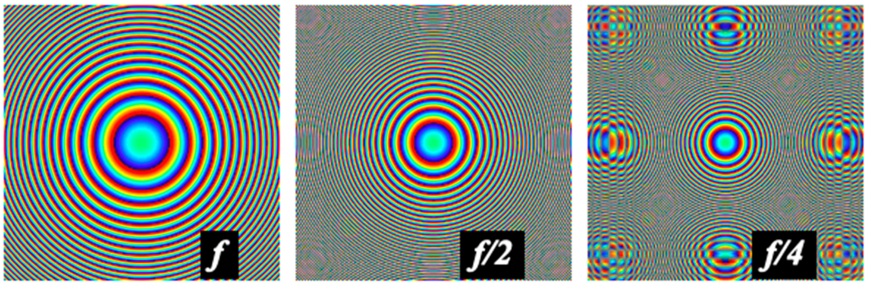
Nevertheless, SLMs also feature some drawbacks. They are expensive for many consumer photonics applications, have low light efficiency—mostly due to the active-matrix electronics shadowing the pixel area and reducing the fill factor—and may show diffraction and aliasing issues (Figure 1) when dealing with high-resolution patterns [11]. It should be mentioned that the ring thickness of Fresnel lenses decreases as the distance from the center increases; this is the reason the aliasing artifacts show up at the edges.
A second group of NDLCDs relies on a low number of pixels, perhaps tens or hundreds, whose shape is precisely designed for the application specifications. Moreover, they are usually driven by external electronics so that the active area is free from spurious shadowing components. Thus, the two main shortcomings of SLMs are avoided in a single action: the fill factor is increased considerably, and aliasing is completely avoided.
These low-resolution passively addressed NDLCDs can, in turn, be divided into two families: those adopting a periodic linear shape and those with a circular shape and often circular symmetry. The devices of the first group usually behave as diffraction gratings, e.g., POLICRYPS [12] or sawtooth gratings that can be used as beam steerers [13]. Circular devices are perhaps the most important group of NDLCDs from the application side. This group includes axicons [14], optical vortex generators [15], and the ample family of tunable lenses.
At present, LC lenses are finding applications in many dissimilar fields, such as vision (e.g., eyeglasses [16], contact lenses [17], and intraocular lenses [18]), adaptive optics for astronomy [19], or wearable devices [20], in addition to their traditional applications as tunable lenses for consumer photonics [21,22].
Although not included in LC lenses, it is worth mentioning the recent interest in liquid or optofluidic lenses controlled by magnets [23] or piezoelectric devices [24]. These are currently being offered as an alternative for tunable lenses in smartphone objectives [25].
Low-resolution, passively addressable NDLCDs are also not without their drawbacks. The most relevant is the low power achieved by LCs with moderate birefringence. The deviation angles of beam steerers are small, and the power of manufactured lenses and axicons is low.
As shown in the next section, possibly the best way to overcome this obstacle is to employ tunable structures (prisms, lenses) based on Fresnel geometries. Nevertheless, these structures create, in turn, additional problems mainly related to addressing.
In this work, a global solution to the problems derived from Fresnel geometries in circular structures, such as axicons and lenses, is described. The combination of structures with radial and azimuthal birefringence gradients produces devices with a significant increase in crucial characteristics such as diameter, fill factor, or power while maintaining simple addressing geometries. High-power, large-aperture lenses with nearly 100% fill factor are demonstrated.
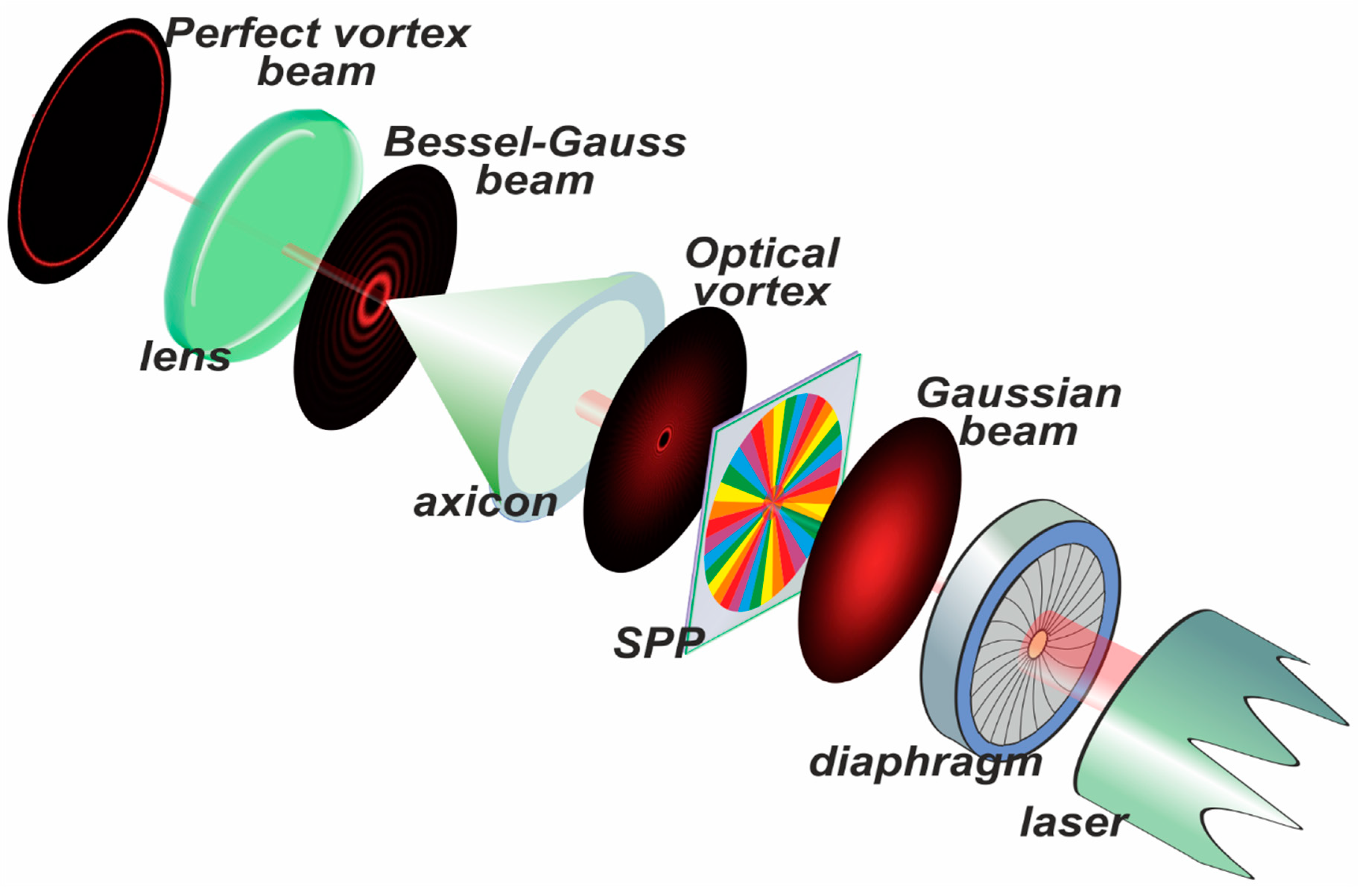
The proposed structures are based on two key components: Fresnel structures and elements with variable azimuthal phase delay, which bestow orbital angular momentum (OAM) to the impinging light. OAM generates optical vortices that can be advantageous in certain structures, like optical tweezers. Otherwise, they can be removed at a later stage. To adequately describe the devices, therefore, it is advisable to review these structures and elements.
2. Liquid Crystal Circular Devices
2.1. Liquid Crystal Lenses
LC lenses may be used by themselves or as a supplement of glass lenses, e.g., to tune up the power of the glass lens within a certain range, with functionality equivalent to commercial progressive lenses, but with improved performance since the power of the whole lens is modified by a sensor providing autofocus, as in digital cameras.
2.1.1. Graded Index Lenses
Let us design a flat–convex convergent thin lens (paraxial approximation). A fixed lens can be made with a flat–convex glass whose thickness is determined by the desired power in diopters (the inverse of focal length). A tunable lens can be made with a flat liquid crystal cell (graded index or GRIN lens, Figure 2), achieving a switching profile across the cell that mimics the glass profile in terms of the optical path, , the refractive index, and the physical path.
A lens is formed when the optical path along the lens radius decreases quadratically with distance from the center. Both the refractive index (birefringence, ) or length (lens thickness, ) can be varied to achieve optical path variation. Glass lenses vary the glass thickness, while liquid crystal lenses vary the refractive index:
Theoretically, both mechanisms are equivalent; however, this is not the case in working conditions. Let us assume we want to manufacture a 1 cm flat–convex lens with a power diopters (i.e., a focal length F = 20 cm). The curvature R2 of the glass lens can be calculated to within a thin-lens approximation using the lensmaker formula [26]:
Assuming and (air), the curvature cm. If the lens has a diameter of 1 cm, then the thickness of the lens (strictly, the difference between the thickness at the lens center and its borders) is 0.125 mm, which can be easily fabricated.
2.1.2. Designing LC Lenses
In liquid crystal cells, the situation is different. A quadratic index profile is required, as above; moreover, the profile must be variable so that the lens can be tunable. Several solutions have been proposed to achieve this quadratic profile with adaptive focus:
- Zonal or pixelated lenses generate the quadratic index profile through independent electrodes. SLMs can be used to make such lenses; however, it is usual to employ pixels shaped as concentric rings [27].
- Modal lenses can produce smooth profiles without pixelization, with just one continuous electrode or a few of them at most. The electric field distribution—hence the index profile—is achieved by employing high-resistivity electrodes, usually between 100’s □ and some □. High-resistivity electrodes can be made of several materials, such as poly(3,4-ethylenedioxythiophene) polystyrene sulfonate (PEDOT-PSS) [28] or ultrathin indium–tin oxide (ITO) [29].
- The high-resistivity electrode behaves as a transmission line [30], and the profile can be modified by varying the voltage amplitude and the frequency, therefore making it possible to create radial voltage gradients that follow up the required quadratic index profiles for lenses or other profiles for different optical elements, e.g., axicons. Modal control has also been proposed in the Fresnel lens [31], which will be commented on below.
- A rather different approach is given by Pancharatnam–Berry phase devices (PPD, [35]), specifically Pancharatnam–Berry lenses. PPDs are elements in which electromagnetic waves undergo continuous phase changes due to a continuous change in the material through which they are passing. Typically, liquid crystal PPDs work by smooth variations of the alignment directions on both the confining surfaces of a retardation liquid crystal cell, i.e., introducing a fixed linear retardation with variable azimuthal angle.
Such a PPD inverts the handedness of incident circularly polarized light and introduces a relative phase delay depending on the local alignment direction of the waveplate, as will be discussed below. These devices and lenses have a wide range of applications with a spatial phase variation pitch beyond anything achievable in conventional SLMs or ITO-based devices [36,37].
However, unless special effort is invested, the devices will have opposite behavior for the two-handedness of circularly polarized light, which makes them “unstackable” and typically only provide an ON–OFF switching behavior optimized for a single wavelength. Thus, the main drawbacks of PPDs are their deficient tunability and their strong dependence on the wavelength of impinging light [38].
Nonetheless, the lens power achieved by regular materials (except PPDs) is quite modest. The quadratic index at a given distance from the center is defined as
where is the refractive index at the lens center
where is the angle between the LC optic axis and the direction of light propagation [39]. can reach the extraordinary index ; is the ordinary index at the cell edges (we are considering a convergent lens), and is the cell radius. It can be easily shown by geometrical considerations [40] that the power of a thin LC lens with quadratic index profile is
where is the LC cell thickness, , and is the focal distance. This dependence on the square of the radius is critical for LC lens performance. A typical LC has a birefringence (BR) around . Using the same 1 cm lens above in an LC cell of standard thickness (e.g., 8 µm) and assuming the maximum BR is achieved, the power yielded by the LC lens is as low as 0.13 diopters.
Clearly, the problem arises from the low phase delay induced between the center and the edges of the LC lens. According to the delay formula
Assuming reaches , the induced delay is 5.82π in the green region (550 nm) and 5.06π in the red region (633 nm). This is more than enough for applications such as displays or phase gratings but too small for lenses or beam steerers.
2.1.3. Increasing LC Lens Power
Several solutions have been proposed to overcome this problem [41]:
- Use of high-birefringence LCs [42]. This can be helpful, but it is not a solution by itself. At present, high-BR mixtures are in the range of 0.4–0.5, which would double or triple the lens power at most.
- Increase of the cell thickness. LC cell thicknesses above 100 µm driven by ultrasounds have been proposed [43]. For electrically driven cells, however, thickness is severely restricted—usually to 20–30 µm—by response-time degradation and poor material orientation in thick cells. Again, alternative solutions, including dual-frequency nematics [44] and polymerization [45], have been proposed so that the spatial orientation of LC molecules is kept and the response time is improved.
- Decrease of the cell radius. This would alleviate the strong dependence that thwarts the lens power. A diopters lens of 1 cm diameter, like the above glass lens, would require an LC thickness of 314 µm, which would be impossible to control or orient with standard fabrication procedures. (Unsurprisingly, this is the thickness difference required for the glass lens, where its refractive index is 1.2 rather than 1.5, i.e., ). If the LC lens diameter is set to 2 mm, then the required LC thickness is 12.5 µm, a perfectly feasible value. Many groups work on LC microlens arrays [46,47] to take advantage of small diameters while keeping reasonable apertures.
- Creation of Fresnel lenses. Fresnel geometry provides the most powerful solution, capable of producing high-power, high-aperture lenses [48] with outstanding fill factor and excellent time response. This topic is dealt with in the next sections.
2.2. Fresnel Lenses
Fresnel structures offer a radical solution to the problem of low power in lenses and other LC devices at relatively little cost. There is an increase in the complexity of electrode design, and there is an evolution from devices with analog tunability to others where only discrete power values can be selected. Both drawbacks have been overcome, as shown below.
Fresnel structures are based on the concept of phase wrapping: a phase delay of 2π (i.e., a full wave) is equivalent to no delay. It follows that the material producing such delay can be removed without affecting the optical properties of the light passing through the structure. Removing material may produce a dramatic decrease in the device thickness, making it possible for regular LC samples in the 10’s µm range to develop lens powers of several diopters. Moreover, the lens aperture does not need to be reduced.
2.2.1. Types of Fresnel Lenses
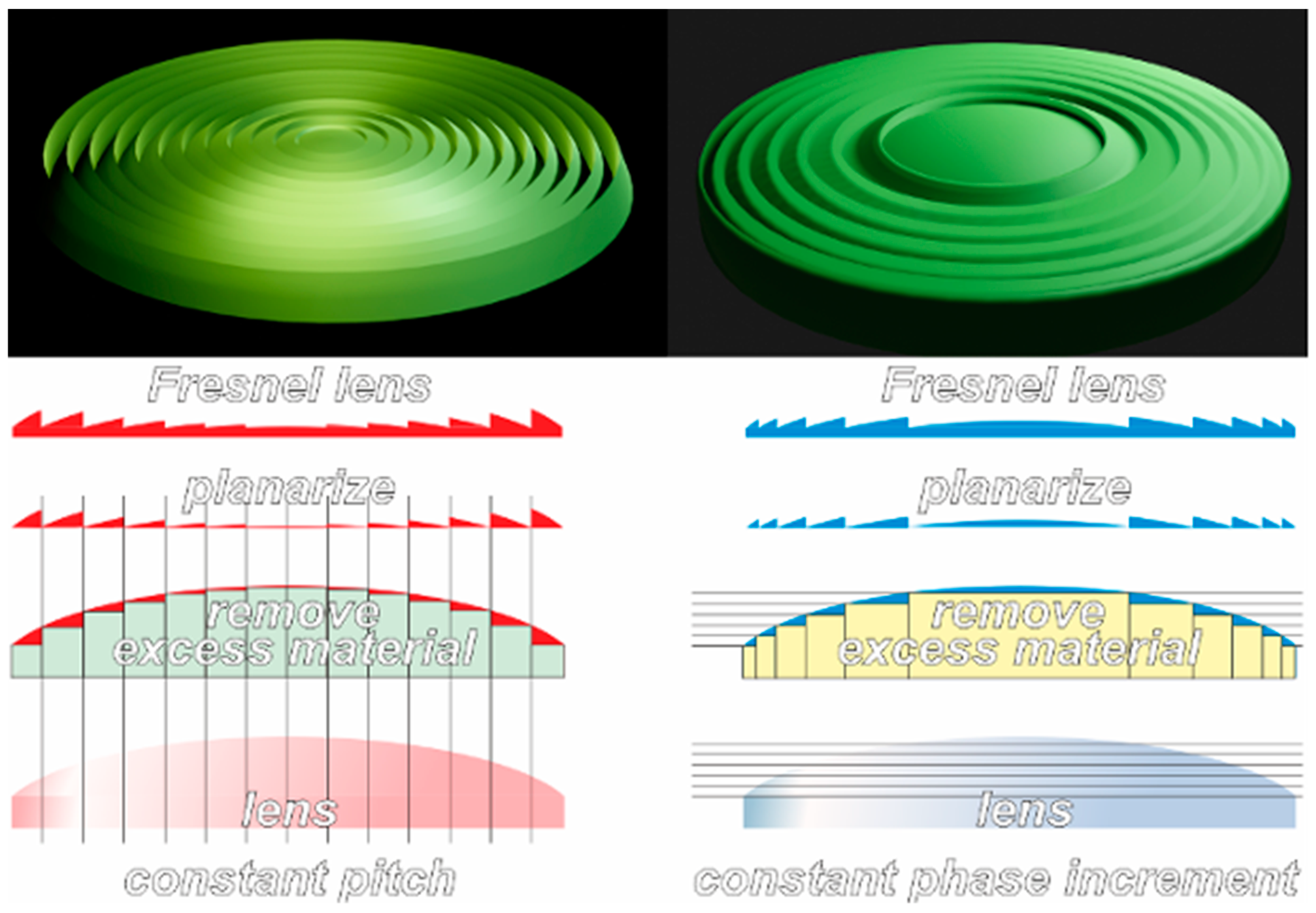
There are two basic designs of Fresnel lenses (Figure 3). In the first one, the lens section is cut into several slices of the same thickness parallel to the optic axis. The excess material is removed, and the remaining segments are aligned on a line. The Fresnel lens is generated by rotating the obtained profile about the normal axis. This was the preferred configuration in the Fresnel lens for lighthouses.
In the second version of the Fresnel lens, the lens is cut into parallel sections of the same thickness. Each section produces a delay that is an integer multiple of the first section. Excess material is removed and processed as in the previous case. In the first case, the pitch of the sawtooth is kept constant; in the second, the delay increment induced in each section is constant, but the pitch is variable. This is the solution usually adopted by LC Fresnel lenses since inducing the same delay is often equivalent to applying the same voltage, thus simplifying the drivers.
2.2.2. LC Fresnel Lenses
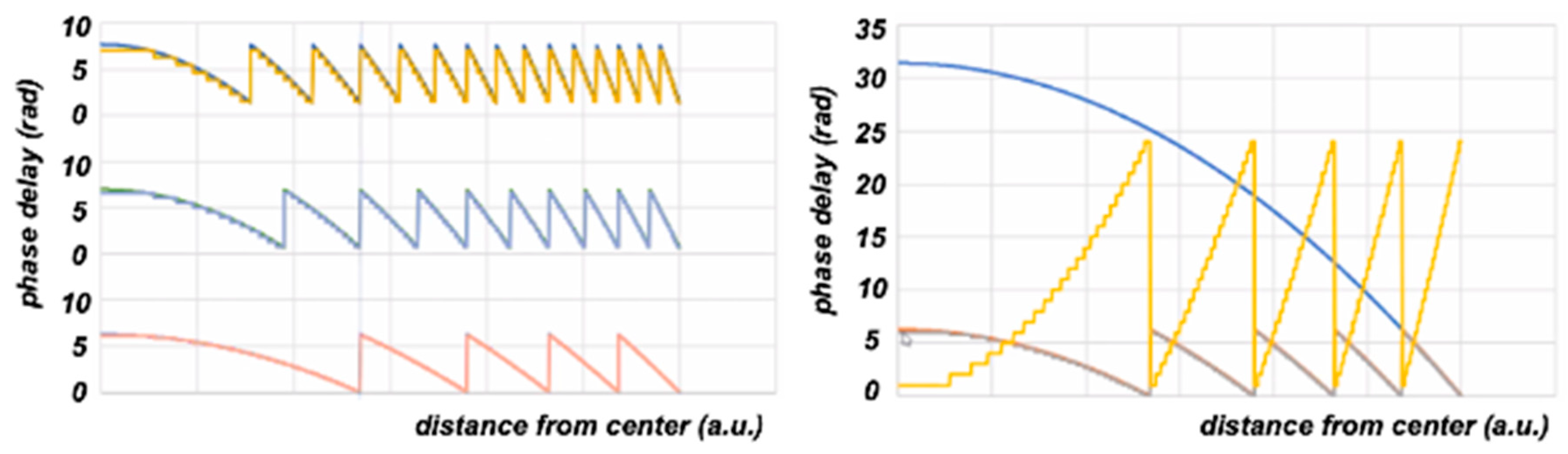
In the examples shown in Figure 4, a 2π delay per ring is used. The lens power can be modified, inducing a multiple of 2π on each ring. The phase delay on each ring can be set to any multiple of 2π limited to the LC thickness and birefringence.
The lens power can also be modified (Figure 4, left), defining each ring with an arbitrary constant number of electrodes, thus increasing or decreasing the number of rings in the lens. The limit is the number of electrodes: theoretically, one can define a ring with just two electrodes set at 0 and π delay (the next 0 delay would be wrapping the 2π delay). Nevertheless, the quality of the lens significantly degrades when the number of electrodes defining each step decreases to low values.
In Fresnel LC lenses, the lens power of Equation (5) becomes
where is the number of Fresnel rings, and is the number of 2π’s (or ’s) delayed by each ring. Taking the same parameters as in the example above, at 550 nm. Using a Fresnel lens of 7 rings, the lens power diopter. The abovementioned lens of 5 diopters would require about 37 rings or a reduction of the lens diameter to about 4.6 mm while keeping the same 7 rings.
In the simplified example of Figure 4 (right), an LC Fresnel lens of five 2π rings is modeled. Each ring is defined by 24 electrodes with different widths (yellow curve). The rings have different widths as well. The brown curve shows the phase delays induced by each ring (up to 2π or 6.28 rad). The blue curve is the total delay achieved within the lens (10π or 31.4 rad) without considering phase wrapping.
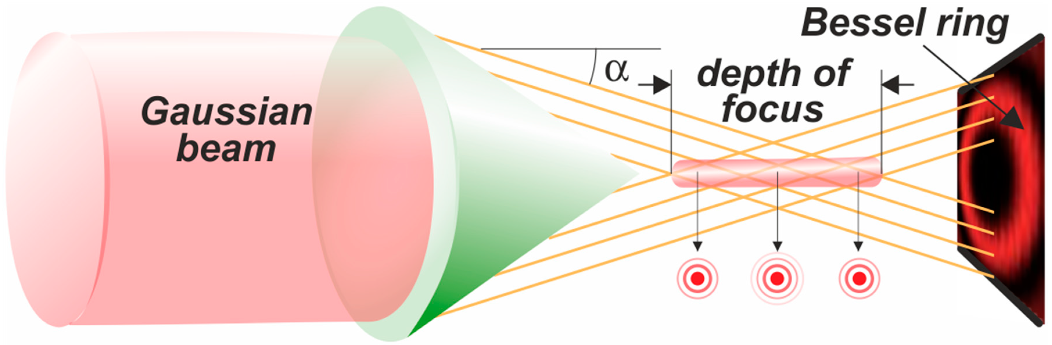
Axicons are special lenses whose surface is a cone rather than a parabolic profile. As such, all light rays impinging an axicon in the same section plane are bent parallel to each other (Figure 5). Contrary to lenses, the rays do not focus on a single point but on a line (like Star Wars laser sabers) called depth of focus (DOF). DOF length depends on the angle of the cone generatrix and the refractive index of the material.
2.3. Axicons
If a Gaussian beam impinges an axicon, the beam adopts the shape of a non-diffracting zero-order Bessel beam. These beams are characterized by an intensity pattern with concentric circles, where the size, shape, and intensity of the central spot do not vary with distance within DOF. Beyond DOF, the Bessel profile becomes a ring, with the wavevectors of the Bessel beam propagating in a conical pattern.
The DOF length can be calculated [49] from these wavevectors and their radial components
where is the diameter of the incident Gaussian beam, and the angle is defined in Figure 5. Typically, the DOF is 10× longer than a Gaussian waist of the same diameter.
Axicons have found several applications derived from the peculiar shape of the output beam [50]. They have been proposed for optical tweezers [51] and atomic traps [52]. In telescopes, the spherical objective can be replaced by an axicon [53]. They also have applications in laser eye surgery [54]. Combining concave and convex axicons, the diameter of the light beam ring can be tuned.
Like lenses, axicons based on liquid crystals can be manufactured. The cone angle (equivalent to the lens power) can be increased by employing Fresnel structures. The approach is identical to that of the lenses, with the only difference being that all axicon rings are equidistant and have the same amplitude.
Axicons are closely related to vortices, which are commented on in the next section. Diffractive spiral axicons (DSA) have been recently proposed [55] for the generation of Perfect Vortex Beams (PVB).
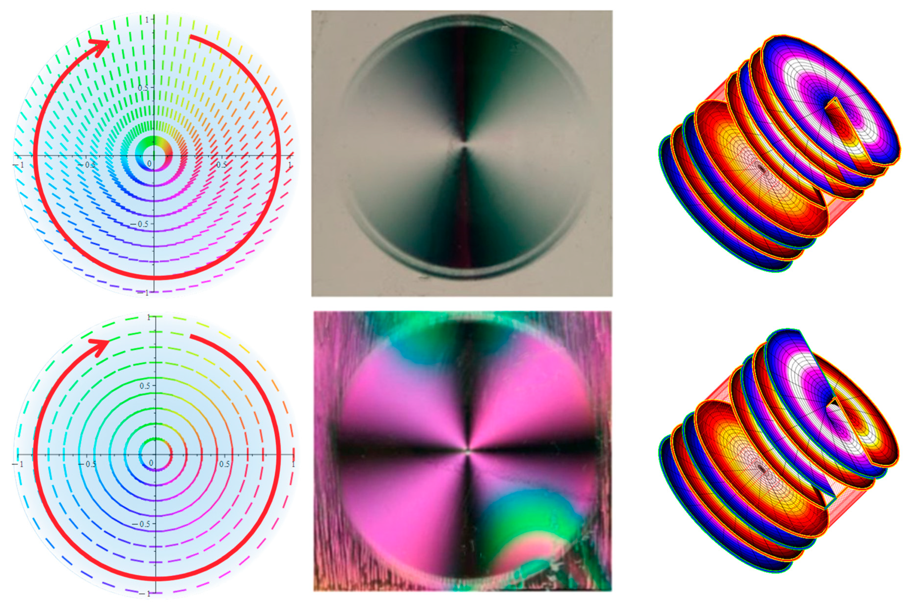
2.4. Vortices
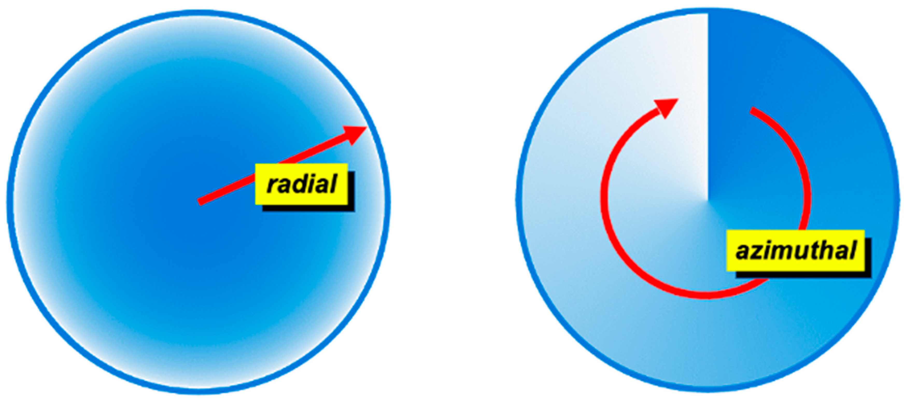
A vortex beam is a light beam with a phase singularity at the center [56]. The beam has azimuthal rather than radial phase variations (Figure 6) in such a way that a full rotation corresponds to a phase shift multiple of 2π. This multiple of 2π is called topological charge, ; it can be positive or negative depending on the rotating sense of the azimuthal phase variation.
At the center of the structure, all phases would theoretically meet; light cannot carry any power under these conditions. Therefore, the singularity appears as a black dot in any vortex structure. This poses an additional difficulty to the use of vortices in complex phase optical systems. Fortunately, the singularity can be wiped out, as shown below.
Nevertheless, there are applications for which the black region generated at the vortex center results are extremely useful. Astronomical coronagraphs are devices able to visualize faint signals located close to bright stars (e.g., exoplanets or brown dwarf stars in binary systems). Several tunable coronagraphs based on liquid crystal vortices have been proposed [57,58]. Terahertz vortex beams have been presented as well [59].
2.4.1. Orbital Angular Momentum and Topological Charge
The spiral wavefront of vortices possesses an orbital angular momentum (OAM) of per photon [60], by which a laser beam can transfer a mechanical torque to suspended particles, inducing a clockwise or counterclockwise rotation depending on the sign of the topological charge.
As well as fundamental physics issues like transferring OAM to matter, even to electrons [61], the OAM could have attractive applications: as OAMs with different topological charges are orthogonal, OAM provides an additional tool for multiplexing optical communications [62], beyond other classical multiplexing techniques such as polarization or time-division. There is no theoretical limit to the number of multiplexed channels; it would just be conditioned by technical issues.
OAM can be applied to other areas, such as micromanipulation, particle trapping, and metrology. Some authors [63] have suggested converting OAM into twisted excitons to employ them in quantum information processing. Optical vortices, specifically Perfect Vortex Beams (PVB), have unique optical characteristics that make them attractive for material processing and micromachining.
2.4.2. Liquid Crystal Vortices
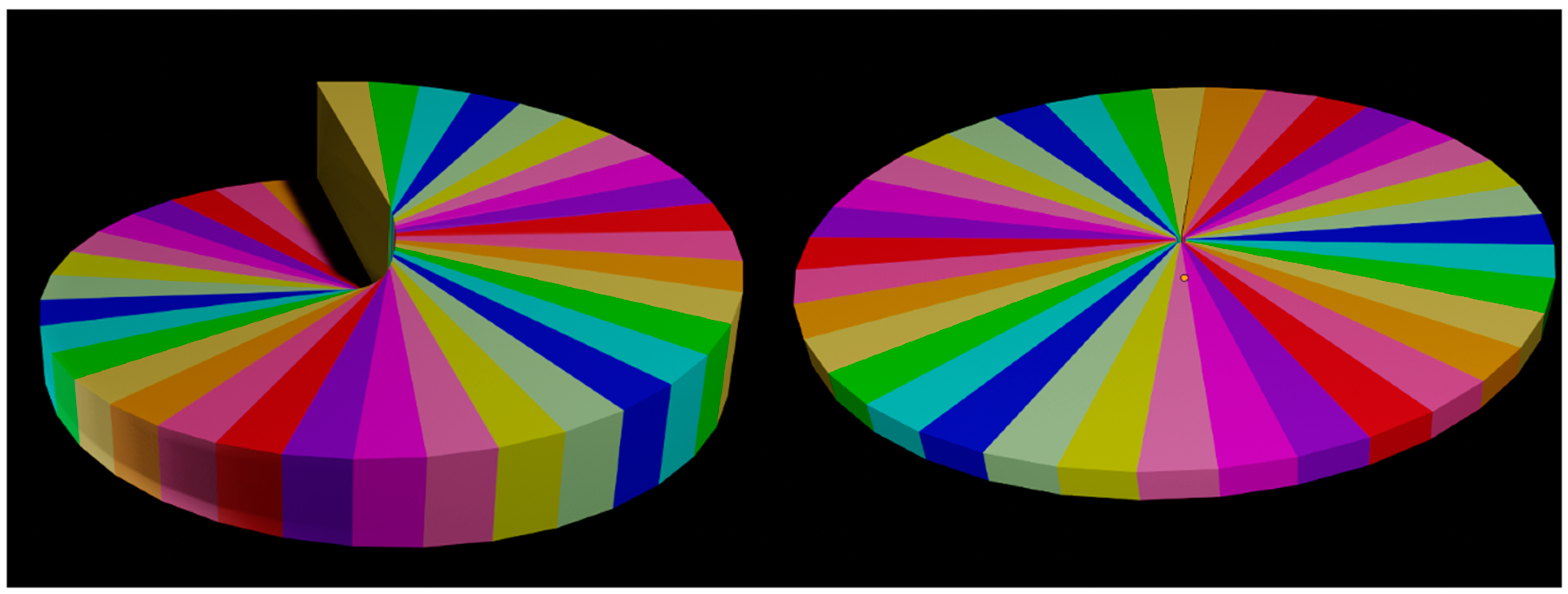
The azimuthal phase variation can be achieved, as in the lens case, by modifying the optical path of the incoming beam across its section. This can be done (Figure 7) by modifying either the thickness of the element in mechanical non-tunable vortex generators or the refractive index of a planar element, as in the case of liquid crystals.
As seen in the figure, the LC optical vortex generator is a spiral phase plate (SPP) made of pixels shaped as pie slices. One can choose the topological charge of the device by assigning a 2π shift to several slices. For example, the right picture of the figure has 36 slices. With this device, one can generate vortices from to (with pie slices assigned to 0 and π alternatively). The higher the topological charge, the more blurred the generated vortex since fewer slices (steps) are used to define every 2π cycle (staircase), and the index gradient profile becomes more jagged and less similar to analog increments.
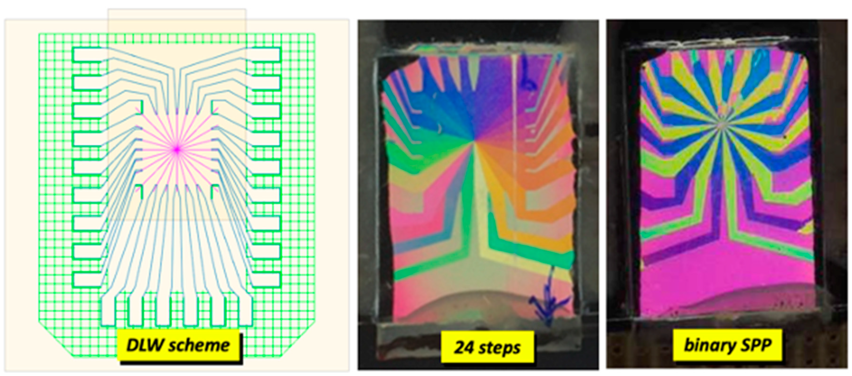
A working prototype of an SPP with a 1 cm active area is shown in Figure 8. The SPP is made of 24 independently driven pie slices. On the left is the planning of the Direct Laser Writing (DLW) scheme for this prototype (DLW is explained in the Spirals section). At the center, a configuration with topological charge , the phase delay increases π/12 radians between adjacent slices. At the right, a binary configuration 0, π, 0, π, 0… with topological charge .
2.4.3. Perfect Vortex Beams
Perfect Vortex Beams (PVB) are beams carrying OAM whose intensity pattern is constant irrespective of the topological charge [64]. Theoretically, PVBs are Fourier transforms of Bessel beams (actually Bessel–Gauss beams). PVBs are non-diffractive, which opens further application possibilities, such as cryptography and imaging.
There have been many proposed schemes for the generation of PVBs. Spiral phase plates and axicons can be used to convert Gaussian beams into Bessel–Gauss beams (Figure 9). Then, a simple lens can transform the Bessel–Gauss beam into a PVB.
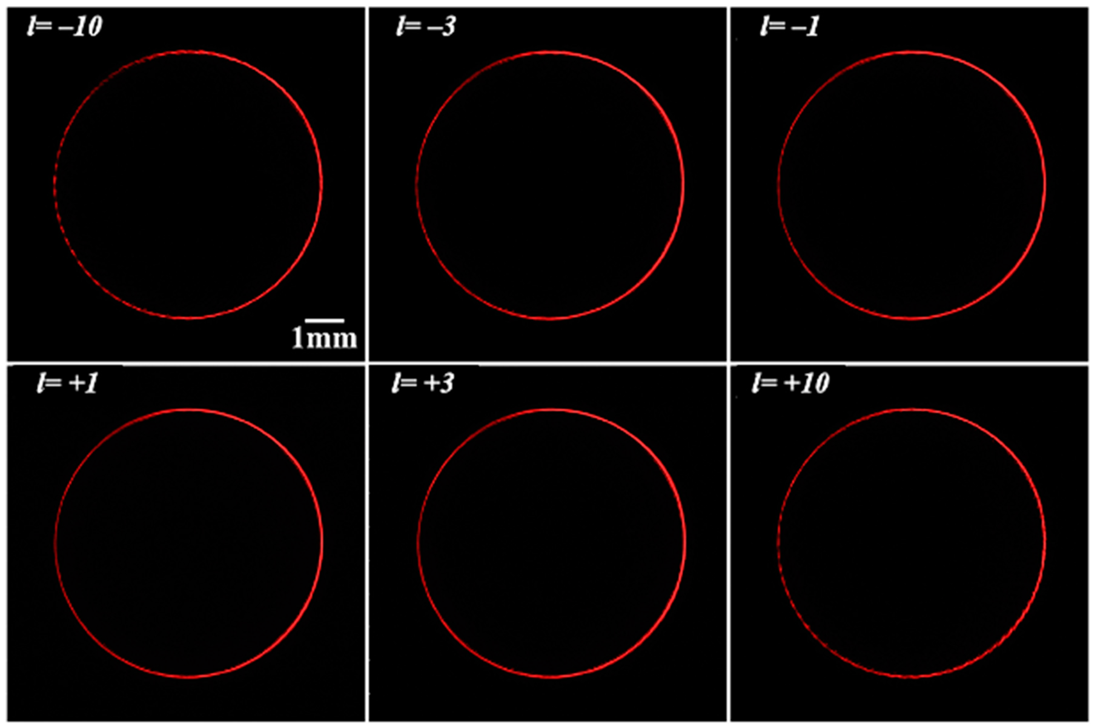
Axicons and spiral phase plates made of flat LC devices have been used to fabricate an optical setup that is able to generate PVBs with variable topological charges [65]. Figure 10 shows a set of PVBs with different topological charges (from to ), obtained with a spiral phase plate of 72 independently driven pie slices. The pictures are substantially identical. Only small discontinuities can be observed in the largest positive and negative topological charges.
2.5. Q-Plates
Unlike the variable linear retarders discussed above, the simplest LC-based Pancharatnam–Berry phase devices (PPD) have a single fixed retardation structure optimized for a single wavelength [66]. A constant retardation is introduced throughout the active area of the device, with an azimuthal variation of the LC alignment, i.e., of the slow axis.
2.5.1. Half-Wave Retardations on Circular Light
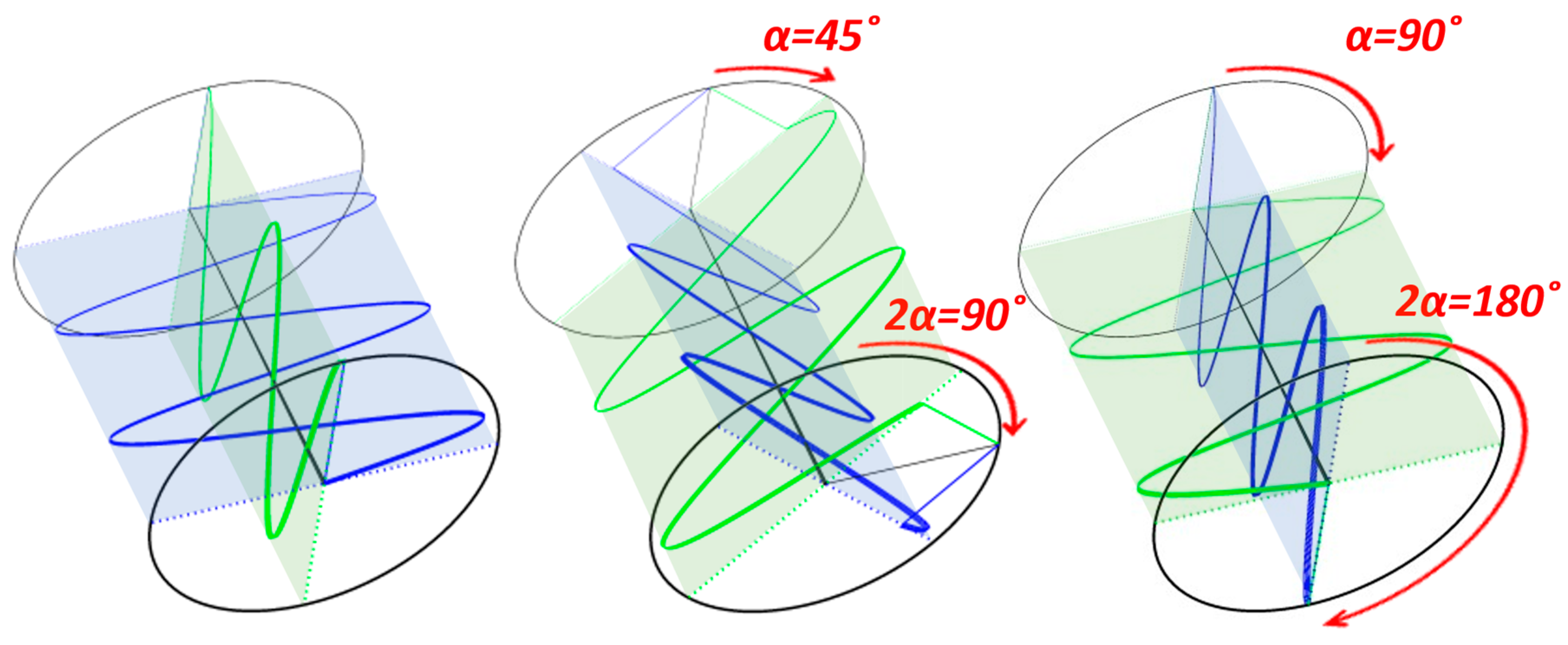
It is well known that a retardation changes circularly polarized light from one hand to another, i.e., right circular polarization (RCP) into left circular polarization (LCP) and vice versa. This causes mirroring of an incident linearly polarized light about the angle between the slow axis and the incident linearly polarized light.
At a given instance, incident circularly polarized light undergoes an inversion of hand, and the output electrical field undergoes a rotation, which is twice the angle between the incident instantaneous electrical field vector and the fast axis of the LC, as indicated in Figure 11. The rotation of the electrical field of a circularly polarized beam is equivalent to a change in phase. i.e., an azimuthal variation of the slow axis of α leads to a relative phase variation of 2α. The sign of the phase variation depends on the handedness of the light.
The same argument could have been made purely with Jones algebra. The optical system consists of a half-wave plate at an angle , which converts the hand of an incident circularly polarized light and introduces a phase delay of .
where and are rotational matrices of and α radians, respectively. As usual in Jones algebra, all the common time and space variations of the electrical field have been omitted.
2.5.2. PPDs and Q-Plates
These PPD structures could be employed to generate so-called Q-plates [67], which convert circularly polarized light of one hand into the other while introducing an angular orbital momentum.
First-order Q-plates are relatively easy to manufacture. Indeed, they can be fabricated by conditioning the aligning surface mechanically. One of the surfaces must induce tangential alignment of the LC about the center of the device. Such alignment is easily achieved by spinning the sample while rubbing or using a power drill for the alignment.
The other surface must induce a complementary radial alignment. This can be done mechanically, too, but it is easier to use the previous device in a configuration and illuminate with circularly polarized light. This generates linear polarization with a radially varying azimuthal angle, which can be employed for photo alignment surfaces. These first-order Q-plates introduce a topological charge of for incident circularly polarized light.
Making half-order Q-plates (Figure 12) to introduce an odd topological charge is rather more complex. Generally, photoalignment is required since the alignment pattern varies with half the azimuthal angle with respect to the center of the device.
2.5.3. Limitations of Q-Plates
Some authors underline the fact that Q-plates may have a high spatial pitch and resolution and, consequently, more potent optical powers. Nevertheless, these devices show some relevant pitfalls. Possibly the most important is the lack of tunability: Q-plates, as other LC-based Pancharatnam–Berry phase devices, are switchable rather than tunable.
Another issue is that their behavior is different for impinging beams of left-handed and right-handed light. Indeed, they only work for one circular polarization; the orthogonal circular polarization would perform oppositely.
For example, a converging lens made for one polarization will become a diverging lens for the other. An intriguing question that is worth considering is whether this peculiar behavior could be employed in specific applications that are not achievable by more standard devices. A Q-plate will change sign with the handedness of the incident light. Hence, stacking cells will never generate a polarization-independent device.
Pictures of half and first-order samples between crossed polarizers, along with sketches of the orientations and induced phase delays, are shown in Figure 13.
3. Polarization-Independent Devices: Blue Phases
All devices described above are usually based on nematics LCs and are polarization-dependent due to the uniaxial structure of the nematic. Polarization-independent devices would be far more useful in many applications; therefore, many designs have been proposed to create such devices: dual orthogonal cells, micropatterned Fresnel lenses, or, more recently, birefringent materials index-matched to the LC [68]. However, the most straightforward strategy to overcome the polarization dependence relies on Blue Phases.
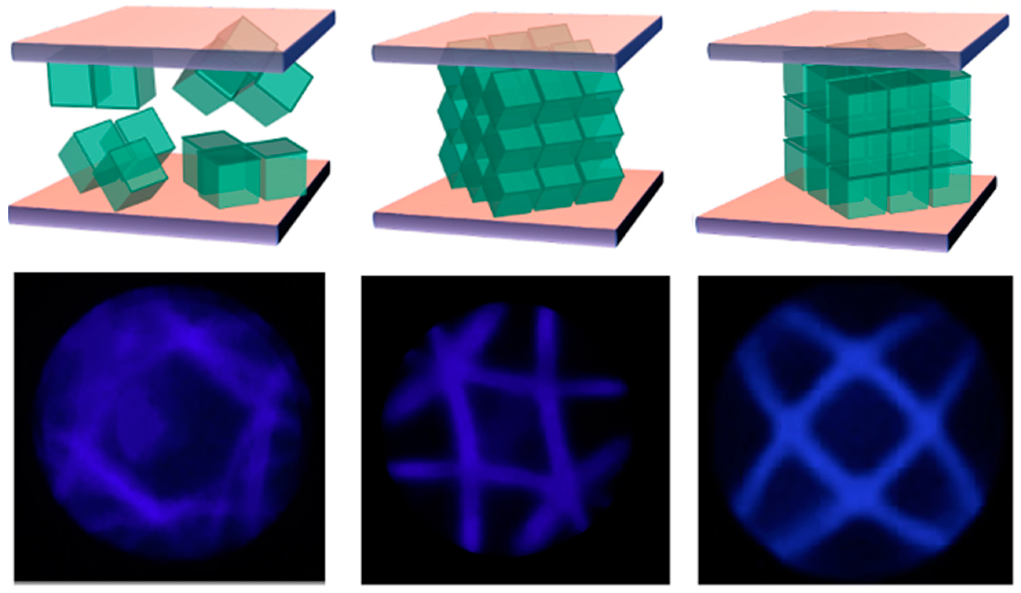
The Blue Phases of cholesteric liquid crystals have recently become a coveted approach for their potential in photonic applications because of their peculiar properties and structure. Blue Phases (BP) appear in chiral LCs that induce a high twisting of the director [69]. Contrary to other liquid crystal phases, BPs display a highly organized 3D structure with a lattice period in the hundreds of nanometers, which is achieved by the self-assembly of the LC molecules into periodic cubic structures that produce bright selective Bragg reflection in narrow bands.
BPs can be considered 3D photonic crystals as their sub-micrometer cubic structure is optically isotropic by symmetry. Unlike cholesteric liquid crystals, which only present Bragg reflection in one dimension, BPs are periodic in three dimensions. Therefore, they can produce multiple reflections in different directions [70,71]. Furthermore, their electro-optic behavior, with response times in the submillisecond range, additionally benefits their potential in photonics [72].
At different temperature ranges, three BP phases may appear—BPIII, BPII, and BPI from isotropic to cholesteric phases. The photonic crystal structures are found in BPI and BPII, which are self-assembled in an intricate double-twist cylinder structure that is organized in characteristic cubic lattices—body-centered (BCC) and simple cubic (SC), respectively [67].
3.1. Orientation of BPs
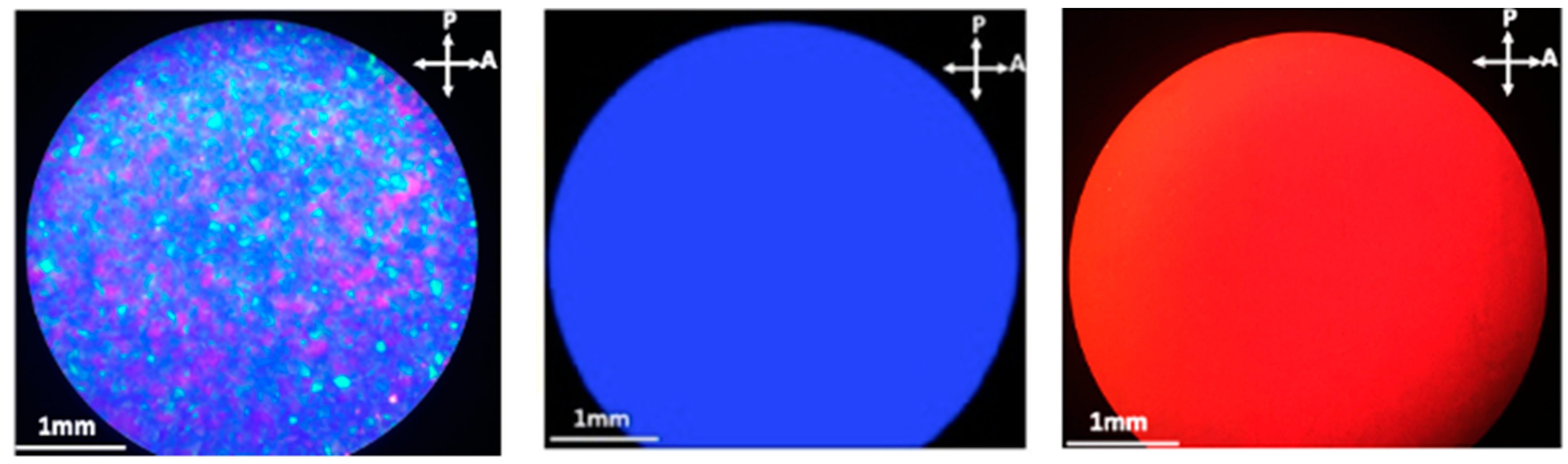
Optical devices based on BP liquid crystals usually require, as in other structures, a tightly controlled orientation of the material in the LC cell. Examples of BP crystals observed by polarizing optical microscopy are shown in Figure 14. Without any surface treatment, a typical polycrystalline structure (platelet structure) made of tiny, disorganized BP crystals is obtained (Figure 14, left). Platelet color is the result of the Bragg reflection from specific lattice planes.
Arranging the BP in the same lattice orientation with the same azimuthal angle is more complex than orienting nematics; still, it can be achieved. Figure 14 (center and right images) shows two BPs; the homogeneous texture and single-colored reflection suggest a single lattice orientation. However, standard manufacturing protocols often yield platelet BPs. Platelets produce high scattering, and their electro-optical response (when compared to monocrystalline BPs) is poorer [73].
Alignment control of BPs is an actual problem that needs to be successfully overcome to push the use of this advanced material in photonics. Their complex structure makes the lattice orientation control exceptionally challenging, and producing large BP monocrystals has been shown to be a particularly complex task.
3.1.1. Kossel Patterns
Monocrystallinity can be confirmed by Kossel pattern analysis. Kossel patterns are equivalent to Bragg’s X-ray diffraction patterns except that the wavelength is orders of magnitude longer, in the 100’s nm region, corresponding to the lattice period of the cubic structures adopted by BPs (actually, original Kossel is an X-ray divergent technique; the name has been kept for patterns in the visible range). Kossel patterns allow the identification of the BP phase (I or II), confirming the lattice orientation and its azimuthal angle and estimating the degree of monocrystallinity (blurry Kossel patterns suggest there is loss of monocrystallinity in the bulk because the resulting diffracted patterns are an average of the collective lattice orientation variations) [74].
Kossel patterns obtained for BP mono- and polycrystal are shown in Figure 15. Please note that the polycrystal structure produces a mix of numerous patterns overlapped with each other, while the monocrystals show a unique sharp pattern, confirming the single lattice orientation of the BP crystals—in this case, these are BPI (110) and BPI (200) (center and right images, respectively).
Controlling the growth of large BP crystals with a particular lattice plane orientation has just started to be explored. BPs can be produced as monocrystals with a unique lattice orientation by different methods.
3.1.2. Conventional Alignment
Conventional polyimide layers usually fail to produce aligned BP monocrystals, influenced by their strong anchoring energy, in the order of . The alignment can become extremely complex when taking into account the 3D orientation. Moreover, when BPI and BPII grow from different phases, they can show hysteresis. This suggests that the phase the BP is grown from can also impact the orientation [75].
Weak anchoring layers, like nylon (traditionally used for aligning for ferro- and antiferroelectric smectic liquid crystals), photoalignment, or soft-treated layers, can easily decrease anchoring energy by one or two orders of magnitude. Fixing a unique lattice orientation is, then, driven by the anchoring energy, where the interfacial free energy supports some lattice orientations and restricts others [76].
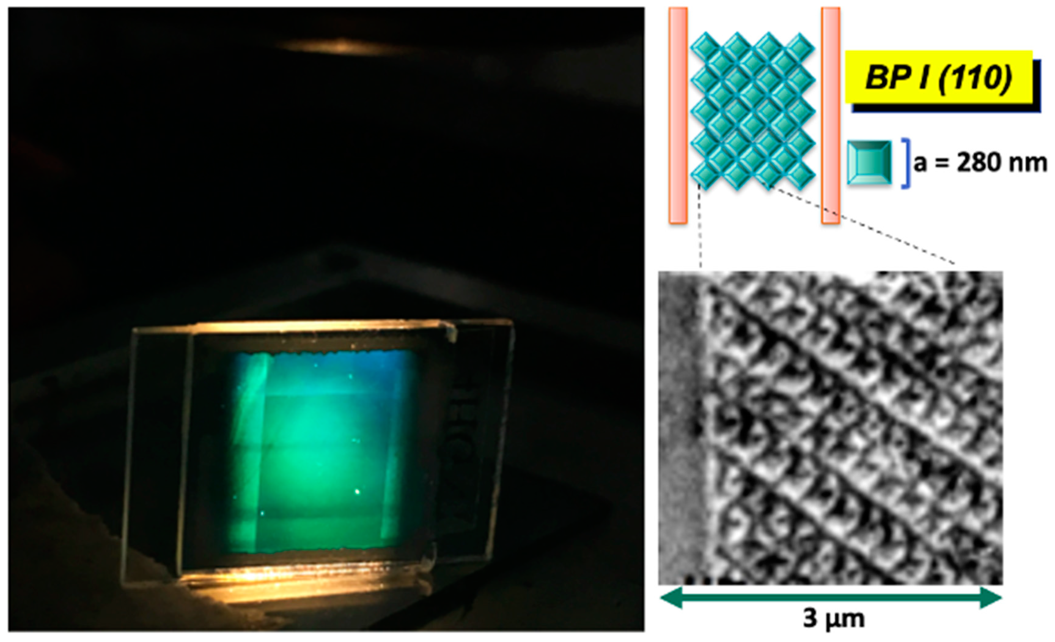
Surface treatments employing nylon-treated surfaces can produce BP monocrystals in large areas and stabilize them in temperature. By imposing precise confinement and anchoring, BPs of millimeter size with a uniform lattice orientation can be obtained.
3.1.3. Advanced Alignments
Moreover, by adjusting different BP precursor mixture formulations, it is possible to tailor the resulting lattice orientation of a BP crystal as desired when combined with smart surface treatments with weak anchoring energies. Having control of both lattice plane orientation and azimuthal orientation results in a unique orientation (Figure 16) of the 3D crystal. In addition, these methods allow the resolution of an unidentified lattice orientation of a given BP phase without the need for Kossel analysis [77].
Photoalignment-treated surfaces are another excellent candidate with weak anchoring energies, with the additional advantage of being able to be patterned by light with precise micro- or submicrometer-sized designs. A predefined pattern, recorded on a photoalignment-treated substrate, can induce the BP crystals to follow the pattern by exploiting field-induced phase transitions [78].
Large BP cells may show small localized crystalline defects not detected by Kossel analysis. In these cases, monocrystallinity can be demonstrated by direct observation of the bulk. This has been achieved in BPII by observing BP crystals by Transmission Electron Microscopy (TEM) and, most recently, in BPI (Figure 16, right) [79].
Other more sophisticated methods for orienting BPs rely on the design of nanopatterned surfaces. For instance, surfaces prepared by grafting polymer brushes or holographic lithography create nanopatterned gratings with periodic homeotropic and planar anchoring regions, which direct the lattice orientation of BPs [80,81].
3.2. Thermal Stabilization
A characteristic drawback of BPs is the extremely short temperature range where a particular phase can be found. Most BP formulations produce BPs that are intrinsically stable over small temperature ranges (usually a few degrees), and consequently, any reasonable application involving BPs will need a stabilization mechanism.
One of the most well-known methods of BP stabilization is polymer stabilization. A polymer-stabilized BP crystal is a mixture of the LC bearing the BP phase and a small amount of monomer. The mixture is thus mainly composed of a liquid crystalline material. During the polymerization process, the monomers added to the BP mixture are pushed out to the topological disclination lines of the BP cubic structure. Essentially, monomers polymerizing within the disclination lines function, in fact, as a scaffold supporting the whole structure [82].
Other stabilization methods rely on using an assortment of different kinds of doping materials inserted into the disclination lines, which aid in expanding the temperature ranges where the BP phases are present: using properly functionalized gold nanoparticles, highly stable BPs with adjustable optical properties can be obtained [83].
3.3. Applications of BPs
A quick look into previously reported research immediately reveals the wide variety of possible applications where Blue Phases might be involved, from color-changing films to lasing devices. Most devices proposed here can be fabricated with BPs, with the advantage of avoiding polarization dependence of the system. Moreover, several applications are specific to BPs.
By taking advantage of the everchanging Bragg reflection properties, it is possible to achieve stretchable BP gels [86] with flexible reflection peak or humidity-driven color-changing photonic polymer coatings [87].
Non-stabilized BPs, while working in the proper temperature ranges, or softly stabilized BP crystals can be addressed by electric fields, as well. In the electro-optics of BPs, there is a relationship between the amplitude of the applied field and the field-induced birefringence. By addressing BPs with electric fields, crystal lattices may deform to orthorhombic or tetragonal crystals by electrostriction [88,89].
BP electro-optic behavior can be described as in crystal optics by two components: a purely electro-optic effect, with refractive index modulation, and a secondary photo-elastic effect, with shifting of the Bragg reflection wavelength—they are both the result of molecular reorientation under applied fields.
The refractive index change is influenced by local reorientations of the nematic LC, and with very short pitches, the switching times become extremely short at submillisecond response times. The reflection wavelength shift, though, is the result of the deformation of the BP lattice to compensate for the increase of elastic energy with applied fields and is a much slower process.
In polymer-stabilized BP crystals, the lattice size is fixed and imposed by the polymeric network embedded into the crystal disclination lines. As a result, under applied fields, the secondary Bragg shift effect is suppressed, and there is only a fast refractive index modulation, which is ideal for phase modulation applications.
Different approaches to optical applications include polarization-independent phase modulation [71], where under applied voltage, well-aligned monocrystalline BPs generate higher phase shifts than platelet BPs.
Several Fresnel lenses based on BP LCs have been proposed [90]. Tunability can be controlled by adjusting the voltage applied to the edges of the Fresnel zones, while the aperture can be enlarged, increasing the number of zones of the lens.
In another interesting proposal, a Fresnel lens, made of a BP composite based on thermal-induced phase separation [91], and a BP microlens array, using progressive masks to produce the gradient distribution of the electric field, has been demonstrated [92].
By particular photo-patterning of BPII, a tunable polarization volume grating has been manufactured, which produces wide angles when compared with cholesteric LC-based gratings, owing to the high symmetry of its cubic structure [93].
Future BP devices for applications will probably be based on either polymer-stabilized (PS) or nanoparticle (NP)-doped BP LCs. Both show response times in the submillisecond range; the off-voltage state is isotropic, and manufacturing is relatively easy. However, the operating voltage is still high; PS BPs show noticeable hysteresis, and optical performance is low, while NP BPs’ temperature range is still narrow. The use of nanoparticle-doped PS BPs has been suggested [94]. Within certain limits, these materials show a wide temperature range, no hysteresis, and no residual birefringence.
There has been exceptional progress in new devices and applications for blue-phase photonic crystals in just the last few years. However, there are still many unknowns, especially in the alignment mechanism and targeting of the resulting orientation of the BP crystals. Controlling and understanding the underlying processes of alignment will be crucial to allow the development of this photonic material in any novel application.
4. Spirals
In recent years, geometric spirals have provided a powerful tool to develop several disruptive tunable circular optical devices with exceptional performance in terms of aperture, focal distance variability, and fill factor. Spirals are ideal for creating Fresnel structures with no connectivity issues, i.e., one of the most relevant obstacles for the fabrication of high-pixel-density Fresnel optical devices.
A full collection of tunable LC devices, including lenses, axicons, and spiral phase plates, have been developed. (Note: the shape of spiral phase plates or SPPs need not be spiral. The name comes from the fact that SPPs induce spiral wavefronts, according to their topological charge, on plane waves impinging on them. In our lab, twisted SPPs are used to obtain lenses or axicons, but SPPs without performing induce spiral wavefronts as well).
Before describing the actual devices, let us briefly review the most relevant spirals employed by our group in LC device design, as well as the main difficulties experienced in the fabrication of Fresnel elements.
4.1. Geometrical Spirals
A 2D spiral is a geometrical curve with a central origin that rotates about this origin while growing farther away. There are many examples in nature, from snail shells to galaxies.
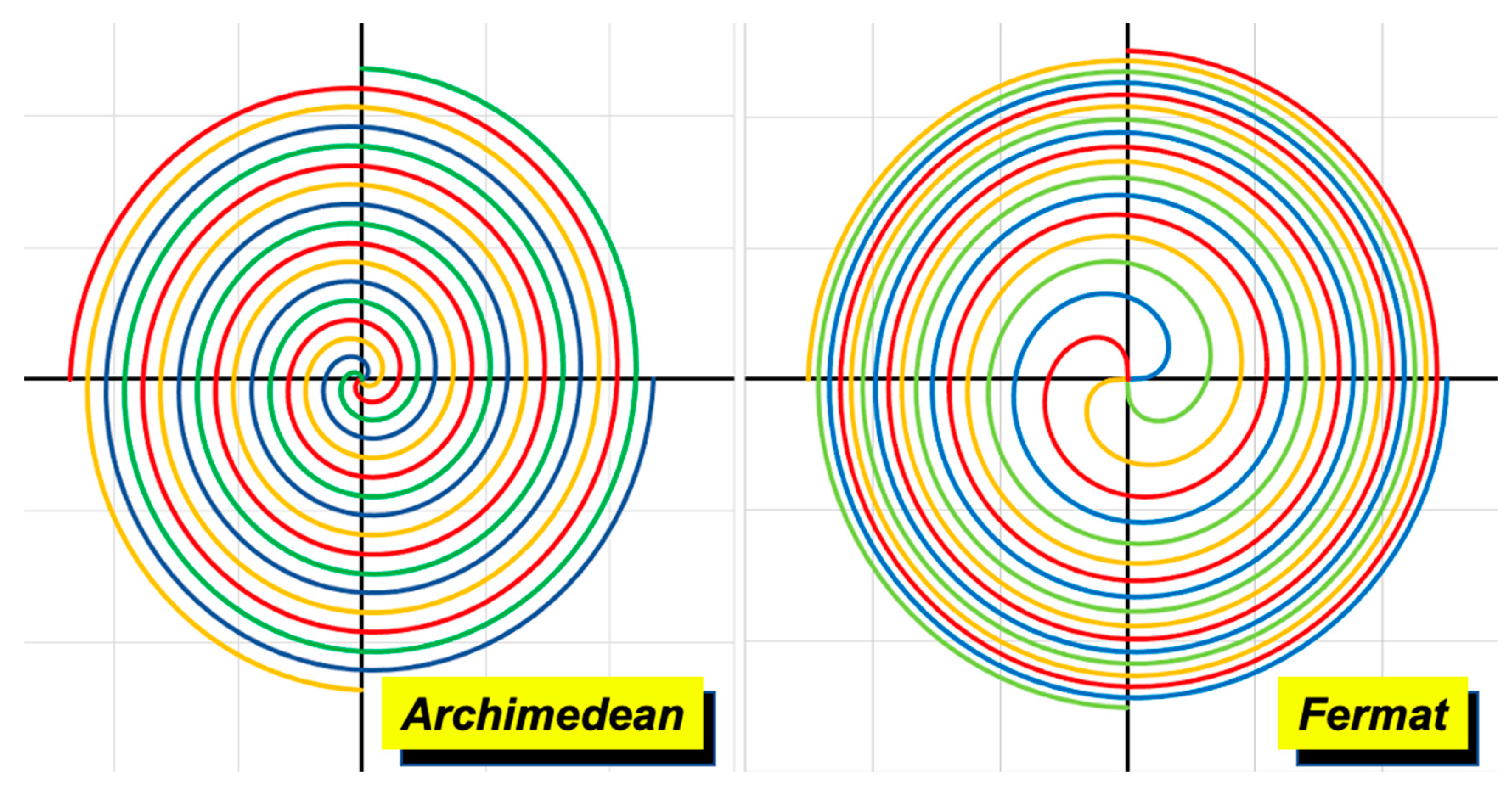
There is a high number of different 2D spirals—linear, quadratic, logarithmic, lituus, Fibonacci, Cornu, etc.—although the most interesting by now for optical design are two: the Archimedean or linear spiral and the Fermat or parabolic spiral (Figure 17). These two spirals, along with the lituus and the hyperbolic spiral, can be formulated [95] in polar coordinates with a general equation,
where is the radial distance, is the polar angle, is an arbitrary coefficient, and is a constant that measures the “tightness” of the spiral wrapping. Integer values define the abovementioned spirals: −2, −1, +1, +2 correspond to lituus, hyperbolic, Archimedean, and Fermat spirals, respectively.
The Archimedean spiral in polar coordinates is a simple increasing monotone function of radius with angle
that can be converted in coordinates using the trigonometrical relation.
The Fermat spiral is defined for as
The sign provides two branches of the spiral that meet at the center. Archimedean spirals, with their constant spacing, shall be used to design Fresnel axicons [96], whereas Fermat spirals provide an adequate shape for Fresnel lenses. Indeed, as shown in [97], the equation describing the constant phase spiral symmetry of the lens is
where are polar coordinates, is the lens focal distance, and is the topological charge. Within this frame, and considering phase wrapping, the Fermat spiral of Equation (13) becomes
In most applications, Equations (14) and (15) can be considered equivalent since usually
4.2. Experimental Implementations
Before proceeding any further, let us point out the main advantages of spiral designs for the implementation of actual circular optical LC devices.
4.2.1. Interleaving
Spirals can be easily interleaved with each other, as seen in Figure 17. The equation is the same; only a constant phase shift is required between consecutive curves.
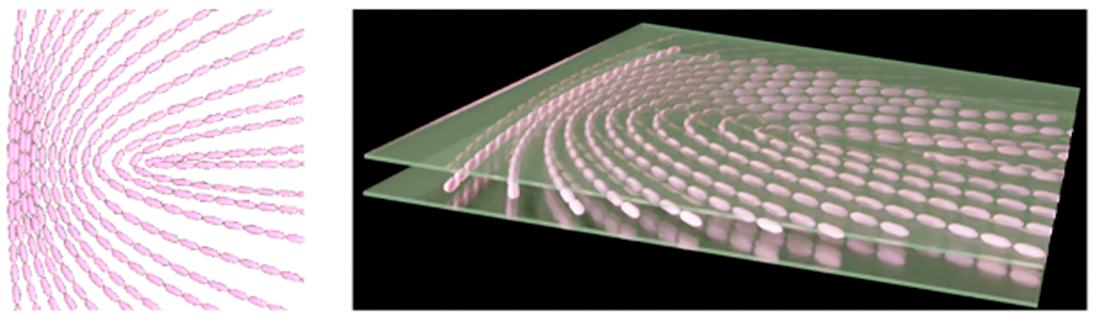
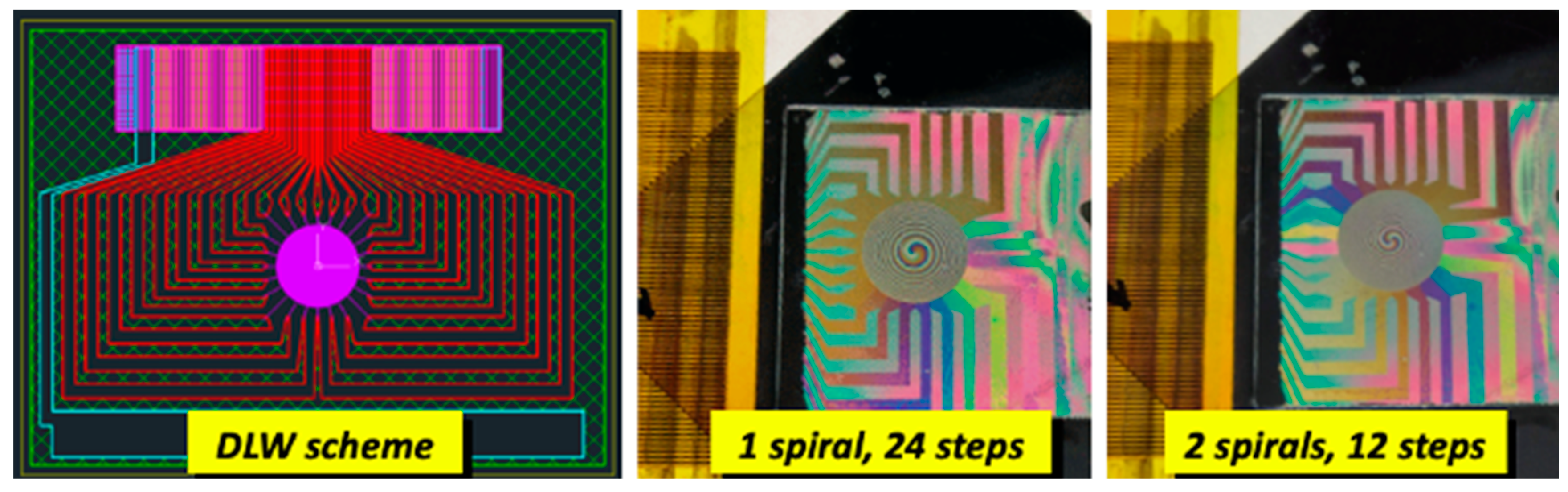
Consequently, spirals can be straightforwardly applied to design tracks for the device pixels. In our lab, spiral devices are fabricated with a non-photolithographic process based on Direct Laser Writing (DLW). A focused UV laser is used for ablation of the ITO coating of glass plates, thus delimiting the pixels with arbitrary forms (Figure 18).
Ablation creates trenches on the ITO, their gap width being 1–2 µm wide. If needed, the gap can be reduced to about 600 nm by employing a femtosecond IR laser working in dual photon mode. The area between two contiguous trenches (i.e., pixels) is continuous all along the curves, an issue that has crucial relevance in connections.
4.2.2. Electrical Connections
Interconnections with external drivers require electric continuity from the device’s edges to the center. Achieving this continuity is simple in modal lenses but becomes a significant hurdle in more complex designs such as Fresnel lenses, especially if the number of steps (pixels) of each tooth of the sawtooth is high.
Figure 19 illustrates a simplified example of connections required by a Fresnel lens made of 5 rings with 12 steps each. The upper part of the figure shows the outcome of the lens, where each color represents a different phase shift. In the bottom left, a sketch of the Fresnel lens made of concentric circles is shown. The radial lines show a scheme of electrical interconnections; since the inner electrodes must be isolated from the outer rings, a complex multilayer scheme must be considered. Please note that only the three internal rings have been sketched for simplicity.
As well as some elaborate electrode designs mentioned above [32,33,34], several authors have formulated various proposals to overcome this issue, such as variable transmission electrodes [98], interdigitated comb electrodes [99], microstructured transmission lines [100], or 4-electrode lenses with rectangular aperture [101]. Nevertheless, the electrode design is complex, and the control of the electric field distribution is limited in most cases.
4.3. Spirals as Alternative Approach
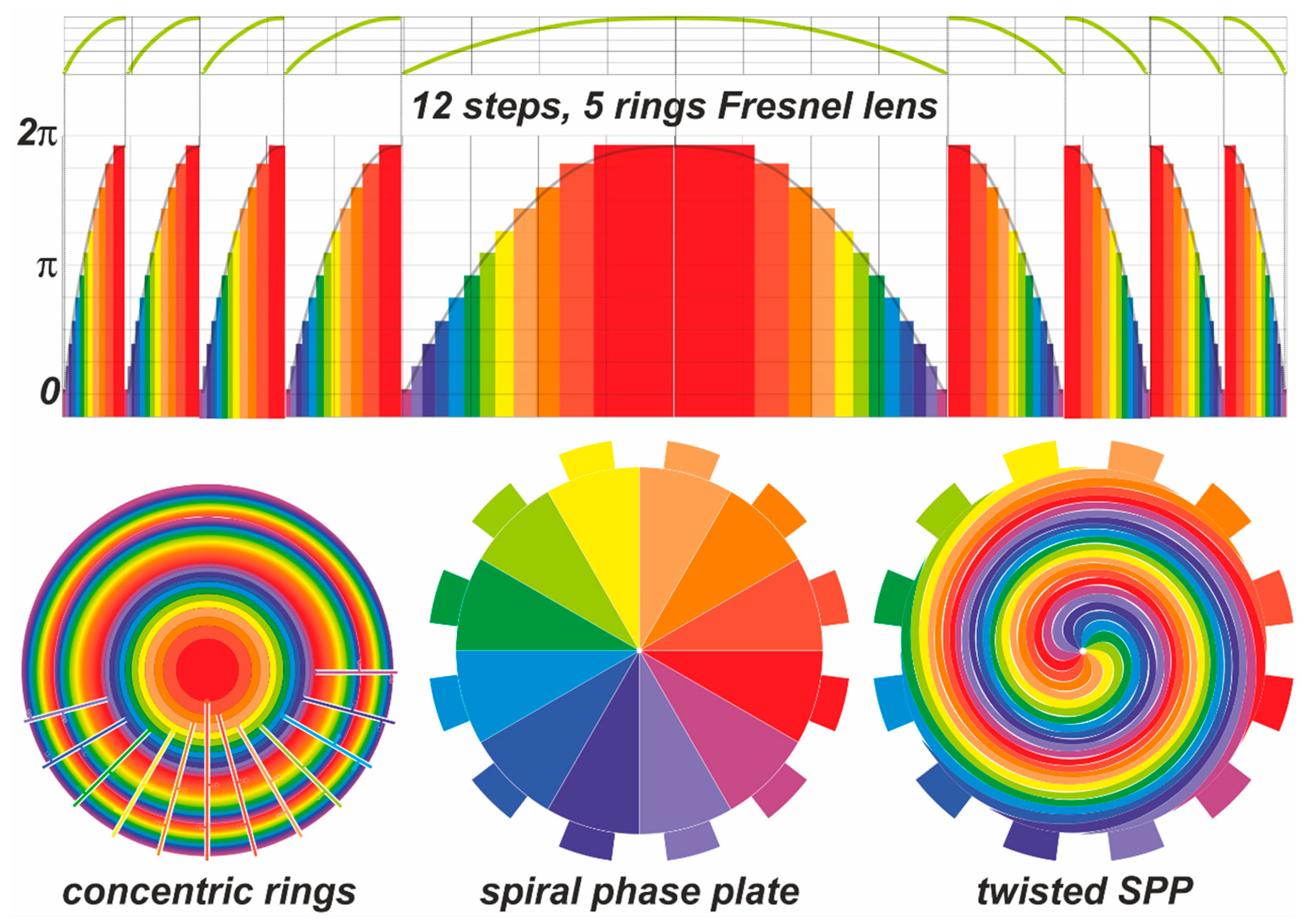
Electrical interconnections can be dramatically simplified using spirals rather than concentric circles in the preparation of the Fresnel lens. To create a 12-step, 5-ring Fresnel lens like that shown in Figure 19:
- Design a 12-pie slice spiral phase plate (Figure 19, bottom center) with external electric connections.
- Twist the SPP five turns.
4.3.1. Design of Spiral Lenses and Axicons
The 12 pie slices can be independently connected and will be used to arrange the steps of each Fresnel tooth. Electric continuity is guaranteed from the edge to the SPP center for each slice. The five turns will become the five teeth of the Fresnel lens. It could be argued that the tracks are not actually circles but spirals. However, increasing the number of turns, spirals, and circles become indistinguishable.
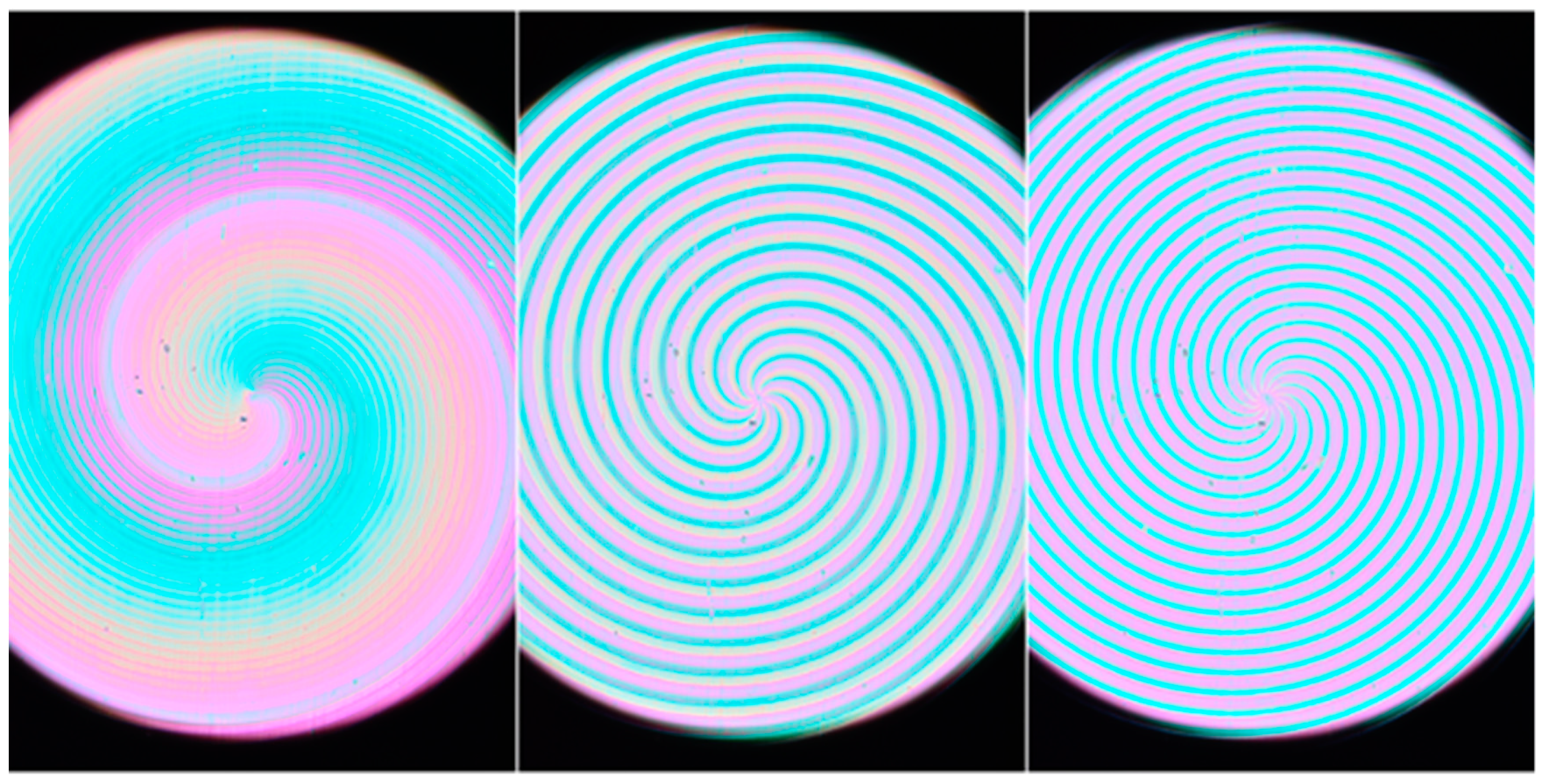
Figure 19, bottom right, shows a twisted SPP. It is just an example; it is not possible to visualize a five-turn spiral of these dimensions (spirals in the figure have less than 4π turns). Moreover, for the sake of clarity, an axicon rather than a lens (i.e., a set of Archimedean rather than Fermat spirals) is shown, like the example of Figure 20. The important point is to realize that the external connections keep electric continuity from the edge to the center; no further wiring is necessary.
An additional point is worth mentioning regarding Figure 20. The three photographs have been obtained with the same sample, a 24-pie slice SPP twisted about 3.5π. The teeth are made using all the slices as a single grayscale or gathering the slices in several groups. The rightmost picture with topological charge 12 is binary, i.e., the slices have either 0 or π phase shift alternatively, like the example shown in Figure 8.
4.3.2. Fill Factor
An additional advantage of the simple electrical connections of spirals is the fill factor, i.e., the fraction of the active area that is effectively used for developing the device, with no obstacles or dead zones. Active devices, like SLMs, usually feature poor fill factors (<40%) since the active components shadow the pixel area.
Passive devices with complex wiring often require multilayer arrangements and significant fractions of the working area are obstructed. On the other hand, spirals only contribute to shadowing areas with the interpixel DLW trenches (often blurred by fringing), which allows the fill factor to rise to very high values, about 98%.
4.4. Tunability of Spiral Lenses
4.4.1. Assembling Spiral Lenses
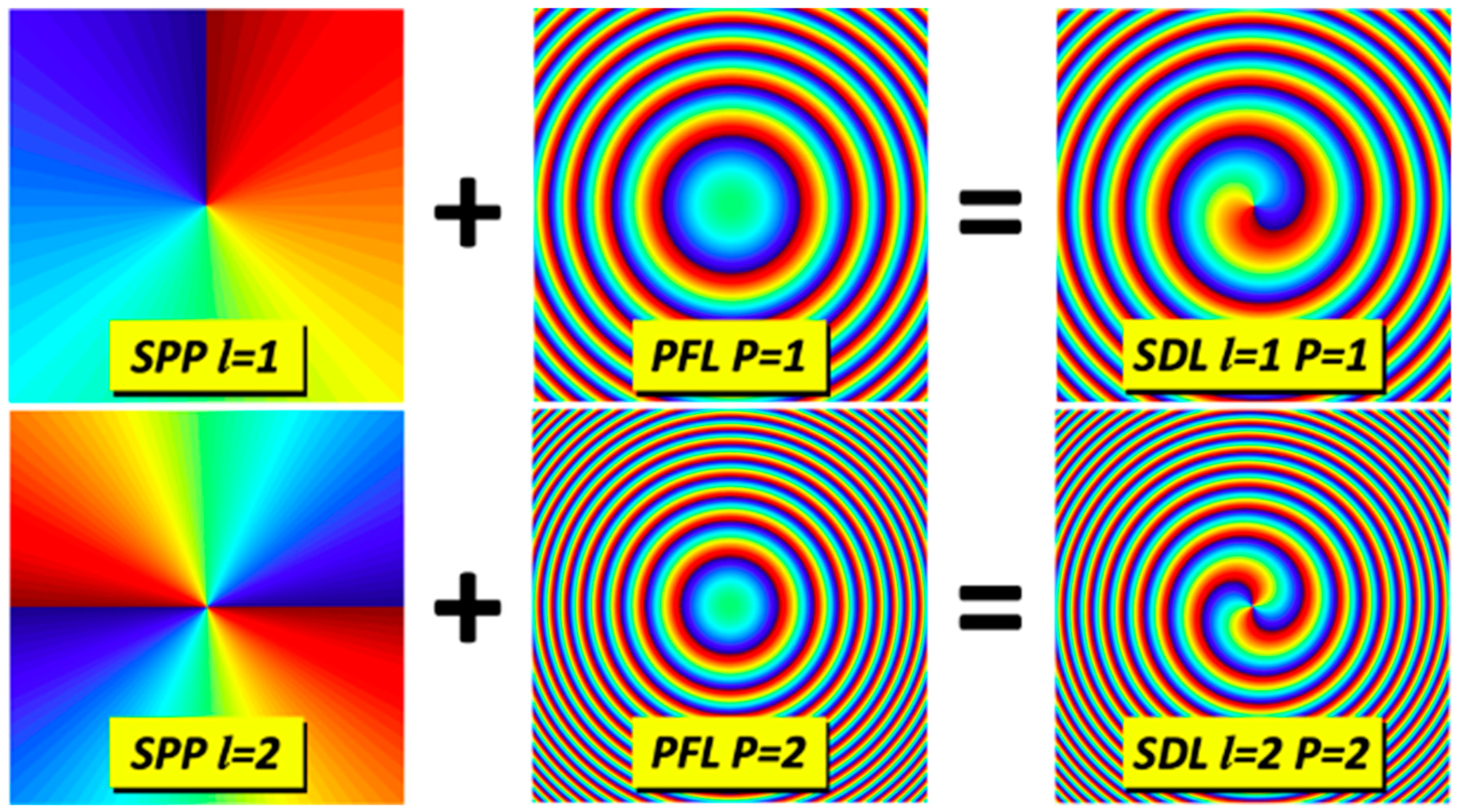
A spiral diffractive lens (SDL) is the result of combining an SPP with a certain number of slices and a Phase Fresnel Lens (PFL, to distinguish from intensity-driven Fresnel Zone Plates) with a certain number of rings and a given radius. Typically, the experimental SDLs created in our group have 24–72 (occasionally 144) pie slices and 14–40 turns (rings).
The outer (thinner) rings have thicknesses of a few µm; the lenses are somewhat in the limit between spiral diffractive lenses (SDL) and spiral refractive lenses (SRL), i.e., lenses derived from diffractive and refractive Fresnel lenses (DFL and RFL), respectively. DFLs are lenses in which diffractive phenomena are clearly present and affect the lens output, whereas these phenomena are negligible in RFLs. Using the name SDL rather than SRL is, therefore, arbitrary.
For a given set of pie slices and turns, different SDLs with different power and topological charges can be generated (Figure 21). The number of slices is usually chosen with many divisors, such as 24 or 72. For example, an SPP with 24 slices can support topological charges 1, 2, 3, 4, 6, 8, and 12, along with the corresponding negative values. Thus, 14 different lenses with different powers can be obtained.
4.4.2. Tunable SDLs
According to Equation (15),
A lens with a given radius and a certain number of turns , working at a given wavelength, may generate any lens with any power as long as the product is kept constant. That means that to double the power of the spiral lens, the topological charge must be doubled as well. Moreover, the topological charge can be positive or negative, therefore rendering convergent and divergent lenses with the same device.
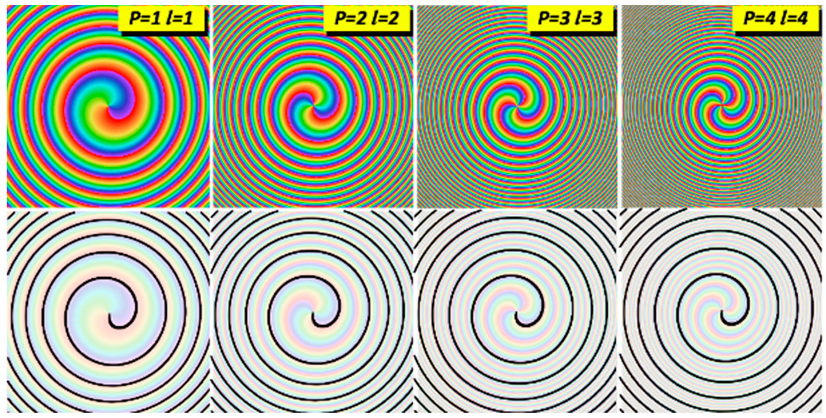
An example of a constant product is shown in Figure 22. The same device with a fixed number of turns, as defined by the black spiral shown in the bottom row, can provide different powers increasing the topological charge . Please note that the spiral overlaps all the configurations. Negative topological charges will show an opposite color sequence (i.e., phase sequence).
This rule only applies if one wants to obtain different configurations of the same device. There is no problem in combining, e.g., an SPP with with a PFL with (after all, the lens powers are arbitrary), but a different device must be used.
4.4.3. Analog vs. Digital SDLs
Anyhow, it seems that only specific values of topological charges, hence lens powers, can be obtained in a given lens. Nevertheless, if the number of slices is increased sufficiently, the difference between achieved powers can be very low. Thus, an SDR with 72 slices of 2 diopters offers 11 power levels; the difference between them is relatively large for high values (2, 1.5, 1 … diopters) but becomes very small (1/36th diopter) for the low end.
Any topological charge up to half the number of slices can be obtained. The charge need not be a divisor of the slice number. However, to obtain a topological charge, e.g., , the slice groups would not run from , but to scattered values that would probably work against the optical quality of the lens.
4.4.4. Obtaining True Fresnel Lenses
A serious drawback of spiral diffractive lenses is the intrinsic presence of an optical vortex in the structure. The optical vortex by itself generates a pattern with a black dot in the center, where all phases cancel out.
Therefore, the lenses based on spirals do not produce correct images since the image center is blackened by the vortex. Fortunately, there are several procedures to overcome this inconvenience, all based on “unwinding” the spiral [104]:
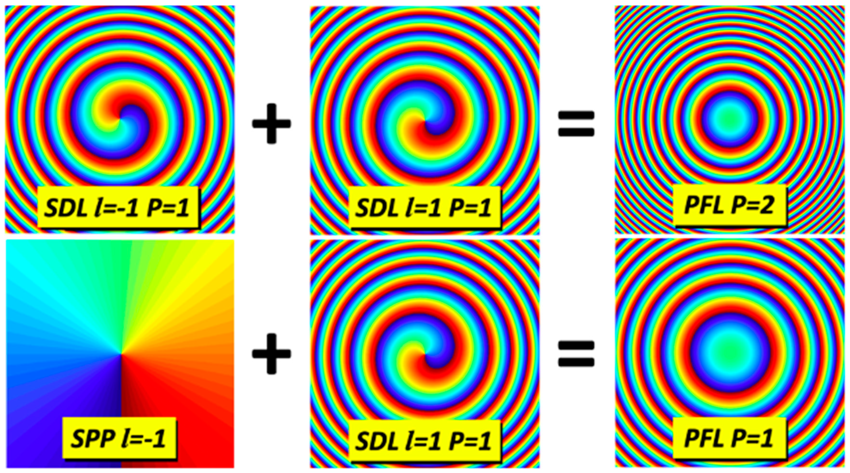
- By superimposing on the SDL an SPP with the same topological charge but opposite sign, the topological charges cancel out, and the result is equivalent to a classical Fresnel lens of the same power.
- The topological charge can also be canceled by using two identical lenses with an inverse topological charge. It is achieved by building a device made up of two units of the same lens coupled back-to-back. The topological cancelation is identical to the previous case, but the power of the resulting lens is twice the power of the individual lenses.
The two cases are summarized in Figure 23. In the upper part, two identical lenses are coupled back-to-back to cancel out the topological charge; the obtained PFL has a power twice the power of a single lens. In the lower part, the topological charge of the SDL is compensated with an SPP of the same topological charge but with an opposite sign. In this case, the topological charge is canceled, but the power of the PFL is the same as the power of a single lens.
4.4.5. Experimental Verification
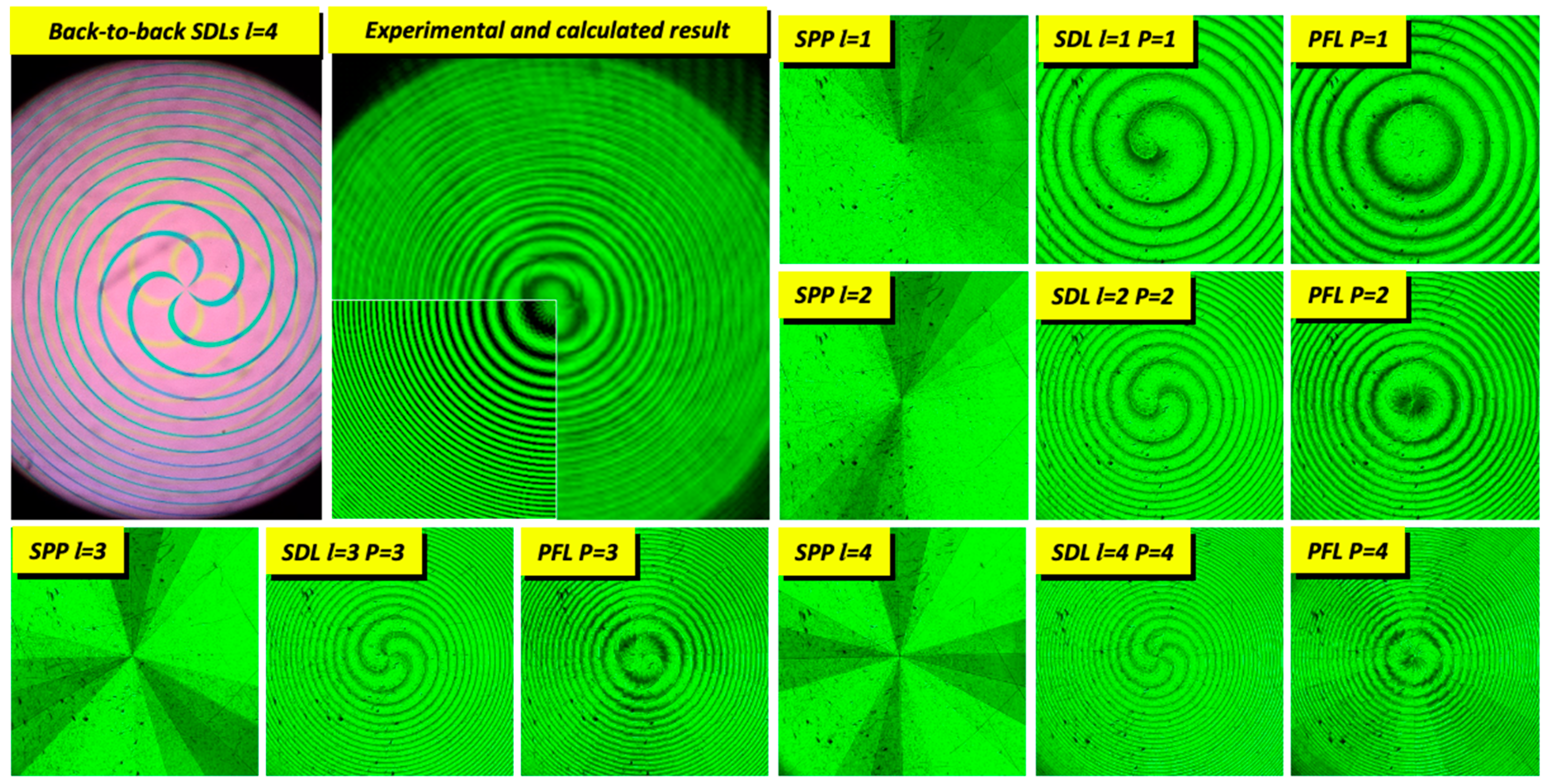
Although the mathematical calculations shown above indicate that perfect Fresnel lenses can be obtained, it is necessary to verify the results because, under actual experimental conditions, deviations from the theoretical results may arise due to spurious reflections at the interfaces, liquid crystal misalignments, and sample imperfections.
Some experimental results obtained with spiral lenses and spiral phase plates are shown in Figure 24. In the upper left figure, two identical SDLs are placed back-to-back. In the figure, one of the spirals on each SDL is arbitrarily excited so that the opposite rotation of both SDLs can be appreciated.
The remaining sets of pictures are SDLs and SPPs of different topological charges combined to cancel out the topological charge in the resulting Fresnel lens. The experimental images provide a good match with the expected Fresnel lenses. Above all, no residuals of vortices have been found. Nevertheless, some deviations of actual images from expected results are appreciated.
It has been found that perfect alignment of the elements is critical so that the resulting Fresnel lens does not appear distorted. Most defects found in the assembled system are attributed to micrometric deviations of elements. The defects increase with the topological charge since smaller features are involved in the resulting images.
The use of index-matching gels to reduce spurious reflections has produced no apparently improved samples. Possibly, this kind of procedure would be advantageous in industrial production, but it significantly increases the process complexity without decisive advantages.
5. Conclusions
Phase-only circular liquid crystal devices can provide several useful tunable tools for different applications. The devices can be used individually or combined in more complex systems, widening their applicability. In this work, several LC devices have been analyzed—axicons, spiral phase plates, vortices, and lenses. Direct laser writing stands out as a powerful technique for the flexible design of such devices.
External driving requiring complex connections can be greatly simplified by employing spirals. Spirals mimic Fresnel diffractive and refractive lenses and axicons. Quasi-analog tunability can be achieved by increasing the number of steps defining each Fresnel ring.
Residual vortices generated by the twisted structure can be canceled out using pairs of back-to-back lenses/axicons or compensating phase plates. Overall, a full family of circular tunable LC devices with limitless applications can be created from basic Archimedean and Fermat spirals.
Author Contributions
Conceptualitation, J.M.O., X.Q. and M.C.-G.; methodology E.O., M.C.-G. and J.P.-G.; software M.A.G. and J.P.-G.; validation, all; formal analysis, J.M.O., X.Q. and E.O.; investigation, all; resources, J.P.-G., M.C.-G. and M.A.G.; writing, all; original draft preparation, J.M.O. and E.O.; review and editing, all; supervision, J.M.O. All authors have read and agreed to the published version of the manuscript.
Funding
This research was funded by the Comunidad de Madrid through the “Programa de Actividades de I + D” (“SINFOTON2-CM”—S2018/NMT-4326), “PANTOMIME” APOYO-JOVENES-21-9FOMOQ-22-0CNGFM, “DISEÑO Y FABRICACIÓN DE DISPOSITIVOS FOTÓNICOS” (BEAGALINDO-21-QU81R4-7-0QQBF3) and the “Ayudas para la realización de Doctorados Industriales de la Comunidad de Madrid” (IND2020/TIC-17424). The financial support to this study has also come from the Spanish Government, “ENHANCE-5G” (PID2020-114172RB-C22), “LC-LENS” (PDC2021-121370-C21), “DISRADIO” (TSI-063000-2021-83) and WOW-2D (PLEC2022-009381), as well as the Attract-IALL EU project G.A 101004462, financed by the European Union. In addition, authors are grateful to the European Space Agency (ESA) for the financial support received with the “Smart Heaters” project (4000133048/20/NL/KML). MCG is grateful to Spanish government grant (BG20/00136).
Data Availability Statement
This is a review work. All data are contained within the article.
Conflicts of Interest
The authors declare no conflicts of interest.
References
- Singh, A. Liquid Crystal Spatial Light Modulators. Available online: https://www.slideshare.net/azadajay/liquid-crystal-slms (accessed on 13 May 2023).
- Pinho, C.; Alimi, I.; Lima, M.; Monteiro, P.; Teixeira, A. Spatial Light Modulation as a Flexible Platform for Optical Systems. In Telecommunications Systems—Principles and Applications of Wireless-Optical Technologies; Alimi, I.A., Monteiro, P.P., Teixeira, A.L., Eds.; IntechOpen: Rijeka, Croatia, 2021; ISBN 978-1-78984-294-4. [Google Scholar] [CrossRef]
- Drăgulinescu, A. Optical Correlators for Cryptosystems and Image Recognition: A Review. Sensors 2023, 23, 907. [Google Scholar] [CrossRef] [PubMed]
- Chou, H.-H.; Chen, C.-L. Asymmetric Optical Wavelength Switch Based on LCoS-SLM for Edge Node of Optical Access Network. IEEE Photon-J. 2021, 13, 1. [Google Scholar] [CrossRef]
- Ma, Y.; Stewart, L.; Armstrong, J.; Clarke, I.G.; Baxter, G.W. Recent Progress of Wavelength Selective Switch. J. Light. Technol. 2021, 39, 896. [Google Scholar] [CrossRef]
- Lee, B.; Kim, D.; Lee, S.; Chen, C. High-contrast, speckle-free, true 3D holography via binary CGH optimization. Sci. Rep. 2022, 12, 2811. [Google Scholar] [CrossRef] [PubMed]
- Lingel, C.; Haist, T.; Osten, W. Spatial-light-modulator-based adaptive optical system for the use of multiple phase retrieval methods. Appl. Opt. 2016, 55, 10329. [Google Scholar] [CrossRef] [PubMed]
- Wu, Q.; Sui, X.; Fei, Y.; Xu, C.; Liu, J.; Gu, G.; Chen, Q. Multi-layer optical Fourier neural network based on the convolution theorem. AIP Adv. 2021, 11, 055012. [Google Scholar] [CrossRef]
- Dean, J. How Spatial Light Modulators Speed Optical Computing Applications. 2018. Available online: https://www.playbuzz.com/podrobnostiua10/10-20-2016-11-22-25-am10 (accessed on 13 June 2023).
- Wu, J.; Lin, X.; Guo, Y.; Liu, J.; Fang, L.; Jiao, S.; Dai, Q. Analog Optical Computing for Artificial Intelligence. Engineering 2022, 10, 133. [Google Scholar] [CrossRef]
- Davis, J.A.; Hall, T.I.; Moreno, I.; Sorger, J.P.; Cottrell, D.M. Programmable Zoom Lens System with Two Spatial Light Modulators: Limits Imposed by the Spatial Resolution. Appl. Sci. 2018, 8, 1006. [Google Scholar] [CrossRef]
- Caputo, R.; De Luca, A.; Strangi, G.; Bartolino, R.; Umeton, C.; De Sio, L.; Veltri, A.; Serak, S.; Tabiryan, N. The POLICRYPS liquid-crystalline structure for optical applications. Adv. Opt. Technol. 2018, 7, 273. [Google Scholar] [CrossRef]
- de Blas, M.G.; García, J.P.; Andreu, S.V.; Arregui, X.Q.; Caño-García, M.; Geday, M.A. High resolution 2D beam steerer made from cascaded 1D liquid crystal phase gratings. Sci. Rep. 2022, 12, 5145. [Google Scholar] [CrossRef]
- Paschotta, R. Axicons. RP Photonics Encyclopedia. Available online: https://www.rp-photonics.com/axicons.html (accessed on 8 June 2023). [CrossRef]
- Lee, D.; Lee, H.; Migara, L.K.; Kwak, K.; Panov, V.P.; Song, J. Widely Tunable Optical Vortex Array Generator Based on Grid Patterned Liquid Crystal Cell. Adv. Opt. Mater. 2021, 9, 2001604. [Google Scholar] [CrossRef]
- Gomez, M.A.; Snow, J.C. How to construct liquid-crystal spectacles to control vision of real-world objects and environments. Behav. Res. Methods 2023, 2. [Google Scholar] [CrossRef] [PubMed]
- Bailey, J.; Morgan, P.B.; Gleeson, H.F.; Jones, J.C. Switchable Liquid Crystal Contact Lenses for the Correction of Presbyopia. Crystals 2018, 8, 29. [Google Scholar] [CrossRef]
- Lee, S.; Park, G.; Kim, S.; Ryu, Y.; Yoon, J.W.; Hwang, H.S.; Song, I.S.; Lee, C.S.; Song, S.H. Geometric-phase intraocular lenses with multifocality. Light. Sci. Appl. 2022, 11, 320. [Google Scholar] [CrossRef] [PubMed]
- Zhang, X.; Cao, Z.; Mu, Q.; Li, D.; Peng, Z.; Yang, C.; Liu, Y.; Xuan, L. Progress of liquid crystal adaptive optics for applications in ground-based telescopes. Mon. Not. R. Astron. Soc. 2020, 494, 3536. [Google Scholar] [CrossRef]
- Wang, J.; Jákli, A.; Guan, Y.; Fu, S.; West, J. Developing Liquid-Crystal Functionalized Fabrics for Wearable Sensors. Inf. Disp. 2017, 33, 16. [Google Scholar] [CrossRef]
- Kawamura, M. Tunable Liquid Crystal Lenses and Their Applications. J. Photopolym. Sci. Technol. 2019, 32, 559. [Google Scholar] [CrossRef]
- Galstian, T.; Sova, O.; Asatryan, K.; Presniakov, V.; Zohrabyan, A.; Evensen, M. Optical camera with liquid crystal autofocus lens. Opt. Express 2017, 25, 29945. [Google Scholar] [CrossRef]
- Tian, J.-Q.; Zhao, Z.-Z.; Li, L. Adaptive liquid lens with a tunable field of view. Opt. Express 2022, 30, 40991. [Google Scholar] [CrossRef]
- Huang, H.; Zhao, Y. Optofluidic lenses for 2D and 3D imaging. J. Micromech. Microeng. 2019, 29, 073001. [Google Scholar] [CrossRef]
- Schneider, J. The First Smartphone to Use a Liquid Lens is the Xiaomi Mi Mix Fold. Petapixel March. 2021. Available online: https://petapixel.com/2021/03/30/the-first-smartphone-to-use-a-liquid-lens-is-the-xiaomi-mi-mix-fold/ (accessed on 18 June 2023).
- LibreTexts Physics. Geometric Optics: Lenses. Available online: https://phys.libretexts.org/Bookshelves/University_Physics/Book%3A_Physics_(Boundless)/24%3A_Geometric_Optics/24.3%3A_Lenses (accessed on 18 June 2023).
- Beeckman, J.; Yang, T.-H.; Nys, I.; George, J.P.; Lin, T.-H.; Neyts, K. Multi-electrode tunable liquid crystal lenses with one lithography step. Opt. Lett. 2018, 43, 271. [Google Scholar] [CrossRef] [PubMed]
- Ahmadalidokht, I.; Mohajerani, E.; Mohammadimasoudi, M. Fabrication and characterization of large aperture adaptive modal liquid crystal lens with a PEDOT:PSS/PVA/DMSO blend used as the modal and rubbing layer. Opt. Mater. Express 2021, 11, 1259. [Google Scholar] [CrossRef]
- Huang, C.-Y.; Hsu, C.J.; Agrahari, K.; Selvaraj, P.; Chiang, W.F.; Huang, C.Y.; Manohar, R. Modal liquid crystal lens fabricated with ultra-thin ITO film. SPIE Proc. 2020, 11303, 1130303. [Google Scholar] [CrossRef]
- Algorri, J.F.; Zografopoulos, D.C.; Rodríguez-Cobo, L.; Sánchez-Pena, J.M.; López-Higuera, J.M. Engineering Aspheric Liquid Crystal Lenses by Using the Transmission Electrode Technique. Crystals 2020, 10, 835. [Google Scholar] [CrossRef]
- Sova, O.; Galstian, T. Modal control refractive Fresnel lens with uniform liquid crystal layer. Opt. Commun. 2020, 474, 126056. [Google Scholar] [CrossRef]
- Stevens, J.; Galstian, T. Electrically tunable liquid crystal lens with a serpentine electrode design. Opt. Lett. 2022, 47, 910. [Google Scholar] [CrossRef] [PubMed]
- Pusenkova, A.; Sova, O.; Galstian, T. Electrically variable liquid crystal lens with spiral electrode. Opt. Commun. 2021, 508, 127783. [Google Scholar] [CrossRef]
- Feng, W.; Ye, M. Positive-Negative Tunable Liquid Crystal Lens of Rectangular Aperture. IEEE Photon- Technol. Lett. 2022, 34, 795. [Google Scholar] [CrossRef]
- Perera, K.; Nemati, A.; Mann, E.K.; Hegmann, T.; Jákli, A. Converging Microlens Array Using Nematic Liquid Crystals Doped with Chiral Nanoparticles. ACS Appl. Mater. Interfaces 2021, 13, 4574. [Google Scholar] [CrossRef]
- Lee, Y.-H.; Tan, G.; Zhan, T.; Weng, Y.; Liu, G.; Gou, F.; Peng, F.; Tabiryan, N.V.; Gauza, S.; Wu, S.-T. Recent progress in Pancharatnam–Berry phase optical elements and the applications for virtual/augmented realities. Opt. Data Process. Storage 2017, 3, 79. [Google Scholar] [CrossRef]
- Fu, W.; Zhou, Y.; Yuan, Y.; Lin, T.; Zhou, Y.; Huang, H.; Fan, F.; Wen, S. Generalization of Pancharatnam-Berry phase interference theory for fabricating phase-integrated liquid crystal optical elements. Liq. Cryst. 2020, 47, 369. [Google Scholar] [CrossRef]
- Yousefzadeh, C.; Jamali, A.; McGinty, C.; Bos, P.J. “Achromatic limits” of Pancharatnam phase lenses. Appl. Opt. 2018, 57, 1151–1158. [Google Scholar] [CrossRef] [PubMed]
- Senyuk, B. Liquid Crystals: A Simple View on a Complex Matter. Available online: http://personal.kent.edu/~bisenyuk/liquidcrystals/maintypes3.html (accessed on 23 June 2023).
- Lin, Y.-H.; Wang, Y.-J.; Reshetnyak, V. Liquid crystal lenses with tunable focal length. Liq. Cryst. Rev. 2017, 5, 111. [Google Scholar] [CrossRef]
- Algorri, J.F.; Zografopoulos, D.C.; Urruchi, V.; Sánchez-Pena, J.M. Recent Advances in Adaptive Liquid Crystal Lenses. Crystals 2019, 9, 272. [Google Scholar] [CrossRef]
- Bennis, N.; Jankowski, T.; Strzezysz, O.; Pakuła, A.; Zografopoulos, D.C.; Perkowski, P.; Sánchez-Pena, J.M.; López-Higuera, J.M.; Algorri, J.F. A high birefringence liquid crystal for lenses with large aperture. Sci. Rep. 2022, 12, 14603. [Google Scholar] [CrossRef] [PubMed]
- Iwase, T.; Onaka, J.; Emoto, A.; Koyama, D.; Matsukawa, M. Relationship between liquid crystal layer thickness and variable-focusing characteristics of an ultrasound liquid crystal lens. Jpn. J. Appl. Phys. 2022, 61, SG1013. [Google Scholar] [CrossRef]
- Wang, X.-Q.; Yang, W.-Q.; Liu, Z.; Duan, W.; Hu, W.; Zheng, Z.-G.; Shen, D.; Chigrinov, V.G.; Kwok, H.-S. Switchable Fresnel lens based on hybrid photo-aligned dual frequency nematic liquid crystal. Opt. Mater. Express 2016, 7, 8. [Google Scholar] [CrossRef]
- Hsu, C.J.; Selvaraj, P.; Huang, C.Y. Low-voltage tunable liquid crystal lens fabricated with self-assembled polymer gravel arrays. Opt. Express 2020, 28, 6582. [Google Scholar] [CrossRef]
- Li, R.; Chu, F.; Tian, L.-L.; Gu, X.-Q.; Zhou, X.-Y.; Wang, Q.-H. Liquid crystal lenticular lens array with extended aperture by using gradient refractive index compensation. Liq. Cryst. 2020, 48, 378. [Google Scholar] [CrossRef]
- Algorri, J.F.; Bennis, N.; Urruchi, V.; Morawiak, P.; Sánchez-Pena, J.M.; Jaroszewicz, L.R. Tunable liquid crystal multifocal microlens array. Sci. Rep. 2017, 7, 17318. [Google Scholar] [CrossRef]
- Jamali, A.; Bryant, D.; Zhang, Y.; Grunnet-Jepsen, A.; Bhowmik, A.; Bos, P.J. Design of Large Aperture Tunable Refractive Fresnel Liquid Crystal Lens. Appl. Opt. 2017, 57, B10–B19. [Google Scholar] [CrossRef] [PubMed]
- Khonina, S.N.; Kazanskiy, N.L.; Khorin, P.A.; Butt, M.A. Modern Types of Axicons: New Functions and Applications. Sensors 2021, 21, 6690. [Google Scholar] [CrossRef] [PubMed]
- Khonina, S.N.; Kazanskiy, N.L.; Karpeev, S.V.; Butt, M.A. Bessel beam: Significance and applications—A progressive review. Micromachines 2020, 11, 997. [Google Scholar] [CrossRef]
- Khonina, S.N.; Ustinov, A.V.; Kharitonov, S.I.; Fomchenkov, S.A.; Porfirev, A.P. Optical Bottle Shaping Using Axicons with Amplitude or Phase Apodization. Photonics 2023, 10, 200. [Google Scholar] [CrossRef]
- Kim, J.A.; Lee, K.I.; Noh, H.R.; Jhe, W.; Ohtsu, M. Atom Trap in an Axicon Mirror. Opt. Lett. 1997, 22, 117. [Google Scholar] [CrossRef] [PubMed]
- Blank, V.A.; Strelkov, Y.S.; Skidanov, R.V. Axicon for imaging spectrometer. J. Phys. Conf. Ser. 2019, 1368, 022003. [Google Scholar] [CrossRef]
- Doshay, S.; Sell, D.; Yang, J.; Yang, R.; Fan, J.A. High-performance axicon lenses based on high-contrast, multilayer gratings. APL Photon. 2018, 3, 011302. [Google Scholar] [CrossRef]
- Pereiro-García, J.; García-De-Blas, M.; Geday, M.A.; Quintana, X.; Caño-García, M. Flat variable liquid crystal diffractive spiral axicon enabling perfect vortex beams generation. Sci. Rep. 2023, 13, 2385. [Google Scholar] [CrossRef]
- Shen, Y.; Wang, X.; Xie, Z.; Min, C.; Fu, X.; Liu, Q.; Gong, M.; Yuan, X. Optical vortices 30 years on: OAM manipulation from topological charge to multiple singularities. Light. Sci. Appl. 2019, 8, 90. [Google Scholar] [CrossRef]
- Aleksanyan, A.; Kravets, N.; Brasselet, E. Multiple-star system adaptive vortex coronagraphy using a liquid crystal light valve. Phys. Rev. Lett. 2017, 118, 203902. [Google Scholar] [CrossRef]
- Piccirillo, B.; Piedipalumbo, E.; Marruccia, L.; Santamato, E. Electrically tunable vector vortex coronagraphs based on liquid-crystal geometric phase waveplates. Mol. Cryst. Liq. Cryst. 2019, 684, 15–23. [Google Scholar] [CrossRef]
- Petrov, N.V.; Sokolenko, B.; Kulya, M.S.; Gorodetsky, A.; Chernykh, A.V. Design of broadband terahertz vector and vortex beams: I. Review of materials and components. Light. Adv. Manuf. 2022, 3, 640. [Google Scholar] [CrossRef]
- Deachapunya, S.; Srisuphaphon, S.; Buathong, S. Production of orbital angular momentum states of optical vortex beams using a vortex half-wave retarder with double-pass configuration. Sci. Rep. 2022, 12, 6061. [Google Scholar] [CrossRef]
- Schmiegelow, C.T.; Schulz, J.; Kaufmann, H.; Ruster, T.; Poschinger, U.G.; Schmidt-Kaler, F. Transfer of optical orbital angular momentum to a bound electron. Nat. Commun. 2016, 7, 12998. [Google Scholar] [CrossRef]
- Willner, A.E.; Song, H.; Zou, K.; Zhou, H.; Su, X. Orbital Angular Momentum Beams for High-Capacity Communications. J. Light. Technol. 2022, 41, 1918. [Google Scholar] [CrossRef]
- Zang, X.; Singh, N.; Lusk, M.T.; Schwingenschlögl, U. Conversion of twisted light to twisted excitons using carbon nanotubes. NPJ Comput. Mater. 2023, 8, 42. [Google Scholar] [CrossRef]
- Liu, Y.; Ke, Y.; Zhou, J.; Liu, Y.; Luo, H.; Wen, S.; Fan, D. Generation of perfect vortex and vector beams based on Pancharatnam-Berry phase elements. Sci. Rep. 2017, 7, 44096. [Google Scholar] [CrossRef]
- Geday, M.A.; Quintana, X.; Pereiro-García, J.; de la Rosa, P.; Otón, J.M.; Caño-García, M. Light with a twist. In Proceedings of the 16th European Conference on Liquid Crystals ECLC’23, Rende, Italy, 10–14 July 2023. [Google Scholar]
- Zhan, T.; Lee, Y.-H.; Tan, G.; Xiong, J.; Yin, K.; Gou, F.; Zou, J.; Zhang, N.; Zhao, D.; Yang, J.; et al. Pancharatnam–Berry optical elements for head-up and near-eye displays [Invited]. J. Opt. Soc. Am. B 2019, 36, D52. [Google Scholar] [CrossRef]
- Tabiryan, N.V.; Roberts, D.E.; Liao, Z.; Hwang, J.; Moran, M.; Ouskova, O.; Pshenichnyi, A.; Sigley, J.; Tabirian, A.; Vergara, R.; et al. Advances in Transparent Planar Optics: Enabling Large Aperture, Ultrathin Lenses. Adv. Opt. Mater. 2021, 9, 2001692. [Google Scholar] [CrossRef]
- Jones, J.C.; Wahle, M.; Bailey, J.; Moorhouse, T.; Snow, B.; Sargent, J. Polarisation independent liquid crystal lenses and contact lenses using embossed reactive mesogens. J. Soc. Inf. Disp. 2020, 28, 211. [Google Scholar] [CrossRef]
- Kraus, F.; Giese, M. Supramolecular Tools for the Stabilisation of Blue-Phase Liquid Crystals. Org. Mater. 2022, 4, 190. [Google Scholar] [CrossRef]
- Yoshida, H.; Kobashi, J. Flat optics with cholesteric and blue phase liquid crystals. Liq. Cryst. 2016, 43, 1909. [Google Scholar] [CrossRef]
- Lee, K.M.; Tohgha, U.; Bunning, T.J.; McConney, M.E.; Godman, N.P. Effect of Amorphous Crosslinker on Phase Behavior and Electro-Optic Response of Polymer-Stabilized Blue Phase Liquid Crystals. Nanomaterials 2021, 12, 48. [Google Scholar] [CrossRef]
- Manda, R.; Pagidi, S.; Bhattacharya, S.S.; Yoo, H.; Kumar, T.A.; Lim, Y.J.; Lee, S.H. Ultra-fast switching blue phase liquid crystals diffraction grating stabilized by chiral monomer. J. Phys. D Appl. Phys. 2018, 51, 185103. [Google Scholar] [CrossRef]
- Oton, E.; Netter, E.; Nakano, T.; D.-Katayama, Y.; Inoue, F. Monodomain blue phase liquid crystal layers for phase modulation. Sci. Rep. 2017, 7, 44575. [Google Scholar] [CrossRef]
- Schlafmann, K.R.; White, T.J. Retention and deformation of the blue phases in liquid crystalline elastomers. Nat. Commun. 2021, 12, 4916. [Google Scholar] [CrossRef]
- Takahashi, M.; Ohkawa, T.; Yoshida, H.; Fukuda, J.-I.; Kikuchi, H.; Ozaki, M. Orientation of liquid crystalline blue phases on unidirectionally orienting surfaces. J. Phys. D Appl. Phys. 2018, 51, 104003. [Google Scholar] [CrossRef]
- Li, X.; Martínez-González, J.A.; Guzmán, O.; Ma, X.; Park, K.; Zhou, C.; Kambe, Y.; Jin, H.M.; Dolan, J.A.; Nealey, P.F.; et al. Sculpted grain boundaries in soft crystals. Sci. Adv. 2019, 5, eaax9112. [Google Scholar] [CrossRef]
- Otón, E.; Yoshida, H.; Morawiak, P.; Strzeżysz, O.; Kula, P.; Ozaki, M.; Piecek, W. Orientation control of ideal blue phase photonic crystals. Sci. Rep. 2020, 10, 10148. [Google Scholar] [CrossRef]
- Cho, S.; Takahashi, M.; Fukuda, J.-I.; Yoshida, H.; Ozaki, M. Directed self-assembly of soft 3D photonic crystals for holograms with omnidirectional circular-polarization selectivity. Commun. Mater. 2021, 2, 39. [Google Scholar] [CrossRef]
- Otón, E.; Morawiak, P.; Gaładyk, K.; Oton, J.M.; Piecek, W. Fast self-assembly of macroscopic blue phase 3D photonic crystals. Opt. Express 2020, 28, 18202. [Google Scholar] [CrossRef]
- Martínez-González, J.A.; Li, X.; Sadati, M.; Zhou, Y.; Zhang, R.; Nealey, P.F.; de Pablo, J.J. Directed self-assembly of liquid crystalline blue-phases into ideal single-crystals. Nat. Commun. 2017, 8, 15854. [Google Scholar] [CrossRef]
- Xu, X.; Wang, J.; Liu, Y.; Luo, D. Large-scale single-crystal blue phase through holography lithography. Adv. Photon-Nexus 2023, 2, 026004. [Google Scholar] [CrossRef]
- Kizhakidathazhath, R.; Higuchi, H.; Okumura, Y.; Kikuchi, H. Effect of polymer backbone flexibility on blue phase liquid crystal stabilization. J. Mol. Liq. 2018, 262, 175. [Google Scholar] [CrossRef]
- Orzechowski, K.; Tupikowska, M.; Strzeżysz, O.; Feng, T.-M.; Chen, W.-Y.; Wu, L.-Y.; Wang, C.-T.; Otón, E.; Wójcik, M.M.; Bagiński, M.; et al. Achiral Nanoparticle-Enhanced Chiral Twist and Thermal Stability of Blue Phase Liquid Crystals. ACS Nano 2022, 16, 20577. [Google Scholar] [CrossRef]
- Draude, A.P.; Kalavalapalli, T.Y.; Iliut, M.; McConnell, B.; Dierking, I. Stabilization of Liquid Crystal Blue Phases by Carbon Nanoparticles of Varying Dimensionality. Nanoscale Adv. 2020, 2, 2404. [Google Scholar] [CrossRef]
- Lavrič, M.; Cordoyiannis, G.; Tzitzios, V.; Lelidis, I.; Kralj, S.; Nounesis, G.; Žumer, S.; Daniel, M.; Kutnjak, Z. Blue phase stabilization by CoPt-decorated reduced-graphene oxide nanosheets dispersed in a chiral liquid crystal. J. Appl. Phys. 2020, 127, 095101. [Google Scholar] [CrossRef]
- Zhang, Y.; Jiang, S.; Lin, J.; Yang, P.; Lee, C. Stretchable Freestanding Films of 3D Nanocrystalline Blue Phase Elastomer and Their Tunable Applications. Adv. Opt. Mater. 2021, 9, 2001427. [Google Scholar] [CrossRef]
- Yang, Y.; Zhang, X.; Chen, Y.; Yang, X.; Ma, J.; Wang, J.; Wang, L.; Feng, W. Bioinspired Color-Changing Photonic Polymer Coatings Based on Three-Dimensional Blue Phase Liquid Crystal Networks. ACS Appl. Mater. Interfaces 2021, 13, 41102. [Google Scholar] [CrossRef]
- Zhang, Y.; Yoshida, H.; Chu, F.; Guo, Y.-Q.; Yang, Z.; Ozaki, M.; Wang, Q.-H. Three-dimensional lattice deformation of blue phase liquid crystals under electrostriction. Soft Matter 2022, 18, 3328. [Google Scholar] [CrossRef]
- Zhang, Y.; Yoshida, H.; Wang, Q.-H.; Ozaki, M. Electro-optics of blue phase liquid crystal in field-perpendicular direction. Appl. Phys. Lett. 2023, 122, 161107. [Google Scholar] [CrossRef]
- Dou, H.; Wang, L.; Chu, F.; Zhang, S.-D.; Wang, Q.-H. A blue phase liquid crystal Fresnel lens with large transverse electric field component. Liq. Cryst. 2021, 48, 607. [Google Scholar] [CrossRef]
- Lin, H.-Y.; Avci, N.; Hwang, S.-J. High-diffraction-efficiency Fresnel lens based on annealed blue-phase liquid crystal–polymer composite. Liq. Cryst. 2019, 46, 1359. [Google Scholar] [CrossRef]
- Huang, B.-Y.; Huang, S.-Y.; Chuang, C.-H.; Kuo, C.-T. Electrically-Tunable Blue Phase Liquid Crystal Microlens Array Based on a Photoconductive Film. Polymers 2020, 12, 65. [Google Scholar] [CrossRef]
- Cho, S.; Yoshida, H.; Ozaki, M. Tunable polarization volume gratings based on blue phase liquid crystals. Opt. Express 2022, 30, 1607. [Google Scholar] [CrossRef]
- Khosla, S.; Lal, S.; Devi, A. Review of blue phase liquid crystal devices. AIP Conf. Proc. 2021, 2352, 020037. [Google Scholar] [CrossRef]
- Weisstein, E.W. “Archimedean Spiral” MathWorld—A Wolfram Web Resource. Available online: https://mathworld.wolfram.com/ArchimedeanSpiral.html (accessed on 8 June 2023).
- Guo, Z.; Liu, H.; Xiang, L.; Chen, L.; Yang, J.; Wen, J.; Shang, Y.; Wang, T.; Pang, F. Generation of Perfect Vortex Beams with Polymer-Based Phase Plate. IEEE Photon-Technol. Lett. 2020, 32, 565. [Google Scholar] [CrossRef]
- Geday, M.A.; Caño-García, M.; Otón, J.M.; Quintana, X. Adaptive Spiral Diffractive Lenses—Lenses With a Twist. Adv. Opt. Mater. 2020, 8, 2001199. [Google Scholar] [CrossRef]
- Bennis, N.; Jankowski, T.; Morawiak, P.; Spadlo, A.; Zografopoulos, D.; Sánchez-Pena, J.M.; Lopez-Higuera, J.-M.; Algorri, J.F. Aspherical liquid crystal lenses based on a variable transmission electrode. Opt. Express 2022, 30, 12237. [Google Scholar] [CrossRef]
- Algorri, J.F.; Urruchi, V.; Bennis, N.; Morawiak, P.; Sánchez-Pena, J.M.; Otón, J.M. Liquid crystal spherical microlens array with high fill factor and optical power. Opt. Express 2017, 25, 605. [Google Scholar] [CrossRef]
- Algorri, J.F.; Morawiak, P.; Bennis, N.; Zografopoulos, D.C.; Urruchi, V.; Rodríguez-Cobo, L.; Jaroszewicz, L.R.; Sánchez-Pena, J.M.; López-Higuera, J.M. Positive-negative tunable liquid crystal lenses based on a microstructured transmission line. Sci. Rep. 2020, 10, 10153. [Google Scholar] [CrossRef] [PubMed]
- Xu, L.; Zhang, Y.; Liu, Z.; Ye, M. Liquid crystal lens with four driving voltages and its applications in imaging system with rectangular aperture. Jpn. J. Appl. Phys. 2022, 61, 028001. [Google Scholar] [CrossRef]
- Zhang, H.; Zeng, J.; Lu, X.; Wang, Z.; Zhao, C.; Cai, Y. Review on fractional vortex beam. Nanophotonics 2022, 11, 241. [Google Scholar] [CrossRef]
- de la Rosa, P.; Pereiro, J.; Quintana, X.; Geday, M.A.; Ganazhapa, B.; Caño-García, M. Liquid crystal spiral phase plates for generation of fractional vortex beams with arbitrary topological charge. In Proceedings of the Optics of Liquid Crystals 2023 (OLC2023), Szczecin, Poland, 17–22 September 2023. [Google Scholar]
- Pereiro-García, J.; Caño-García, M.; Quintana, X.; Otón, J.M.; Carrasco, C.; de la Rosa, P.; Geday, M.A. Widely tunable large area thin liquid crystals lens. SPIE Proc. 2022, 12217, 1221709. [Google Scholar] [CrossRef]
Figure 1.
Modeling of SLM aliasing: The SLM has been configured to generate Fresnel lenses of different powers (1×, 2×, 4×) approaching the SLM pixel resolution. A white backlight is used, and a polarizer is set so that the phase delays develop colors. Aliasing becomes slightly apparent in the second lens and quite noticeable in the third lens.

Figure 2.
A glass lens and a liquid crystal GRIN lens are optically equivalent. The LC molecules are partially switched, more tilted at the center and less tilted at the edges. This generates a refractive index gradient that modifies the optical path of the light impinging from the bottom plate. The sequence (a–d) shows lenses with increasing power, i.e., thicker glass lenses and more tilted LC lenses.

Figure 3.
(Left), Fresnel lens with constant pitch and different amplitude on the sawtooth. (Right), Fresnel lens with constant phase increment in every slice (same sawtooth amplitude) and different pitch. LC Fresnel lenses are usually based on the second model.
Figure 3.
(Left), Fresnel lens with constant pitch and different amplitude on the sawtooth. (Right), Fresnel lens with constant phase increment in every slice (same sawtooth amplitude) and different pitch. LC Fresnel lenses are usually based on the second model.

Figure 4.
(Left), Fresnel lenses with different powers (1×, 2×, 3×) can be generated with the same electrode set, providing the number of electrodes is large enough. Electrodes induce delays in steps that mimic the analog Fresnel curve. (Right), an example with 24 electrodes per ring. The yellow stepwise curve shows the position and width of the 24 electrodes on each ring. The brown curve is the Fresnel lens profile, and the blue curve is the actual lens profile without phase wrapping.

Figure 5.
Linear axicons are based on conical surfaces. The output beam focuses on a segment rather than a point. The segment is called Depth of Focus. Beyond that, the beam adopts a Bessel ring shape.
Figure 5.
Linear axicons are based on conical surfaces. The output beam focuses on a segment rather than a point. The segment is called Depth of Focus. Beyond that, the beam adopts a Bessel ring shape.

Figure 6.
Radial vs. azimuthal optical path gradient. In glass (lenses, mechanical vortex generators), the optical path gradient is achieved by modifying the glass thickness across the section. In LCs, the effective refractive index is modified.
Figure 6.
Radial vs. azimuthal optical path gradient. In glass (lenses, mechanical vortex generators), the optical path gradient is achieved by modifying the glass thickness across the section. In LCs, the effective refractive index is modified.

Figure 7.
Mechanical optical vortex generators (left) are usually continuous. The colors are used as an example of the induced phase shift. If a whole color gamut represents, e.g., a 2π delay, the left vortex shown above would have a 6π delay, i.e., a l = 3 topological charge. Likewise, the spiral phase plate (right) has different phase shifts expressed as colors. The phase shift, in this case, is not continuous but is provided by pixels shaped like pie slices. The higher the number of pie slices, the better since more topological charges can be achieved.

Figure 8.
A 24-pie slice SPP prototype driven by 24 independent signals. (Left), scheme of the DLW maskless planning. (Center) and (right), two configurations of the cell working between crossed polarizers so that different phase delays produce different colors. Center, distributed 2π delay; topological charge l = 1. Right, binary configuration (0, π, 0, π …); topological charge l = 12.

Figure 9.
Generation of Perfect Vortex Beams using liquid crystal devices. A polarized collimated laser beam impinges on a spiral phase plate (SPP) that produces an optical vortex with a certain topological charge. Then, an axicon creates an nth-order Bessel–Gauss beam that can be focused with a standard lens to generate a PVB. This setup has been reproduced experimentally; the SPP, the axicon, and the lens can be obtained out of liquid crystal cells. The sketch is not to scale.

Figure 10.
Perfect Vortex Beams obtained with a 72-pie slice LC SPP and an LC Fresnel axicon using the scheme shown in the text. Topological charges from −10 to +10 are imposed. The PVBs are the same size, about 6 mm, and are substantially identical.
Figure 10.
Perfect Vortex Beams obtained with a 72-pie slice LC SPP and an LC Fresnel axicon using the scheme shown in the text. Topological charges from −10 to +10 are imposed. The PVBs are the same size, about 6 mm, and are substantially identical.

Figure 11.
Conversion from LCP to RCP by a waveplate oriented at 0°, 45° and 90° with respect to the instantaneous vertically polarized incident light. Upon passing the waveplate, the wavevector—hence the instant phase—is changed to 0°, 90° and 180°, respectively. For the shown exiting RCP beam, the light is phase accelerated. Had the incident light been RCP, the result would have been exiting LCP with phase delays changed to 0°, 90°, and 180°, respectively.

Figure 12.
2D and 3D sketches of the molecular orientation of an LC in a half-order Q-plate configuration.
Figure 12.
2D and 3D sketches of the molecular orientation of an LC in a half-order Q-plate configuration.

Figure 13.
Half-order (top row) Q-plate introducing a topological charge of and first-order (bottom row) Q-plate introducing a topological charge of . The left column shows the alignment patterns, the central column shows micrographs of the configurations between crossed polarizers, and the right column depicts the generated wavefronts with incident RCP light.

Figure 14.
(Left), blue phase with random orientation (platelet structure). (Center) and (Right), two monocrystalline BP cells. Microscopic pictures between crossed polarizers.
Figure 14.
(Left), blue phase with random orientation (platelet structure). (Center) and (Right), two monocrystalline BP cells. Microscopic pictures between crossed polarizers.

Figure 15.
Kossel patterns at λ = 450 nm for a polycrystalline BP sample (left) and two monocrystalline BP samples BPI (110) (center) and BPI (200) (right).
Figure 15.
Kossel patterns at λ = 450 nm for a polycrystalline BP sample (left) and two monocrystalline BP samples BPI (110) (center) and BPI (200) (right).

Figure 16.
(Left), monocrystalline stabilized BP cell reflecting specific colors to the cell front plate. Light impinges at the cell edge from the top. (Right), TEM picture of a BPI (110). The cubic unit cells, with a lattice size of 280 nm, are clearly visible.
Figure 16.
(Left), monocrystalline stabilized BP cell reflecting specific colors to the cell front plate. Light impinges at the cell edge from the top. (Right), TEM picture of a BPI (110). The cubic unit cells, with a lattice size of 280 nm, are clearly visible.

Figure 17.
Four interleaved spirals in Archimedean configuration (left) and Fermat configuration (right). In Archimedean spirals, the distance between turns is constant. In Fermat spirals, the area between consecutive turns is constant.
Figure 17.
Four interleaved spirals in Archimedean configuration (left) and Fermat configuration (right). In Archimedean spirals, the distance between turns is constant. In Fermat spirals, the area between consecutive turns is constant.

Figure 18.
A 24-pie slice spiral lens prototype driven by 24 independent signals. (Left), scheme of the DLW maskless planning. (Center) and (right), two configurations of the cell working between crossed polarizers so that different phase delays produce different colors. The lens at the center, with topological charge l = 1, uses 24 steps for the Fresnel-like teeth. The lens at the right, with topological charge l = 2, uses 12 steps per tooth, doubling the number of teeth and, consequently, the lens power. All electrical connections are external.

Figure 19.
(Top), deployment of a simplified Fresnel lens. (Bottom left), the three inner rings of the Fresnel lens with a possible set of electrical connections. (Bottom center), spiral phase plate of 12 segments. This SPP can be transformed into the above Fresnel lens, twisting the structure 5 turns. (Bottom right) is a simplified scheme of the lens (actually, it is an axicon). Please note that external electric contacts reach the center without further wiring.

Figure 20.
Microphotographs between crossed polarizers of three axicons made of spirals. The axicons have topological charges l = 1, 8, and 12, respectively.
Figure 20.
Microphotographs between crossed polarizers of three axicons made of spirals. The axicons have topological charges l = 1, 8, and 12, respectively.

Figure 21.
Two examples of SDLs generated from the same structure. Each color is a different phase shift. The structure has a reasonable number of slices and turns (preferably numbers with many factors, e.g., 12, 48, or 72). The power 1, 2 is arbitrary. A lens with double topological charge and double power is obtained by gathering the slices in two groups.

Figure 22.
(Top row): four configurations of the same spiral with different powers. The power increases, increasing the topological charge. (Bottom row): the spiral that generates this device, shown in black, gathers all configurations, encompassing one or several color scales depending on the topological charge.

Figure 23.
Unwinding SDLs. In the (upper row), the topological charge of an SDL is canceled out with another identical SDL coupled back-to-back. The resulting power is twice the power of a single SDL. In the (bottom row), the topological charge of an SDL is canceled out with an SPP of the opposite topological charge. The resulting power is the same as the SDL.

Figure 24.
Experimental microphotographs of spirals with different topological charges combined with compensating SPPs. Monochromatic green light is used. The upper left picture is a back-to-back pair of SDLs and the resulting experimental PFL (inset, calculated FPL). The remaining groups follow the same order as in the previous pictures: SPP + SDL = PFL.

Disclaimer/Publisher’s Note: The statements, opinions and data contained in all publications are solely those of the individual author(s) and contributor(s) and not of MDPI and/or the editor(s). MDPI and/or the editor(s) disclaim responsibility for any injury to people or property resulting from any ideas, methods, instructions or products referred to in the content. |
© 2023 by the authors. Licensee MDPI, Basel, Switzerland. This article is an open access article distributed under the terms and conditions of the Creative Commons Attribution (CC BY) license (https://creativecommons.org/licenses/by/4.0/).
Share and Cite
MDPI and ACS Style
Otón, J.M.; Pereiro-García, J.; Quintana, X.; Caño-García, M.; Otón, E.; Geday, M.A. Optimizing Tunable LC Devices with Twisted Light. Crystals 2024, 14, 16. https://doi.org/10.3390/cryst14010016
AMA Style
Otón JM, Pereiro-García J, Quintana X, Caño-García M, Otón E, Geday MA. Optimizing Tunable LC Devices with Twisted Light. Crystals. 2024; 14(1):16. https://doi.org/10.3390/cryst14010016
Chicago/Turabian StyleOtón, José M., Javier Pereiro-García, Xabier Quintana, Manuel Caño-García, Eva Otón, and Morten A. Geday. 2024. "Optimizing Tunable LC Devices with Twisted Light" Crystals 14, no. 1: 16. https://doi.org/10.3390/cryst14010016
Note that from the first issue of 2016, this journal uses article numbers instead of page numbers. See further details here.