Article

Laboratory-Based Nano-Computed Tomography and Examples of Its Application in the Field of Materials Research

1
Department of Experimental Physics (X-ray Microscopy), University of Würzburg, 97074 Würzburg, Germany
2
Nano-Tomography Group, Fraunhofer Development Center X-ray Technology EZRT, 97074 Würzburg, Germany
3
Center Smart Materials and Adaptive Systems, Fraunhofer Institute for Silicate Research ISC, 97082 Würzburg, Germany
*
Author to whom correspondence should be addressed.
Crystals 2021, 11(6), 677; https://doi.org/10.3390/cryst11060677
Submission received: 31 May 2021 / Revised: 10 June 2021 / Accepted: 11 June 2021 / Published: 12 June 2021
(This article belongs to the Special Issue Advanced Imaging Methods)

Abstract

:
In a comprehensive study, we demonstrate the performance and typical application scenarios for laboratory-based nano-computed tomography in materials research on various samples. Specifically, we focus on a projection magnification system with a nano focus source. The imaging resolution is quantified with common 2D test structures and validated in 3D applications by means of the Fourier Shell Correlation. As representative application examples from nowadays material research, we show metallization processes in multilayer integrated circuits, aging in lithium battery electrodes, and volumetric of metallic sub-micrometer fillers of composites. Thus, the laboratory system provides the unique possibility to image non-destructively structures in the range of 170–190 nanometers, even for high-density materials.

Graphical Abstract

1. Introduction

Research and application of high-resolution X-ray microscopy are still mainly carried out in large synchrotron facilities [1,2]. Optics-based full-field microscope setups derived from there have already made the leap into the laboratory [3], and such commercial devices can achieve resolutions below 100 nm [4,5]. Due to technical challenges in the fabrication of X-ray optical elements, these kinds of devices are restricted to low energies (mostly <9 keV), which strongly limits the possible applications in the field of material research.
A different approach for laboratory-based nano-computed tomography (CT) is downsizing the X-ray source of the projection magnification setup, already known from micro CT [3,6]. This can be performed by using thin, specifically structured layers or nanometer-fine needle tips as electron beam targets. For this purpose, modified scanning electron microscopes are used in order to utilize the already existing prefocused electron beam and electron optics [6,7,8]. Additionally, resolutions below 100 nm have been demonstrated [7]. By avoiding X-ray optical components, these systems have fewer restrictions concerning the sample size, because the sample does not need to fit inside the optical depth of field, which simplifies the extension from radiography to computed tomography. However, a major drawback of these electron microscope-based systems is that samples have to be transferred into a vacuum close to the X-ray source, requiring vacuum resistance and conductivity of the objects. In contrast, high-resolution X-ray sources equipped with thin transmission targets do not need a vacuum environment. Thus, with such a source [9,10], it is possible to design more versatile, applicable computed tomography devices with resolutions of only a few hundred nanometers [11,12], which allows for a wide variety of samples from the field of materials science in relevant sample diameters to be investigated.
In the following, we present examples of typical applications of laboratory-based nano CT for materials research based on this latter principle. Furthermore, we evaluate the obtained results in terms of achieved resolution and visibility of individual features.

2. Description of the Selected Samples

We demonstrate the practical performance by means of three exemplarily selected samples from the field of materials research. The first example is chosen from the field of integrated circuits. Due to the progressive miniaturization and more complex three-dimensional structures, new challenges for analysis methods are constantly arising [13,14]. As an example to increase capacity and reduce bit costs of memory structures, multi-layer systems [15,16,17], as well as three-dimensional structures [18,19], were established. In order to connect the different planes of a multilayer memory structure in a microchip, so-called through-silicon vias (TSV) are used. For this purpose, countless holes with high aspect ratios are etched into the wafer and then metalized with highly conductive tungsten or copper. With an increasing number of layers, the required aspect ratio also increases, whose quality must be ensured all over the wafer. The critical characteristics of these contacts are dimension, depth and shape as well as insufficient metallization or enclosed voids [14,20]. It has already been successfully demonstrated that CT with resolutions down to 500 nm is a useful tool to characterize contacts with several micrometers in diameter [20,21,22]. However, current generation contacts are narrower than the resolution of these devices [14,23]. Therefore, nano CT methods are needed to meet the increased requirements for an analysis tool.
Another application example is the investigation of the microstructure of battery electrodes [24]. These usually consist of a porous granular active phase system. Redox reactions in batteries during charge and discharge events generally imply phase transitions, lattice volume change, stress formation, grain boundary weakening and particle break-up. These processes occur on several length and time scales and are called chemo-mechanical interactions. Thus, they contribute significantly to the complex fading mechanisms of battery electrodes. Since these are creeping processes, they do not occur simultaneously in the individual particles of the electrode. It is therefore particularly interesting to obtain an overview of the condition of several particles at a certain point in time, in order to draw conclusions about the aging mechanism. This information also serves as a starting point for the simulation of new battery types [25,26]. The nano CT data has the potential to bridge the gap between experimentally determined macroscopic properties and simulation results.
The third application example represents novel smart materials. Here, the research concentrates on creating a material composition with new properties by combining known materials in a special microstructure to provide electrical or magnetic properties, for example for sensors. The specimen shown here is a highly electrically conductive inorganic polymer mixture, that retains its conductivity of about 100 S/cm not only under bending but also under high elongation [27]. It is therefore a promising candidate for wearable sensors. In addition to the degree of filling, the conductivity depends on the spatial and orientational distribution of the particles. Both parameters are initially defined to a large extent by the manufacturing process, for example, the mixing or coating process for the liquid precursor, and are temporarily fixed after the elastomer is crosslinked. However, subsequent deformation of the cured matrix inevitably leads to stretching or compression of the particle spatial distribution. As for all anisotropic particles, the deformation of the matrix also affects their orientation [28,29]. The actual spatial and orientational distribution of the particles are therefore strain-dependent and, taking viscoelastic effects into account, additionally time-dependent. Typically, the effects that occur are reversible, however, the particles are mobile in the matrix, as they are not covalently bound. Cyclic loading in particular can therefore lead to a permanent change in spatial and orientational distribution. For the optimization of the composites, it is therefore of interest to record these parameters non-destructively in different strain and aging states. While destructive electron tomography has already been used to examine nanoparticle composites [30], nano CT is potentially more suitable for the analysis of microparticle systems due to the larger sample volume.

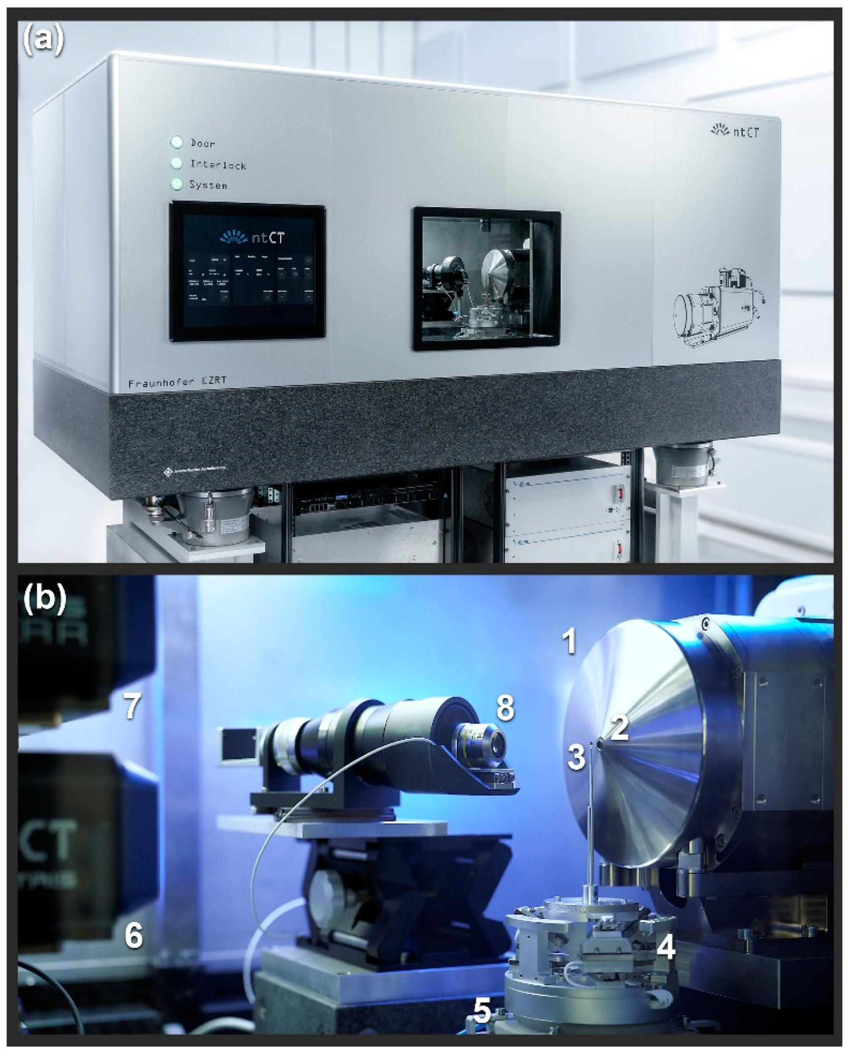
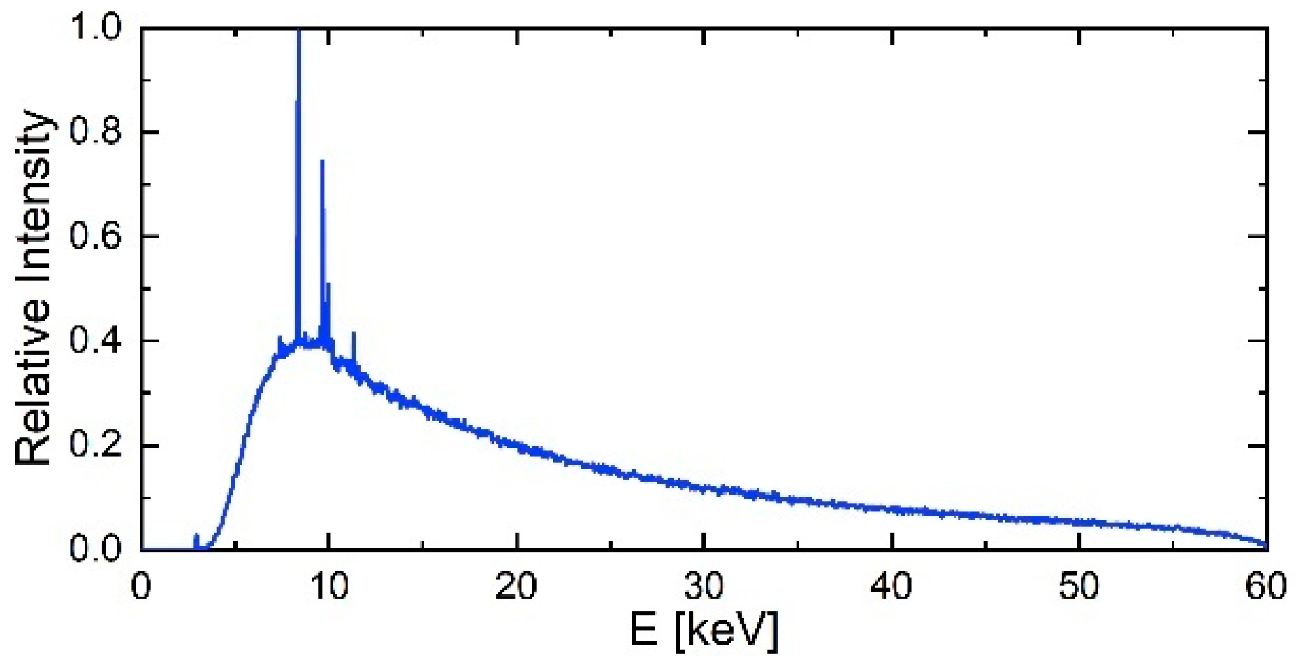
3. Experimental Setup

3.1. CT System

The employed device—the ntCT (Figure 1)—is a cooperative development of the University of Würzburg and the Fraunhofer EZRT and follows the principle of projection magnification. The utilized X-ray source is the Excillum Nanotube N2 60 kV (Excillum AB, Kista, Sweden) [10] with a 500 nm thick tungsten transmission target. According to the specifications, it achieves a 300 nm FWHM electron spot at 200 mW target. This information is consistent with our own investigations [31]. The source features an internal validation of the actual electron spot size as a measure of the achievable resolution. Figure 2 shows a simulated intensity spectrum of the X-rays. In particular, the significant fraction of photons with energies above 10 keV can be exploited in imaging, being advantageous compared to full-field microscopy.
A DECTRIS EIGER2 R (DECTRIS AG, Baden-Daettwil, Switzerland) [32] hybrid photon counting detector with a CdTe sensor is used for image acquisition. The detector’s active area consists of 2070 × 514 square pixels, each 75 µm wide. It possesses two variable energy thresholds so that only photons with an energy above the set level are counted simultaneously in two separate recordings. Based on the direct converting design, the detector has a high dynamic range due to the absent detector background and a high quantum efficiency of 0.9–1.0 (up to 25 keV), only limited by photons hitting edges and corners of pixels [33,34].
The positioning of the sample is realized by a 10-axes nano manipulator made of piezo stick-slip positioners with 6 degrees of freedom (DOF), including a high-precision air-bearing rotary table. A 3-axes manipulator made of linear spindle axes is used for placing the detector at distances between 250 mm to 650 mm from the source to set the magnification in a range from several micrometers down to 50 nm voxel sampling. Typical parameters for a CT scan are voxel samplings around 100 nm at 200 µm field of view (FOV) resulting in about 500 counts/(s∙pixel) at the detector. The entire system is packaged in a temperature-controlled double-walled radiation protection enclosure and sits vibration damped on a granite, to minimize movements due to drift or induced vibration during the measurement.

3.2. Sample and Measurement Preparation

Preferably, the diameter of the object is cut approximately to the desired field of view to avoid artifacts in the peripheral areas. The sample is then fixed on the tip of a needle-shaped sample holder, mounted on the manipulator and moved automatically to the examination position.
The reconstruction of the data is performed with a filtered back-projection methodology incorporating precise geometry information determined by prior calibration [37]. In this step, the measured data are also corrected for positional deviations which inevitably occur in nano CT scans, such as sample drift on the sub-micrometer scale and irregularities in detector pixel sensitivity. Depending on the sample, subsequent phase retrieval is applied.

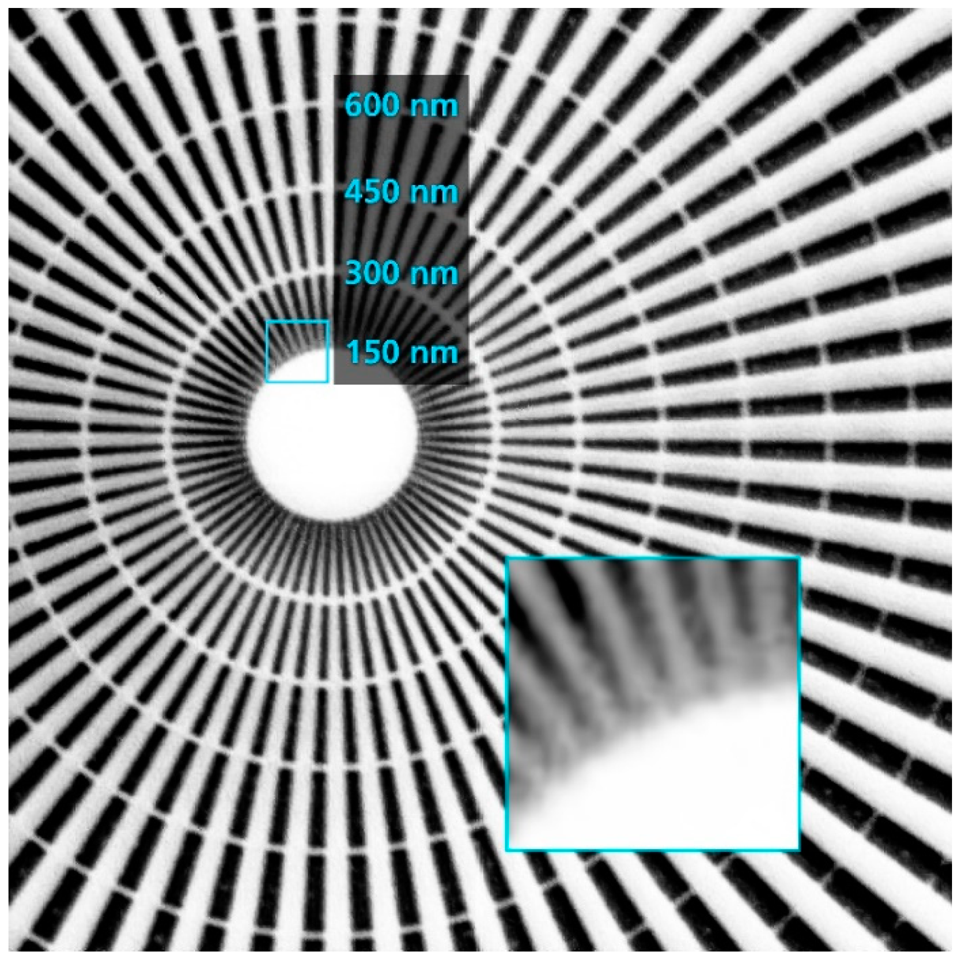
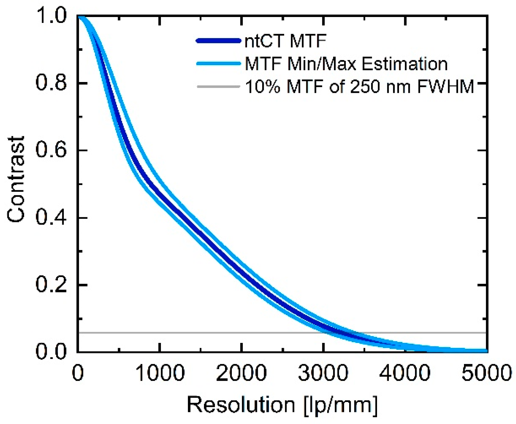
3.3. Validation of the Resolution

To evaluate the 2D resolution of the system, a Siemens star test pattern was inspected. This test pattern was located 160 µm in front of the 100 µm thick exit window of the source, with the detector positioned at a distance of 300 mm. This leads to a sampling of 71 nm. The Siemens star (ZonePlates Ltd., London, UK) consists of 1.5 µm lithographically etched tungsten and has the smallest structure size of 150 nm half period in the center.
To assess the obtained resolution in 3D, the measurements of the three samples shown were evaluated using the Fourier Shell Correlation (FSC) method [38]. (The FSC analysis and the calculation of the half-bit criterion were performed in Imagic FSC (Image Science Software GmbH, Berlin, Germany) [39]) Here, the FSC is a measure of the normalized cross-correlation between the spatial frequencies of two equivalent 3D datasets in Fourier space. To create these two datasets, the individual tomographies were divided equally (even and odd projections) and reconstructed separately. The achieved resolution is then obtained after the FSC comparison of the two volumes when reaching the half-bit criterion corresponding to the sample [40]. For visual confirmation of the resolution, the contrast in presumably periodic structures of the semiconductor sample was analyzed and then compared to the previous results.

3.4. Objects and Parameters for the Presented Sample Measurements

As the first sample, we show the internal structures of a commercially available semiconductor memory (SanDisk 32 GB micro SDHC UHS-I; Western Digital Ltd, Surrey, United Kingdom) [41,42]. Second, we display the active material phase LiNiCoAlO2-LiCoO2 of a commercial Kokam High-Energy 560 mA Pouch-Cell (Kokam, Suwon, Republic of Korea) [43]. Finally, we show a sample of a silicone-based conductive elastomer produced by Fraunhofer ISC Research Institute [27]. The material consists of a silicone elastomer matrix and is filled with 20 vol% flake-shaped particles of silver-coated copper (Cu/Ag-60/40). The highly anisotropic flakes have a thickness of approx. 100 nm, a diameter of approx. 4 µm and high electrical conductivity. Table 1 summarizes the recording parameters used for the individual measurements.

4. Results

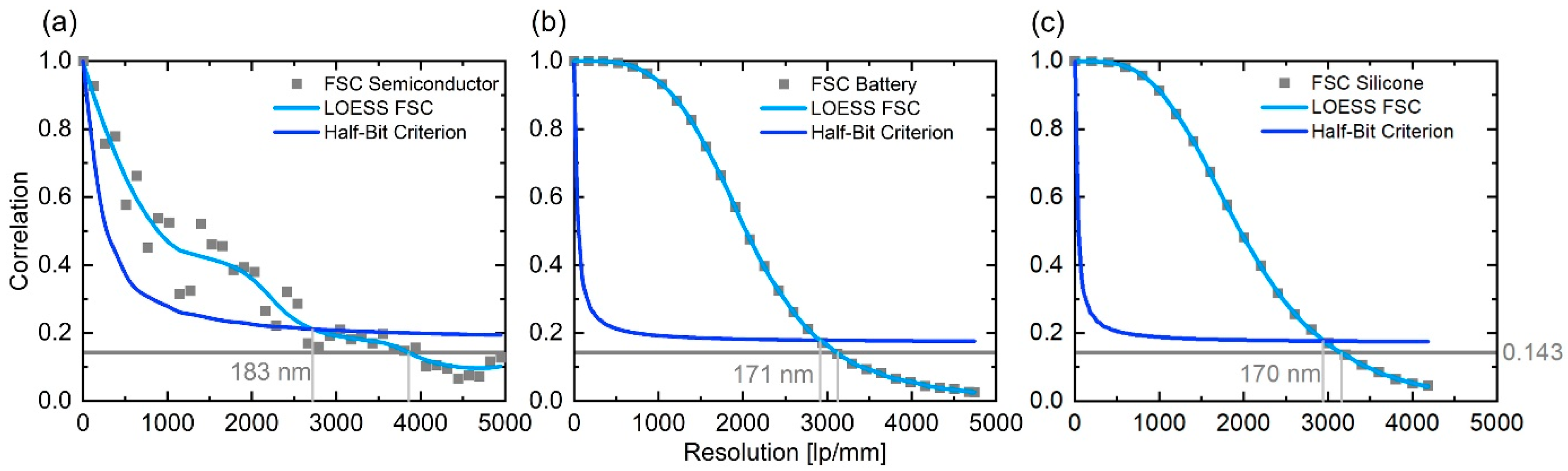
4.1. Resolution Evaluation

Figure 3 shows the background-corrected image of the Siemens star with an exposure time of 300 s. In the enlarged section, even the innermost lines with the highest spatial resolution of 3300 lp/mm (corresponding to 150 nm half period) are clearly visible.
To characterize the system’s modulation transfer function (MTF) as a more quantitative reference for the resolution, in a previous study we have already shown that the MTF of the imaging system (Figure 4) can be approximately described by the superposition of a Gaussian PSF with 250 nm full width at half maximum (FWHM) with an additional background of about 1.1 µm FWHM. This finding could be attributed to the characteristics of the X-ray source by further evaluating the shape of the electron beam on the target. For this purpose, the focus of the electron beam was manually scanned over edges on the patterned transmission target, to obtain an independent measure of the source point spread function by evaluating the radiation intensity measured in this process. For a more detailed description of the method, please refer to the previous study indicated [31]. For the visible resolution, which corresponds to the 10% MTF level, 3200 lp/mm is achieved with the high-resolution portion (narrow PSF). This is consistent with the visible 150 nm structures in the above-shown Siemens star image.
The 2D MTF defines the upper limit of the resolution achievable in tomographic imaging, which is subject to many other influencing factors such as the accuracy of the axes or drift in the individual components. To quantify the achieved resolution in 3D, the FSC was calculated from the volume data and plotted in Figure 5 together with the corresponding half-bit criterion.
The achieved resolution is in the range of 170–185 nm for all three samples and therefore confirms the expectation. The result of the conductive elastomer has to be considered with caution since the determined 170 nm are close to the sampling rate. However, the value matches the other results.
As an example of the achieved resolution, the local image contrast from the line profiles of the gray values over various structures marked in the section of the semiconductor scan was evaluated in Figure 6. In the adjacent plot, these points, which can be roughly assigned to the structure sizes 250 nm, 175 nm and 100 nm, were plotted against the MTF previously determined from the Siemens star. For simplicity and since we do not have the exact design parameters, we have assumed these structures to be periodic and with a regular duty cycle. It can be shown that the expected visibility of real structures in a sample can be confirmed.

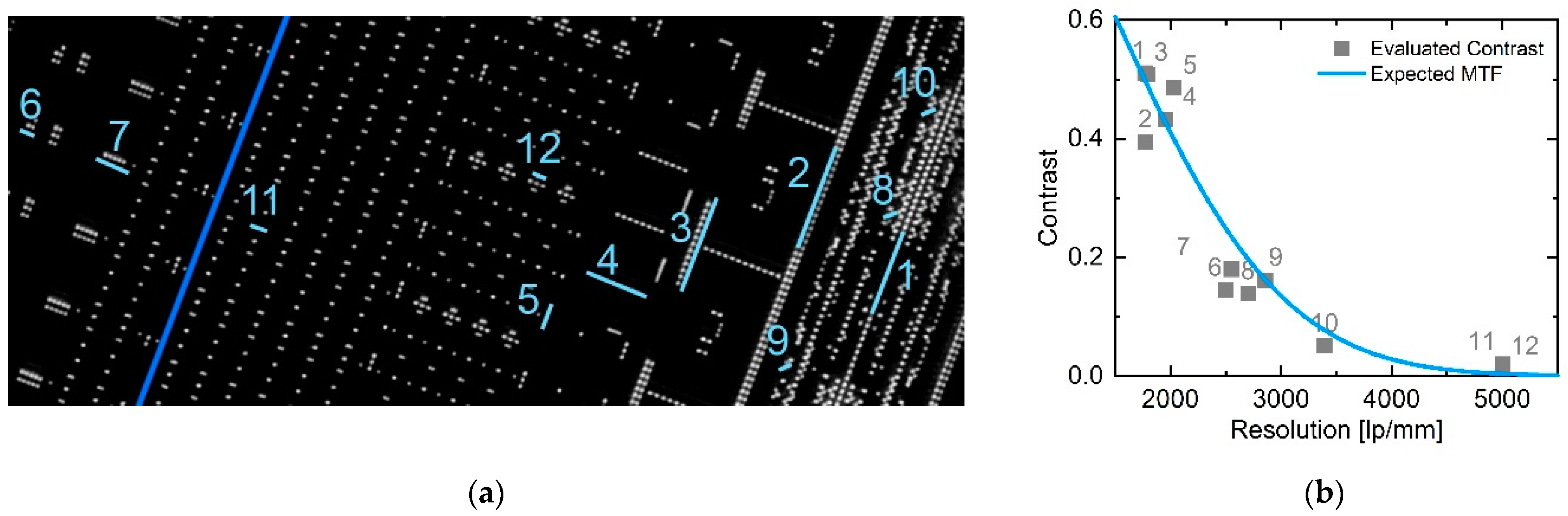
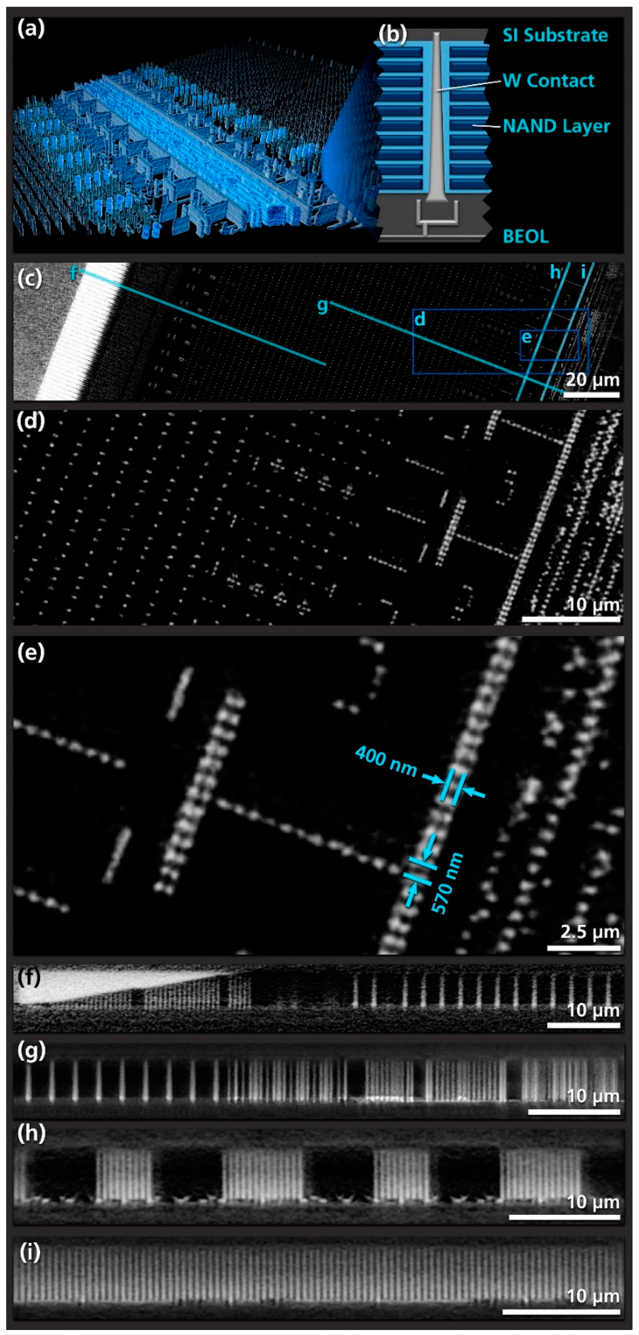
4.2. Semiconductor Sample

The reconstructed scan of the semiconductor memory chip is shown in Figure 7. The upper image (a) shows a 3D rendering of the sample volume. In particular, the tower-like contacts made of tungsten can be seen, which connect the 48 storage layers to the electronics. (b) shows a schematic enlargement of a single contact from the SI substrate. A cross-section of the volume and enlarged sections of it are shown in c-e. Based on publicly available information, these structures are expected to be between 100–200 nm [15,16,23,45,46]. In the enlarged view (e), two additional structure sizes were determined from the image and also specified. This fine, track-like structure consists of two rows of parallel plated-through contacts and has a period of 568 nm in length and 400 nm in lateral distance, corresponding to a frequency of 2500 lp/mm. Images (f–i) show various vertical sections through the volume as shown in (c). As expected from a commercial memory chip, the recognizable structures are uniform, parallel to each other and perpendicular to the other layers. There are also no other obvious defects visible in the metallization. Of particular interest is the visibility of the staircase structure typical for V-Nand memory [45,46,47] at the outer edge of the chip, as shown in (f). With a rising number of layers, the complexity of this staircase area increases, which is created in an elaborated multi-stage etching process. The exact positioning of the steps is necessary to contact the storage cells correctly [47].

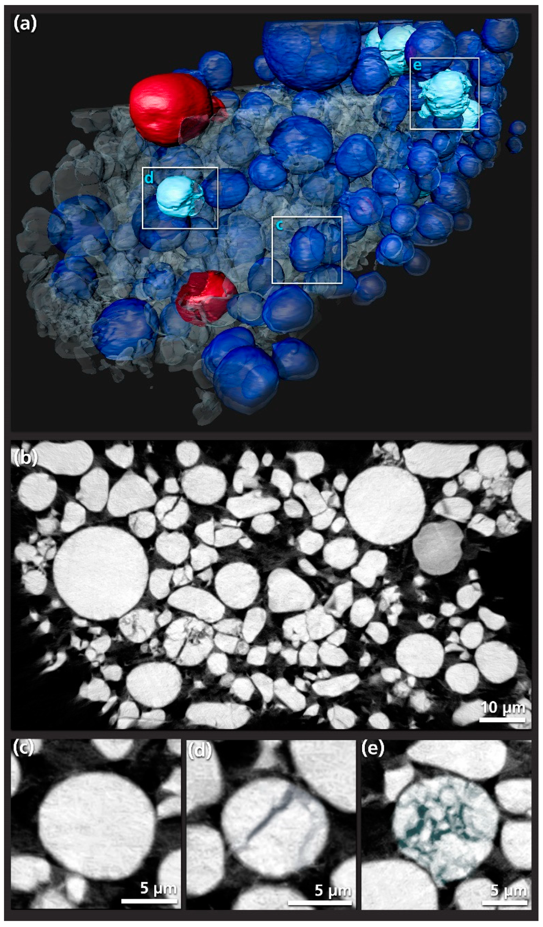
4.3. Battery Research

Figure 8 shows the reconstruction of the Li battery electrode. The three-dimensional rendering in (a) shows the shape and distribution of the active phases in the electrode. The corresponding false-color assignment to the expected components is based on the gray value, shape and structure of the individual particles. While typical spherical particles in the electrode are shown in blue, particles with already strong fragmentation inside are turquoise and the two red particles display a much weaker absorption and thus an untypical material composition. Picture (b) shows a single sectional view with scale bars for size allocation. Due to the wide field of view, it is possible to examine a large number of particles and the space between them in one measurement. Images (c–e) show enlarged sections of exemplarily chosen individual spherical particles in varying degrees of aging. (c) is in good condition as the majority of the sample, (d) shows already medium fissure as the first consequence of stress, and (e) shows an already heavily broken particle. These cracks are a clear sign of the structural degradation of a battery and occur as a result of mechanical or chemomechanical stress during the charging and discharging process. The desirable rapid charging operations, in particular, accelerate this process [25]. The detection and tracing of these cracks is an important approach in battery research in order to obtain information about the aging behavior and to develop long-lasting battery types.

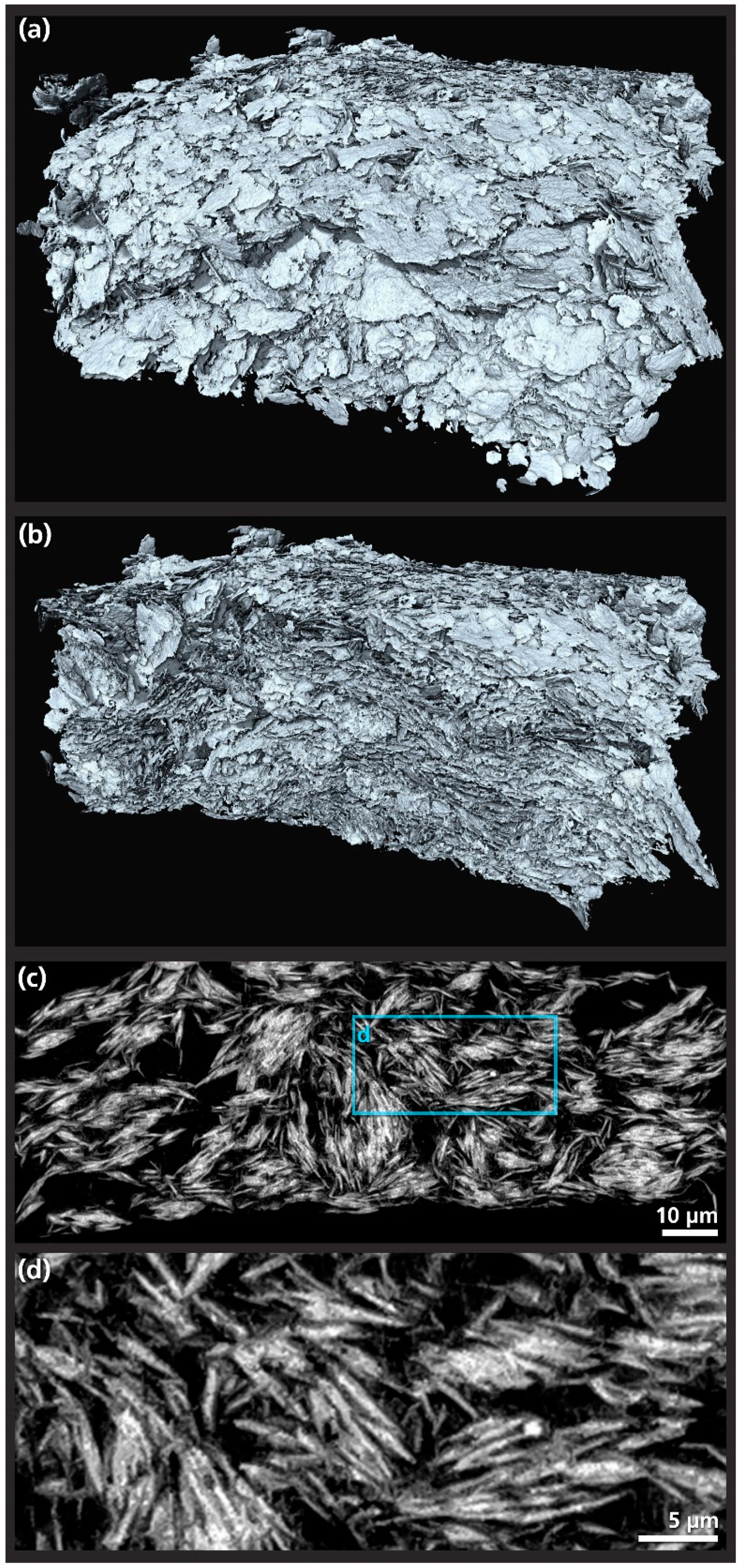
4.4. Functional Materials Development

The results of measuring the silicone polymer composite are shown in Figure 9. The picture in (a) shows the 3D-rendered volume of the segmented metal particles from the polymer composite. As stated earlier, it is necessary for the further development of this material class to obtain information on how the flake-shaped filler particles are distributed in the polymer matrix. In particular, the alignment of the particles to each other, directional effects from the production or agglomeration of the flakes have to be determined. It should be possible to make statements on the relative relationship of individual particles as well as to depict a sufficiently high number of particles to enable statistical evaluation and find percolation paths. In order to better access these properties visually, a volume section is shown in (b). Image (c) shows a sectional view of the sample. The sample has previously been subjected to a number of load cycles which led to a clearly visible agglomeration and local densification of the particles. Furthermore, an enlarged section is shown in (d), where the preferred arrangement in stacks and orientation in a horizontal direction is visible.
For the further improvement of the composite materials, it is necessary to achieve and prove a strain-stable and fatigue-resistant percolation of the particles. By visualizing a representative volume, nano CT analysis is a valuable tool for the further development of the material class of particle-filled polymer composites.

5. Conclusions

We presented the suitability and application of high-resolution nano CT with a nano focus source-based laboratory instrument for materials research. The lens-free setup based on projection magnification achieved a 2D resolution of 150 nm. The determined 3D resolution was only slightly inferior. Additionally, our analysis of the contrast in differently sized and presumably periodic structures in an SD card measurement confirms the shape of the system’s 2D MTF.
Overall, we demonstrated on the basis of three samples from current fields of research the suitability of the presented system and the potential merit of the laboratory-based nano CT analysis for materials research and development. We are capable of visualizing the 100–200 nm diameter through-silicon vias and examine them for defects such as misalignments or insufficient metallization. Therefore, the technology presented here will be a valuable tool for semiconductor research. In the high-energy lithium battery electrode, evidence of the battery’s performance level was found in the form of chemo-mechanically induced micro-cracks within the electrode particles. In this case, our large field of view enables statistical analysis. Finally, we demonstrated that for the conductive material composite, despite the highly absorbent material of the filler, the position and orientation of the particles can already be determined visually.

Author Contributions

Conceptualization, D.M. and C.F.; methodology, D.M., J.G., A.B., S.S. and C.F.; resources, D.M., J.G., A.B., S.S. and C.F.; investigation, D.M. and A.B.; data curation, D.M.; writing—original draft preparation, D.M.; writing—review and editing, D.M., J.G., A.B. and C.F.; visualization, D.M.; supervision, R.H.; project administration, C.F.; funding acquisition, R.H. and C.F. All authors have read and agreed to the published version of the manuscript.

Funding

This publication was supported by the Open Access Publication Fund of the University of Würzburg.

Data Availability Statement

The data that supports the findings in this study are available from the corresponding author upon reasonable request.

Acknowledgments

We would like to thank Jeffrey Gambino for his expertise and advice on the interpretation of the shown semiconductor structures.

Conflicts of Interest

The authors declare no conflict of interest.

References

  1. Falcone, R.; Jacobsen, C.; Kirz, J.; Marchesini, S.; Shapiro, D.; Spence, J. New directions in X-ray microscopy. Contemp. Phys. 2011, 52, 293–318. [Google Scholar] [CrossRef]
  2. Sakdinawat, A.; Attwood, D. Nanoscale X-ray imaging. Nat. Photonics 2010, 4, 840–848. [Google Scholar] [CrossRef]
  3. Fella, C.; Balles, A.; Hanke, R.; Last, A.; Zabler, S. Hybrid setup for micro- and nano-computed tomography in the hard X-ray range. Rev. Sci. Instrum. 2017, 88, 123702. [Google Scholar] [CrossRef]
  4. TriLambda 40nm X-ray Microscope—Sigray. Available online: http://www.sigray.com/trilambda (accessed on 27 August 2020).
  5. ZEISS Xradia 810 Ultra—Highest Spatial Resolution Lab-Based XRM. Available online: https://www.zeiss.com/microscopy/int/products/x-ray-microscopy/xradia-810-ultra.html (accessed on 27 August 2020).
  6. Stahlhut, P.; Ebensperger, T.; Zabler, S.; Hanke, R. A laboratory X-ray microscopy setup using a field emission electron source and micro-structured reflection targets. Nucl. Instruments Methods Phys. Res. Sect. B Beam Interact. with Mater. Atoms 2014, 324, 4–10. [Google Scholar] [CrossRef]
  7. Stahlhut, P.; Dremel, K.; Dittmann, J.; Engel, J.M.; Zabler, S.; Hoelzing, A.; Hanke, R. First Results on Laboratory Nano-CT with a Needle Reflection Target and an Adapted Toolchain. In Proceedings of the Developments in X-ray Tomography X; Stock, S.R., Müller, B., Wang, G., Eds.; SPIE: San Diego, CA, USA, 2016; Volume 9967, p. 99670I. [Google Scholar]
  8. Sasov, A.; Pauwels, B.; Bruyndonckx, P. New Type of X-Ray Source for Lensless Laboratory Nano-CT with 50-nm Resolution. In Proceedings of the Developments in X-ray Tomography VII; Stock, S.R., Ed.; SPIE: San Diego, CA, USA, 2010; Volume 7804, p. 78040Q. [Google Scholar]
  9. Nachtrab, F.; Firsching, M.; Uhlmann, N.; Speier, C.; Takman, P.; Tuohimaa, T.; Heinzl, C.; Kastner, J.; Larsson, D.H.; Holmberg, A.; et al. NanoXCT: Development of a laboratory nano-CT system. Dev. X-Ray Tomogr. IX 2014, 9212, 92120L. [Google Scholar] [CrossRef]
  10. NanoTube N2 60 kV—Excillum. Available online: https://www.excillum.com/products/nanotube/nanotube-n2-60kv/ (accessed on 27 August 2020).
  11. Fella, C.; Dittmann, J.; Muller, D.; Donath, T.; Murer, D.; Tuohimaa, T.; Sofiienko, A.; Zabler, S.; Hanke, R. Implementation of a Computed Tomography System based on a laboratory-based nanofocus X-ray source. Microsc. Microanal. 2018, 24, 236–237. [Google Scholar] [CrossRef] [Green Version]
  12. Müller, M.; de Sena Oliveira, I.; Allner, S.; Ferstl, S.; Bidola, P.; Mechlem, K.; Fehringer, A.; Hehn, L.; Dierolf, M.; Achterhold, K.; et al. Myoanatomy of the velvet worm leg revealed by laboratory-based nanofocus X-ray source tomography. Proc. Natl. Acad. Sci. USA 2017, 114, 12378–12383. [Google Scholar] [CrossRef] [PubMed] [Green Version]
  13. Aryan, P.; Sampath, S.; Sohn, H. An overview of non-destructive testing methods for integrated circuit packaging inspection. Sensors 2018, 18, 1981. [Google Scholar] [CrossRef] [Green Version]
  14. Gambino, J.P.; Adderly, S.A.; Knickerbocker, J.U. An overview of through-silicon-via technology and manufacturing challenges. Microelectron. Eng. 2015, 135, 73–106. [Google Scholar] [CrossRef]
  15. Micheloni, R.; Crippa, L.; Zambelli, C.; Olivo, P. Architectural and integration options for 3D NAND flash memories. Computers 2017, 6, 27. [Google Scholar] [CrossRef]
  16. Tech Brief: Memory “Grows Up” with 3D NAND|Lam Research. Available online: https://blog.lamresearch.com/tech-brief-memory-grows-up-with-3d-nand/ (accessed on 27 August 2020).
  17. Overcoming Challenges in 3D NAND Volume Manufacturing|Lam Research. Available online: https://blog.lamresearch.com/overcoming-challenges-in-3d-nand-volume-manufacturing/ (accessed on 27 August 2020).
  18. Tanaka, H.; Kido, M.; Yahashi, K.; Oomura, M.; Katsumata, R.; Kito, M.; Fukuzumi, Y.; Sato, M.; Nagata, Y.; Matsuoka, Y.; et al. Bit Cost Scalable Technology with and Plug Process for Ultra High Density Flash Memory. In Proceedings of the Digest of Technical Papers—Symposium on VLSI Technology, Kyoto, Japan, 12–14 June 2007; pp. 14–15. [Google Scholar]
  19. Sakuma, K.; Andry, P.S.; Tsang, C.K.; Wright, S.L.; Dang, B.; Patel, C.S.; Webb, B.C.; Maria, J.; Sprogis, E.J.; Kang, S.K.; et al. 3D chip-stacking technology with through-silicon vias and low-volume lead free interconnections. IBM J. Res. Dev. 2008, 52, 611–622. [Google Scholar] [CrossRef]
  20. Kong, L.W.; Lloyd, J.R.; Liehr, M.; Rudack, A.C.; Arkalgud, S.; Diebold, A.C. Measuring thermally induced void growth in conformally filled through-silicon vias (TSVs) by laboratory x-ray microscopy. Metrol. Insp. Process Control Microlithogr. XXVI 2012, 8324, 832412. [Google Scholar] [CrossRef]
  21. Sekhar, V.N.; Neo, S.; Yu, L.H.; Trigg, A.D.; Kuo, C.C. Non-destructive testing of a high dense small dimension through silicon via (TSV) array structures by using 3D X-ray computed tomography method (CT scan). In Proceedings of the 2010 12th Electronics Packaging Technology Conference, EPTC 2010, Singapore, 8–10 December 2010; pp. 462–466. [Google Scholar]
  22. Gambino, J.P.; Bowe, W.; Bronson, D.M.; Adderly, S.A. Imaging of through-silicon vias using X-Ray computed tomography. Proc. Int. Symp. Phys. Fail. Anal. Integr. Circuits IPFA 2014, 327–331. [Google Scholar] [CrossRef]
  23. Nowakowski, P.; Ray, M.; Fischione, P.; Sagar, J. Top-down delayering by low energy, broad-beam, argon ion milling—A solution for microelectronic device process control and failure analyses. In Proceedings of the 2017 28th Annual SEMI Advanced Semiconductor Manufacturing Conference (ASMC), Saratoga Springs, NY, USA, 15–18 May 2017; pp. 95–101. [Google Scholar] [CrossRef]
  24. Bak, S.M.; Shadike, Z.; Lin, R.; Yu, X.; Yang, X.Q. In situ/operando synchrotron-based X-ray techniques for lithium-ion battery research. NPG Asia Mater. 2018, 10, 563–580. [Google Scholar] [CrossRef] [Green Version]
  25. Yang, Y.; Xu, R.; Zhang, K.; Lee, S.; Mu, L.; Liu, P.; Waters, C.K.; Spence, S.; Xu, Z.; Wei, C.; et al. Quantification of Heterogeneous Degradation in Li-Ion Batteries. Adv. Energy Mater. 2019, 9, 1900674. [Google Scholar] [CrossRef]
  26. Xu, R.; Yang, Y.; Yin, F.; Liu, P.; Cloetens, P.; Liu, Y.; Lin, F.; Zhao, K. Heterogeneous damage in Li-ion batteries: Experimental analysis and theoretical modeling. J. Mech. Phys. Solids 2019, 129, 160–183. [Google Scholar] [CrossRef]
  27. Böse, H.; Uhl, D. Dielectric Elastomers with Novel Highly-Conducting Electrodes. In Proceedings of the Electroactive Polymer Actuators and Devices (EAPAD) 2013; Bar-Cohen, Y., Ed.; SPIE: San Diego, CA, USA, 2013; Volume 8687, p. 86872O. [Google Scholar]
  28. Yamaguchi, K.; Busfield, J.J.C.; Thomas, A.G. Electrical and mechanical behavior of filled elastome. I. The effect of strain. J. Polym. Sci. Part B Polym. Phys. 2003, 41, 2079–2089. [Google Scholar] [CrossRef]
  29. Busfield, J.J.C.; Thomas, A.G.; Yamaguchi, K. Electrical and mechanical behavior of filled rubber. III. Dynamic loading and the rate of recovery. J. Polym. Sci. Part B Polym. Phys. 2005, 43, 1649–1661. [Google Scholar] [CrossRef]
  30. Staniewicz, L.; Vaudey, T.; Degrandcourt, C.; Couty, M.; Gaboriaud, F.; Midgley, P. Electron tomography provides a direct link between the Payne effect and the inter-particle spacing of rubber composites. Sci. Rep. 2014, 4, 1–7. [Google Scholar] [CrossRef] [Green Version]
  31. Graetz, J.; Müller, D.; Balles, A.; Fella, C. Lenseless X-ray nano-tomography down to 150 nm resolution: On the quantification of modulation transfer and focal spot of the lab-based ntCT system. J. Instrum. 2021, 16, P01034. [Google Scholar] [CrossRef]
  32. EIGER2 R for Laboratory—Dectris. Available online: https://www.dectris.com/products/eiger2/eiger2-r-for-laboratory/ (accessed on 28 December 2020).
  33. Förster, A.; Brandstetter, S.; Schulze-Briese, C. Transforming X-ray detection with hybrid photon counting detectors. Philos. Trans. R. Soc. A Math. Phys. Eng. Sci. 2019, 377, 20180241. [Google Scholar] [CrossRef]
  34. Zambon, P.; Radicci, V.; Trueb, P.; Disch, C.; Rissi, M.; Sakhelashvili, T.; Schneebeli, M.; Broennimann, C. Spectral response characterization of CdTe sensors of different pixel size with the IBEX ASIC. Nucl. Instrum. Methods Phys. Res. Sect. A Accel. Spectrometers Detect. Assoc. Equip. 2018, 892, 106–113. [Google Scholar] [CrossRef]
  35. Roberts, T.J.; Kaplan, D.M. G4beamline simulation program for matter-dominated beamlines. In Proceedings of the 2007 IEEE Particle Accelerator Conference (PAC), Albuquerque, NM, USA, 25–19 June 2007; pp. 3468–3470. [Google Scholar] [CrossRef]
  36. Agostinelli, S.; Allison, J.; Amako, K.; Apostolakis, J.; Araujo, H.; Arce, P.; Asai, M.; Axen, D.; Banerjee, S.; Barrand, G.; et al. GEANT4—A simulation toolkit. Nucl. Instrum. Methods Phys. Res. Sect. A Accel. Spectrometers Detect. Assoc. Equip. 2003, 506, 250–303. [Google Scholar] [CrossRef] [Green Version]
  37. Graetz, J. Auto-calibration of cone beam geometries from arbitrary rotating markers using a vector geometry formulation of projection matrices. Phys. Med. Biol. 2021, 66, 75013. [Google Scholar] [CrossRef] [PubMed]
  38. van Heel, M.; Schatz, M. Reassessing the Revolution’s Resolutions. BioRxiv 2017, 224402. [Google Scholar] [CrossRef]
  39. Image Science—FSC Program. Available online: https://www.imagescience.de/fsc.html (accessed on 9 February 2021).
  40. Van Heel, M.; Schatz, M. Fourier shell correlation threshold criteria. J. Struct. Biol. 2005, 151, 250–262. [Google Scholar] [CrossRef]
  41. Toshiba: News Release (4 August 2015): Toshiba Develops World’s First 256Gb, 48-layer BiCS FLASHTM. Available online: https://www.toshiba.co.jp/about/press/2015_08/pr0401.htm (accessed on 27 August 2020).
  42. Toshiba and SanDisk Announce 48-layer 256Gbit TLC 3D NAND. Available online: https://www.anandtech.com/show/9490/toshiba-and-sandisk-announce-48layer-256gbit-tlc-3d-nand (accessed on 27 August 2020).
  43. Almar, L.; Joos, J.; Weber, A.; Ivers-Tiffée, E. Microstructural feature analysis of commercial Li-ion battery cathodes by focused ion beam tomography. J. Power Sources 2019, 427, 1–14. [Google Scholar] [CrossRef]
  44. Schindelin, J.; Rueden, C.T.; Hiner, M.C.; Eliceiri, K.W. The ImageJ ecosystem: An open platform for biomedical image analysis. Mol. Reprod. Dev. 2015, 82, 518–529. [Google Scholar] [CrossRef] [Green Version]
  45. 3D NAND: Challenges beyond 96-Layer Memory Arrays|Coventor. Available online: https://www.coventor.com/blog/3d-nand-challenges-beyond-96-layer-memory-arrays/ (accessed on 27 August 2020).
  46. Singh, H. Overcoming challenges in 3D NAND volume manufacturing. Solid State Technol. 2017, 60, 18–21. [Google Scholar]
  47. Advanced Patterning Techniques For 3D NAND Devices. Available online: https://semiengineering.com/advanced-patterning-techniques-for-3d-nand-devices/ (accessed on 27 August 2020).
Figure 1. Image and description of the main components of the used system. (a) Exterior view of the system with a temperature-controlled lead booth and air-bearing granite for vibration damping. (b) Inside view into the device with: 1. nano focus X-ray source, 2. exit window and at the same time tungsten transmission target on a diamond substrate, 3. sample mounted on a needle-shaped holder, 4. 6-DOF hexapod made of piezo linear axes for fine adjustment of the sample on the rotation axis, 5. air-bearing rotary stage (and in the picture not visible below three further linear axes for positioning of the sample holder), 6. DECTRIS EIGER2 R CdTe detector on 3 linear axes, 7. DECTRIS detector with SI sensor, and 8. optical microscope to support the sample adjustment.
Crystals 11 00677 g001
Figure 2. Monte Carlo simulated intensity spectrum of X-rays from the nano focus source used, considering the real geometry (exit window and air absorption for 280 mm detector distance). Simulation performed in G4beamline 3.06 [35], based on GEANT4 [36].
Crystals 11 00677 g002
Figure 3. Siemens star test pattern with 300 s exposure time. Inner structure with 150 nm lines and spaces are clearly visible.
Crystals 11 00677 g003
Figure 4. 2D MTF graph derived from the Siemens star image. As the electron spot in the source can be approximately described by the superposition of a narrow and a wide focal spot, the MTF is also composed of a high-frequency contribution (corresponding to 250 nm point spread FWHM) and a low-frequency background share (corresponding to 1.1 µm point spread FWHM) [31].
Crystals 11 00677 g004
Figure 5. FSC curves of the three samples shown below, (a) the semiconductor memory, (b) the lithium battery and (c) the conductive elastomer, and the corresponding half-bit criterion curves plotted versus spatial resolution. The FSC data were smoothed with a LOESS algorithm. The intersection points between both curves are shown in each case. Additionally, the less valid 1/7 level is plotted. The achieved resolutions are in the range of 170–185 nm and thus confirm the determined 2D resolution.
Crystals 11 00677 g005
Figure 6. Application of the local image contrast ratio at different structures in the horizontal section of the semiconductor memory dataset (a) which are assumed to be approximately periodic and comparison with the previously determined MTF (b). (All sectional images shown were exported with ImageJ Fiji [44]. Additionally in this software, the local contrast was extracted as a line profile of the gray values over the selected structure) The corresponding areas in the image are marked accordingly. Points 11 and 12 are roughly on a par with an expectable noise level and should therefore only be evaluated as image contrast with caution.
Crystals 11 00677 g006
Figure 7. Reconstructed nano CT scan of a semiconductor memory chip from a commercial micro sd card (SanDisk 32 GB microSDHC UHS-I) measured with a sampling of 98 nm. (a) 3D rendering (All 3D visualizations shown in this study were carried out in Avizo 9.0—Thermo Fisher Scientific) of the internal metalized structures, where the individual contacts with an expected size between 100–200 nm can be clearly identified. (b) schematic of a single contact pillar connecting the multiple word lines. (c) volume cross-section from the reconstruction with a memory array in the center and a section of the peripheral circuits to the right. (d,e) enlarged details of the sectional view with dimensions for specific features, (fi) vertical sections through the volume corresponding to the markings in (c). (f) word line staircase at the edge of the chip. (h,i) vertical view of the peripheral circuits.
Crystals 11 00677 g007
Figure 8. Reconstruction of the high-resolution nano CT measurement of the electrode of a commercial lithium pouch-cell with 105 nm sampling. (a) 3D rendering of the sample. Typical spherical particles in the electrode are shown in blue, spherical particles with an already strong fragmentation inside are turquoise, the two red particles have a much weaker absorption and seem to have a different material composition. (b) unrendered sectional image from the reconstructed volume to obtain an overview of the aging state. (ce) enlarged sections of individual spherical particles. (c) in good condition as the majority of the sample. (d) medium fissure as the first consequence of mechanical or chemomechanical stress. (e) already heavily broken particle.
Crystals 11 00677 g008
Figure 9. Reconstruction of the nano CT scan of the functional material composite. (a) 3D rendering of the whole reconstructed sample consisting of a flat cuboid with an edge length of about 100 µm. The rendering focuses on the metallic filler, whose orientation is essential for the function of the material. (b) sliced sample from the above rendering in which the self-organized alignment of the filler can be seen. (c) sectional image from the reconstruction, demonstrating that the particles have aggregated and locally compressed during the cyclic loading. (d) enlarged detail of the sectional image.
Crystals 11 00677 g009
Table 1. Overview of acquisition parameters for the shown computed tomography measurements with source object distance (SOD), source-detector distance (SDD), number of exposures, effective sampling size, single image exposure time, detector threshold window (upper and lower threshold), power on the X-ray target and acceleration voltage.
SampleGeneral SettingsDetectorSource
SODSDDRecordingsSamplingExposure TimeThreshold WindowTarget PowerVoltage
Semiconductor0.80 mm575 mm280098 nm15 s5–60 keV165 mW60 kV
Li-Battery0.63 mm425 mm3600105 nm30 s5–60 keV67 mW60 kV
Elastomer0.46 mm280 mm2400119 nm10 s8–60 keV160 mW60 kV
Publisher’s Note: MDPI stays neutral with regard to jurisdictional claims in published maps and institutional affiliations.

