
A Phononic Crystal with Differently Configured Double Defects for Broadband Elastic Wave Energy Localization and Harvesting


1
Department of Mechanical Engineering, Seoul National University, Seoul 08826, Korea
2
Institute of Advanced Machines and Design, Seoul National University, Seoul 08826, Korea
3
OnePredict Inc., Seoul 06160, Korea
*
Author to whom correspondence should be addressed.
Crystals 2021, 11(6), 643; https://doi.org/10.3390/cryst11060643
Submission received: 16 May 2021
/
Revised: 2 June 2021
/
Accepted: 3 June 2021
/
Published: 5 June 2021
(This article belongs to the Special Issue Applications of Phononic Crystals & Acoustic Metamaterials)
Abstract
:Several previous studies have been dedicated to incorporating double defect modes of a phononic crystal (PnC) into piezoelectric energy harvesting (PEH) systems to broaden the bandwidth. However, these prior studies are limited to examining an identical configuration of the double defects. Therefore, this paper aims to propose a new design concept for PnCs that examines differently configured double defects for broadband elastic wave energy localization and harvesting. For example, a square-pillar-type unit cell is considered and a defect is considered to be a structure where one piezoelectric patch is bonded to a host square lattice in the absence of a pillar. When the double defects introduced in a PnC are sufficiently distant from each other to implement decoupling behaviors, each defect oscillates like a single independent defect. Here, by differentiating the geometric dimensions of two piezoelectric patches, the defects’ dissimilar equivalent inertia and stiffness contribute to individually manipulating defect bands that correspond to each defect. Hence, with adequately designed piezoelectric patches that consider both the piezoelectric effects on shift patterns of defect bands and the characteristics for the output electric power obtained from a single-defect case, we can successfully localize and harvest the elastic wave energy transferred in broadband frequencies.
1. Introduction
In the last decade, piezoelectric energy harvesting (PEH) that incorporates phononic crystals (PnCs) has drawn growing interest as a breakthrough technology to amplify the amount of input mechanical energy fed into piezoelectric materials [1,2,3,4,5]. PEH technology, which scavenges usable electricity from ambient, otherwise wasted, mechanical vibrations, and/or waves generated in engineered systems via direct piezoelectric effects, has attracted much attention as an alternative to chemical batteries as a way to offer sustainable electric power to small electronic devices, such as Internet-of-Things sensors [6,7,8,9]. However, conventional PEH [10,11,12,13,14] has struggled from the fact that the harvestable electric power is inevitably insufficient when input mechanical energy is small. Motivated by this, PnCs’ distinctive characteristics of tailoring elastic wave energy toward a wanted location open up new avenues in the PEH research area.
PnCs, a new type of advanced functional structure, made up of a periodic array of repetitive unit cells [15], enable the realization of extraordinary wave phenomena (e.g., negative refraction [16], gradient refractive index [17], zero reflective index [18], and self-collimation [19]) that are beyond the physical properties exhibited by natural media. One representative phenomenon displayed by PnCs is defect-mode-induced energy localization [20,21,22,23]. When a unit cell lies at the scale of the wavelength of the propagating elastic waves, due to destructive interferences resulting from unit cells’ periodicity, Bragg scattering gives rise to the emergence of phononic band gaps (PBGs) in the dispersion curves of the PnC [24,25]. PBGs play a role in banning incident elastic waves from being propagated [26,27]. Here, a fascinating phenomenon is observed when a defect, a disordering structure that locally disturbs the periodicity, is deliberately introduced within the PnC. The imposition of the defect contributes to the generation of flat passbands, called defect bands, within the PBGs [28,29]. Due to the mechanically resonating characteristics of the defect, these defect bands feature the confinement of incident elastic wave energy inside the defect [30,31]. Hence, as compared to a case in the absence of the defect-introduced PnC, a piezoelectric patch inside the defect can achieve high amplification of the output electric power via defect-mode-enabled energy localization.
Several prior efforts have been dedicated to analytical/numerical modeling [32,33,34] and experimental demonstrations [35,36,37] of enhanced PEH strategies that leverage a PnC with a single defect. However, inherent challenges exist in that the bandwidth for PEH is considerably narrow, since the defect-mode-induced energy localization and harvesting approaches examined in previous research can be performed only at a single defect band frequency. To address this issue, Jo et al. [38] pushed the boundaries of the design space of PEH systems by proposing, for the first time, a double-defects-introduced PnC. When closely located double defects were created in a PnC, an unusual phenomenon, splitting of defect bands obtained from a single defect, took place due to coupling between the defects. In this context, the feasibility of broadband energy localization and harvesting was initiated. Furthermore, Jo et al. [39] proposed a new design concept: a graded PnC with decoupled double defects. When gradually changing the geometry of unit cells in a particular arranging direction, the decoupled double defects represented different, but independent, defect bands and realized broadband PEH. However, both of these studies of double-defect-introduced PnCs limited their designs to an identical configuration of the double defects. To date, the incorporation of a PnC with differently patterned double defects and a PEH system for broad bandwidth purposes has not yet been explored.
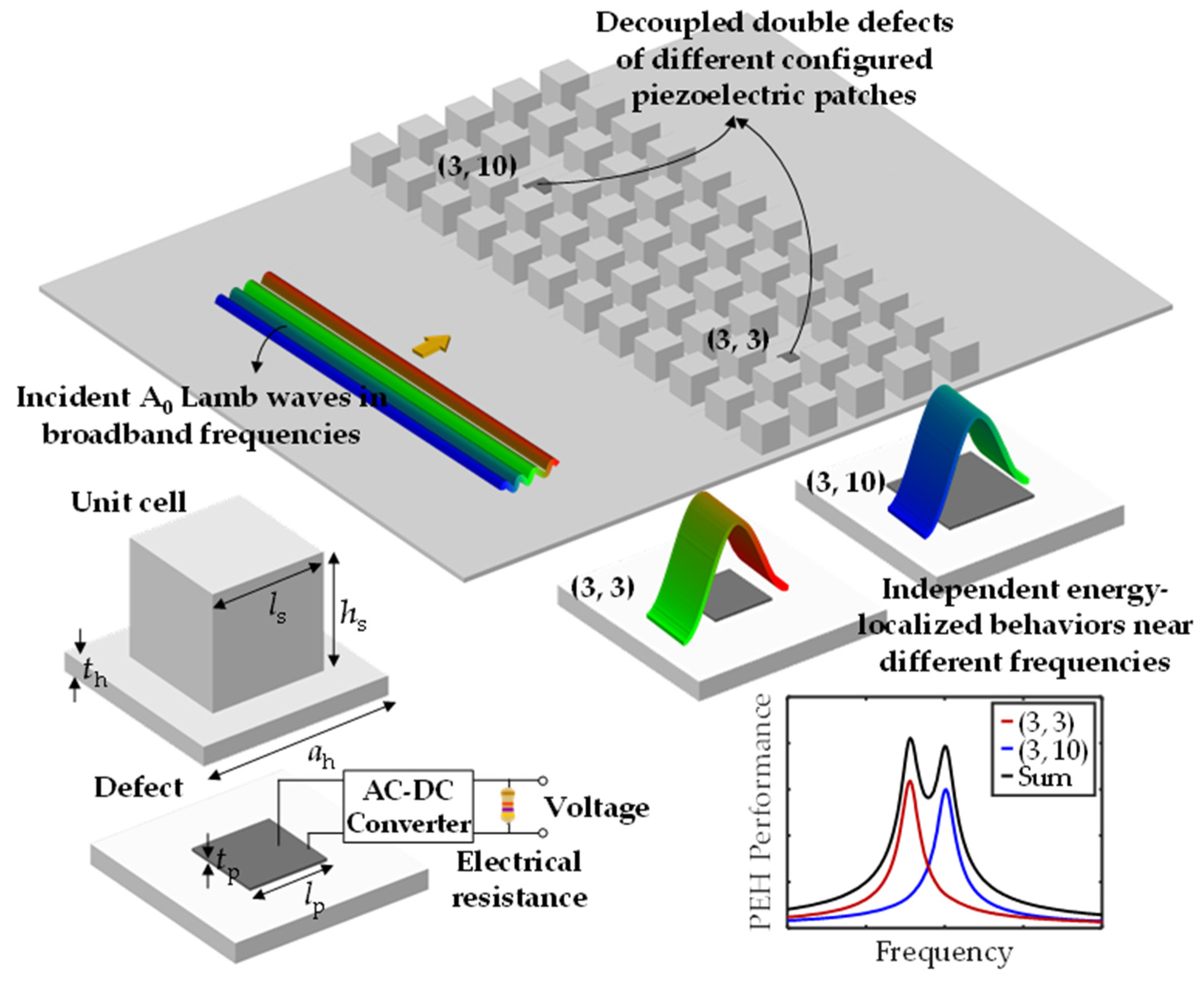
Therefore, the research outlined in this paper aims to propose a new design concept: a PnC with differently configured—as well as decoupled—double defects for broadband elastic wave energy localization and harvesting purposes. Figure 1 illustrates the schemes of how the proposed PnC concept enables broadband PEH. For the periodically arranged square–pillar-type unit cells in the two-dimensional space, double defects are imposed in the manner of eliminating two pillars and attaching one square piezoelectric patch to each lattice. The defects are far enough away from each other to assure the decoupling characteristic; thus, each defect behaves like a single independent defect. Here, when the piezoelectric patches have distinct geometric dimensions, the defects’ dissimilar equivalent mass and stiffness contribute to the formation of distinguished but independent defect bands, thanks to the decoupling property. Hence, by properly spacing the independent frequency response functions (FRFs) for PEH performance of well-designed patches, we can successfully harvest, as well as localize, the elastic wave energy transferred in broadband frequencies. Compared with the conventional approach of a graded PnC with decoupled double defects, the benefit of the proposed design concept is that it facilitates the manipulation of decoupled defect bands (e.g., values and their difference) by adjusting the geometry of additional attached piezoelectric patches, even if the unit cells have already been specified.
2. System Configuration and Numerical Simulation Settings
The PnC-inspired PEH system under consideration is outlined in Figure 1. The unit cell consists of an aluminum square lattice, where an aluminum square pillar adheres to the top surface; the square pillar is placed in the center of the lattice. The PnC is constituted by a 5 × 12 arrangement of the unit cells. At the same time, two square pillars in the locations of (3, 3) and (3, 10) are removed, and square piezoelectric patches (colored in dark-gray) of PZT-5H (lead zirconate titanate, Pb(ZrxTi1−x)O3) with different geometric dimensions are bonded to the top surface of each aluminum lattice. An alternating-current-to-direct-current (AC-DC) converter and an external electrical resistance are connected to each piezoelectric patch. In this paper, the two square lattices with the attached piezoelectric patches are called double defects. Here, Sx and Sy in an array Sx × Sy refer to the number of unit cells along the x- and y-directions; the notation (m, n) stands for a particular location in the m-th unit cell along the x-direction and the n-th unit cell along the y-direction. Note that Jo et al. showed that (1) there exists an optimum defect location for maximum output electric power amplification [40] and (2) double defects in a PnC are decoupled and exhibit independent energy-localized behaviors when they are sufficiently remote from each other [39]. Through preliminary parametric studies of the considered PnC, we found that (1) the 3rd-layer in the x-direction was suitable for highly dense PEH and (2) the defect locations of (3, 3) and (3, 10) were enough for decoupling.
The material properties of the aluminum and PZT-5H are as follows [41,42]. The mass density, Young’s modulus, and Poisson’s ratio of the aluminum are 2700 kg/m3, 70 GPa, and 0.33, respectively. For the PZT-5H, the mass density is 7500 kg/m3; the elastic constants , , , , , and at a constant electric field are 127 GPa, 80.2 GPa, 84.6 GPa, 117 GPa, 23.0 GPa, and 23.5 GPa, respectively; the piezoelectric coefficients e31, e33, and e15 are −6.62 C/m2, 23.2 C/m2, and 17.0 C/m2, respectively; dielectric permittivities and at a constant strain are 15.1 nF/m and 12.7 nF/m, respectively. Overall the structure, a light loss factor of 0.001 was considered. Geometric parameters in the PnC are outlined as follows. The lattice constant ah and thickness th of the host plate in the unit cell are 20 mm and 2 mm, respectively. Both the length ls and height hs of the square pillar in the unit cell are 12 mm. The lengths lp(3,3) and lp(3,10) of the square piezoelectric patches at (3, 3) and (3, 10) are 6 mm and 9 mm, respectively. The thickness tp of both patches is 0.3 mm. The reason for selecting these values was to harvest elastic wave energy propagating around 80 kHz. The size of the piezoelectric patches was determined through parametric studies that considered both (1) the piezoelectric effects on shift patterns of defect bands and (2) the PEH bandwidth obtained from a single-defect case; each detailed description is available in Section 3.1 and Section 3.2, respectively. The target frequency range may be altered; however, it should be noted that the physical phenomenon to be observed is still valid no matter what geometry or material properties of pillars and piezoelectric patches are used.
For the numerical model, a commercial finite-element-based tool, Comsol Multiphysics 5.5, was used. Comsol Multiphysics has been broadly employed in evaluating the output performances of PEH of PnC-induced systems, since its numerical simulations have presented results consistent with experiments [43,44,45,46]. The PnC lays in the engineering situation where the incident A0 (the lowest antisymmetric) Lamb waves came from the left domain with a specified velocity amplitude of 15.08 mm/s. Note that the input velocity amplitude was calculated by 2π × (frequency) × (displacement amplitude); the displacement amplitude at 80 kHz was 30 nm. To induce the constant input energy regardless of the frequency, the prescribed velocity was considered. The A0 Lamb waves were induced by transversely (z-axis; out-of-plane) exciting a host structure positioned at the left domain of the PnC. In previous studies [30,35], when performing experiments of generation of A0 Lamb waves using an array of several point sources (transducers that vertically loaded input forces) in a laboratory setup, it was shown that its amplitude was under several tens of nm at the frequency of several tens of Hz. Thus, the input setting is reasonable. In order to delve into the output performance of the PnC-inspired PEH system for the prescribed incident elastic waves, we used perfectly matched layers along the propagating direction (x-axis) and periodic boundary conditions along the perpendicular direction (y-axis) in time–harmonic analysis (PEH performance analysis) that could assume the circumstance in the absence of unwanted reflections, which might occur at boundaries in finite structures [38,39]. Note that the remaining surfaces were exposed to traction-free conditions.
3. Results and Discussion
3.1. Defect Band Analysis
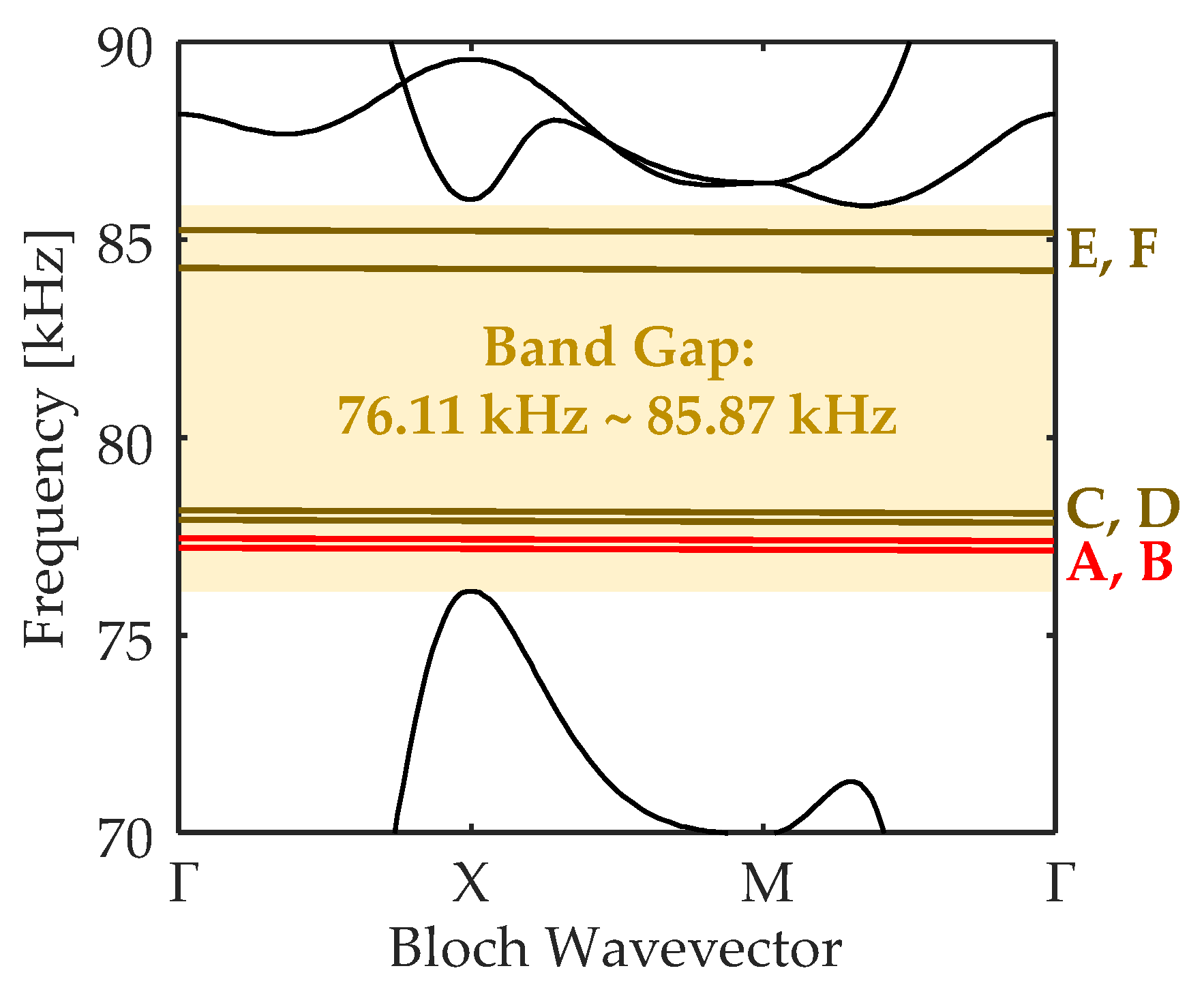
Band–structure analysis in waves, which is analogous to modal analysis in vibrations, plays a significant role in (1) specifying dispersion relations (eigenfrequencies in an eigenvalue problem) of the PnC and (2) visualizing mode shapes (eigenvectors in an eigenvalue problem) of the PnC at given frequencies [47,48]. Figure 2 depicts the dispersion results of the PnC shown in Figure 1 [49,50]. The x-axis stands for the Bloch wavevectors that belong to the first Brillouin zone (Γ→X→M→Γ) and the y-axis stands for the eigenfrequency, ranging from 70 kHz to 90 kHz. In dispersion curves, the PBG refers to a frequency range where wavevectors in all directions do not correspond to all polarized wavemodes (e.g., symmetric and antisymmetric Lamb waves and shear-horizontal waves in a thin plate) [51]. We confirm that the PBG, highlighted in a light orange box, lies in a range from 76.11 kHz to 85.87 kHz. It is well known that the PBG represents non-real complex wavevectors [52]; thus, the PnC undergoes exponentially decreasing evanescent waves [53].
Before providing a description of the defect band results, it is necessary to summarize the physical meanings of two electrical boundary conditions (i.e., namely short- and open-circuit conditions) of the defect bands. Under the short-circuit condition, where an external electrical resistance connected to one piezoelectric patch is close to zero, the patch and aluminum lattice are only mechanically coupled. On the other hand, under the open-circuit condition, where the electrical resistance becomes very large, the piezoelectric effects make the patch and aluminum lattice electromechanically coupled and maximally generate output voltage.
Under the short-circuit condition of the piezoelectric patches, Figure 2 shows that six defect bands, colored in solid red or brown lines, emerge within the PBG. The corresponding frequency of each defect band, labeled from A to F is summarized as follows: 77.77 kHz (A), 77.84 kHz (B), 78.29 kHz (C), 78.40 kHz (D), 84.30 kHz (E), and 85.20 kHz (F). Recall that the instantaneous slope (=Δangular frequency/Δwavenumber) in the band structures means a group velocity within a PnC. Therefore, zero energy transport velocity of defect bands indicates that the incident elastic waves are trapped within the PnC, especially within the defect [54].
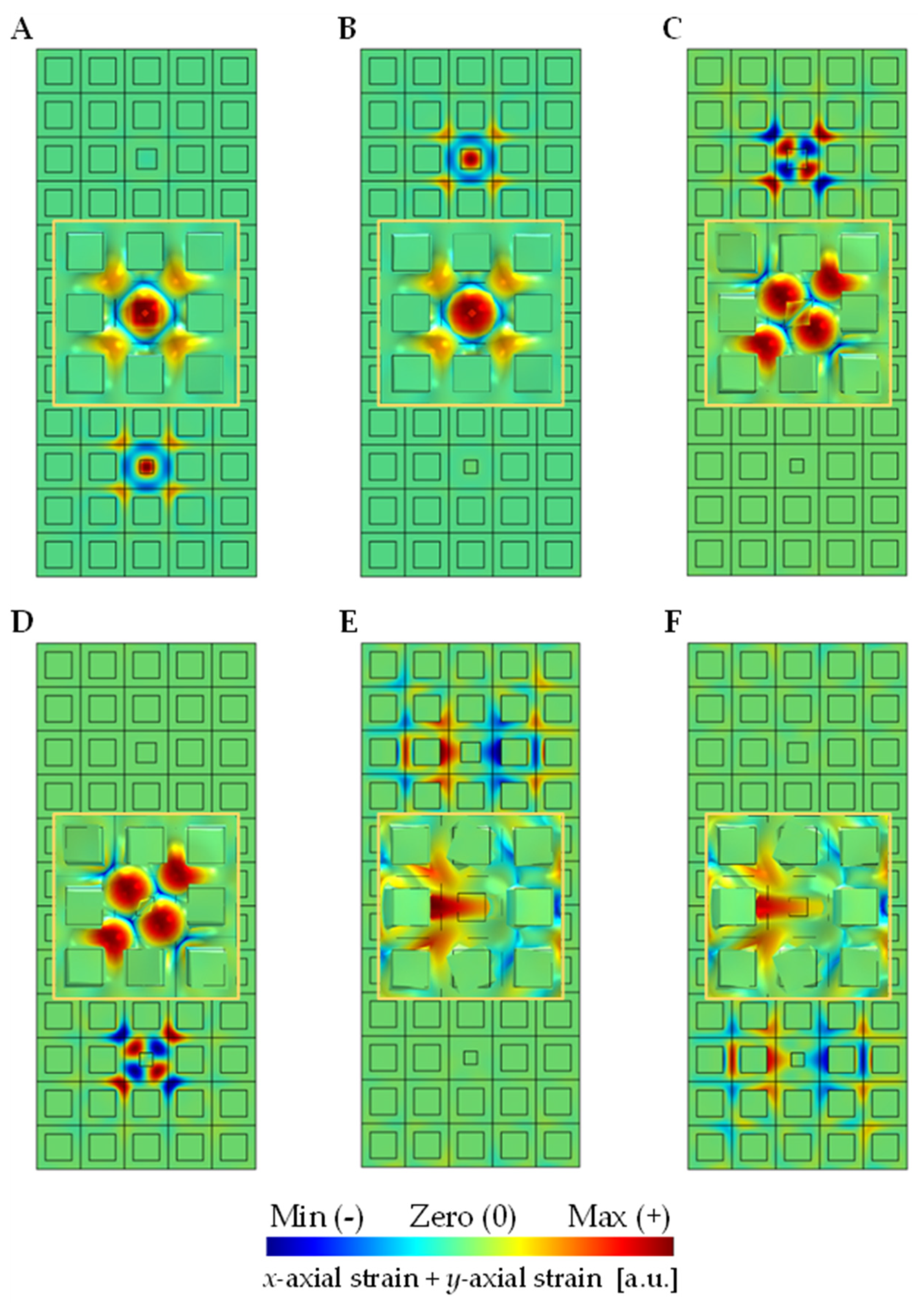
Figure 3 presents snapshots of the defect mode shapes of the PnC with the differently configured double defects at each defect band found in Figure 2. In previous studies, the defect mode shape has been defined in various ways, such as by the displacement [55], velocity [56], strain [57], and stress (pressure) fields [58] of PnCs. From the perspective of PEH, it is meaningful to analyze the strain field, since the constitutive equations of linear piezoelectricity state that the electric field generated in the piezoelectric materials is proportional to the mechanical strain [59,60,61]. Therefore, in this study, the defect mode shape refers to the normalized strain field of the PnC. In particular, in the case of bending motions (e.g., A0 Lamb waves) of a thin piezoelectric patch, since the sum of the x- and y-axial strains is dominantly involved in electromechanical coupling [62], Figure 3 depicts these strain fields without deformed configurations. Labels from A to F are marked on the top left of each figure. An enlarged view of the deformed configurations near the defect is presented in the middle of each figure. In Figure 2 and Figure 3, there are three crucial points to be emphasized, as follows.
First, the defect mode shapes of A, D, and F show that most elastic wave energy is confined in the vicinity of only the defect located at (3, 3). In contrast, the remaining defect mode shapes of B, C, and E feature the energy-localized behaviors in the vicinity of only the defect situated at (3, 10). At the same time, through comparison of the pairs of (A-B), (C-D), and (E-F), it should be borne in mind that the energy-localized defect mode shapes within each defect are similar. The demonstration of these results can be offered in the context of the superposition of (1) the decoupling characteristic between the double defects and (2) the different physical quantities (i.e., inertia and stiffness) of the piezoelectric patches. When one defect is imposed at a location sufficiently distant from the other defect, the defects are not aware of the existence of each other; thus, each defect behaves as a single independent defect. Therefore, by supposing an identical configuration of the defects, as shown in [39], the elastic wave energy will be localized to each defect at the same defect band frequency that corresponds to a single defect. Here, as specified in [32], we need to keep in mind that defect bands can be shifted, depending on the inertia and stiffness of the piezoelectric patches inside the defect. To support this interpretation, under the same unit cells shown in Figure 1, Appendix A provides a description of how the defect band frequencies in the single-defect case vary with the length of the piezoelectric patch. This implies that—induced by the different geometric dimensions of the piezoelectric patches—independently vibrating defects will display separated different defect bands.
Second, following the previous research [32,40], we delineate the selection of the target defect mode shape by delving into the increasing amount of each defect band frequency when we switch the electric boundary from short-circuit to open-circuit conditions. In Figure 3, the observation of the sign of strain fields within each defect confirms that strain nodal lines (the colors close to green) are formed inside the piezoelectric patches for all defect mode shapes, other than those of A and B. If a piezoelectric patch undergoes both elongation and compression (in other words, different signs of strains), undesirable electric charge cancellation occurs [63,64]. This reduces the degree of electromechanical coupling and seriously worsens the output voltage. Hence, we can qualitatively assert that the defect modes of A and B are suitable for highly dense PEH. To support this interpretation by examining quantitative results, under the open-circuit condition, each defect band frequency is calculated as follows: 78.28 kHz (A’), 78.51 kHz (B’), 78.29 kHz (C’), 78.40 kHz (D’), 84.30 kHz (E’), and 85.20 kHz (F’). The prime, which is the superscript of the labels, refers to a band that corresponds to each defect mode shape in Figure 3, among the defect bands obtained under the open-circuit condition. It is worthwhile to note that the defect bands of A’ and B’ are shifted by 510 Hz and 670 Hz, respectively, as compared with the defect bands of A and B. On the other hand, no shift occurs in the remaining defect bands; this infers that complete voltage cancellation takes place in the piezoelectric patches due to the antisymmetric strain fields in piezoelectric patches. Therefore, it is desirable to select the defect mode shapes of A and B, which are called monopole-like defect mode shapes in this study; the corresponding defect bands are highlighted in red in Figure 2. Note that these defect mode shapes are primarily polarized out-of-plane; thereby, they fit our situation in consideration of A0 Lamb waves.
Last, as key findings that are set apart from the conventionally graded PnC with decoupled double defects [39], the degree of electromechanical coupling in each defect is distinguished, since differently configured patches are taken into account. The difference between the frequencies corresponding to the defect bands of A and B under the short-circuit condition is 70 Hz; on the other hand, the difference between those of A’ and B’ under the open-circuit condition is much larger, at 230 Hz. For the bending motions, the literature in [62] presented that the degree of electromechanical coupling was linear to the definite integral of the summation of the x- and y-axial strains over the piezoelectric patch. Therefore, the larger the square piezoelectric patch before voltage cancellation occurs, the more strengthened the electromechanical coupling and the more shifted the defect band frequencies. To support this interpretation, in the single-defect case with the same unit cells shown in Figure 1, Appendix A provides results of how the shift pattern of the defect band frequency corresponding to the monopole-like defect mode shape varies with the length of the piezoelectric patch. These results imply that a proposed PnC concept with decoupled double defects of a different configuration must be designed in keeping with the fact that the shift patterns of defect band frequencies of each defect are different, when tailoring the separated defect band frequencies for broadband PEH purposes.
In summary, if a PnC with differently configured double defects is exposed to elastic waves, dramatically amplified output performance of the PEH can be expected near 78.28 kHz and 78.51 kHz under the open-circuit condition, thanks to independent monopole-shaped energy-localized behaviors. Therefore, it can be expected that the superimposition of these properties enables the localization of A0 Lamb waves propagating over a wide range of frequencies and broadens the bandwidth for PEH performance.
3.2. Piezoelectric Energy Harvesting Performance Analysis
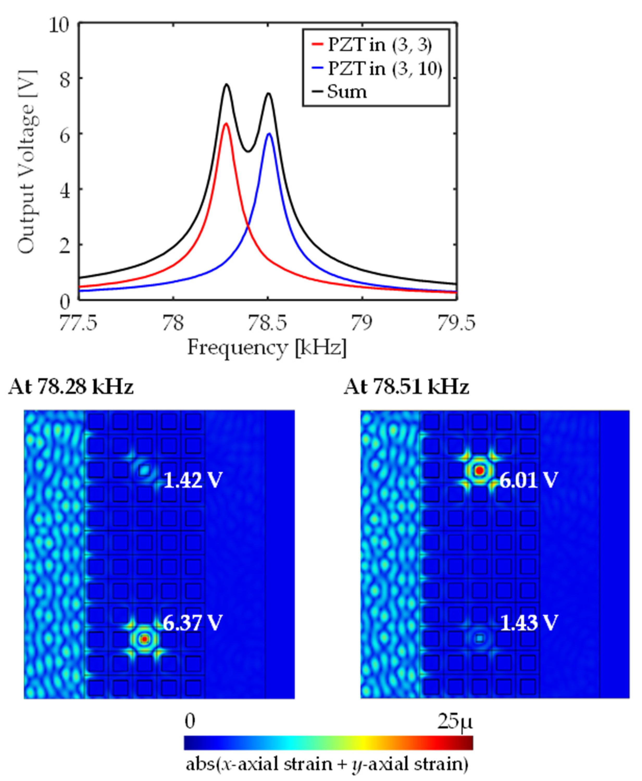
The output performance of PEH is thoroughly evaluated through time–harmonic analysis using FRFs for both (1) output voltage under the open-circuit condition and (2) output electric power across the power-optimal external electric resistances. The top graph in Figure 4 shows output voltage results under the open-circuit condition. Solid red and blue lines stand for the output electric responses calculated at the piezoelectric patches deployed at (3, 3) and (3, 10), respectively. The maximum output voltage is obtained in each patch as: 6.37 V at 78.28 kHz at (3, 3) and 6.01 V at 78.51 kHz at (3, 10). Note that these peak frequencies are equal to the defect-band frequencies of A’ and B’. As a reference, in the case without the PnC, the patches at (3, 3) and (3, 10) show output voltages of 0.27 V at 78.28 kHz and 0.21 V at 78.51 kHz, respectively. The existence of the double-defects-induced PnCs thus enables amplification of the output voltage to be 23.59 and 28.61 times larger at each frequency, respectively. The bottom part in Figure 4 illustrates the absolute strain fields of the operating deflection shapes of the overall structure at the peak frequencies of 78.28 kHz and 78.51 kHz, when the incident elastic waves enter from the left end of each figure. The elastic waves are dominantly localized and amplified in the vicinity of the defects located at (3, 3) and (3, 10) for each frequency, respectively. Here, unlike the results shown in Figure 3, it can be also seen that monopole-like energy-localized behaviors vaguely appear in the other patch at each peak frequency. These differences can be conceptually understood as the differences between normal mode shapes (modal analysis) and operating deflection shapes (time-harmonic analysis) in the vibrations.
In Figure 4, two important messages need to be emphasized. First, it is observed that only one peak appears in each FRF and the peak frequency of each patch is different. From these two separated FRFs of the patches, it can be concluded that (1) the double defects are well decoupled, and (2) independently tailoring each FRF comes into effect due to differently patterned patches. In earlier studies of PnCs with closely arranged and identically configured double defects [38,65], the synchronous energy-localized behaviors (i.e., in-phase and out-of-phase defect mode shapes) are displayed inside both defects at two different frequencies. Therefore, two peak frequencies in output electric response FRFs for each defect should be observed. Second, after transforming an AC voltage signal into a DC voltage signal via the AC-DC converter, the output voltages generated by each patch can be summed. The solid black line stands for the summation results; the summed voltages at 78.28 kHz and 78.51 kHz are 7.79 V and 7.44 V, respectively. Therefore, it can be found that the proposed PnC design has the ability to achieve broadband elastic wave energy localization and harvesting with the help of the superposition of decoupling and different configuration characteristics.
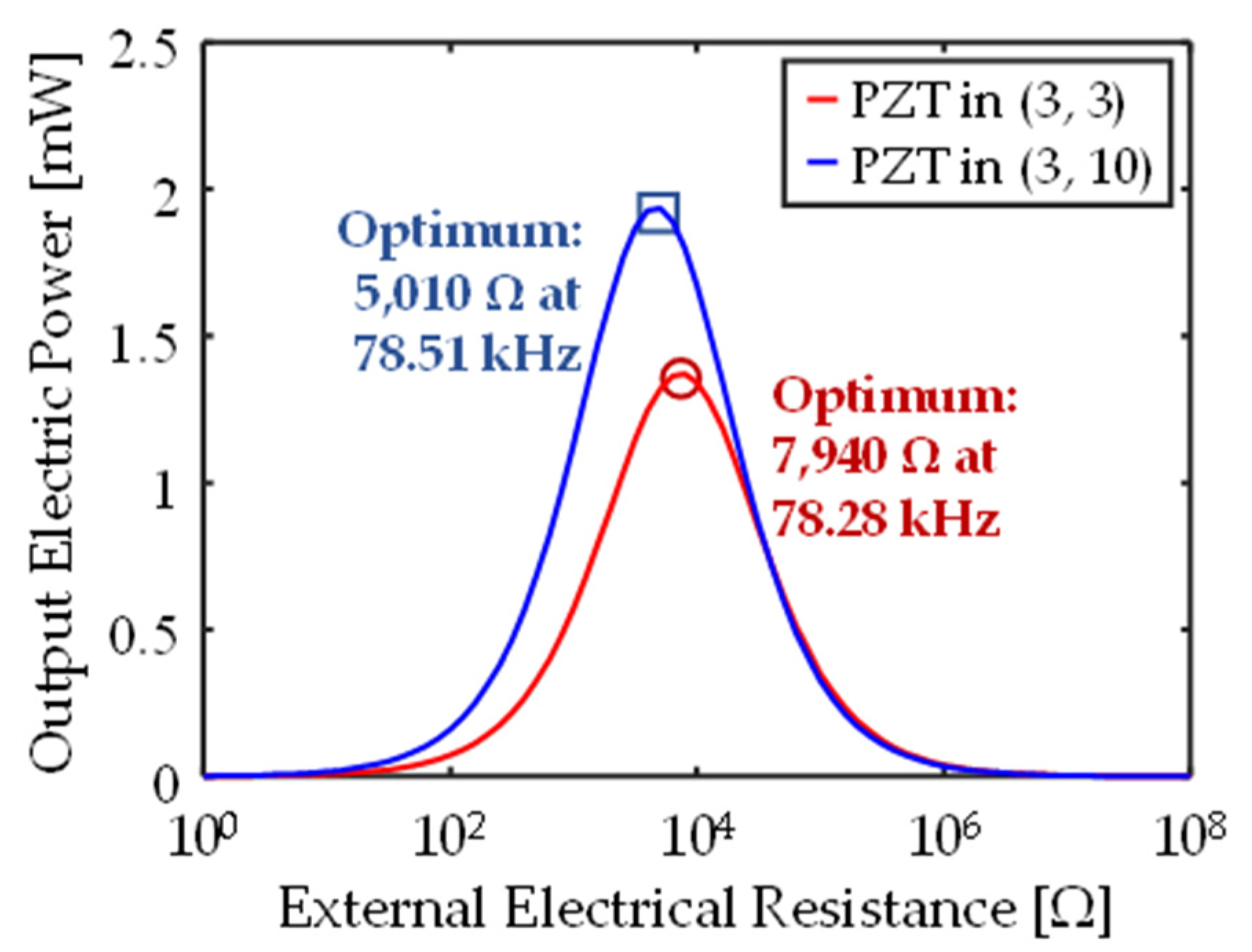
In terms of output electric power, one crucial issue that should be addressed is to minimize the electrical impedance mismatching between one piezoelectric patch and external electrical resistance in connected electric circuits. In this study, following Ohm’s law, output electric power can be given by Voltage2/Resistance. When the resistance converges to zero (i.e., short-circuit condition), the voltage will approach zero due to nearly zero electromechanical coupling, thus resulting in zero electric power. In contrast, if the resistance becomes very large (close to the open-circuit condition), output electric power will also converge to zero. Hence, output electric power, a function of the electrical resistance, will be convex upward [66,67]. In this study, a resistance that can maximize the output electric power at the peak frequency found under the open-circuit condition is called a power-optimal external electrical resistance. To numerically find the power-optimal external electrical resistance, Figure 5 presents output electric power results with respect to the external electrical resistance, ranging from 0 Ω to 100 MΩ. Solid red and blue lines stand for the results of each patch at (3, 3) and (3, 10) at peak frequencies of 78.28 kHz and 78.51 kHz, respectively. As highlighted with the dark-red circle and dark-blue square in Figure 5, the power-optimal external electrical resistances are calculated as (1) 7940 Ω for the patch at (3, 3) at 78.28 kHz and (2) 5010 Ω for the patch at (3, 10) at 78.51 kHz, respectively.
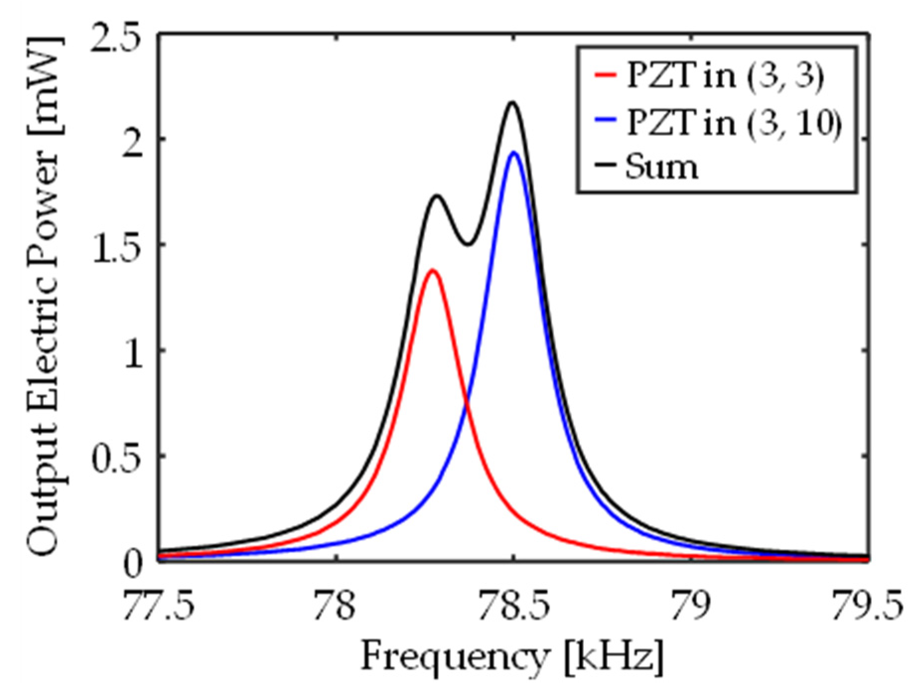
Figure 6 shows the results of output electric power FRFs when each patch at (3, 3) and (3, 10) is connected with the power-optimal external electrical resistances of 7940 Ω and 5010 Ω, respectively. Solid red and blue lines stand for the output electric responses calculated at the patches deployed at (3, 3) and (3, 10), respectively. The maximum output electric power of each patch is obtained as: 1.39 mW at 78.28 kHz at (3, 3) and 1.94 mW at 78.51 kHz at (3, 10). Thanks to AC-DC converters, the output electric power generated by each patch can be summed, as plotted by the solid black line; the summed output electric power at 78.28 kHz and 78.51 kHz is 1.73 mW and 2.17 mW, respectively. Thus, we can conclude that the proposed design concept of a PnC with differently configured and decoupled double defects enables a broadening of the bandwidth for both output voltage and electric power; more than doubling the results of the prior single defect approach.
In summary, a conceptual way to implement broadband PEH is to sum the independent output performances of separated defects after converting AC signals into DC signals. When designing the proposed PnC concept for broadband PEH purposes, it should be emphasized that the peak frequency and bandwidth (in other words, Q factor) of the output electrical response FRFs obtained from a PnC with a single defect must be taken into account. The reasons can be summarized as follows. One is about the difference between the peak frequencies when a Q-factor is given. If the difference is large, the summed PEH performance will drop sharply between the two frequencies; on the other hand, if the difference is small, the desirable broadband characteristics can be worsened. The other is about the dependence on the Q-factor. When the Q-factor is small, the overall output performance of PEH can be broader with proper spacing between the peak frequencies. However, a trade-off relationship exists in which the absolute values of output voltage and electric power at each peak frequency become smaller. Therefore, designing defect band frequencies and selecting Q-factors of the double defects in consideration of the existing FRF characteristics for a single defect is essential for broadband elastic wave energy localization and harvesting.
4. Conclusions
This study newly proposed a PnC with differently configured double defects for broadband elastic wave energy localization and harvesting. The unit cell under consideration was an aluminum square lattice, to which an aluminum square pillar was attached. A PnC was built by arranging 5 × 12 unit cells along the x- and y- directions. At the same time, double defects were created in the manner where differently configured piezoelectric patches with the lengths of 6 mm and 9mm were attached to square lattices at the locations of (3, 3) and (3, 10) for power generation, rather than attaching the pillars. Through preliminary studies, it was found that these locations were distant enough to guarantee decoupling characteristics; thus, the defects behaved as single independent defects. Furthermore, since the generated defect bands varied with the inertia and stiffness of the piezoelectric patch inside the defect, the proposed PnC design allowed separate manipulation of defect band frequencies by differentiating geometric dimensions of each piezoelectric patch. As a result, at each defect band frequency of 78.28 kHz and 78.51 kHz under the open-circuit condition, each defect at (3, 3) and (3, 10) represented the monopole-shaped energy-localized behavior, respectively. With the help of these properties, under both the open-circuit condition and power-optimal external electrical resistances, each piezoelectric patch showed independent FRFs for output performance of PEH whose peak frequencies were different. By using AC-DC converters, the output electrical responses (i.e., output voltage and electric power) obtained by each patch could be summed, thus successfully more than doubling the bandwidth of the output voltage and electric power. In this context, we anticipate that the introduction of differently patterned multiple (more than double) defects with a greater number of unit cells enables further broadening the bandwidth by bringing multiple defect band frequencies closer. Here, when designing the proposed PnC concept, two points that should be borne in mind are outlined as follows. First, when switching the electric boundary from short-circuit to open-circuit conditions, the shift patterns of the defect band frequencies for each piezoelectric patch are different, depending on their geometry. Second, the peak frequency and bandwidth of the output electrical response FRF obtained from a PnC with a single defect must be considered in order to design an adequate difference between the peak frequencies and select a proper Q-factor. Note that this work considered incident plane waves. If one may use a point source that is positioned close to the PnC or within the PnC, there are possibilities that the considerable difference between the PEH performances obtained at each peak frequency can worsen the broadband characteristics, depending on the source location. This is the limitation of this work.
In future works, two topics are under consideration as follows. First, it should be stated that lots of mechanical systems (e.g., railway [68]) with which a PnC-based PEH system may be equipped are exposed to dynamic thermal loading (e.g., external temperature environment and Joule heating during operation). Since the mechanical strain and stress in both the host plate and piezoelectric materials can change due to the temperature effects, not only the absolute output electric power [69], but also the broadband characteristics in the PnC-inspired PEH system can be affected by the thermal loading. Therefore, this issue highlights one research need of quantification of temperature effects on output performance of the PEH of the proposed PnC design. Second, the piezoelectric patches can be partially debonded from a host plate due to impact loading, bonding defects, environmental effects, fatigue loading, or high free-edge stresses [70,71]. As debonding increases, the effective area of the surface-bonded piezoelectric layer could be decreased, resulting in a reduction in the output voltage. Therefore, this issue highlights one research need of performance degradation assessment of a PnC-inspired PEH system in the presence of partial debonding.
Author Contributions
Conceptualization, S.-H.J.; methodology, S.-H.J. and B.D.Y.; formal analysis, S.-H.J. and B.D.Y.; writing—original draft preparation, S.-H.J. and B.D.Y.; writing—review & editing, S.-H.J. and B.D.Y.; supervision, B.D.Y.; funding acquisition, B.D.Y. All authors have read and agreed to the published version of the manuscript.
Funding
This work was supported by the National Research Foundation of Korea (NRF) grant funded by the Korea Government (MSIT) (No. 2020R1A2C3003644).
Conflicts of Interest
The authors declare no conflict of interest.
Appendix A. Effects of the Length of a Piezoelectric Patch Attached to a Single Defect on Defect Band Frequencies
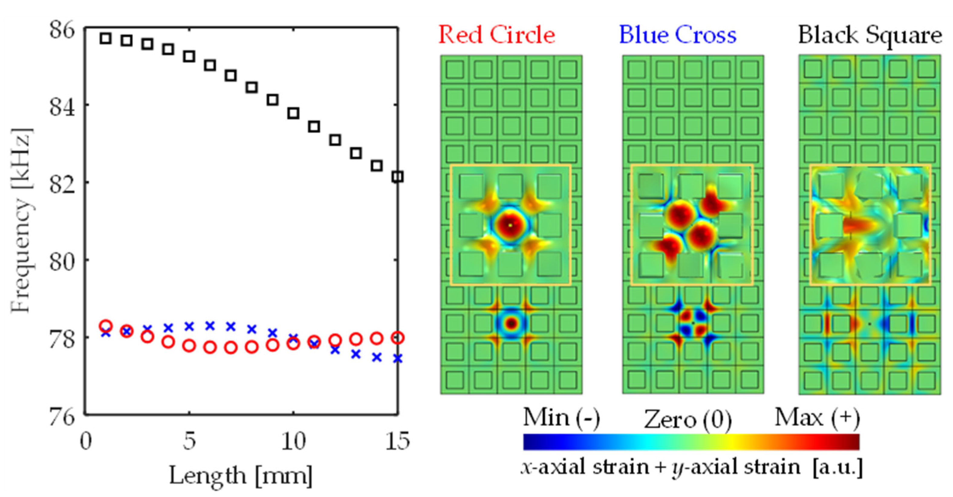
Band–structure analysis is performed for a PnC with a single defect introduced at the location of (3, 3) under the short-circuit condition. The left graph in Figure A1 depicts how three defect bands generated in the PBG vary with the length of the piezoelectric patch, ranging from 1 mm to 15 mm. Dots with red circles, blue crosses, and black squares indicate the defect bands that correspond to the pairs of (A-B), (C-D), and (D-F), which are found in both Figure 2 and Figure 3, respectively. For example, in the case of the length of 1 mm, the top view of defect mode shapes of the PnC at each defect band frequency is visualized in the right part of Figure A1. It can be seen that the defect band frequency corresponding to the red circles (blue crosses) decreases (increases) until it reaches a particular length of 6 mm and then increases (decreases). On the other hand, the defect band frequency corresponding to the black squares monotonically decreases. In summary, the key message is that the defect band frequencies significantly depend on the length of the piezoelectric patch, due to the variation of its inertia and stiffness.
Figure A1.
Relationships between the length of the piezoelectric patch and defect band frequencies for the PnC with the single defect.
Figure A1.
Relationships between the length of the piezoelectric patch and defect band frequencies for the PnC with the single defect.

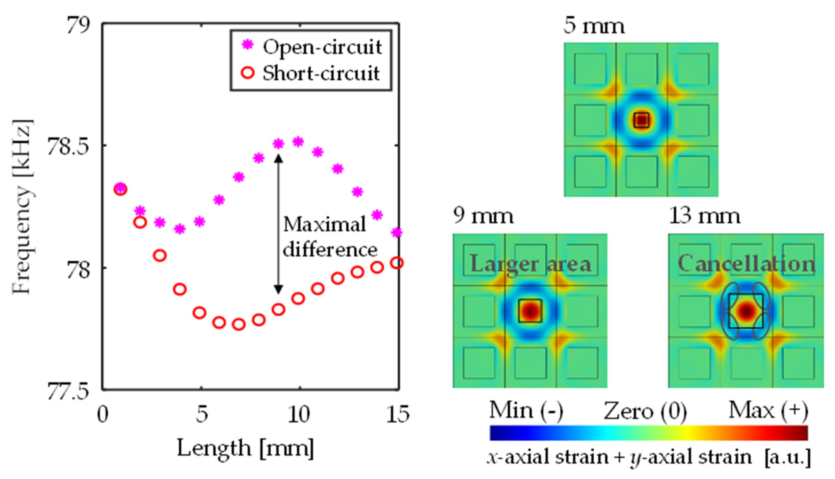
Figure A2.
Relationships between the length of the piezoelectric patch and the shift pattern of the defect band frequency that corresponds to the monopole-like defect mode shape for the PnC with the single defect when the electrical boundary is switched from short-circuit to open-circuit conditions.

Next, when the electrical boundary is switched from the short-circuit to open-circuit conditions, the left graph in Figure A2 represents how the defect band frequency that corresponds to the monopole-like defect mode shape (red circles in Figure A1) varies with the length of the piezoelectric patch. Dots with red circles and magenta stars indicate the results under short-circuit and open-circuit conditions, respectively. As examples of the lengths of 5 mm, 9 mm, and 13 mm, the enlarged top view of the defect mode shapes near the defect at each defect band frequency is visualized in the right part of Figure A2. The key findings are that the difference between the two defect band frequencies at a given length increases until the particular length of 9 mm, and then the difference decreases. Referring to the analytical model of a piezoelectric energy harvester proposed by Yoon et al. [62], the amount of the defect band frequency shift from the short-circuit to open-circuit condition can be explained by:
where ωshort and ωopen are angular frequencies of a defect band under the short-circuit and open-circuit conditions, respectively. Cp and ζ are the capacitance of a piezoelectric patch and structural damping ratio, respectively. θ stands for the electromechanical coupling factor, which is in linear relationships with the strain distribution of the piezoelectric patch as:
where Sp is the attachment area of the patch. εxx and εyy are the x-axial and y-axial normal strains, respectively. It can be found that the difference between the defect band frequencies under the short-circuit to open-circuit conditions increases as the degree of electromechanical coupling increases. Therefore, the increasing and decreasing trends can be elucidated by the increasing area and electric charge cancellation, respectively. In summary, the defect band frequency depends on the length of the piezoelectric patch, due to the variation of its electromechanical coupling.
References
- Ma, K.; Tan, T.; Yan, Z.; Liu, F.; Liao, W.-H.; Zhang, W. Metamaterial and Helmholtz coupled resonator for high-density acoustic energy harvesting. Nano Energy 2021, 82, 105693. [Google Scholar] [CrossRef]
- Shin, Y.C.; Yoon, H.; Jo, S.-H.; Choi, W.; Park, C.-S.; Kim, M.; Youn, B.D. Phononic band gap of a quarter-wave stack for enhanced piezoelectric energy harvesting. Int. J. Mech. Sci. 2020, 192, 106003. [Google Scholar]
- Tan, T.; Yan, Z.; Zou, H.; Ma, K.; Liu, F.; Zhao, L.; Peng, Z.; Zhang, W. Renewable energy harvesting and absorbing via multi-scale metamaterial systems for Internet of things. Appl. Energy 2019, 254, 113717. [Google Scholar] [CrossRef]
- Tol, S.; Degertekin, F.; Erturk, A. Phononic crystal Luneburg lens for omnidirectional elastic wave focusing and energy harvesting. Appl. Phys. Lett. 2017, 111, 013503. [Google Scholar] [CrossRef]
- Chen, Z.; Guo, B.; Yang, Y.; Cheng, C. Metamaterials-based enhanced energy harvesting: A review. Phys. B Condens. Matter 2014, 438, 1–8. [Google Scholar] [CrossRef]
- Zou, H.-X.; Zhao, L.-C.; Gao, Q.-H.; Zuo, L.; Liu, F.-R.; Tan, T.; Wei, K.-X.; Zhang, W.-M. Mechanical modulations for enhancing energy harvesting: Principles, methods and applications. Appl. Energy 2019, 255, 113871. [Google Scholar] [CrossRef]
- Al-Yafeai, D.; Darabseh, T.; Mourad, A.-H.I. A state-of-the-art review of car suspension-based piezoelectric energy harvesting systems. Energies 2020, 13, 2336. [Google Scholar] [CrossRef]
- Wang, J.; Geng, L.; Ding, L.; Zhu, H.; Yurchenko, D. The state-of-the-art review on energy harvesting from flow-induced vibrations. Appl. Energy 2020, 267, 114902. [Google Scholar] [CrossRef]
- Wu, N.; Bao, B.; Wang, Q. Review on engineering structural designs for efficient piezoelectric energy harvesting to obtain high power output. Eng. Struct. 2021, 235, 112068. [Google Scholar] [CrossRef]
- Yan, Z.; Abdelkefi, A.; Hajj, M.R. Piezoelectric energy harvesting from hybrid vibrations. Smart Mater. Struct. 2014, 23, 025026. [Google Scholar] [CrossRef]
- Tan, T.; Yan, Z.; Huang, W. Broadband design of hybrid piezoelectric energy harvester. Int. J. Mech. Sci. 2017, 131, 516–526. [Google Scholar] [CrossRef]
- Yan, Z.; Hajj, M.R. Energy harvesting from an autoparametric vibration absorber. Smart Mater. Struct. 2015, 24, 115012. [Google Scholar] [CrossRef]
- Cui, J.; Yoon, H.; Youn, B.D. An omnidirectional biomechanical energy harvesting (OBEH) sidewalk block for a self-generative power grid in a smart city. Int. J. Pr. Eng. Manuf. Green Technol. 2018, 5, 507–517. [Google Scholar] [CrossRef]
- Yoon, H.; Kim, M.; Park, C.-S.; Youn, B.D. Time-varying output performances of piezoelectric vibration energy harvesting under nonstationary random vibrations. Smart Mater. Struct. 2017, 27, 015004. [Google Scholar] [CrossRef]
- Liu, J.; Guo, H.; Wang, T. A review of acoustic metamaterials and phononic crystals. Crystals 2020, 10, 305. [Google Scholar] [CrossRef]
- Li, Y.F.; Meng, F.; Zhou, S.; Lu, M.-H.; Huang, X. Broadband all-angle negative refraction by optimized phononic crystals. Sci. Rep. 2017, 7, 7445. [Google Scholar] [CrossRef]
- Darabi, A.; Leamy, M.J. Analysis and experimental validation of an optimized gradient-index phononic-crystal lens. Phys. Rev. Appl. 2018, 10, 024045. [Google Scholar] [CrossRef]
- Dai, H.; Liu, T.; Jiao, J.; Xia, B.; Yu, D. Double Dirac cone in two-dimensional phononic crystals beyond circular cells. J. Appl. Phys. 2017, 121, 135105. [Google Scholar] [CrossRef]
- Jo, S.-H.; Xia, Y.; Moura, A.G.; Yoon, H.; Shin, Y.C.; Erturk, A.; Youn, B.D. Experimentally validated broadband self-collimation of elastic waves. Int. J. Mech. Sci. 2021, 192, 106131. [Google Scholar] [CrossRef]
- Guo, Y.; Li, L.; Chuang, K.-C. Analysis of bending waves in phononic crystal beams with defects. Crystals 2018, 8, 21. [Google Scholar] [CrossRef] [Green Version]
- Sigalas, M. Defect states of acoustic waves in a two-dimensional lattice of solid cylinders. J. Appl. Phys. 1998, 84, 3026–3030. [Google Scholar] [CrossRef]
- Zhang, L.-Y.; Yin, X.; Yang, J.; Li, A.; Xu, G.-K. Multilevel structural defects-induced elastic wave tunability and localization of a tensegrity metamaterial. Compos. Sci. Technol. 2021, 207, 108740. [Google Scholar] [CrossRef]
- Li, F.; Wang, Y. Elastic wave propagation and localization in band gap materials: A review. Sci. China Phys. Mech. 2012, 55, 1734–1746. [Google Scholar] [CrossRef]
- Miranda, E.; Aranas, C.; Rodrigues, S.; Silva, H.; Reis, G.; Paiva, A.; Dos Santos, J. Dispersion diagram of trigonal piezoelectric phononic structures with Langasite inclusions. Crystals 2021, 11, 491. [Google Scholar] [CrossRef]
- Wang, Y.-F.; Wang, Y.-S. Multiple wide complete bandgaps of two-dimensional phononic crystal slabs with cross-like holes. J. Sound Vib. 2013, 332, 2019–2037. [Google Scholar] [CrossRef]
- Lee, I.K.; Kim, Y.J.; Oh, J.H.; Kim, Y.Y. One-dimensional broadband phononic crystal filter with unit cells made of two non-uniform impedance-mirrored elements. AIP Adv. 2013, 3, 022105. [Google Scholar] [CrossRef] [Green Version]
- Wang, P.; Chen, T.-N.; Yu, K.-P.; Wang, X.-P. Lamb wave band gaps in a double-sided phononic plate. J. Appl. Phys. 2013, 113, 053509. [Google Scholar] [CrossRef]
- Yao, Z.-J.; Yu, G.-L.; Wang, Y.-S.; Shi, Z.-F. Propagation of bending waves in phononic crystal thin plates with a point defect. Int. J. Solids Struct. 2009, 46, 2571–2576. [Google Scholar] [CrossRef] [Green Version]
- Li, Y.; Zhu, L.; Chen, T.; Ye, Q. Elastic wave confinement and absorption in a dissipative metamaterial. Indian J. Pure Appl. Phys. 2018, 56, 158–163. [Google Scholar]
- Park, C.-S.; Shin, Y.C.; Jo, S.-H.; Yoon, H.; Choi, W.; Youn, B.D.; Kim, M. Two-dimensional octagonal phononic crystals for highly dense piezoelectric energy harvesting. Nano Energy 2019, 57, 327–337. [Google Scholar] [CrossRef]
- Geng, Q.; Cai, T.; Li, Y. Flexural wave manipulation and energy harvesting characteristics of a defect phononic crystal beam with thermal effects. J. Appl. Phys. 2019, 125, 035103. [Google Scholar] [CrossRef]
- Jo, S.-H.; Yoon, H.; Shin, Y.C.; Youn, B.D. An analytical model of a phononic crystal with a piezoelectric defect for energy harvesting using an electroelastically coupled transfer matrix. Int. J. Mech. Sci. 2021, 193, 106160. [Google Scholar] [CrossRef]
- Lv, X.-F.; Fang, X.; Zhang, Z.-Q.; Huang, Z.-L.; Chuang, K.-C. Highly localized and efficient energy harvesting in a phononic crystal beam: Defect placement and experimental validation. Crystals 2019, 9, 391. [Google Scholar] [CrossRef] [Green Version]
- Deng, T.; Zhang, S.; Gao, Y. A magnetic-dependent vibration energy harvester based on the tunable point defect in 2D magneto-elastic phononic crystals. Crystals 2019, 9, 261. [Google Scholar] [CrossRef] [Green Version]
- Lee, T.-G.; Jo, S.-H.; Seung, H.M.; Kim, S.-W.; Kim, E.-J.; Youn, B.D.; Nahm, S.; Kim, M. Enhanced energy transfer and conversion for high performance phononic crystal-assisted elastic wave energy harvesting. Nano Energy 2020, 78, 105226. [Google Scholar] [CrossRef]
- Ma, T.-X.; Fan, Q.-S.; Li, Z.-Y.; Zhang, C.; Wang, Y.-S. Flexural wave energy harvesting by multi-mode elastic metamaterial cavities. Extrem. Mech. Lett. 2020, 41, 101073. [Google Scholar] [CrossRef]
- Lv, H.; Tian, X.; Wang, M.Y.; Li, D. Vibration energy harvesting using a phononic crystal with point defect states. Appl. Phys. Lett. 2013, 102, 034103. [Google Scholar] [CrossRef] [Green Version]
- Jo, S.-H.; Yoon, H.; Shin, Y.C.; Kim, M.; Youn, B.D. Elastic wave localization and harvesting using double defect modes of a phononic crystal. J. Appl. Phys. 2020, 127, 164901. [Google Scholar] [CrossRef] [Green Version]
- Jo, S.-H.; Yoon, H.; Shin, Y.C.; Youn, B.D. A graded phononic crystal with decoupled double defects for broadband energy localization. Int. J. Mech. Sci. 2020, 183, 105833. [Google Scholar] [CrossRef]
- Jo, S.-H.; Yoon, H.; Shin, Y.C.; Choi, W.; Park, C.-S.; Kim, M.; Youn, B.D. Designing a phononic crystal with a defect for energy localization and harvesting: Supercell size and defect location. Int. J. Mech. Sci. 2020, 179, 105670. [Google Scholar] [CrossRef]
- Miniaci, M.; Gliozzi, A.S.; Morvan, B.; Krushynska, A.; Bosia, F.; Scalerandi, M.; Pugno, N.M. Proof of concept for an ultrasensitive technique to detect and localize sources of elastic nonlinearity using phononic crystals. Phys. Rev. Lett. 2017, 118, 214301. [Google Scholar] [CrossRef] [Green Version]
- Erturk, A.; Inman, D.J. Piezoelectric Energy Harvesting; John Wiley & Sons: Hoboken, NJ, USA, 2011. [Google Scholar]
- Hyun, J.; Choi, W.; Kim, M. Gradient-index phononic crystals for highly dense flexural energy harvesting. Appl. Phys. Lett. 2019, 115, 173901. [Google Scholar] [CrossRef]
- Tol, S.; Degertekin, F.; Erturk, A. 3D-printed phononic crystal lens for elastic wave focusing and energy harvesting. Addit. Manuf. 2019, 29, 100780. [Google Scholar] [CrossRef]
- Wang, W.-C.; Wu, L.-Y.; Chen, L.-W.; Liu, C.-M. Acoustic energy harvesting by piezoelectric curved beams in the cavity of a sonic crystal. Smart Mater. Struct. 2010, 19, 045016. [Google Scholar] [CrossRef]
- Sun, K.H.; Kim, J.E.; Kim, J.; Song, K. Sound energy harvesting using a doubly coiled-up acoustic metamaterial cavity. Smart Mater. Struct. 2017, 26, 075011. [Google Scholar] [CrossRef]
- Romero-García, V.; Sánchez-Pérez, J.; Garcia-Raffi, L. Evanescent modes in sonic crystals: Complex dispersion relation and supercell approximation. J. Appl. Phys. 2010, 108, 044907. [Google Scholar] [CrossRef]
- Sangster, M.; Hussain, A. The supercell method for calculating responses in defective lattices. Physica B+C 1985, 131, 119–125. [Google Scholar] [CrossRef]
- Yi, G.; Shin, Y.C.; Yoon, H.; Jo, S.-H.; Youn, B.D. Topology optimization for phononic band gap maximization considering a target driving frequency. JMST Adv. 2019, 1, 153–159. [Google Scholar] [CrossRef] [Green Version]
- Miranda, E.J.P.D., Jr.; Santos, J.M.C.D. Complete band gaps in nano-piezoelectric phononic crystals. Mater. Res. 2017, 20, 15–38. [Google Scholar] [CrossRef] [Green Version]
- Kafesaki, M.; Sigalas, M.; Economou, E. Elastic wave band gaps in 3-D periodic polymer matrix composites. Solid State Commun. 1995, 96, 285–289. [Google Scholar] [CrossRef] [Green Version]
- Bavencoffe, M.; Morvan, B.; Hladky-Hennion, A.-C.; Izbicki, J.-L. Experimental and numerical study of evanescent waves in the mini stopband of a 1D phononic crystal. Ultrasonics 2013, 53, 313–319. [Google Scholar] [CrossRef] [PubMed]
- Laude, V.; Achaoui, Y.; Benchabane, S.; Khelif, A. Evanescent Bloch waves and the complex band structure of phononic crystals. Phys. Rev. B 2009, 80, 092301. [Google Scholar] [CrossRef] [Green Version]
- Chuang, K.-C.; Zhang, Z.-Q.; Wang, H.-X. Experimental study on slow flexural waves around the defect modes in a phononic crystal beam using fiber Bragg gratings. Phys. Lett. A 2016, 380, 3963–3969. [Google Scholar] [CrossRef]
- Zhou, X.; Xu, Y.; Wang, L. Tuning flexural elastic wave propagation in electroactive phononic crystals. J. Appl. Phys. 2018, 123, 225103. [Google Scholar] [CrossRef]
- Carrara, M.; Cacan, M.; Toussaint, J.; Leamy, M.; Ruzzene, M.; Erturk, A. Metamaterial-inspired structures and concepts for elastoacoustic wave energy harvesting. Smart Mater. Struct. 2013, 22, 065004. [Google Scholar] [CrossRef]
- Qi, S.; Oudich, M.; Li, Y.; Assouar, B. Acoustic energy harvesting based on a planar acoustic metamaterial. Appl. Phys. Lett. 2016, 108, 263501. [Google Scholar] [CrossRef]
- Romero-García, V.; Sánchez-Pérez, J.; Castiñeira-Ibáñez, S.; Garcia-Raffi, L. Evidences of evanescent Bloch waves in phononic crystals. Appl. Phys. Lett. 2010, 96, 124102. [Google Scholar] [CrossRef] [Green Version]
- Erturk, A.; Inman, D.J. A distributed parameter electromechanical model for cantilevered piezoelectric energy harvesters. J. Vib. Acoust. 2008, 130, 041002. [Google Scholar] [CrossRef]
- Erturk, A.; Inman, D.J. An experimentally validated bimorph cantilever model for piezoelectric energy harvesting from base excitations. Smart Mater. Struct. 2009, 18, 025009. [Google Scholar] [CrossRef]
- Yoon, H.; Youn, B.D. Stochastic quantification of the electric power generated by a piezoelectric energy harvester using a time–frequency analysis under non-stationary random vibrations. Smart Mater. Struct. 2014, 23, 045035. [Google Scholar] [CrossRef]
- Yoon, H.; Youn, B.D.; Kim, H.S. Kirchhoff plate theory-based electromechanically-coupled analytical model considering inertia and stiffness effects of a surface-bonded piezoelectric patch. Smart Mater. Struct. 2016, 25, 025017. [Google Scholar] [CrossRef]
- Kim, H.; Lee, S.; Cho, C.; Kim, J.E.; Youn, B.D.; Kim, Y.Y. An experimental method to design piezoelectric energy harvesting skin using operating deflection shapes and its application for self-powered operation of a wireless sensor network. J. Intell. Mater. Syst. Struct. 2015, 26, 1128–1137. [Google Scholar] [CrossRef]
- Berdy, D.F.; Srisungsitthisunti, P.; Jung, B.; Xu, X.; Rhoads, J.F.; Peroulis, D. Low-frequency meandering piezoelectric vibration energy harvester. IEEE Trans. Ultrason. Ferroelectr. Freq. Control 2012, 59, 846–858. [Google Scholar] [CrossRef] [PubMed]
- Geng, Q.; Wang, T.; Wu, L.; Li, Y. Defect coupling behavior and flexural wave energy harvesting of phononic crystal beams with double defects in thermal environments. J. Phys. D 2021, 54, 225501. [Google Scholar] [CrossRef]
- Kim, M.; Hoegen, M.; Dugundji, J.; Wardle, B.L. Modeling and experimental verification of proof mass effects on vibration energy harvester performance. Smart Mater. Struct. 2010, 19, 045023. [Google Scholar] [CrossRef]
- Li, Z.; Li, X.; Liu, B.; Wang, J. Influence of vehicle body vibration induced by road excitation on the performance of a vehicle-mounted piezoelectric-electromagnetic hybrid energy harvester. Smart Mater. Struct. 2021, 30, 055019. [Google Scholar] [CrossRef]
- Jo, S.-H.; Seo, B.; Oh, H.; Youn, B.D.; Lee, D. Model-based fault detection method for coil burnout in solenoid valves subjected to dynamic thermal loading. IEEE Access 2020, 8, 70387–70400. [Google Scholar] [CrossRef]
- Kim, S.-B.; Park, J.-H.; Ahn, H.; Liu, D.; Kim, D.-J. Temperature effects on output power of piezoelectric vibration energy harvesters. Microelectron. J. 2011, 42, 988–991. [Google Scholar] [CrossRef]
- Khan, A.; Kim, H.S. Active vibration control of a piezo-bonded laminated composite in the presence of sensor partial debonding and structural delaminations. Sensors 2019, 19, 540. [Google Scholar] [CrossRef] [Green Version]
- Khan, A.; Kim, H.S.; Youn, B.D. Modeling and assessment of partially debonded piezoelectric sensor in smart composite laminates. Int. J. Mech. Sci. 2017, 131, 26–36. [Google Scholar] [CrossRef]
Figure 1.
A schematic illustration of a two-dimensional square–pillar-type phononic crystal (PnC) with decoupled double defects, to which differently configured piezoelectric patches are attached for broadband energy localization and harvesting, relative to right-going incident A0 Lamb waves.
Figure 1.
A schematic illustration of a two-dimensional square–pillar-type phononic crystal (PnC) with decoupled double defects, to which differently configured piezoelectric patches are attached for broadband energy localization and harvesting, relative to right-going incident A0 Lamb waves.

Figure 2.
The generation of six defect bands, labeled from A to F, within the phononic band gap (PBG), ranging from 76.11 kHz to 85.87 kHz, under the short-circuit condition. The target defect bands of A and B that represent monopole-like defect mode shapes are highlighted in red.
Figure 2.
The generation of six defect bands, labeled from A to F, within the phononic band gap (PBG), ranging from 76.11 kHz to 85.87 kHz, under the short-circuit condition. The target defect bands of A and B that represent monopole-like defect mode shapes are highlighted in red.

Figure 3.
Snapshots of the defect mode shapes (the summation of the x- and y-axial strain fields) of a PnC with differently configured double defects at each frequency of the defect bands. The scale of the color bar is normalized and its range is symmetric to the origin. Therefore, the colors close to blue (left end) and red (right end) tend to be compressed and elongated, respectively. The colors close to green (center) indicate zero strain.

Figure 4.
Frequency response functions (FRFs) (top) for output voltage generated by the piezoelectric patches at (3, 3) and (3, 10) and absolute strains fields (bottom) of the overall structure at peak frequencies of 78.28 kHz and 78.51 kHz under the open-circuit condition.
Figure 4.
Frequency response functions (FRFs) (top) for output voltage generated by the piezoelectric patches at (3, 3) and (3, 10) and absolute strains fields (bottom) of the overall structure at peak frequencies of 78.28 kHz and 78.51 kHz under the open-circuit condition.

Figure 5.
Calculation of power-optimal external electrical resistances for the piezoelectric patches at (3, 3) at the peak frequency of 78.28 kHz and (3, 10) at the peak frequency of 78.51 kHz.
Figure 5.
Calculation of power-optimal external electrical resistances for the piezoelectric patches at (3, 3) at the peak frequency of 78.28 kHz and (3, 10) at the peak frequency of 78.51 kHz.

Figure 6.
Output electric power FRFs for the piezoelectric patches at (3, 3) and (3, 10) across the power-optimal external electrical resistances of 7940 Ω (solid blue line) and 5010 Ω (solid red line), and the summed FRF (solid black line) via alternating-current-to-direct-current (AC-DC) converters.

Publisher’s Note: MDPI stays neutral with regard to jurisdictional claims in published maps and institutional affiliations. |
© 2021 by the authors. Licensee MDPI, Basel, Switzerland. This article is an open access article distributed under the terms and conditions of the Creative Commons Attribution (CC BY) license (https://creativecommons.org/licenses/by/4.0/).
Share and Cite
MDPI and ACS Style
Jo, S.-H.; Youn, B.D. A Phononic Crystal with Differently Configured Double Defects for Broadband Elastic Wave Energy Localization and Harvesting. Crystals 2021, 11, 643. https://doi.org/10.3390/cryst11060643
AMA Style
Jo S-H, Youn BD. A Phononic Crystal with Differently Configured Double Defects for Broadband Elastic Wave Energy Localization and Harvesting. Crystals. 2021; 11(6):643. https://doi.org/10.3390/cryst11060643
Chicago/Turabian StyleJo, Soo-Ho, and Byeng D. Youn. 2021. "A Phononic Crystal with Differently Configured Double Defects for Broadband Elastic Wave Energy Localization and Harvesting" Crystals 11, no. 6: 643. https://doi.org/10.3390/cryst11060643
Note that from the first issue of 2016, this journal uses article numbers instead of page numbers. See further details here.