Photorefractive Effect in NLC Cells Caused by Anomalous Electrical Properties of ITO Electrodes

Department of Nonlinear Phenomena, Institute of Physics, Otto von Guericke University, 39106 Magdeburg, Germany
Crystals 2020, 10(10), 900; https://doi.org/10.3390/cryst10100900
Submission received: 8 September 2020
/
Revised: 29 September 2020
/
Accepted: 2 October 2020
/
Published: 4 October 2020
(This article belongs to the Special Issue Optical and Molecular Aspects of Liquid Crystals)
Abstract
:In a pure nematic liquid crystal (NLC) cell, optically induced charge carriers followed by transports in double border interfaces of orientant/LC and indium-tin-oxide (ITO)/orientant (or LC) can cause removal of screening of the static electric field inside the LC film. This is called surface photorefractive effect (SPR), which induces director field reorientation at a low DC electric field beyond the threshold at a reduced Fréedericksz transition and, as a result, a modulation of the LC effective refractive index. The studies conducted on the photoinduced opto-electrical responses in pure nematic LC cells biased with uniform static DC electric fields support the SPR effect (attributed to the photoelectric activation of the double interfaces). The SPR effect was further studied in LC cells with photoresponsive substrates, which act as a source of a bell-shaped electric field distribution in the LC film if no ITO electrode was employed. In an equipped cell with ITO, the photovoltaic electric field induces charge carrier redistribution in the ITO film, hence the SPR effect. This paper is aimed at highlighting all the evidences supporting ITO film as one of the fundamental sources of the SPR effect in pure NLC cells under the condition of applying low optical power and low DC voltage. An optically induced fringe electric field stemming from inhomogeneous photo-charge profiles near the electrode surfaces is expected in the LC film due to the semiconducting behavior of the ITO layer.

1. Introduction
The surface photorefractive (SPR) effect describes a change in refractive index near the surface of a material owing to an optically induced redistribution of electrons and holes. An optically induced refractive index modulation due to nonuniformly photoinduced charge carriers generation and migration was first discovered in ferroelectric materials at a laser beam focus region [1,2]. In inorganic materials, the photorefractive index change is associated with an internal space–charge electric field, , known as Pockels effect [3].
In pure (undoped) nematic liquid crystal (NLC) cells, the SPR effect is realized as a director field reorientation driven by a nonuniform electric field of photogenerated-charge carriers under the action of a visible light beam, which was, for example, manifested in aberrational patterns formation and characterizations [4,5]. In liquid crystal (LC) cells, it is typically specified by the tangent element of the modulated electric field at the LC interfaces with the cell surfaces [5]. Indium-tin-oxide ([In2O3:Sn], ITO) coating of the glass plates of LC sandwich cells is often used as a conducting transparent electrode for electro-optic switching. The related conductivity of ITO normally excludes tangential components of a static electric field, which are easily compensated by mobile charge carriers that redistribute in the conducting layer. It is thus puzzling, at first glance, that ITO layers can nevertheless serve as semiconducting photosensitive layers producing tangential electric field components that may lead to specific local reorientations of the nematic LC director. Thanks to the photosensitive semiconducting behavior of the ITO layer, the SPR effect can be exploited for beneficial applications in electro-optics. In this review, the physical background that solves this apparent paradox is discussed.
The SPR effect in the NLCs was first attributed to the bulk photogenerated-charge carriers separation (due to the bulk drift and diffusion of the photogenerated-charge carriers in the static electric field) leading to a photoconductivity at moderate light intensities. The mechanism was suitably intensified in doped NLCs [6,7,8] supplied with photo-charge producing agents, where the lifetime of the optically excited states of ionic carriers (generated from bimolecular dissociation) was desirably enhanced [6]. The static nature of the space–charge field was verified in the self-diffraction investigations of nematic cells [6,7]. Later on, the theory of the bulk SPR effect in NLC cells was modified by taking the strong anchoring condition at the cell surfaces into account [9].
Diffraction-grating studies in the cells filled with homeotropically aligned NLC suggested that the observed SPR effect is most likely due to the photo-induced charge carriers’ modulation at the interfaces of the orientants (aligning layers) and the LC, rather than being dominated by the ions’ separations and migrations in the undoped LC bulk [10]. This hypothesis was developed as the modified electric field can rotate the director field form initial (homeotropic) alignment in the bulk, as well as at the aligning surface (despite the pre-defined anchoring condition as being initially normal to the cell surfaces). The speculation was that the tangent element of the surface–charge field is able to change the anchoring properties of the aligning surface, and hence the easy axis of the anchoring [10].
Further investigations confirmed the dominancy of the surface charge modulation in the photorefractive effect observed in pure NLCs, while rejecting the hypothesis of anchoring tuning at the LC cell surfaces [11]. It was understood from a diminished threshold voltage verified selectively at the anode in the laser on state, and hence decreasing the effective operating DC voltage [11,12,13]. This effect was realized at the double layers of polymer-LC and transparent electrode (ITO)-polymer in pure LC cells [11,13] illuminated with an appropriate wavelength. The alternating mode, AC, does not support charge carriers accumulation in the ITO electrode, hence the SPR effect [14]. An optically induced reduction in the surface charge carriers densities contributing to the screening of the biased DC electric field was confirmed at laser on-state [13] due to the photogeneration of charge carriers. On the other hand, in photocurrent measurements, the key role of the transparent conducting oxide (TCO) electrode, i.e., ITO, was verified where the SPR effect was seen in all types of undoped LC cells treated or non-treated with an alignment layer [13]. In doped NLCs with dye, the director field alignment in the SPR effect can be controlled by dye deposition on a nonphotosensitive aligning surfaces (of UV-irradiated para-PVCN-F orientant) [15]. In doped NLC mixtures (despite undoped matrices), the asymmetry of the aberrational patterns induced by the self-action of the light beam are decreased due to the interaction of the light field with the LC director field [16].
It was also experimentally shown that equipping a photoresponsive NLC cell with an ITO electrode can change the entity of the formed topological defects at the laser exposure spot from hyperbolic [17] to radial (with and without polymer coating as an anchoring agent) [18], while the impact of the ITO layer on modifying the electric field distribution in such LC test cells as a result of the induced space–charge field, , was verified and simulated in an alternative work [19].
In this paper, the importance of the TCO electrode, i.e., ITO, for the SPR effect is discussed. Since this effect exists independent of the LC mixtures and orientation layers, one has to draw the attention to the relevant optical and semiconducting properties of the ITO layer participating in the SPR effect, as will be discussed in the following.
2. ITO Electrode as the SPR Effect Source in the Pure NLC Cells
Photocurrent measurements in the pure liquid crystal cells addressed with a DC voltage verified the SPR effect in the ITO thin film [13] acting as a semiconducting electrode lit by an appropriate optical wavelength. Test cells filled with an NLC (i.e., ZhKM-1277 nematic matrix) with a thickness of 50 μm confined by ITO equipped glass plates were exposed to a solid state laser (λ = 473 nm) with a beam waist of about 100 μm. The charge flow in the external circuit driven by the laser beam illumination on the LC cell was obtained as 7.5 10−11 C, whereas the screening charges in the laser exposure region estimated as 2 10−14 C. If were associated solely to the photogenerated mobile charges due to optical transitions. Since pair-production happens, the value of indicates that the photogenerated-charge carriers are large enough to neutralize the screening charges in the beam spot [13].
Here, the photo-induced current density flow in the external circuit is dominated by the photogenerated electrons transported under the action of the modified static electric field, (see Section 3), as 3.9 nA/m2 (where the reduced electric field was obtained from the reduced voltage (equal to 0.65 V [13]) divided by the cell thickness . Here, is the charge carrier mobility assumed equal to 40 cm−2V−1s−1). With the assumption of a Gaussian profile for the screening charges at the anode (photogenerated holes) with the same full width at half maximum (FWHM) as the beam width, for example, the diffusion current can be calculated from in one dimension (1D), supposed along the x-direction, where D is the diffusion constant (, is the Boltzmann constant, is the temperature, and is the electric unit charge), in a cross section through the beam center, which gives the maximum diffusion current with the same order of magnitude as the drift current for the photogenerated positive charge carriers before going to the recombination process.
Charge carrier photogeneration can happen in the ITO layer when shone by a laser beam with an appropriate wavelength in the visible range, as discussed in Section 2.1. Since ITO is an n-type semiconductor, the SPR effect is more effective at the ITO electrode connected to the anode (positive) polarity of the battery. The SPR effect can be further enhanced by a charge carrier photogeneration and diffusion in the alignment layers [11,13].
Photoinduced modulation of the conductivity of the ITO electrodes, as discussed in Section 2.2, can support the occurrence of the SPR effect. While the Burstein–Moss (B–M) effect (explained in Section 2.3) can be an important factor in the low effective voltage regime (in the ITO layer) by controlling the conductivity of the ITO as for example explained for the NLC cells with photoresponsive substrate [19].
2.1. Opto-Electronic Behavior of the ITO Thin Films
In NLC cells, LC films are commonly confined between ITO-equipped glass covers (ITO film had a thickness in the range of a few hundred nm). In static electric fields, photo-induced charge carriers’ accumulation and redistribution can happen at the border thin double layers (i.e., the ITO and the orientant). This mechanism can modify the electric field profile in the LC cell, for example in a planar cell, from being uniform and normal to the cell surfaces at the illumination off state to fringe distributions near to the interfaces when shone by a laser beam with an inhomogeneous profile [5]. As a result, understanding the electrical properties of the thin ITO layer seems critical.
Based on their classification, semiconductors are introduced as “a group of materials having conductivities between those of metals and insulators” [20]. In general, ITO is classified as an n-type semiconductor with a wide bandgap in a range of 3.5–4.4 eV [21] (increasing from the intrinsic absorption edge 3.5 eV by increasing charge carrier concentration [22] known as the Burstein-Moss shift [23]), which accounts for the transparency of 80–95% in the visible and near-infrared ranges of light.
An ITO thin film has a conductivity in a range of 0.01 –1 . This is usually in a reduced range of 0.01–0.1 when deposited on glass substrate [24,25,26,27]. The electrical conductivity [28] of semiconductors is in a range of 10−11–0.1 , while metals have higher electrical conductivites >1 . Besides the deposition technique, the conductivity of the ITO film depends on the film thickness and type of substrate. For example, ITO with film thicknesses of 100, 300 nm deposited on glass substrates by electron-beam evaporation and ion-assisted deposition (IAD) has electrical conductivities of [29] 0.15 and 0.1 , respectively. In comparison, copper (Cu) thin films with the same thicknesses have conductivities of [30] 40, 56 (measured at room temperature by filtered cathodic vacuum arc (FCVA) technique), respectively, being more than two orders of magnitude larger than that of ITO.
Doped charge densities in the ITO lie in the range of 1019–1021 cm−3, where below the lower limit, ITO acts as a Mott insulator suppressing free electron behavior [31]. According to the Ioffe-Regel criterion [32,33], the metallic regime can be described by the condition of , where and are the Fermi wave number (: Fermi electron wavelength) and the mean free path, respectively. This quantity gives the degree of metallic behavior. The metal–insulator (M–I) transition happens when (Mott criterion) [33,34]. In general, the degree of metallic behavior of an ITO thin film is about , which means ITO is moderately disordered classified as degenerate semiconductor [35]. In a high-quality ITO [36] with a bulk carrier density of cm−3 in the ohmic operating mode, resistivity of 1.5 , and an electron mobility of 42 cm−2V−1s−1 (which can be obtained from Hall relation), the degree of conducting can be calculated from a free electron model; hence, the Fermi wave number can be obtained from , the electron mean free path is formulated as , where the Fermi velocity and the electron mean free time can be calculated from and (or in other words, ), respectively. Here, is the electron effective mass, which is equal to at the low charge densities near the Mott density, and kg is the electron rest mass, which give m/s and s, correspondingly. Substituting the values of and in the relation of the mean free path gives m. Then, the metallic degree for ITO can be obtained equal to [36] 25.73, which is much smaller than a good conductors’. For example, for copper, the metallic degree in room temperature is , where and 39.9 m, respectively. Then, it would be expected that ITO acts as a semiconductor to some degree.
According to the electronic band structure of ITO, there is a direct wide optical band gap with a value in a range of 3.5 eV (typical value attributed to the direct bandgap of ITO) −4.3 eV causing the strong optical absorption (zero transparency) in the UV spectrum. As mentioned, depending on the charge density magnitude, the band gap energy can be elevated from 3.5 eV to 4.4 eV by a value of (known as B–M shift [23,37]). The B–M shift,, (as schematically shown [38] in Figure 9, Ref. [38]) can be obtained from [21,22,26,39,40],
where (, here and are the carriers effective mass in conduction and valence bands, respectively, is the electron reduced effective mass about [21] for ITO. If the photon energy is equal to the B–M energy, the electron intra-band transition can take place [41] in the conduction band over the B–M barrier, which makes the ITO film to act as an ohmic conductor.
Since the energy of many-body interaction for the electron–electron and electron-ionized impurities causing narrowing of band gap is minor, the band gap energy for an electron transition from the top state in the valence band (with a parabolic structure [22,42]) to the lowest empty state in the semi–parabolic conduction band [41] can be obtained disregarding of this minor energy change, as [21,22,26],
where is the intrinsic band gap 3.5 eV. As can be seen from relation (1) and as discussed in Ref. [26], the band gap energy of ITO is directly proportional to , determining the absorption coefficient. From the B–M energy, , electron density occupying all low-lying energy states up to the Fermi level (now located in the conduction band) in the conduction band can be calculated; for example, for a band gap shift of 0.8 eV, can be obtained as 1.72 1021 cm−3.
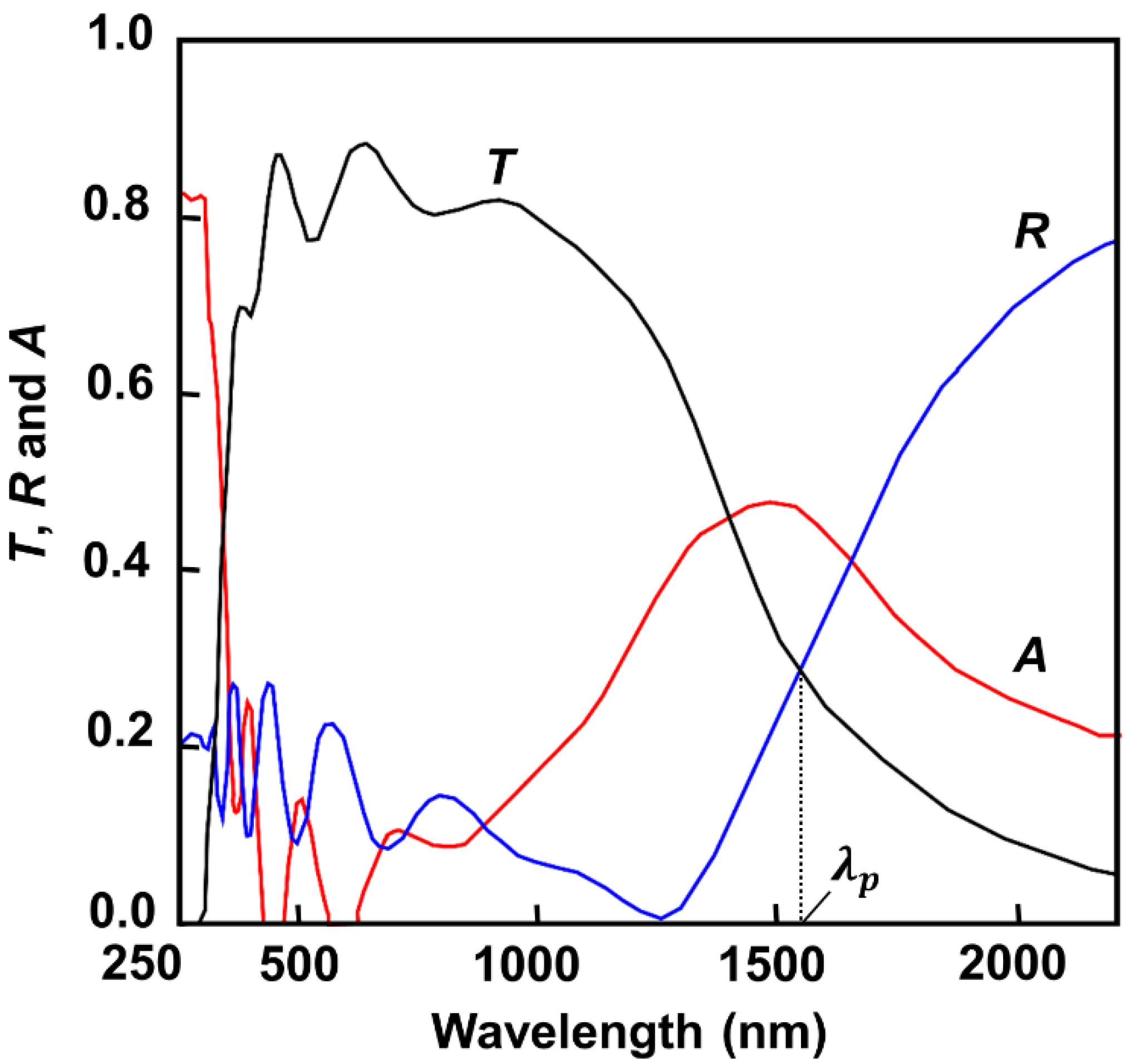
Regarding the electronic structure of the ITO, there is an indirect band gap with an edge 2.8 eV, which can shift to higher values around 3.4 eV as a result of the B–M mechanism [22,43]. Additionally, a weak absorption was observed for photons with energy h around 2.3 0.1 eV (500 nm) associated with an indirect bandgap in the ITO electronic band structure [44], which can cause a weak charge carriers generation in the ITO film in the light beam spot, for example with interesting applications briefly discussed in Section 3 in the LC engineering part. In addition, ITO exhibits another indirect band gap approximately around 1.9 eV (at 652 nm) formed by the oxygen deficiencies (acting as defects) known as orange emission [45]. The latter gives a strong emission, as a result a probe beam with such a wavelength is not able to induce the SPR effect. A typical absorption spectrum of the ITO thin film is shown in Figure 1.
2.2. Frequency-Dependent Conductivity of ITO Thin Film
Opto-electrical properties of ITO films can be investigated based on the classical Drude model. In ITO, the (valence) charge density almost exclusively (independent of charge mobility) determines the plasma frequency [46] (if the electron effective mass was kept constant [26]), which in turn, determines the reflectance edge. In the low charge density regime (i.e., m−3), the plasma frequency , at which the electrons undergo a resonance, is defined as [26,47]
where , , and are electron unit charge, electron effective mass, and the vacuum permittivity, respectively. In the high charge density regime where 1 (: is the plasma angular frequency) is fulfilled, the plasma frequency is modified as (: is the high frequency permittivity being 4 for ITO). For example, for ITO thin film, by a nonlinear change of the electron effective mass from 0.35 to 0.53 corresponding to the charge densities of 6.2 × 1019 cm−3, 1.4 × 1021 cm−3, respectively [48], the plasma frequency can be obtained equal to 375 THz, 1449 THz. In this case, the plasma (cut-off) wavelength , where the transmission equals the reflectance , can be obtained from [26],
where is the Plank constant, which gives 798 nm, 207.1 nm, correspondingly. Apparently, these values show the plasma frequency shift from near IR (for charge densities in the range of 1019 cm−3) to UV (for 1021 cm−3) range [49]. ITO is highly reflective at optical frequencies , whereas it is highly transparent at [50,51]. As a result, for exhibiting transparency in the visible range of the light, the charge density would be tuned carefully in order to lead to a plasma frequency in the near IR or IR regions. High free charge density in conventional metals, such as Cu or Ag (61022 cm−3–8 1022 cm−3), hampers electrical manipulation of their optical properties.
It can be concluded that ITO as a transparent electrode in NLC cells has unavoidably semiconducting behavior in the visible light beam, which allows diffusion and redistributions of the photogenerated-charge carriers along the ITO interface, which in turn, supports the SPR effect.
Conductivities of metal oxides such as tin oxide or indium–tin oxide (ITO) are frequency-dependent [52]. Generally speaking, there is a duality in the electro-optical behavior of the ITO thin film, as it acts metallic in the microwave band exhibiting high conductivity, while semiconducting in the visible spectrum exhibiting much lower conductivity.
When an ITO film is shone by a light beam with an angular frequency , the effective conductivity can be obtained from Drude model [50] as,
where is the angular frequency, is the electron relaxation/scattering time, which has an effective value about 3.310−15 s for ITO thin films [47], and () is the Drude DC conductivity. The effective conductivity is a complex quantity with real and imaginary parts, i.e., and , of:
From above the relations, it can be deduced that in the low-frequency limit (i.e., ), when the input beam is in the IR region, ITO shows the maximum conductivity as , where , (see in Figure 2). By increasing the frequency , the imaginary part of the effective conductivity, , grows beyond the real part, , as both quantities are kept lower than the DC conductivity, . For example, for a visible light beam with a wavelength of 500 nm, and the associated angular frequency 37681012 rad/s (counting for 12.43 rad), the real and imaginary parts of effective conductity read 6.4 and 8, which give the effective conductivity equal to 8.01. In the high-frequency regime (i.e., ), both terms go to zero but with a faster rate, as ITO acts as an insulator with almost zero conductivity when lit by a very-high-frequency light beam (seen in Figure 2).
2.3. ITO Conductivity in Very Low DC Operating Regime
If the electrostatic potential, , in the ITO thin film is much smaller than the Fermi energy , the ITO layer can be approximated as being in the equilibrium state. In general, the electrochemical potential in the Fermi level located in the conduction band, i.e., , can be approximated as [53], which implies that , where is the Fermi energy. For instance, the electrochemical potential is about 0.7 eV for an ITO thin film with a thickness of 200 nm grown on the glass [26]. Because of the B–M shift, at an equilibrium state, only the charge carriers above the Fermi level are free to move and contribute to the conductivity. Since ITO is a degenerate n-type semiconductor, the thermally available free charge density at equilibrium state () above the B–M barrier at temperature, , can be estimated as [54,55],
where is referred to as the effective density of states in the conduction band, the term (the product of Boltzmann constant and temperature ) is 25.7 meV at room temperature. Hence, for example, if 1026 m−3 and = 0.6 eV, then the maximum available (thermally excited) free charge density can be obtained as 1016 m−3. The DC electric field screening by this amount of mobile charge density is infinitesimal. The so-called Thomas–Fermi screening length, , can be obtained from [56],
where is the electron effective mass, is the plank constant divided by 2π. For the 1016 m−3, and is 147 μm, which shows the minor damping of the static electric field in the ITO thin film in the near equilibrium condition. If ITO acts metallic, then is of the order of several nm; In this condition, it would be expected that electric field is completely screened in the ITO film, which implies the suppression of the fringe electric field formation specified with tangent element to the interface. As a result, in the metallic operating regime of ITO, the SPR effect cannot occur.
In the non-equilibrium condition when , reads [57],
Due to the irregularity in the band structure of the ITO film, a minimum energy equal to is required in order to make ITO cut through its conduction band, giving rise to the free charge carriers, hence, behaving in a quasi-metallic manner. This amount of energy can be provided for example by an optical stimulus [41] or an electrostatic field.
In the low DC voltage operating regime when the ITO thin film is lit by a visible light beam, hence operating with low conductivity, hot photogenerated-charge carriers in the beam spot can be swept away by the DC electric field. This leaves behind regions with very low charge densities of opposite charge carriers (densities diminished due to recombination process with the residing ions) which locally induces semiconducting behavior in the ITO thin film in the beam spot. The self-action of the light beam in some applications will be discussed in the next section.
3. A Brief Review of the Self-Action of a Visible Light Beam in the NLC Cells Biased with a DC Electric Field
In the experimental investigations conducted on the NLC cells with initial planar alignment, it was verified that treating the LC cell surfaces with a non-photo-conducting polymer layer (such as LQ1800 polyimide) could weaken or disable (depending on the cell configuration and light beam incidence direction) the SPR effect in cells filled with pure E7 LC by means of decreasing the degree of the electric field modulation inside the LC film [58]. However, the use of an alkyne compound LC (such as BL001) caused effective director field realignments to take place due to a higher sensitivity of the director field realignment in the electric field. Hence, by suppressing charge carriers photogeneration inside the aligning layer and bulk LC, photo-induced charge carriers’ redistributions in the ITO layers were verified. The mechanism was highly sensitive to the applied optical wavelength [58].
In the NLC cells filled with E7 LC and equipped with an ITO thin film coated with polyvinyl alcohol (PVA)—a polymeric film exhibiting photoconductivity [59]—as a common anchoring agent in the LC cells, the DC voltage drop was verified on the double thin layers (i.e., polymer/LC and ITO/LC interfaces) when shone by a homogeneous laser beam profile in a planar cell [11]. It was attributed to the neutralization of the accumulated ions by the photo-induced charge carriers under the recombination process. Minority charge carries, i.e., holes, dominate in both the ITO and polymer layers, forming barriers at the interfaces. Therefore, the DC voltage locally drops (which can be understood from the physics of a plane capacitor resembling the LC cell). Biased low DC voltages ( V in test cells with thickness of 30 m) were completely screened at the LC film interfaces, while by increasing the voltage magnitude, the screening degree decreased reaching a constant value [11].
In sum, all evidences imply that ITO can contribute in the SPR effect independent of the LC mixture and the orientation layers due to the semiconducting operation mode in the visible light, which is correlated with its specific optical characteristics. Thanks to the SPR effect, stronger director field realignments and control can be achieved.
The impact of the SPR effect on the electro-optical behavior of the pure NLC cells is discussed further in the following sections.
3.1. The SPR Effect Manifested in the Formation of the Aberration Patterns
Aberrational patterns are specified with concentric ring structure in the far diffraction zone. They have asymmetric shapes [60] with a kink at the corner seen in symmetric LC cell designs subject to a DC electric field [4,5,61].
From the aberration pattern, information regarding director field reorientation [60,62,63] and the ratio of elastic constants [64] can be extracted. In the case of director field reorientation by the light electric field E, information regarding self-focusing or self-defocusing can be obtained from the investigation of the aberrational patterns [63]. If director field tends to take alignment along the light field E, refractive index change of the LC is positivecategorized as self-focusing. A negative change in refractive index can cause self-defocusing of the light beam attributed to an opposite trend of director field reorientation.
Aberrational patterns with specific orientational properties can form in pure NLC cells illuminated by a visible light beam due to the SPR effect [4,5,61]. The efficiency of the SPR effect depends on the light wavelength [4,61]. Studies on the asymmetry (the horizontal divergence) of the aberrational patterns and the number of rings in the far-field diffraction zone were conducted on transparent NLC cells equipped with ITO electrodes and biased with low DC voltage. They showed that with increasing the wavelength within a spectral range of 458–647 nm (corresponding to the photon energy range of 2.7–1.92 eV) the efficiency decreased to zero (the phenomenon was not seen at 647 nm). The orientational SPR effect became manifest in the aberrational patterns formation independent of the light beam polarization [4,5,61]. It was effectively exploited at very low optical power irradiation (few milliwatt (mW)) and low biased DC voltage (a few volts) in the visible range of the light beam [4,5,61] before smoothing of the director field reorientation happened (when the maximum possible realignment was achieved) [16].
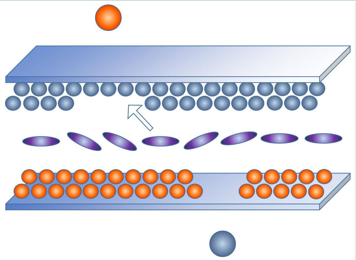
In Figure 3, in the electrode connected to the battery anode, the photogenerated-charge carriers (electron-hole pairs) can get spatially separated more effectively [4,5,61]. The fast photogenerated electrons participate in the photo-induced current density under the drift mechanism, whereas the slow photo-generated holes diffuse in the beam spot along the electrodes hence neutralizing the static negative charge ions residing in this region [13].
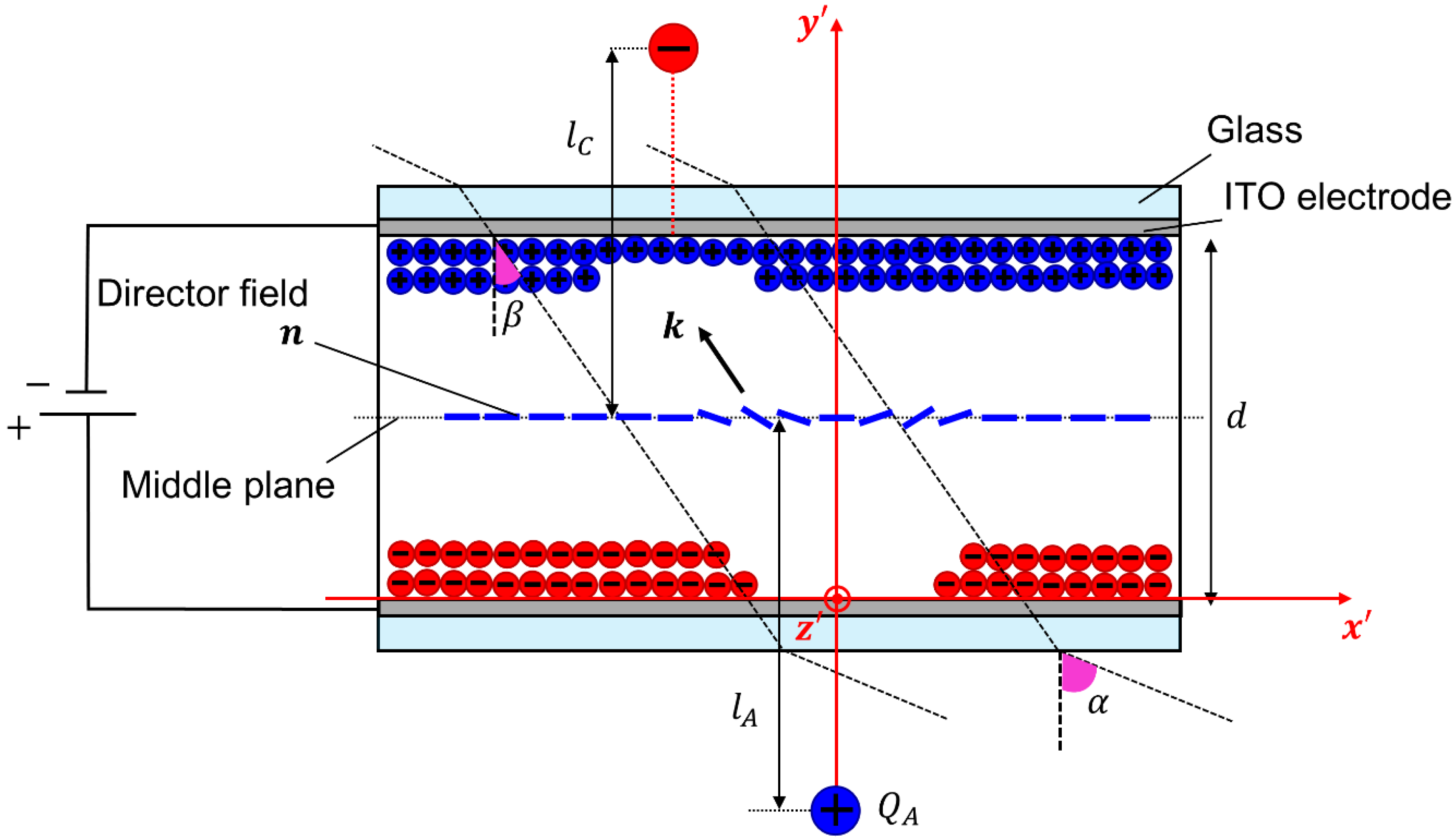
For simulating the electric field in the LC for a planar test cell made from ITO electrodes and filled in with pure NLC, the redistribution of the surface charges responsible for the screening of the electric field under the self-action of light were modeled by assumption of two point charges (with signs opposite to the screening charges at the corresponding surfaces), i.e., and , induced at the electrodes connected to the anode and cathode polarities of the battery, respectively, with opposite signs as the surface charges sit on corresponding surfaces [5] (see Figure 3). The photo-induced charges can be determined from measuring the photo-induced external current through the circuit [13]. The electric field has a fringe profile at the ITO surface characterizing the semiconducting nature of the ITO layer (associated with an electric potential gradient) under visible laser beam illumination [5].
In electric field modeling, the point charges and were adjusted out of the ITO planes at distances and ( along the beam propagation axis) relative to the cell midplane in order to give a suitable model of the fringe electric field profile in the LC cell [5]. By considering the Gaussian profile of the laser beam, these point charges located out the electrode surfaces can provide a good approximation of the real electric field profile induced by redistributed surface charge densities (with Gaussian profiles) at the beam spot [5]. Hence, the electric field inside the LC volume, for example, in the central plane located at , where is the cell thickness, can be obtained from [5],
where the unit vectors , , and are along the Cartesian coordinate axes , , and ; is the dielectric permittivity in the DC field; is the refraction angle at the LC boundary with the substrate, which can be approximated as ; is the incident angle of the light beam with respect to the axis; and is the LC effective extraordinary refractive index. In relation (10), the term gives the reduced electric field in the LC cell in the laser-off state when the electric field is screened by the surface charges by a factor [5].
3.2. Generation of Optical Vortices in the NLC Context Due to the SPR Effect
In the NLCs, umbilical defects (in short “umbilics”) [65,66] can act as a topological matter context for the generation of the optical vortices (OVs). In Laguerre–Gauss beams, OVs carry orbital angular momentum (OAM). They are characterized by phase singularity along their beam propagation axis [67]. OVs have found application in efficient optical tweezers to trap low- and high-index particles with low optical intensities [68,69], in high-resolution astronomical imaging [70], in optical coronagraph with 95% intensity contrast [71], and in classical [72] and quantum [73] optical communication systems.
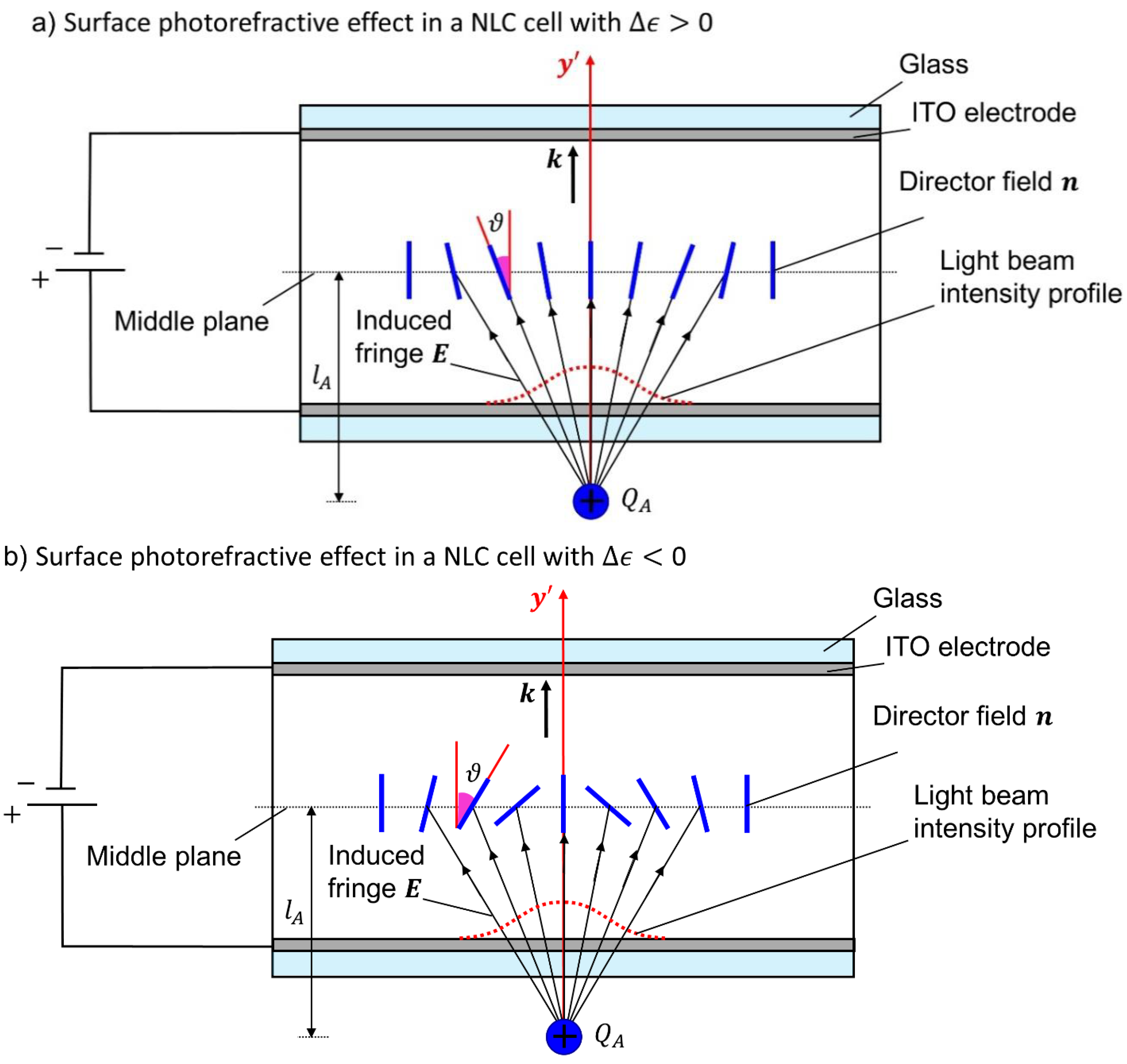
Electric field in the illuminated NLC cell by a light beam at normal incident to the surfaces can have a fringe profile in the planar configuration as a result of the SPR effect. The induced fringe electric field inside the LC volume is capable of realigning NLCs (with positive and negative dielectric anisotropies) from initial homeotropic alignment when shone by a low laser power (of a few mW) at a reduced threshold voltage [74,75,76,77], as schematically shown in Figure 4. Independent of the sign of the dielectric anisotropy, radial director field distributions in the transverse plane were seen as a result of director realignments from initial homeotropic alignment induced by the SPR effect [74,75,76,77]. This leads to the formation of optical vortices (OVs) [78,79,80] from an incident plane wave.
As discussed, according to the beam profile, the electric field screening can be removed under the self-action of a light beam. Since this mechanism is more effective at the anode electrode connected to the positive polarity of the DC voltage (verified from the elongation direction of the aberrational patterns [61]), the modeling of the induced electric field was roughly simplified here by assuming only one positive point charge located near the anode at a distances relative to the cell midplane. It represents the redistributed surface electric charges at the corresponding electrode [74,75,76]. The simplified model was able to describe the generation of OVs in the corresponding test cells well [74,75,76].
At the first attempts, OVs were generated with low efficiency (with a maximum value of about 30% for NLC with negative anisotropy) [74]. However, high conversion efficiency (of incident plane wave to the helical waves) of above 95% was theoretically predicted in NLC with negative dielectric anisotropy by defining small LC film thickness (about 25 μm) and low optical birefringence (about 0.1) where a high degree of director field realignment was attained [76]. The technique developed by Kravets and co-workers [77] based on the optimum application of the DC electric field in the common NLC cells leads to a low optical phase delay of π. Then, the OVs are generated with high efficiency (>90%) and purity, since the NLC template acts as a half-wave plate providing the maximum conversion efficiency [77].
According to the literature, the SPR effect was verified under the condition of “low electric field and low optical power” in all cases studied. It was found that the DC voltage drop is usually between 0.5 to 1 in the pure NLC [11], which means an addressed voltage 2 V can usually compensate the voltage drop and drive the LC realignment above the Fréedericksz threshold. On the other hand, the photo-induced electric field (originated from the photogenerated-charge carriers) in low optical powers would be above the Fréedericksz threshold field as being able to induces the director field reorientation.
3.3. SPR Effect-Assisted Formation of Umbilical Defects in an NLC Cell Made from a Photo-Responsive Substrate
The photorefractive effect [81] was verified in the ITO electrode due to the charge carriers’ accumulation at the boundary of the ITO with an insulator in the presence of a static electric field [82,83,84,85]. The induced charge redistribution, in addition to the modulation of the ITO refractive index and voltage drop, can also induce a secondary refractive index modulation in the LC film through the SPR effect in the low-power laser beam regime.
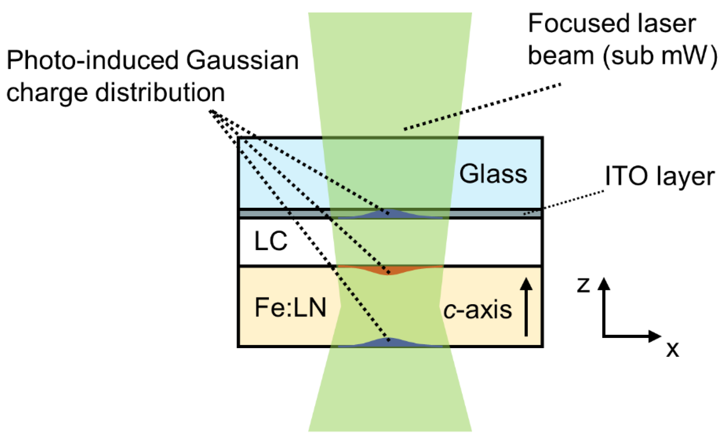
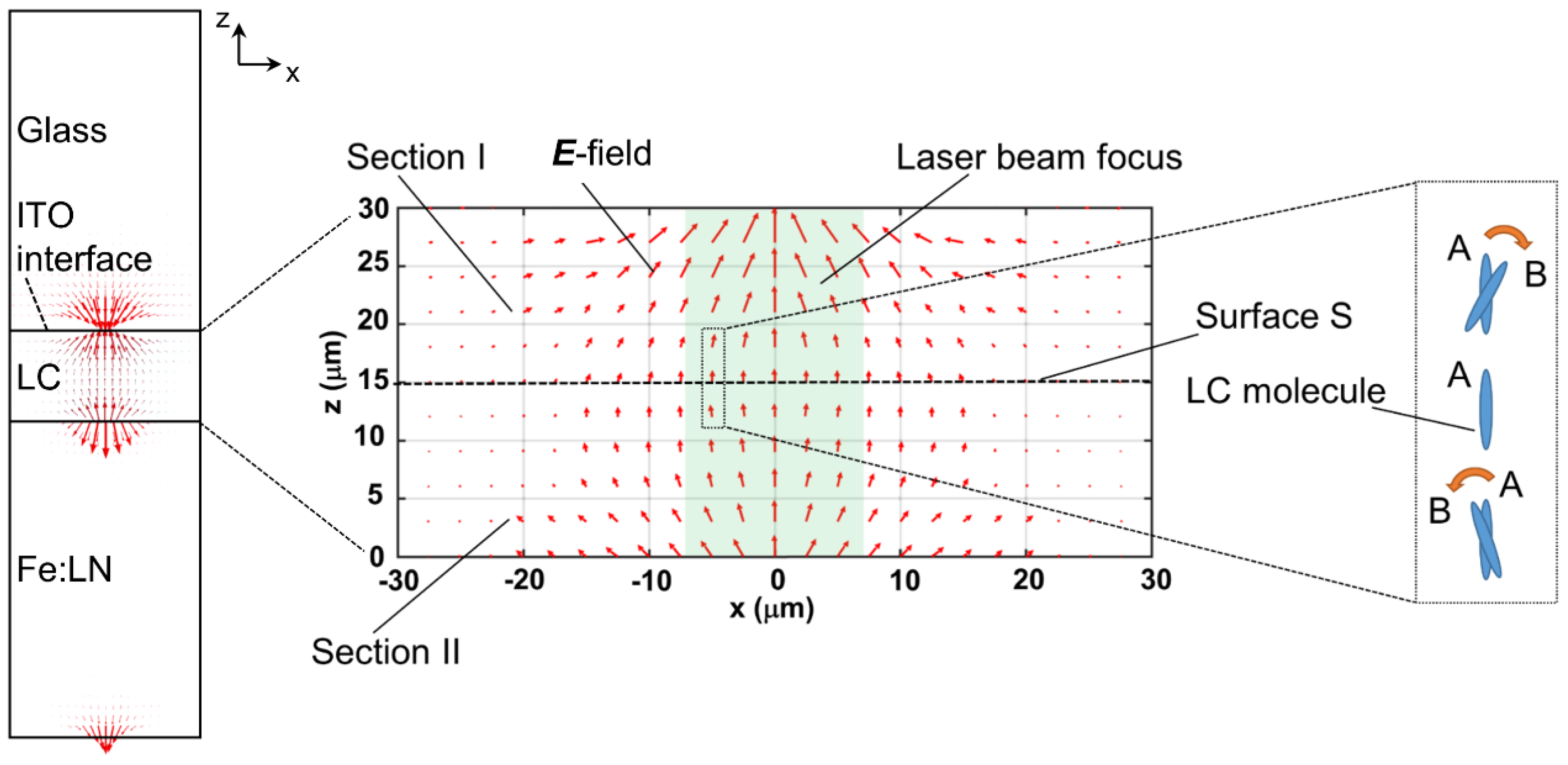
The SPR effect can generate and support umbilical defects (characterized as non-singular topological defects) in the NLC cells with photo-responsive substrate of a z-cut ferroelectric material, i.e., iron-doped lithium niobate (Fe:LiNbO3 or in short Fe: LN) covered with an ITO-equipped glass slab, as schematically shown in Figure 5. They act as context for the generation of OVs [19]. Here, photo-responsive substrate acts as a source of nonuniform photovoltaic electric field present in the LC film. In such test cells, the director field reorientation from an initial homeotropic alignment (provided by an anchoring agent) can take place under the action of an optically assisted fringe electric field distribution in the LC film (Figure 6) [19]. The fringe structure of the induced electric field is provided from both the photo-induced charge carriers’ accumulation at the surfaces of the ferroelectric slab, as well as in the ITO layer in the beam spot [19].
As seen, the fringe electric field stemming only from the photo-induced charge carriers’ distributions in the ferroelectric subtract is not capable of inducing the umbilical defects with spatial structure in the LC media as introduced by Rapini [66] in the cells without ITO equipment (the topological defects were formed only at the boundary surfaces of the LC layer) [17]. The umbilics are characterized by topological phase singularities extended along the test cell at the beam exposure center where the initial homeotropic alignment of the LC was kept fixed [19]. They can form when the electric field structure is effectively modified due to the induced fringe electric field distribution near to the LC border with the coated glass slab equipped with the ITO [19]. The radial realignment of the LC director field in the transverse plane comparable to an optical q-plate with radial geometry [86] can be supported in the whole LC volume [19].
4. Conclusions
The very common electrode in the LC cells, i.e., ITO, is well known for its refractive index modulation property. In the regimes of low addressed electrostatic potential and visible optical power, it can act quite semiconducting due to the charge carriers’ redistributions with a low density in the laser beam spot. As a result, the screening of the electric field on the LC film can be effectively removed by the action of the light beam when initially (at the laser off state) no realignment was observed even at voltages well above the threshold. This was attributed to the action of ions sitting at the border interfaces of the LC film while the B–M effect at the transparent electrode can be speculated as a cause.
The photorefractive effect in the ITO-equipped NLC cells was reported and utilized in the diffraction gratings in wave-mixing studies, the creation of hyperbolic umbilic caustics, and OVs through umbilical defect generation in NLC cells in optically assisted modified electric field profiles from initial uniform and fringe-shaped profiles, respectively.
A challenge was the understanding of the sources of the SPR effect in the NLC cells; it was found that the electron-hole-pair production and subsequent transport can happen in the ITO thin layer in addition to the orientant, where the residing charge carriers in the beam spot can be effectively neutralized due to the photo-induced low conductivity. In the semiconducting operating mode of the ITO layer, a fringe electric field with its tangent element to the LC confining surfaces (equipped with ITO) was induced which results in the LC director field realignment parallel to the cell surfaces (irrespective of the sign of the dielectric anisotropy), hence the SPR effect.
This review paper aimed to track some of the efforts that were made to realize and utilize the photorefractive effect in NLC cells in the static electric field, while emphasizing the key supporting role of the transparent electrode, i.e., ITO.
Funding
Funding by the German Research Society (DFG with project STA 425/44-1) is highly acknowledged.
Acknowledgments
The author is grateful to Ralf Stannarius for all his kind editions and challenging and fruitful discussions.
Conflicts of Interest
The author declares no conflict of interest. The funders had no role in the design of the study; in the collection, analyses, or interpretation of data; in the writing of the manuscript, or in the decision to publish the results.
References
- Ballman, A.A. Growth of Piezoelectric and Ferroelectric Materials by the CzochraIski Technique. J. Am. Ceram. Soc. 1965, 48, 112–113. [Google Scholar] [CrossRef]
- Nassau, K.; Levinstein, H.; LoIacono, G. Ferroelectric lithium niobate. 2. Preparation of single domain crystals. J. Phys. Chem. Solids 1966, 27, 989–996. [Google Scholar] [CrossRef]
- Yariv, A.; Yeh, P. Optical Waves in Crystals; Wiley: New York, NY, USA, 1984; Volume 5. [Google Scholar]
- Zolot’Ko, A.S.; Budagovsky, I.A.; Kitaeva, V.F.; Ochkin, V.N.; Shakun, A.V.; Smayev, M.P.; Barnik, M.I. Orientational Interaction of a Light Beam and NLCs Subjected to External DC Field. Mol. Cryst. Liq. Cryst. 2006, 454, 407–809. [Google Scholar] [CrossRef]
- Budagovsky, I.A.; Zolot’Ko, A.S.; Smayev, M.P.; Barnik, M.I. Self-action of a light beam in nematic liquid crystals in the presence of a DC electric field. J. Exp. Theor. Phys. 2010, 111, 135–145. [Google Scholar] [CrossRef]
- Rudenko, E.V.; Sukhov, A.V. Optically induced spatial charge separation in a nematic and the resultant orientational nonlinearity. JETP 1994, 105, 1621–1634. [Google Scholar]
- Rudenko, E.V.; Sukhov, A.V. Photoinduced electrical conductivity and photorefraction in a nematic liquid crystal. JETP Lett. 1994, 59, 142–146. [Google Scholar]
- Rudenko, E.V.; Sukhov, A.V. Photorefractive Effect in Nematic Liquid Crystals: Ion-Diffusion Approach. Mol. Cryst. Liq. Cryst. Sci. Technol. Sect. A. Mol. Cryst. Liq. Cryst. 1996, 282, 125–137. [Google Scholar] [CrossRef]
- Zhang, G.; Montemezzani, G.; Günter, P. Orientational photorefractive effect in nematic liquid crystal with externally applied fields. J. Appl. Phys. 2000, 88, 1709–1717. [Google Scholar] [CrossRef]
- Zhang, J.; Ostroverkhov, V.; Singer, K.D.; Reshetnyak, V.; Reznikov, Y. Electrically controlled surface diffraction gratings in nematic liquid crystals. Opt. Lett. 2000, 25, 414–416. [Google Scholar] [CrossRef]
- Pagliusi, P.; Cipparrone, G. Extremely sensitive light-induced reorientation in nondoped nematic liquid crystal cells due to photoelectric activation of the interface. J. Appl. Phys. 2003, 93, 9116–9122. [Google Scholar] [CrossRef]
- Khoo, I.; Chen, K.; Williams, Y. Orientational Photorefractive Effect in Undoped and CdSe Nanorods-Doped Nematic Liquid Crystal—Bulk and Interface Contributions. IEEE J. Sel. Top. Quantum Electron. 2006, 12, 443–450. [Google Scholar] [CrossRef]
- Budagovsky, I.A.; Zolot’Ko, A.S.; Lobanov, A.N.; Smayev, M.P.; Tskhovrebov, A.M.; Averyushkin, A.S.; Barnik, M.I. Study of the photocurrent in liquid crystal cells exhibiting the photorefractive effect. Bull. Lebedev Phys. Inst. 2010, 37, 49–55. [Google Scholar] [CrossRef]
- Habibpourmoghadam, A.; Wolfram, L.; Jahanbakhsh, F.; Mohr, B.; Reshetnyak, V.Y.; Lorenz, A. Tunable Diffraction Gratings in Copolymer Network Liquid Crystals Driven with Interdigitated Electrodes. ACS Appl. Electron. Mater. 2019, 1, 2574–2584. [Google Scholar] [CrossRef]
- Ouskova, E.; Reznikov, Y.; Shiyanovskii, S.; Su, L.; West, J.; Kuksenok, O.; Francescangeli, O.; Simoni, F. Photo-orientation of liquid crystals due to light-induced desorption and adsorption of dye molecules on an aligning surface. Phys. Rev. E 2001, 64, 051709. [Google Scholar] [CrossRef] [Green Version]
- Budagovsky, I.A.; Ochkin, V.N.; Smayev, M.P.; Zolot’Ko, A.S.; Bobrovsky, A.Y.; Boiko, N.I.; Lysachkov, A.I.; Shibaev, V.P.; Barnik, M.I. Interaction of light with a NLC–dendrimer system. Liq. Cryst. 2009, 36, 101–107. [Google Scholar] [CrossRef]
- Habibpourmoghadam, A.; Jiao, L.; Reshetnyak, V.; Evans, D.R.; Lorenz, A. Optical manipulation and defect creation in a liquid crystal on a photoresponsive surface. Phys. Rev. E 2017, 96, 022701. [Google Scholar] [CrossRef] [Green Version]
- Habibpourmoghadam, A.; Jiao, L.; Omairat, F.; Evans, D.R.; Lucchetti, L.; Reshetnyak, V.; Lorenz, A. Confined photovoltaic fields in a photo-responsive liquid crystal test cell. In Liquid Crystals XXI; International Society for Optics and Photonics: Bellingham, WA, USA, 2017; Volume 10361, p. 1036112. [Google Scholar]
- Habibpourmoghadam, A. Theoretical Prediction of Umbilics Creation in Nematic Liquid Crystals with Positive Dielectric Anisotropy. ACS Omega 2019, 4, 21459–21468. [Google Scholar] [CrossRef] [Green Version]
- Neaman, D.A. Semiconductor Physics and Devices; IRWIN: Chicago, IL, USA, 2003; Chapter 10; p. 457. [Google Scholar]
- Ray, S.; Banerjee, R.; Basu, N.; Batabyal, A.K.; Barua, A.K. Properties of tin doped indium oxide thin films prepared by magnetron sputtering. J. Appl. Phys. 1983, 54, 3497–3501. [Google Scholar] [CrossRef]
- Ohhata, Y.; Shinoki, F.; Yoshida, S. Optical properties of r.f. reactive sputtered tin-doped In2O3 films. Thin Solid Films 1979, 59, 255–261. [Google Scholar] [CrossRef]
- Burstein, E. Anomalous Optical Absorption Limit in InSb. Phys. Rev. 1954, 93, 632–633. [Google Scholar] [CrossRef]
- Her, S.-C.; Chang, C.-F. Fabrication and Characterization of Indium Tin Oxide Films. J. Appl. Biomater. Funct. Mater. 2017, 15, 170–175. [Google Scholar] [CrossRef] [PubMed]
- Mazur, M.; Kaczmarek, D.; Domaradzki, J.; Wojcieszak, D.; Song, S.; Placido, F. Influence of thickness on transparency and sheet resistance of ITO thin films. In Proceedings of the Eighth International Conference on Advanced Semiconductor Devices and Microsystems, Smolenice, Slovakia, 25–27 October 2010; pp. 65–68. [Google Scholar]
- Kim, H.; Gilmore, C.M.; PiquéA; Horwitz, J.; Mattoussi, H.; Murata, H.; Kafafi, Z.; Chrisey, D. Electrical, optical, and structural properties of indium–tin–oxide thin films for organic light-emitting devices. J. Appl. Phys. 1999, 86, 6451–6461. [Google Scholar] [CrossRef]
- Alam, M.; Cameron, D.C. Investigation of annealing effects on sol–gel deposited indium tin oxide thin films in different atmospheres. Thin Solid Films 2002, 420, 76–82. [Google Scholar] [CrossRef]
- Hosono, H.; Ueda, K. Transparent conductive oxides. In Springer Handbook of Electronic and Photonic Materials; Springer: Cham, Switzerland, 2017; p. 1. [Google Scholar]
- Farhan, M.S.; Zalnezhad, E.; Bushroa, A.; Sarhan, A.A.D. Electrical and optical properties of indium-tin oxide (ITO) films by ion-assisted deposition (IAD) at room temperature. Int. J. Precis. Eng. Manuf. 2013, 14, 1465–1469. [Google Scholar] [CrossRef]
- Shi, J.; Lau, S.P.; Sun, Z.; Shi, X.; Tay, B.K.; Tan, H. Structural and electrical properties of copper thin films prepared by filtered cathodic vacuum arc technique. Surf. Coat. Technol. 2001, 138, 250–255. [Google Scholar] [CrossRef]
- Edwards, P.P.; Porch, A.; Jones, M.O.; Morgan, D.V.; Perks, R.M. Basic materials physics of transparent conducting oxides. Dalton Trans. 2004, 19, 2995–3002. [Google Scholar] [CrossRef]
- Ioffe, A.F.; Regel, A.R. Non-crystalline, amorphous and liquid electronic semiconductors. Prog. Semicond. 1960, 4, 237–291. [Google Scholar]
- Heeger, A.J. The Critical Regime of the Metal-Insulator Transition in Conducting Polymers: Experimental Studies. Phys. Scr. 2002, 2002, 30. [Google Scholar] [CrossRef]
- Mott, N.F.; Davis, E.A. Electronic Processes in Non-Cyrstalline Materials; Oxford University Press: Oxford, UK, 2012. [Google Scholar]
- Kaushik, D.K.; Kumar, K.U.; Subrahmanyam, A. Metal-insulator transition in tin doped indium oxide (ITO) thin films: Quantum correction to the electrical conductivity. AIP Adv. 2017, 7, 15109. [Google Scholar] [CrossRef]
- Lin, J.-J.; Li, Z.-Q. Electronic conduction properties of indium tin oxide: Single-particle and many-body transport. J. Phys. Condens. Matter 2014, 26, 343201. [Google Scholar] [CrossRef] [Green Version]
- Moss, T.S. The Interpretation of the Properties of Indium Antimonide. Proc. Phys. Soc. Sect. B 1954, 67, 775–782. [Google Scholar] [CrossRef]
- Fan, J.C.C.; Goodenough, J.B. X-ray photoemission spectroscopy studies of Sn-doped indium-oxide films. J. Appl. Phys. 1977, 48, 3524–3531. [Google Scholar] [CrossRef]
- Hamberg, I.; Granqvist, C.G.; Berggren, K.F.; Sernelius, B.E.; Engström, L. Band-gap widening in heavily Sn-doped In2O3. Phys. Rev. B. 1984, 30, 3240. [Google Scholar] [CrossRef] [Green Version]
- Hamberg, I.; Granqvist, C.G. Evaporated Sn-doped In2O3 films: Basic optical properties and applications to energy-efficient windows. J. Appl. Phys. 1986, 60, R123–R160. [Google Scholar] [CrossRef]
- Guizzardi, M.; Bonfadini, S.; Moscardi, L.; Kriegel, I.; Scotognella, F.; Criante, L. Large scale indium tin oxide (ITO) one dimensional gratings for ultrafast signal modulation in the visible spectral region. Phys. Chem. Chem. Phys. 2020, 22, 6881–6887. [Google Scholar] [CrossRef] [Green Version]
- Klein, A.; Körber, C.; Wachau, A.; Säuberlich, F.; Gassenbauer, Y.; Harvey, S.P.; Proffit, D.E.; Mason, T.O. Transparent Conducting Oxides for Photovoltaics: Manipulation of Fermi Level, Work Function and Energy Band Alignment. Materials 2010, 3, 4892–4914. [Google Scholar] [CrossRef] [Green Version]
- El Hichou, A.; Kachouane, A.; Bubendorff, J.L.; Addou, M.; Ebothe, J.; Troyon, M.; Bougrine, A. Effect of substrate temperature on electrical, structural, optical and cathodoluminescent properties of In2O3-Sn thin films prepared by spray pyrolysis. Thin Solid Films 2004, 458, 263–268. [Google Scholar] [CrossRef]
- Matino, F.; Persano, L.; Arima, V.; Pisignano, D.; Blyth, R.I.R.; Cingolani, R.; Rinaldi, R. Electronic structure of indium-tin-oxide films fabricated by reactive electron-beam deposition. Phys. Rev. B 2005, 72, 085437. [Google Scholar] [CrossRef]
- Lee, M.-S.; Choi, W.C.; Kim, E.K.; Kim, C.K.; Min, S.-K. Characterization of the oxidized indium thin films with thermal oxidation. Thin Solid Films 1996, 279, 1–3. [Google Scholar] [CrossRef]
- Palik, E.D. Handbook of Optical Constants of Solids; Academic Press: Cambridge, MA, USA, 1998; Volume 3. [Google Scholar]
- Porch, A.; Morgan, D.V.; Perks, R.M.; Jones, M.O.; Edwards, P.P. Electromagnetic absorption in transparent conducting films. J. Appl. Phys. 2004, 95, 4734–4737. [Google Scholar] [CrossRef]
- Liu, X.; Park, J.; Kang, J.-H.; Yuan, H.; Cui, Y.; Hwang, H.Y.; Brongersma, M.L. Quantification and impact of nonparabolicity of the conduction band of indium tin oxide on its plasmonic properties. Appl. Phys. Lett. 2014, 105, 181117. [Google Scholar] [CrossRef]
- Lee, H.W.; Papadakis, G.; Burgos, S.P.; Chander, K.; Kriesch, A.; Pala, R.; Peschel, U.; Atwater, H.A. Nanoscale Conducting Oxide PlasMOStor. Nano Lett. 2014, 14, 6463–6468. [Google Scholar] [CrossRef] [PubMed] [Green Version]
- Chen, C.-W.; Lin, Y.-C.; Chang, C.-H.; Yu, P.-C.; Shieh, J.-M.; Pan, C.-L. Frequency-Dependent Complex Conductivities and Dielectric Responses of Indium Tin Oxide Thin Films from the Visible to the Far-Infrared. IEEE J. Quantum Electron. 2010, 46, 1746–1754. [Google Scholar] [CrossRef]
- Levy, D.; Castellón, E. Transparent Conductive Materials: Materials, Synthesis, Characterization, Applications; John Wiley & Sons: Hoboken, NJ, USA, 2018. [Google Scholar]
- Neelakanta, P.S. Handbook of Electromagnetic Materials: Monolithic and Composite Versions and Their Applications; CRC Press: Boca Raton, FL, USA, 1995. [Google Scholar]
- Bechstedt, F. Many-Body Approach to Electronic Excitations; Springer: Berlin, Germany, 2016. [Google Scholar]
- NASA. Solid State Technology Branch of Nasa Lewis Research Center Fourth Annual Digest; NASA Technical Memorandum V. 105752; Lewis Research Center: Oak Ridge, TN, USA, 1992. [Google Scholar]
- Panda, S. Microelectronics and Optoelectronics Technology. Laxmi Publications Pvt. Ltd: New Delhi, India, 2009. [Google Scholar]
- Hamaguchi, C. Basic Semiconductor Physics; Springer: Berlin, Germany, 2010; Volume 9, pp. 443–510. [Google Scholar]
- Brennan, K.F. The Physics of Semiconductors: With Applications to Optoelectronic Devices; Cambridge University Press: Cambridge, UK, 1999. [Google Scholar]
- Pagliusi, P.; Cipparrone, G. Surface-induced PR-like effect in pure liquid crystals. Appl. Phys. Lett. 2002, 80, 168–170. [Google Scholar] [CrossRef]
- Lafemina, J.P. Photoconduction in polyimide. Chem. Phys. Lett. 1989, 159, 307–309. [Google Scholar] [CrossRef]
- Zolot’ko, A.S.; Kitaeva, V.F.; Sobolev, N.N.; Sukhorukov, A.P. Self-focusing of laser radiation in the course of the Fréedericksz transition in the nematic phase of a liquid crystal. Zh. Eksp. Teor. Fiz. 1981, 81, 933–941. [Google Scholar]
- Budagovsky, I.A.; Ochkin, V.N.; Smayev, M.P.; Zolot’ko, A.S.; Barnik, M.I. Asymmetric aberrational patterns at light beam self-action in nematic liquid crystals. In ICONO 2007: Coherent and Nonlinear Optical Phenomena, Proceedings of the SPIE; International Society for Optics and Photonics: Bellingham, WA, USA, 2007; Volume 6729, p. 67293E. [Google Scholar]
- Zel’dovich, B.Y.; Tabiryan, N.V. Orientational optical nonlinearity of liquid crystals. Sov. Phys. Uspekhi 1985, 28, 1059. [Google Scholar] [CrossRef]
- Kitaeva, V.F.; Zolot’ko, A.S.; Barnik, M.I. Orientational optical nonlinearity of absorbing nematic liquid crystals. Mol. Mater. 2000, 12, 271–293. [Google Scholar]
- Zolot’ko, A.S.; Kitaeva, V.F.; Kroo, N.; Sobolev, N.N.; Sukhorukov, A.P.; Csillag, L. Nature of the aberration pattern formed as the result of self-focusing of a light beam caused by reorientation of the director in liquid crystals. Zh. Eksp. Teor. Fiz. 1982, 83, 1368–1375, [J. Exp. Theor. Phys (Sov. Phys. JETP), 83 (4), 786 (1982)]. [Google Scholar]
- Brasselet, E. Tunable Optical Vortex Arrays from a Single Nematic Topological Defect. Phys. Rev. Lett. 2012, 108, 087801. [Google Scholar] [CrossRef]
- Rapini, A. Umbilics: Static properties and shear-induced displacements. J. Phys. 1973, 34, 629–633. [Google Scholar] [CrossRef]
- Basistiy, I.V.; Soskin, M.S.; Vasnetsov, M.V. Optical wavefront dislocations and their properties. Opt. Commun. 1995, 119, 604–612. [Google Scholar] [CrossRef]
- Gahagan, K.T.; Swartzlander, J.G.A.; Jr., G.A.S. Optical vortex trapping of particles. Opt. Lett. 1996, 21, 827–829. [Google Scholar] [CrossRef] [PubMed]
- Gahagan, K.T.; Swartzlander, G.A. Simultaneous trapping of low-index and high-index microparticles observed with an optical-vortex trap. J. Opt. Soc. Am. B 1999, 16, 533–537. [Google Scholar] [CrossRef]
- Tamburini, F.; Anzolin, G.; Umbriaco, G.; Bianchini, A.; Barbieri, C. Overcoming the Rayleigh Criterion Limit with Optical Vortices. Phys. Rev. Lett. 2006, 97, 163903. [Google Scholar] [CrossRef] [Green Version]
- Lee, J.H.; Foo, G.; Johnson, E.G.; Swartzlander, G.A., Jr. Experimental Verification of an Optical Vortex Coronagraph. Phys. Rev. Lett. 2006, 97, 053901. [Google Scholar] [CrossRef]
- Gibson, G.; Courtial, J.; Padgett, M.; Vasnetsov, M.V.; Pas’Ko, V.; Barnett, S.M.; Franke-Arnold, S. Free-space information transfer using light beams carrying orbital angular momentum. Opt. Express 2004, 12, 5448–5456. [Google Scholar] [CrossRef] [Green Version]
- Mair, A.; Vaziri, A.; Weihs, G.; Zeilinger, A. Entanglement of the orbital angular momentum states of photons. Nature 2001, 412, 313–316. [Google Scholar] [CrossRef] [Green Version]
- Budagovsky, I.A.; Shvetsov, S.A.; Zolot’Ko, A.S. Optical vortex generation in homeotropic NLCs in the presence of DC electric field. Mol. Cryst. Liq. Cryst. 2016, 637, 47–52. [Google Scholar] [CrossRef]
- Budagovsky, I.A.; Zolot’Ko, A.S.; Smayev, M.P.; Shvetsov, S.A. Formation of the light beam with wavefront screw dislocation at the photorefractive effect in nematic liquid crystal. Bull. Lebedev Phys. Inst. 2015, 42, 319–322. [Google Scholar] [CrossRef]
- Budagovsky, I.A.; Zolot’Ko, A.S.; Shvetsov, S.A. On the formation of vortex light beams at the surface photorefractive effect in NLC. Bull. Lebedev Phys. Inst. 2016, 43, 340–344. [Google Scholar] [CrossRef]
- Kravets, N.; Podoliak, N.; Kaczmarek, M.; Brasselet, E. Self-induced liquid crystal q-plate by photoelectric interface activation. Appl. Phys. Lett. 2019, 114, 061101. [Google Scholar] [CrossRef] [Green Version]
- Curtis, J.E.; Grier, D.G. Structure of Optical Vortices. Phys. Rev. Lett. 2003, 90, 133901. [Google Scholar] [CrossRef] [PubMed] [Green Version]
- Maleev, I.D.; Swartzlander, J.G.A.; Jr., G.A.S. Composite optical vortices. J. Opt. Soc. Am. B 2003, 20, 1169–1176. [Google Scholar] [CrossRef]
- Yao, A.M.; Padgett, M. Orbital angular momentum: Origins, behavior and applications. Adv. Opt. Photon. 2011, 3, 161–204. [Google Scholar] [CrossRef] [Green Version]
- Zhang, Y.; Burzynski, R.; Ghosal, S.; Casstevens, M.K. PR polymers and composites. Adv. Mater. 1996, 8, 111–125. [Google Scholar] [CrossRef]
- Feigenbaum, E.; Diest, K.; Atwater, H.A. Unity-Order Index Change in Transparent Conducting Oxides at Visible Frequencies. Nano Lett. 2010, 10, 2111–2116. [Google Scholar] [CrossRef]
- Melikyan, A.; Lindenmann, N.; Walheim, S.; Leufke, P.M.; Ulrich, S.; Ye, J.; Vincze, P.; Hahn, H.; Schimmel, T.; Koos, C.; et al. Surface plasmon polariton absorption modulator. Opt. Express 2011, 19, 8855–8869. [Google Scholar] [CrossRef]
- Yi, F.; Shim, E.; Zhu, A.Y.; Zhu, H.; Reed, J.C.; Cubukcu, E. Voltage tuning of plasmonic absorbers by indium tin oxide. Appl. Phys. Lett. 2013, 102, 221102. [Google Scholar] [CrossRef] [Green Version]
- Sorger, V.J.; Lanzillotti-Kimura, N.D.; Ma, R.-M.; Zhang, X. Ultra-compact silicon nanophotonic modulator with broadband response. Nanophotonics 2012, 1, 17–22. [Google Scholar] [CrossRef] [Green Version]
- Marrucci, L. Generation of Helical Modes of Light by Spin-to-Orbital Angular Momentum Conversion in Inhomogeneous Liquid Crystals. Mol. Cryst. Liq. Cryst. 2008, 488, 148–162. [Google Scholar] [CrossRef]
Figure 1.
Graph of the particular indium-tin-oxide (ITO) transmission, reflectance , and absorption spectrum for a thin film with thickness of 300 nm shown in enhanced resolution [26]. The plasma (cut-off) wavelength is shown. [Adapted from (Kim, H., Gilmore, A.C., Pique, A., Horwitz, J.S., Mattoussi, H., Murata, H., ... & Chrisey, D.B. (1999). Journal of Applied Physics, 86(11), 6451–6461, (https://doi.org/10.1063/1.371708).), with the permission of AIP Publishing].

Figure 2.
Simulated ITO conductivity as a function of light beam wavelength ranging from the UV to near IR spectrum. For an ITO thin film deposited on glass, the DC conductivity was supposed .
Figure 2.
Simulated ITO conductivity as a function of light beam wavelength ranging from the UV to near IR spectrum. For an ITO thin film deposited on glass, the DC conductivity was supposed .

Figure 3.
Removal of the DC electric field-screening by the light beam in a nematic liquid crystal (NLC) cell filled with a nematic LC with positive dielectric anisotropy, , causing a hyperbolic umbilic caustic. The redistribution of surface electric charges at the semiconductor (ITO) electrodes was modeled by two point charges, and , adjusted at distances and relative to te cell middle plane, respectively. The director field deflection from initial planar alignment in the induced fringe electric field is shown in the cell middle plane. is the light beam wave vector. This figure was inspired from Figure 6 in Ref. [4] and Figure 3 in Ref. [5].

Figure 4.
Director field reorientation in NLCs from initial homeotropic alignment with (a) positive, (b) negative dielectric anisotropy, respectively, as a result of the SPR effect leading to formation of the optical vortices. The light beam is normally incident onto the anode electrode, and the beam profile is shown by a red dashed curve. This figure was inspired from Figure 1 in Ref. [61].

Figure 5.
Schematic of a hybridized LC test cell equipped with an ITO coated glass [19]. (Reproduced from Habibpourmoghadam, A. (2019). ACS omega, 4(25), 21459–21468, (https://pubs.acs.org/doi/10.1021/acsomega.9b03158), further permissions related to the material excerpted should be directed to the ACS).

Figure 6.
Electric field distribution in the hybridized LC test cell made from a ferroelectric substrate and an ITO coated cover slab. The fringe electric field distribution inside the LC film is capable to induce splay umbilical defects in the initial homeotropic configuration [19]. (Reproduced from Habibpourmoghadam, A. (2019). ACS omega, 4(25), 21459–21468, (https://pubs.acs.org/doi/10.1021/acsomega.9b03158), further permissions related to the material excerpted should be directed to the ACS).

© 2020 by the author. Licensee MDPI, Basel, Switzerland. This article is an open access article distributed under the terms and conditions of the Creative Commons Attribution (CC BY) license (http://creativecommons.org/licenses/by/4.0/).
Share and Cite
MDPI and ACS Style
Habibpourmoghadam, A. Photorefractive Effect in NLC Cells Caused by Anomalous Electrical Properties of ITO Electrodes. Crystals 2020, 10, 900. https://doi.org/10.3390/cryst10100900
AMA Style
Habibpourmoghadam A. Photorefractive Effect in NLC Cells Caused by Anomalous Electrical Properties of ITO Electrodes. Crystals. 2020; 10(10):900. https://doi.org/10.3390/cryst10100900
Chicago/Turabian StyleHabibpourmoghadam, Atefeh. 2020. "Photorefractive Effect in NLC Cells Caused by Anomalous Electrical Properties of ITO Electrodes" Crystals 10, no. 10: 900. https://doi.org/10.3390/cryst10100900
Note that from the first issue of 2016, this journal uses article numbers instead of page numbers. See further details here.