Article

A Surface Photovoltage Study of Surface Defects on Co-Doped TiO2 Thin Films Deposited by Spray Pyrolysis

1
Department of Physics, Masinde Muliro University of Science and Technology, P.O. Box 190, Kakamega 50100, Kenya
2
Department of Physics and Astronomy, Botswana International University of Science and Technology, Private Bag 16, Palapye, Botswana
3
Department of Physics, University of Nairobi, P.O. Box 30197, Nairobi 00100, Kenya
*
Author to whom correspondence should be addressed.
Coatings 2016, 6(3), 30; https://doi.org/10.3390/coatings6030030
Submission received: 20 May 2016 / Revised: 12 July 2016 / Accepted: 14 July 2016 / Published: 22 July 2016

Abstract

:
Surface photovoltage (SPV) spectroscopy is a powerful tool for studying electronic defects on semiconductor surfaces, at interfaces, and in bulk for a wide range of materials. Undoped and Cobalt-doped TiO2 (CTO) thin films were deposited on Crystalline Silicon (c-Si) and Flourine doped Tin oxide (SnO2:F) substrates by chemical spray pyrolysis at a substrate temperature of 400 °C. The concentration of the Co dopant in the films was determined by Rutherford backscattering spectrometry and ranged between 0 and 4.51 at %. The amplitude of the SPV signals increased proportionately with the amount of Co in the films, which was a result of the enhancement of the slow processes of charge separation and recombination. Photogenerated holes were trapped at the surface, slowing down the time response and relaxation of the samples. The surface states were effectively passivated by a thin In2S3 over-layer sprayed on top of the TiO2 and CTO films.

1. Introduction

Surface photovoltage (SPV) spectroscopy is a non-destructive and fast technique for investigating optoelectronic properties at surfaces, interfaces, and in bulk by monitoring the illumination-induced changes in the surface voltage [1]. It provides important information, such as surface band bending, surface and bulk carrier separation and recombination, surface state distribution, and defect states by studying the photo-induced carrier separation and transfer in semiconductor materials. SPV has been used to study nanocrystalline semiconductors for various applications, and has recently received renewed attention for the study of integrated devices and micro-heterogeneous systems [2,3,4].
Doping of metal oxides with transition metals has led to the investigation of new materials with ferromagnetic properties for application in Spintronics devices, photocatalytic applications, as well as for energy conversion and storage [5,6,7,8]. Co dopant is optically active, imparts magnetic properties to TiO2 suitable for Spintronics device application, and enhances photocatalytic activity through the introduction of additional electronic defects in its lattice [9,10,11,12]. A few Co atoms are sufficient to create specific defect structures that trap charge carriers and induce ferromagnetic properties in TiO2 [11]. The enhancement of photocatalytic activity of Co-doped TiO2 (CTO) is associated with the red shift of the band gap due to the sp-d exchange interaction between band electrons and localized d electrons of the Co2+ substituting for Ti4+ cations, which shifts the conduction band downwards and the valence band upwards [13,14]. The red shift has also been associated with an increase in the density of defects, resulting in the formation of impurity bands, which may spread and overlap with the conduction band [5].
Anatase TiO2 consists of interconnected TiO6 octahedron, each in contact with eight neighbors via four corners and four edges. Local distortion in the octahedron induces energy levels below the conduction band. Incorporation of Co—which has a larger ionic radius than Ti—introduces additional distortions, increasing the density of defects [15]. Co2+ dopant substitutes for Ti4+, creating additional oxygen vacancies, which leave behind a lone electron pair. The electron pair reduces two Ti4+ ions to Ti3+. The oxygen defects are formed on the surface and in the bulk on TiO2. The vacancies in the bulk are less stable and may migrate to the surface. The oxygen vacancies, which act as electron donors, can be associated with both deep and shallow defects. The enhanced paramagnetic properties in Co-doped TiO2 have been linked to increased density of oxygen vacancies [9,10,11,12,13,14,15]. Co2+ defects are also introduced in the mid-gap near the oxygen and Ti3+-related trap states. Trap-to-trap transition of electrons can take place from a defect to a Co2+ state, from where they relax to ground state [10].
The electronic, structural, and electrical properties of thin films depend on the deposition methods. CTO films and nanostructures have been deposited by sol–gel [9,10], ball milling [14], spray pyrolysis [16,17], solvo-thermal [15], pulsed laser deposition [18,19], molecular beam epitaxy [20], reactive co-sputtering [21], and atomic layer deposition [22]. Chemical spray pyrolysis has the advantage that it is vacuum-free, allows for a wide variety of precursor choices and deposition parameters, and different precursor solutions can be mixed in different proportions before deposition to effectively dope the samples.
In this work, CTO thin films were prepared by spray pyrolysis from precursors with different compositions of Ti and Co salts. The composition was analyzed by Rutherford backscattering spectrometry (RBS), while optoelectronic properties were investigated using UV-Vis and SPV techniques. SPV is a photoelectric method that is very sensitive to changes in electronic states participating in charge separation, independent of whether it is at the surface, interface, or in the bulk [23].

2. Materials and Methods

To prepare the precursor solutions, 19.2 mL of Titanium isopropoxide (TTIP) was mixed with 28.8 mL of 2,4-Pentanedione solution. Absolute ethanol solvent was added and stirred to make 480 mL of solution. This was called solution A. Solution B was prepared by dissolving 43.2 mg of anhydrous CoCl2 in 50 mL of acetonitrile and stirring for 3 hrs. Different volumes of solution B were added to solution A in volumetric percentages varying from 0% to 50%. TiO2 films were obtained from solution A and Co-doped TiO2 (CTO) thin films from the mixture of solutions A and B by spraying for 5 min at a substrate temperature of 400 °C. RBS experiments were performed using a 2.0 MeV He+ ion beam at zero incidence and exit angle of 12°. The backscattered ions were detected at a scattering angle of 168°. The charge was 5 coulombs with measurement time of about 12 min. The optoelectronic defects were investigated by modulated surface photovoltage in the fixed parallel capacitor configuration [24,25], with the incident light modulated at 8 Hz. The SPV signals were detected using a high impedance buffer and a lock-in amplifier.

3. Results

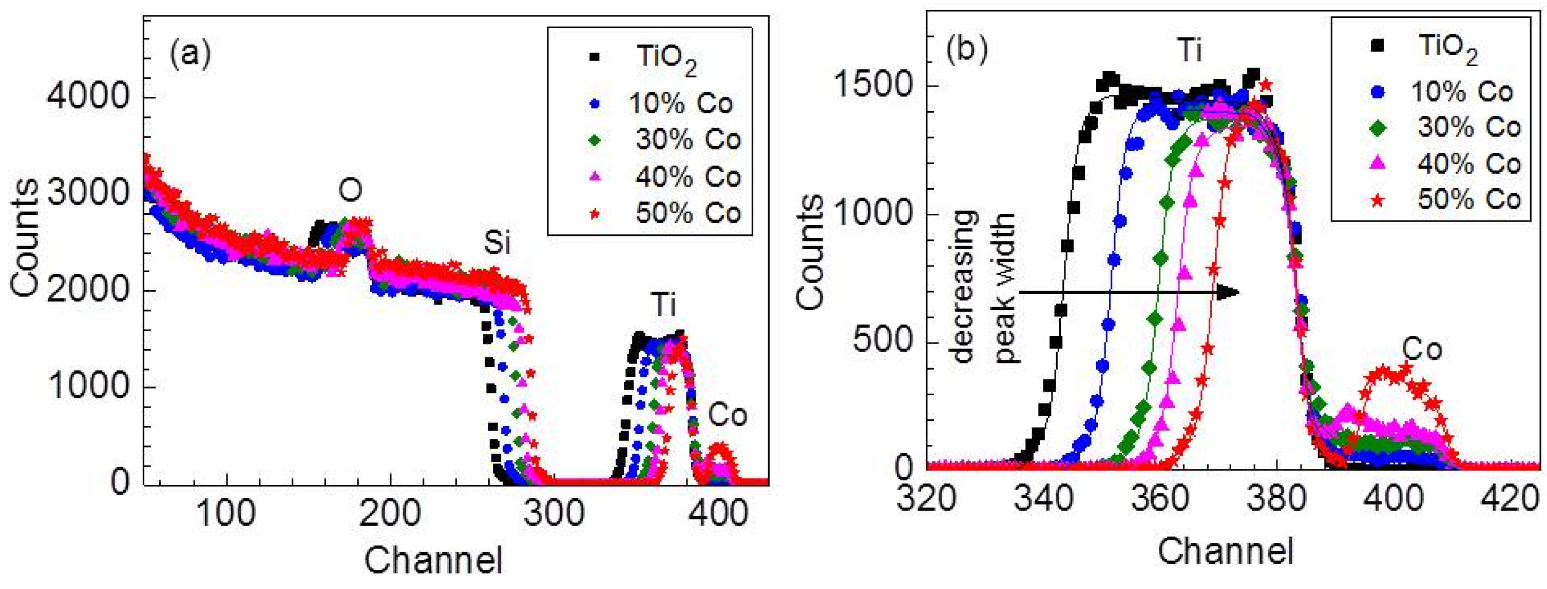
3.1. Compositional Analysis

Figure 1a shows the RBS spectra for the TiO2 and CTO thin films deposited on Crystalline Silicon (c-Si) substrates. The RBS signals from Co, Ti, Si substrate, and O were identified as indicated in the figure. The channel position of these signals depends on the atomic number of the elements detected. The heavier elements appear at higher channel numbers, corresponding to higher energy of the backscattered He+ ions after collision with the nucleus of that specific atom. The height/yield of the RBS signal is proportional to the amount of material present in the sample, and it depends on the scattering cross-section of the detected element. The width of the peak is proportional to the thickness of the probed sample and depends on the energy loss per unit depth of the detected element [26].
A decrease in the width of the RBS signals from Ti and Co and a shift of the signal from the surface of the c-Si substrate to higher channels was observed with an increase in the amount of CoCl2 in the precursor solution. A decrease in the width of the RBS signal is concomitant with a decrease in the film thickness. The height of the Co signal increased as a function of increasing amount of solution B in the precursor, which confirms the increase in the amount of Co in the CTO film. Figure 1b shows the Ti and Co signals from the RBS spectra fitted using Spewa software (Version 1.0, Institute of solid state Physics, Jena, Germany) based on the Nuno’s Data Furnace (NDF) code [27].
The thicknesses and atomic concentrations of the TiO2 and CTO thin films were extracted from fitting the spectra and from the integrals of the Ti and Co signals. The thickness for undoped TiO2 was 175 nm, and for the CTO films it ranged between 175 nm for 5 vol % and 60 nm for 50 vol % of CoCl2 in the precursor solution, as given in Table 1. The film deposition rate was dependent on the composition of the precursor solution, and decreased with an increase in the amount of CoCl2 in the solution. The Co atomic concentrations in the thin films obtained from fitting the RBS spectra as shown in Figure 1b amounted to between 0.43 at % and 4.51 at % for CTO films deposited from solutions containing 5 vol % and 50 vol % of CoCl3, respectively, as presented in Table 1.

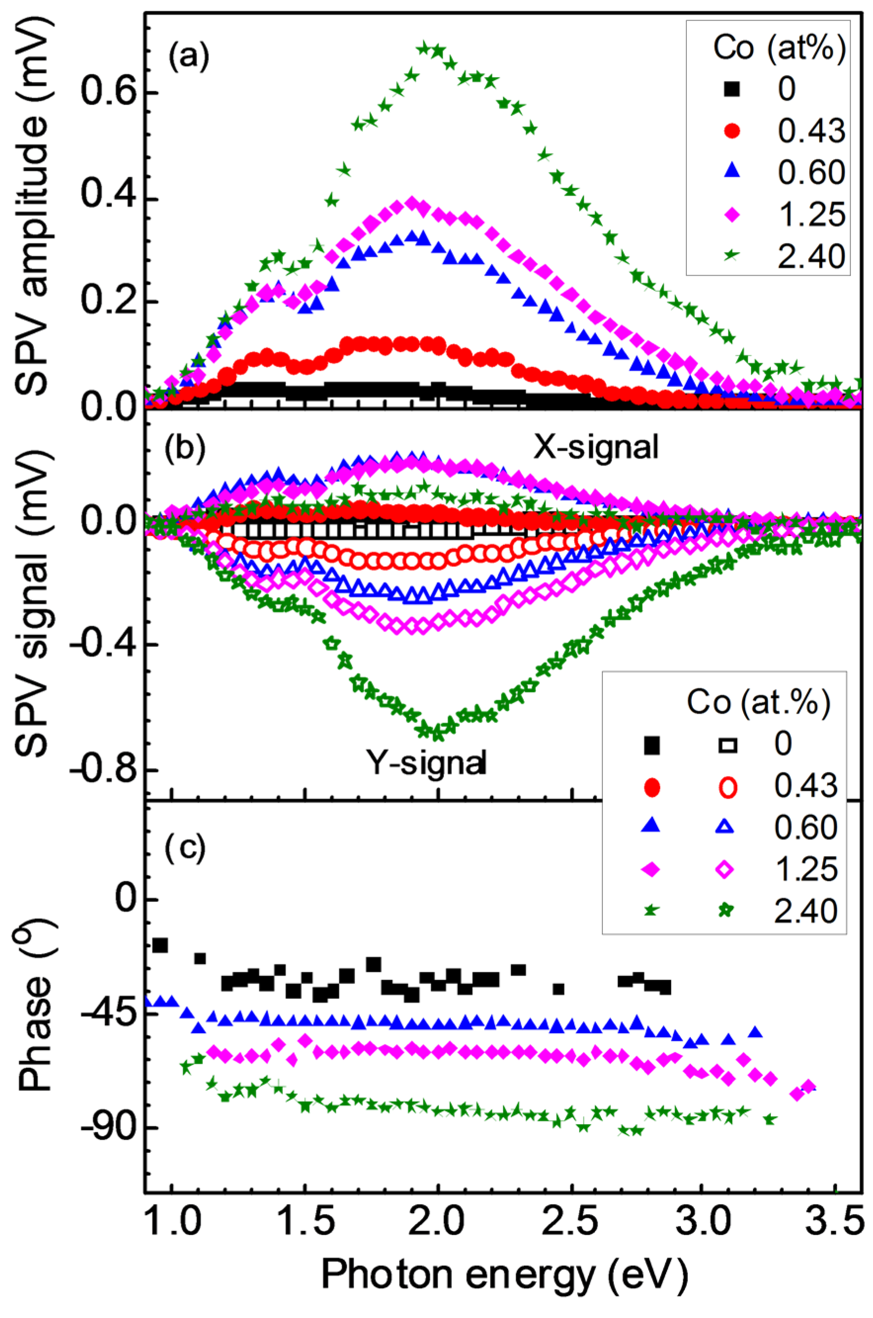
3.2. Modulated Charge Separation

The electronic defects in TiO2 and CTO thin films deposited on SnO2:F substrates were investigated by studying photogenerated charge separation under chopped light. In modulated SPV experiments, four signals are normally recorded using a lock-in amplifier. The in-phase (X-signal) and the phase shifted by 90° (Y-signal) with respect to the reference modulated signal gives information about the direction of separation of the photogenerated charge carriers and the time response of the sample to the modulation of the incident light. The spectral dependent SPV amplitude is the square root of the sum of the squares of the X and Y signals, while the phase angle is the inverse tangent of the ratio between the Y and X signals [27,28].
Figure 2a shows SPV amplitudes for the TiO2 and CTO thin films doped with 0.43, 0.60, 1.25, and 2.40 at % of Co. The onset energy of the signal was 0.96 eV for all samples (which is very low), compared to the absorption edge of TiO2 which has a band gap of 3.2 eV. The onset energy of the SPV signal is characteristic of the mobility edge and is expected to be close to the band gap energy for an ideal semiconductor. The SPV signal was therefore dominated by charge separation below the TiO2 band gap, which indicates the possibility of there being a high density of sub-band gap defect states.
The amplitude signal shows two peaks centered at 1.4 and 1.9 eV. Such peaks cannot be related to absorption peaks or peaks observed in spectroscopy, because the generation of an SPV signal could be a net result of several charge separation and recombination processes [28]. The two peaks therefore relate to energetic sub-band gap defects participating in charge separation and relaxation processes. The magnitude of the SPV amplitude at 1.9 eV increased from 0.036 mV for undoped TiO2 to 0.13, 0.32, 0.40, and 0.70 mV for dopant concentrations of 0.43, 0.60, 1.25, and 2.40 at %, respectively, while the film thickness decreased. The SPV amplitude is proportional to the number of photogenerated charge carriers separated in space, and the perpendicular distance between them. The magnitude of the SPV signal was not proportional to the film thickness, so it follows that the increase in the SPV amplitude was not due to an increase in the charge separation distance, but probably due to an increase in the density of the photogenerated charge carriers.
If the charge separation is caused by only one mechanism and the relaxation is due to recombination, the X and Y signals will have opposite signs [24,25,28], as shown in Figure 2b. The X-signal is positive, while the Y-signal is negative, indicating preferential separation of photogenerated electrons towards the substrate and holes towards the top surface. The X signal increased from 0.03 mV to 0.20 mV when the Co concentration in the film was increased from zero to 1.50 at %, but then dropped to 0.10 mV for higher Co amounts. There was no direct relationship between the Co concentration and magnitude of the X signal.
The absolute magnitude of the Y signal increased from 0.01 mV for undoped TiO2 to 0.11, 0.23, 0.32, and 0.67 mV when the amount of Co was increased to 0.6, 1.25, 1.50, and 2.4 at %, as shown in Figure 2b. This shows a direct correlation between the magnitude of the Y signal and the Co concentration in the CTO films. It can be concluded that the systematic increase in the SPV amplitude observed in Figure 2a with the increase in Co was mainly due to the concomitant increase in the Y signal. The Y-signal characterizes the phase shift between the SPV signal and the chopped light, and it corresponds to the slow increase or decrease of the SPV signal in relation to the half period of modulation [28]. The increase in the Y signal implies that the charge separation and/or relaxation were much slower than the modulation period of the chopped light. It follows that an increase in the Co dopant in the films slows down the charge separation and recombination processes.
Incorporation of Co ions introduces distortions in the octahedron of the TiO2 structure due to the difference in the ionic radii of Ti (0.605 Å) and Co (0.745 Å), enhancing the density of defect states and the concentration of the photogenerated charge carriers in the different trap levels [15]. Photoluminescence studies have shown that Co doping of TiO2 increases the lifetime of photogenerated carriers by introducing mid-band gap trap states associated with d states of cobalt, where an increase in the relaxation time of conduction electrons is observed before it undergoes recombination [10]. This explains the increase in the Y-signal with increasing Co dopant discussed above.
The phase angle of the SPV signal gives information about the direction of charge separation and the time response of the sample in relation to the period of modulation. For example, a positive X signal and a phase angle between 0° and −90° implies a single charge separation process with photogenerated electrons separated preferentially towards the internal interface [29]. In Figure 2c, the phase angle was observed to shift from −30° for undoped TiO2 to −48°, −60°, and −80°, with an increase in Co concentration to 0.6 at %, 1.25 at %, and 2.40 at %, respectively. A shift of the phase angle towards −90° means that the charge separation and/or relaxation processes became slower with increasing Co concentration [29,30,31,32].
The phase angle was independent of the photon energy, and so it can be concluded that in all samples, there was only one transport mechanism involved with charge separation and recombination processes within this spectral range. The shift in the phase angle corresponds to the increase in the Y-signal to more negative values, as discussed above (Figure 2b). The response times of the CTO samples to modulated light were increased by Co-doping. This could be due to enhanced trapping of the photogenerated holes in surface defect states.
Figure 3 shows the SPV signals of the bare In2S3 and CTO/In2S3 multilayer as a function of the Co concentration in the thin films. The onset of the SPV signal was 2.0 eV for bare In2S3 and 1.92 eV for TiO2/In2S3 and all CTO/In2S3 samples, independent of the Co concentration. The optical band gap of Ion Layer Gas Reaction deposited In2S3 thin films similar to those prepared in this work has been reported to be 2.0 eV [23]. The formation of SPV signal below the In2S3 band gap was therefore due to charge separation involving tail states below the In2S3 band gap and probably due to defect states at the CTO/In2S3 interface. The magnitude of the SPV amplitude (Figure 3a) of the TiO2/In2S3 was almost twice that of the CTO/In2S3 films. The SPV amplitude below 2.3 eV is higher for the TiO2/In2S3 and CTO/In2S3 multilayer’s compared to that of the bare In2S3 films, while there was barely any signal below 1.7 eV for all samples. There was dependence of the SPV signal on the Co dopant concentration. Compared to the SPV signals from the bare TiO2 and CTO films in Figure 2, we can conclude that the shallow defects centered at 1.4 eV were effectively passivated by the In2S3 over-layer.
The X signal was positive and the Y signal negative, which confirmed that the photogenerated electrons were preferentially separated toward the substrate and holes towards the surface. The phase angle for In2S3 was −47°, but shifted to about −60° for all the CTO/In2S3 samples (Figure 3b). This means that charge separation and recombination processes were slower for CTO/In2S3 samples compared to bare In2S3 films. The interface states at CTO/In2S3 heterojunctions played a role in the generation of the SPV signal in these samples by slowing down the processes.

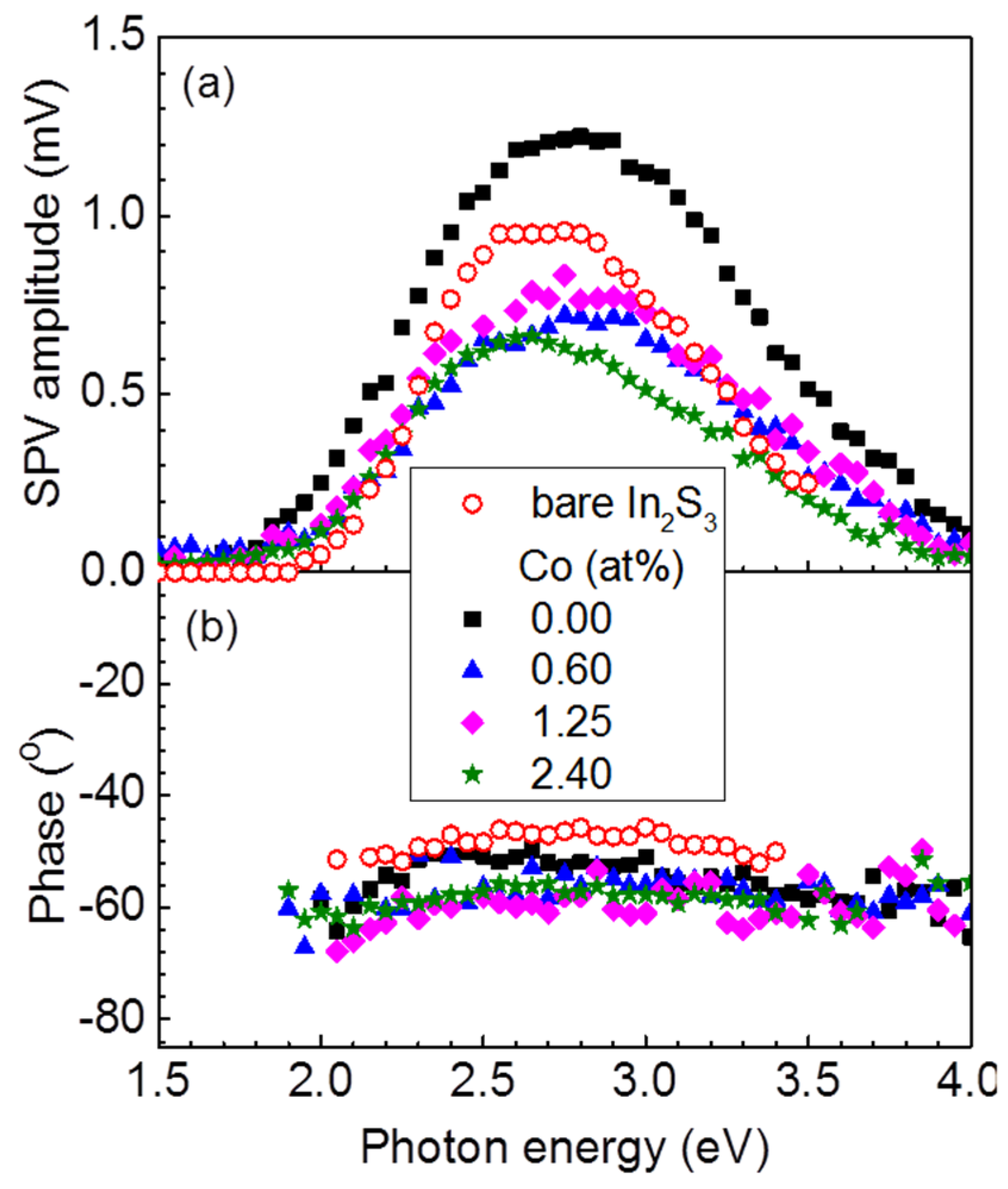
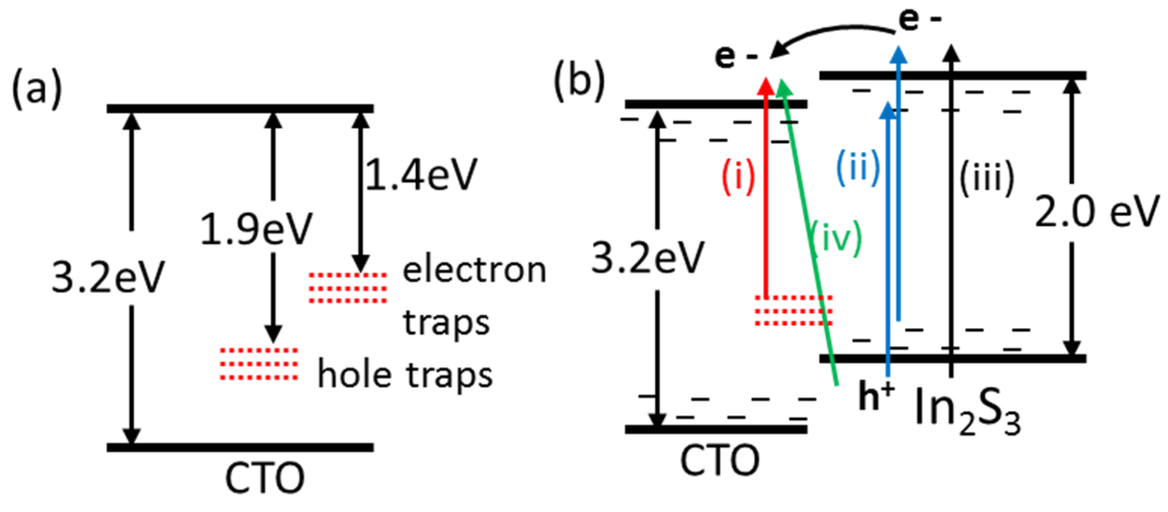
3.3. Band Gap Diagram for CTO/In2S3 Double Layer

Charge separation across the CTO/In2S3 interface can be understood using the band diagram given in Figure 4. The band gap of TiO2 was taken as 3.2 eV and that of In2S3 as 2.0 eV. Figure 4a indicates the presence of energetic surface defects centered at 1.9 and 1.4 eV below the conduction band, as deduced from Figure 2a. When the sample is illuminated, photon energies in this range are absorbed and the electrons trapped in this energetic defect state get excited into the conduction band, resulting in the SPV signal peaking at 1.4 and 1.9 eV. Photogenerated electrons excited into the conduction band are drawn into the bulk and holes towards the surface by the electric field created by the charge separation. The holes can be trapped at the surface states, resulting in delayed recombination. This is detected as an increase in the SPV Y-signal or an increase in the relaxation time of the conduction electrons in Photoluminescence measurements [6]. Increasing the Co dopant concentration enhanced the density of the surface states, where a larger number of holes got trapped, resulting in the higher amplitude of the Y-signal with increasing dopant amount, as observed in Figure 2b.
Introduction of Co2+ ions into a TiO2 lattice is known to induce structural distortion and hence an increase of defect states. Because Co2+ is incorporated with a charge of +2, oxygen vacancies are created to fulfill the charge neutrality condition [5]. Surface trap states have been attributed to the Ti3+ trap states and oxygen vacancies. Photoluminescence experiments have shown radiative recombination of trapped electrons at 0.7–1.6 eV below the conduction band edge of TiO2, which are associated with uncoordinated Ti3+ defects. Distribution of hole traps energetically positioned at 2.5–1.8 eV below the band gap are associated with hole traps due to oxygen vacancies [33,34,35]. Oxygen vacancies can form both shallow donor states as well as relatively deep trap levels located on the surface of TiO2. The defect states observed at 1.4 eV can be assigned to acceptor-like electron traps resulting from the Ti3+ defects, while the donor-like states localized at 1.9 eV below the conduction band can be associated with oxygen vacancies. With Co doping, the new oxygen vacancies create lone pair electrons in the vicinity of Ti4+ and reduce it to Ti3+, increasing the density of both oxygen vacancy and Ti3+ defect states [33].
By covering the TiO2 and CTO films with a thin In2S3 over-layer, the electronic defects on the surfaces were passivated and the SPV signals below the band gap disappeared. The SPV signal observed below the In2S3 band gap in Figure 3 was due to interface states existing at the CTO/In2S3 heterojunctions, which were not fully passivated. Some deep trap states remained at the interface and contributed to charge separation. As shown in Figure 4b, the SPV signal measured from the CTO/In2S3 double layer was due to several charge separation processes—namely, (i) photon absorption and excitation of electrons from the CTO/In2S3 interface states into the CTO conduction band; (ii) charge separation involving In2S3 tail states; (iii) band-to-band absorption in In2S3; and (iv) excitation from In2S3 valence band into CTO conduction band. It is also possible to have electrons excited from the defects states below the In2S3 band gap to states below TiO2 band gap. The SPV measurement does not distinguish between the different processes because it only captures the net charge separation mechanisms.
It can be concluded that the enhancement of the photocatalytic activity of CTO films and nanostructures observed in visible light is mainly due to an increase in the surface defects that are involved in charge separation. Substitution of Ti4+ by Co2+ causes distortions in the lattice structure and the creation of additional oxygen vacancies, which increases the density of the deep and shallow defect states in CTO films [15]. Co doping does not introduce new electronic defects, but increases the density and distribution of the already existing Ti3+ and oxygen vacancy defects. This behavior has led to an increase in the possible applications of TiO2 doped with transition metals in optoelectronics, especially under visible light.

4. Conclusions

Increasing the amount of Co dopant in the TiO2 thin film resulted in a decrease in the deposition rates. The optoelectronic properties of the CTO films showed dependence on the concentration of the Co dopant. The increase in the amplitude of the SPV signal was due to enhanced charge trapping by the surface defect states created by the substitution of Ti4+ by Co2+ in the TiO2 lattice. The formation of the SPV signal in the CTO/In2S3 double layer resulted mainly from charge separation in the In2S3 due to photon absorption and the excitation of electrons from the valence band into the conduction band of the In2S3 over-layer. The SPV onset energy of the CTO/In2S3 layers (1.92eV) was close to but slightly lower than the band gap of In2S3 (2.0 eV), and this can be due to the excitation of electrons from tail states below the band gap of In2S3. The holes can be trapped at the surface states, resulting in delayed recombination. This is detected as an increase in the SPV Y-signal or an increase in the relaxation time of the conduction electrons in PL measurements. This explains the enhanced photocatalytic activity in CTO films and nanostructures compared to undoped TiO2 reported in literature.

Acknowledgments

Authors appreciate the financial support from Deutscher Akademischer Austausch Dienst (DAAD), Christian.-Herbert. Fischer for laboratory space during sample preparation, technical support by Barth and constructive discussions with Elke. Wendler.

Author Contributions

Henry Wafula and Albert Juma conceived, designed, performed the experiments and wrote the paper; Robinson Musembi, Thomas Sakwa and Justus Simiyu analyzed the data.

Conflicts of Interest

The authors declare no conflict of interest. The sponsors had no role in the design of the study; in the collection, analysis, or interpretation of data; in the writing of the manuscript, and in the decision to publish the results.

References

  1. Kronik, L.; Shapira, Y. Surface photovoltage phenomena: Theory, experiments and applications. Surf. Sci. Rep. 1999, 37, 1–206. [Google Scholar] [CrossRef]
  2. Liqianga, J.; Xiaojun, S.; Jing, S.; Weimin, C.; Zili, X.; Yaoguo, D.; Honggang, F. Review of surface photovoltage spectra of nanosized semiconductor and its applications in heterogeneous photocatalysis. Sol. Energy Mater. Sol. Cells 2003, 79, 133–151. [Google Scholar] [CrossRef]
  3. Zhao, J.; Osterloh, F. Photochemical charge separation in nanocrystal Photocatalyst films: Insights from surface photovoltage spectroscopy. J. Phys. Chem. Lett. 2014, 5, 782–786. [Google Scholar] [CrossRef] [PubMed]
  4. Rotschild, A.; Levakov, A.; Shapira, Y.; Ashkenasy, N.; Komem, Y. Surface photovoltage spectroscopy study of reduced and oxidized nanocrystalline TiO2 films. Surf. Sci. 2003, 532–535, 456–460. [Google Scholar] [CrossRef]
  5. Ali, B.; Shah, L.; Ni, C.; Xiao, J.; Shah, S. Interplay of dopant, defects and electronic structure in driving ferromagnetism in Co-doped oxides: TiO2, CeO2 and ZnO. J. Phys. Condens. Mater. 2009, 21, 456005. [Google Scholar] [CrossRef] [PubMed]
  6. Tatlıdil, I.; Bacaksız, E.; Kurtulus, C.; Buruk, C.; Breen, C.; Sokmen, M. A short literature survey on iron and cobalt ion doped TiO2 thin films and photocatalytic activity of these films against fungi. J. Alloys Compds. 2012, 517, 80–86. [Google Scholar] [CrossRef]
  7. Mital, G.; Manoj, T. A review of TiO2 nanoparticles. Chin. Sci. Bull. 2011, 56, 1639–1657. [Google Scholar]
  8. García-Mota, M.; Vojvodic, A.; Abild-Pedersen, F.; Nørskov, J. Electronic origin of the surface reactivity of transition-metal-doped TiO2 (110). J. Phys. Chem. 2013, 117, 460–465. [Google Scholar] [CrossRef]
  9. Barakat, M.; Hayes, G.; Shah, S. Effect of cobalt doping on the phase transformation of TiO2 nanoparticles. J. Nanosci. Nanotechnol. 2005, 5, 759–765. [Google Scholar] [CrossRef] [PubMed]
  10. Choudhury, B.; Choudhury, A. Luminescence characteristics of cobalt doped TiO2 nanoparticles. J. Lumin. 2012, 132, 178–184. [Google Scholar] [CrossRef]
  11. Roberts, K.; Varela, M.; Rashkeev, S.; Pantelides, S.; Pennycook, S.; Krishnan, K. Defect-mediated ferromagnetism in insulating Co-doped anatase TiO2 thin films. Phys. Rev. B 2008, 78, 014409. [Google Scholar] [CrossRef]
  12. Kim, J.; Park, J.; Park, B.; Noh, H.; Oh, S.; Yang, J.; Kim, D.; Bu, S.; Noh, T.; Lin, H.; et al. Ferromagnetism induced by clustered Co in Co-doped anatase TiO2 thin films. Phys. Rev. Lett. 2003, 90, 017401. [Google Scholar] [CrossRef] [PubMed]
  13. Sadanandam, G.; Lalitha, K.; Kumari, V.; Shankar, M.; Subrahmanyam, M. Cobalt doped TiO2: A stable and efficient photocatalyst for continuous hydrogen production from glycerol: Water mixtures under solar light irradiation. Int. J. Hydrog. Energy 2013, 38, 9655–9664. [Google Scholar] [CrossRef]
  14. Santara, B.; Pal, B.; Giri, P. Signature of strong ferromagnetism and optical properties of Co-doped TiO2 nanoparticles. J. Appl. Phys. 2011, 110, 114322. [Google Scholar] [CrossRef]
  15. Das, K.; Sharma, S.; Kumar, M.; De, S. Morphology dependent luminescence properties of Co doped TiO2 nanostructures. J. Phys. Chem. 2009, C113, 14783–14792. [Google Scholar] [CrossRef]
  16. Karimipour, M.; Mageto, M.; Etefagh, R.; Azhir, E.; Mwamburi, M.; Topalian, Z. Room temperature magnetization in Co-doped anatase phase of TiO2. Eur. Phys. J. Appl. Phys. 2013, 61, 10601. [Google Scholar] [CrossRef]
  17. Sharma, S.; Chaudhary, S.; Kashyap, S. Observation of room temperature ferromagnetism in spray pyrolyzed polycrystalline Ti1−xCoxO2 thin films. J. Phys. D: Appl. Phys. 2010, 43, 015007. [Google Scholar] [CrossRef]
  18. Escobar-Alarcón, L.; Pérez-Álvarez, J.; Solís-Casados, D.; Camps, E.; Romero, S.; Jiménez-Becerril, J. Preparation of Co:TiO2 thin films by crossed-beam pulsed laser deposition. Appl. Phys. A 2013, 110, 909–913. [Google Scholar] [CrossRef]
  19. Nguyen, H.; Prellier, W.; Sakai, J.; Ruyter, A. Substrate effects on room temperature ferromagnetism in Co-doped TiO2 thin films grown by pulsed laser deposition. J. Appl. Phys. 2004, 95, 7378–7380. [Google Scholar] [CrossRef]
  20. Murakami, M.; Matsumoto, Y.; Hasegawa, T.; Ahmet, P.; Nakajima, K.; Chikyow, T.; Ofuchi, H.; Nakai, I.; Koinuma, H. Cobalt valence states and origins of ferromagnetism in Co doped TiO2 rutile thin films. J. Appl. Phys. 2004, 95, 5330–5333. [Google Scholar] [CrossRef]
  21. Park, W.; Ortega-Hertogs, R.; Moodera, J.; Punnoose, A.; Seehra, M. Semiconducting and ferromagnetic behavior of sputtered Co-doped TiO2 thin films above room temperature. J. Appl. Phys. 2002, 91, 8093–8095. [Google Scholar] [CrossRef]
  22. Pore, V.; Dimri, M.; Khanduri, H.; Stern, R.; Lu, J.; Hultman, L.; Kukli, K.; Ritala, M.; Leskelä, M. Atomic layer deposition of ferromagnetic cobalt doped titanium oxide thin films. Thin Solid Films 2011, 519, 3318–3324. [Google Scholar] [CrossRef]
  23. Juma, A.O.; Azarpira, A.; Steigert, A.; Pomaska, M.; Fischer, C.-H.; Lauermann, I.; Dittrich, T. Role of chlorine in In2S3 for band alignment at nanoporous-TiO2/In2S3 interfaces. J. Appl. Phys. 2013, 114, 053711. [Google Scholar] [CrossRef]
  24. Andreas, K.; Robin, H.; Michael, G. Artificial Photosynthesis Investigation on the Mechanism of Photosensitization of Nanocrystalline TiO2 Solar cells by Chlorophyll Derivatives. J. Phys. Chem. 1994, 98, 952–959. [Google Scholar]
  25. Duzhko, V.; Timoshenko, V.; Koch, F.; Dittrich, T. Photovoltage in nanocrystalline porous TiO2. Phys. Rev. B 2001, 64, 075204. [Google Scholar] [CrossRef]
  26. Prajongtat, P.; Dittrich, T. Precipitation of CH3NH3PbCl3 in CH3NH3PbI3 and its impact on modulated charge separation. J. Phys. Chem. C 2015, 119, 9926–9933. [Google Scholar] [CrossRef]
  27. Chu, W.; Mayer, J.; Nicolet, M. Rutherford Backscattering Spectrometry; Academic Press Inc.: San Diego, CA, USA, 1978. [Google Scholar]
  28. Jeynes, C.; Barradas, N.P.; Rafla-Yuan, H.; Hichwa, B.P.; Close, R. Accurate depth profiling of complex optical coatings. Surf. Interface Anal. 2000, 30, 237–242. [Google Scholar] [CrossRef]
  29. Juma, A.O. Copper diffusion in In2S3 and charge separation at In2S3/CuSCN and TiO2/In2S3 interfaces. Ph.D. Thesis, Freie Universitaet, Berlin, Germany, 2013. [Google Scholar]
  30. Kaushik, A.; Dalela, B.; Kumar, S.; Alvi, P.A.; Dalela, S. Role of Co doping on structural, optical and magnetic properties of TiO2. J. Alloys Compds. 2013, 552, 274–278. [Google Scholar] [CrossRef]
  31. Kykyneshi, R.; McIntyre, D.H.; Tate, J.; Park, C.H.; Keszler, D.A. Electrical and optical properties of epitaxial transparent conductive BaCuTeF thin films deposited by pulsed laser deposition. Solid State Sci. 2008, 10, 921–927. [Google Scholar] [CrossRef]
  32. Juma, A.O.; Pistor, P.; Fengler, S.; Dittrich, T.; Wendler, E. Copper diffusion in thin In2S3 layers investigated by Rutherford backscattering spectroscopy. Thin Solid Films 2012, 520, 6740–6743. [Google Scholar] [CrossRef]
  33. Jin, C.; Liu, B.; Lei, Z.; Sun, J. Structure and photoluminescence of the TiO2 films grown by atomic layer deposition using tetrakis-dimethylamino titanium and ozone. Nano. Res. Lett. 2015, 10, 1–9. [Google Scholar]
  34. Mercado, C.; Knorr, J.; McHale, L.; Usmani, M.; Ichimura, S.; Saraf, V. Location of Hole and Electron Traps on Nanocrystalline Anatase TiO2. J. Phys. Chem. C. 2012, 116, 10796–10804. [Google Scholar] [CrossRef]
  35. Strunk, J.; Vining, C.; Bell, T. A study of oxygen vacancy formation and annihilation in sub monolayer coverages of TiO2 Dispersed on MCM-48. J. Phys. Chem. C. 2010, 114, 16937–16945. [Google Scholar] [CrossRef]
Figure 1. (a) Rutherford backscattering spectrometry (RBS) spectra; and (b) Ti and Co RBS signals for the TiO2 and Cobalt-doped TiO2 (CTO) thin films doped with Co concentrations of 0, 10, 20, 30, 40, and 50% by volume of CoCl2 dopant solution.
Coatings 06 00030 g001
Figure 2. (a) Modulated surface photovoltage (SPV) amplitude; (b) X- and Y- signals; and (c) phase angles for TiO2 and CTO thin films with Co dopant concentrations of 0.43, 0.60, 1.25, and 2.40 at %.
Coatings 06 00030 g002
Figure 3. (a) Modulated SPV amplitude; and (b) phase angles for TiO2 and CTO thin films doped with 0.6 at %, 1.25 at %, and 2.40 at % of Co.
Coatings 06 00030 g003
Figure 4. The band diagram of (a) bare TiO2 and CTO layers; and (b) CTO/In2S3 double layer.
Coatings 06 00030 g004
Table 1. Thin film thickness and Co dopant concentrations as a function of the CoCl2 vol % in the precursor solution.
CoCl2 vol %Thickness (nm)Co (at %)
01750
51750.43
101400.60
201401.25
301051.50
40902.40
50604.51

