Article

Design Simulation and Optimization of Germanium-Based Solar Cells with Micro-Nano Cross-Cone Absorption Structure

1
School of Materials Science and Engineering, Central South University, Changsha 410083, China
2
Hunan Red Solar New Energy Science and Technology Co., Ltd., Changsha 410205, China
3
School of Energy Science and Engineering, Central South University, Changsha 410083, China
4
Hunan Red Solar Photoelectricity Science and Technology Co., Ltd., Changsha 410205, China
*
Author to whom correspondence should be addressed.
Coatings 2022, 12(11), 1653; https://doi.org/10.3390/coatings12111653
Submission received: 6 September 2022 / Revised: 12 October 2022 / Accepted: 21 October 2022 / Published: 31 October 2022
(This article belongs to the Special Issue Micro-Nano Optics and Its Applications)

Abstract

:
In this paper, germanium-based solar cells were designed based on germanium (Ge) materials, and the cross-cone (CC) nanostructures were used as the absorber layer of the solar cells. The optical path inside the absorber layer was increased by microstructure reflection, thereby increasing the absorption efficiency of the germanium-based solar cell. The reflectivity, transmittance, electric field and magnetic field of the corresponding position of the device were simulated and calculated by the finite difference time domain (FDTD) method. By simulating doping and simulating the external potential difference, the short-circuit current density (JSC), open-circuit voltage (VOC), output power and photoelectric conversion efficiency (η) of the device were calculated. The study found that for the entire study wavelength range (300–1600 nm), the transmittance of the device was close to none, and the average light absorption rate under air mass 1.5 global (AM1.5G) was 94.6%. In the light wavelength range from 310 nm to 1512 nm with a width of 1201 nm, the absorption rate was greater than 90%, which is in line with the high absorption of the broadband. Among them, the absorption rate at 886 nm reached 99.84%, the absorption rate at 1016 nm reached 99.89%, and the absorption rate at 1108 nm reached 99.997%, which is close to full absorption. By exploring the electrical performance of the device under different Ge nanostructure parameters, a germanium-based solar cell device under the nanocross-cone absorption structure array with both high-efficiency light absorption and excellent electrical performance was finally obtained. The study shows that the VOC of its single-junction cell was 0.31 V, JSC reached 45.5 mA/cm2, and it had a fill factor (FF) of 72.7% and can achieve a photoelectric conversion efficiency of 10.3%, surpassing the performance of most Ge solar cells today.

1. Introduction

Since the 1980s, silicon solar cells have been the main way to obtain solar energy due to their advantages such as mature technology and stable performance. After more than 40 years of development, the research and application of solar cells are mostly Si cells, GaAs cells, multijunction GaAs cells, CuInSe2 (CIS) cells, CdTe cells and InP cells [1,2,3,4,5,6,7,8]. InP cells have excellent radiation resistance but are currently too expensive to manufacture. CIS and CdTe thin film cells have low conversion efficiency and are only used for some special requirements.
Compared with traditional monocrystalline silicon solar cells, Ge materials with a narrower band gap (0.67 eV) can also be used as semiconductor materials for high-efficiency solar cells and thermophotovoltaic (TPV) cells [9,10]. In 2009, Prieto [11] proved through experiments that the external quantum efficiency of Ge substrate solar cells increased by 22% in a wide wavelength range and increased by 46% at specific wavelengths, which means that the photocurrent increased by 11% to 22%. The construction of ground-based solar power stations has twice the photoelectric conversion efficiency of monocrystalline silicon solar cells. In 2016, Masuda [12] reported on the growth of multijunction germanium-based solar cells based on molecular beam epitaxy technology, and the open-circuit voltage of ~0.175 V was obtained. In 2020, Baran [13] studied the effect of temperature and light intensity on the conversion efficiency of Ge-based solar cells. The results showed that the conversion efficiency of Ge-based solar cells was inversely proportional to the ambient temperature and light intensity, but the surface recombination of Ge-based solar cells also increased with the increase in light intensity. In 2022, Lombardero proposed a new solar cell manufacturing process based on a chemical etching method, which can make a substrate thickness of 47.5 um for germanium-based single-junction solar cells and a substrate thickness of 55.5 um for germanium-based triple-junction solar cells without a carrier [14]. At the same time, Ge can also be used as one of the active layer components of hybrid solar cells (HSC) while having a high absorption coefficient. In combination with organic compounds such as poly(3,4-ethylenedioxythiophene):poly(styrenesulfonate) (PEDOT:PSS) can further improve the light absorption coefficient [15,16]. In 2021, William replaced lead-based perovskite cells with germanium perovskite solar cells, reducing pollution while ensuring the high-efficiency and tunable properties of perovskite [17]. Traditional monocrystalline silicon solar cells prepare positive–negative (PN) junctions by diffusion, while heterojunction solar cells are formed by sequentially depositing two or more layers of different semiconductor material films on the same substrate. This silicon heterojunction solar cell has significant advantages over other solar cells [18]; it can achieve a PN junction and surface passivation at the same time, and all of the processes can be completed at a relatively low temperature (<200 °C), which not only reduces the loss but also avoids the possible performance degradation of the solar cell under high temperature conditions. Due to the high reverse saturation current of solar cells using narrow bandgap materials, they usually have a lower VOC and a poor temperature coefficient. In 2019, Nakano [19] found that the heterojunction of Ge can help the shortcoming of single-junction Ge solar cells to improve. Ge is currently a very hot material in solar cell research at home and abroad. In the research on the geometric structure of its microstructure, in 2020, Zhao [10] has proved that the shape of the Ge microstructure has great effects on light absorption and photoelectric conversion efficiency. By optimizing its structural parameters, the wavelength range of light absorption can be effectively broadened, the maximum JSC can be improved, and high photoelectric conversion efficiency can be achieved.
In the design of light-harvesting nanostructures, the geometry of the structures and the choice of light-absorbing materials have a great impact on the performance of solar cells. As different microstructures can excite different modes of surface plasmon resonance, electromagnetic waves will also have different resonances inside the solar cell, thus affecting the final conversion efficiency. The use of an effective trap structure can increase the current of the solar cell, thereby improving the photoelectric conversion efficiency. Based on these principles, light trapping using nanostructures has received increasing attention. Various light-harvesting methods are currently being investigated, including photonic crystals, plasmonic nanostructures, nanowires and dielectric gratings [20,21,22,23,24,25,26,27,28]. Mavrokefalos [29] fabricated an inverted nanopyramid light trapping scheme for crystalline silicon (c-Si) thin films at the wafer scale by a low-cost wet etching process, which can increase the surface area of the light absorbing surface by 1.7 times, and the surface recombination losses are limited, so that the absorption of the c-Si layer is significantly enhanced. Chen [30] used a monolayer of SiO2 nanospheres closely arranged on a silicon wafer as a mask in etching nanopillars on the silicon surface and demonstrated that the tapered nanostructures can provide a better light-collecting ability than the columnar nanostructures. The nanopyramid structure reported by Zhang [31] in 2017 is considered to be more suitable for photovoltaic applications than nanopores due to its smaller surface recombination, which greatly improves the photocurrent and photoelectric conversion efficiency of solar cells.
In this work, we designed the cross-cone nanostructure as the absorption layer of germanium-based solar cells, which can increase the optical path of light transmission in the absorption layer and improve the absorption rate of the whole band and the Ge materials as the absorption layer can broaden the absorption band. Compared with the traditional crystalline silicon solar cells, the absorption efficiency in the infrared band is significantly improved, and the energy of sunlight can be fully utilized. In addition, another innovation was to use transparent PEDOT:PSS as the absorption layer and hole transport layer, which can effectively enhance the surface plasmonic resonance effect of the germanium nanostructures and convert the light energy into the collective oscillation energy of electrons on the surface of the material and further improve the effect of light absorption.

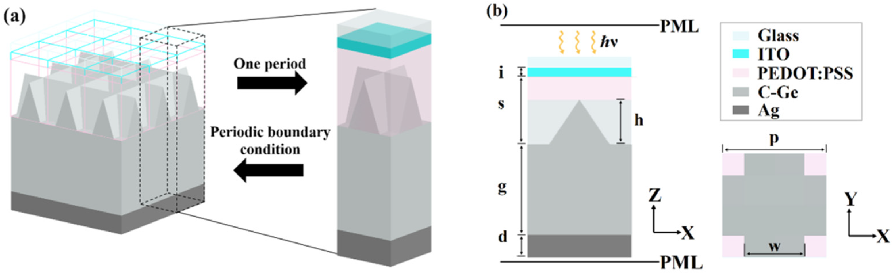
2. Structure and Method

In this paper, the finite-difference time-domain (FDTD) method was used to calculate the device, and the FDTD solution software (Lumerical FDTD Solutions 8.15) was used for building model and simulating the device [32,33]. The simulation 3D model and material distribution of each layer are shown in Figure 1. Ge was used as the absorber layer, and the absorber layer was constructed with a periodically arranged CC structure. Based on the finite-difference time-domain method, the real sunlight exposure under AM1.5 was simulated, and its optical performance was analyzed. Simulation of real battery electrical performance was based on Maxwell’s electromagnetic theory.
The top layer of the device adopts the planar structure of silicon dioxide (SiO2) transparent glass; with a thickness of 80 nm, its structure can effectively reduce the reflection loss so that more light gets through to the absorption layer and plays the role of passivation protection. The second layer of planar structure is indium tin oxide (ITO) with a thickness of 80 nm, which has the advantages of high transmittance and good electrical conductivity. It can be used as the top electrode layer so the incident light does not block when entering the absorption layer and reduces the recombination loss. The third layer is a planar organic hole transport layer composed of poly(3,4-ethylenedioxythiophene):poly(styrenesulfonate) (PEDOT:PSS), with a thickness of 600 nm, which can effectively block electrons [34], improve the hole transport efficiency and reduce the direct recombination of carriers [35]. Fourth layer for the absorption layer, with a height of 400 nm and width of 140 nm, is the cross cone of germanium nanostructures; it can effectively increase the light in the optical path absorbing layer, enhancing the absorption effect. Moreover, when the electromagnetic wave is incident on the metal or a highly doped semiconductor, the surface electrons in the material will be collectively oscillated, which will be converted into surface plasmon. This converts part of the light energy into electron collective oscillation energy on the surface of the material, making the light energy more easily absorbed by the material [36], so Ge material was selected as the nanostructure material. The fifth layer is germanium substrate with a thickness of 800 nm, which can improve the efficiency of electron transport and enhance the efficiency of light absorption. The sixth layer is the silver (Ag) electrode layer with a thickness of 200 nm, which has the advantages of high reflectance and high conductivity. It cannot only conduct electricity as an electrode but also reflects the unabsorbed light back to the absorption layer to improve the absorption rate. The lateral dimension of the solar cell model is designed to be 240 nm for a repeated cycle.
The device is provided with frequency domain power monitors on the upper and lower surfaces. The principle of the frequency domain power monitor is to sample in a certain frequency domain range and calculate the electric field (E) and the electric field passing through the surface at this frequency for each frequency sampling point. The magnetic field (H) is converted into the energy flux density (S, poynting vector), so that the whole area fraction will get the electromagnetic power passing through the whole surface. Among them, the frequency domain power monitor performs the interactive analysis of the frequency domain and the time domain through the standard Fourier transform, which can be expressed as [37]:
S = 1 μ 0 E × B  
Here μ0 is the vacuum permeability constant, and B is the magnetic induction intensity. It can be calculated by μ0H. From the energy flow density, the total energy of the system can be calculated by integrating over the whole closed space [38]:
W = Ω S × d σ  
Here   Ω   is a closed surface enclosed by the whole space, σ is an area vector, d σ is an area element, and W is the total energy of the system. After obtaining the electromagnetic power on the upper and lower surfaces of the device, the reflectivity and transmittance of the device can be analyzed. After the light enters the device from above the device, the reflected light is captured by the frequency domain power monitor on the upper surface, and the energy loss reflected by the device is calculated. Similarly, a monitor on the lower surface will capture and calculate the energy loss projected by the device. As the boundary conditions in the front, back, left and right directions of the device are selected as periodic boundary conditions, the scattered energy will be reabsorbed by the absorbing layer or become part of the reflection loss and projection loss and be captured by the frequency domain power monitor, so there is no additional calculation of the scattered energy. The optical absorption efficiency (A) of the device can be obtained through the reflectance efficiency (R) and transmission efficiency (T) [39,40,41,42,43]:
A = 1 R T
The evaluation indexes of solar cells include short-circuit current (ISC), open-circuit voltage (VOC), output power (P), filling factor (FF) and photoelectric conversion efficiency (η) [44]. ISC is the current generated by the cell when only one wire connects the positive and negative ends of the cell, and the short-circuit current density (JSC) is ISC flowing through a unit area. VOC is the voltage at both ends of the battery when the external resistance value of the battery is infinite. P is the product of battery voltage and current, and its value nonlinearly varies with the change in external resistance, and its maximum value is the maximum output power (PMAX). FF represents the characteristics of PMAX that the solar cell can output with the optimal load, and its value is given by the following equation [45]:
E F = V OC ln ( V OC + 0.72 ) V OC + 1 × 100 %
η refers to the ratio of the output charge energy of a solar cell to the total input of solar energy, which is an important parameter to measure the quality and technical level of a cell, and its value is given by the following equation [46]:
η = P MAX S A M 1.5 × 100 %
Here S A M 1.5 is the incident power of solar cell device simulation, and its value is 100 mW/cm2. The finite-difference time-domain method is known as the Yee grid space discretization method. The method is directly solved in the time domain by transforming the Maxwell curl equation into a finite-difference formula. The electric and magnetic fields are alternately computed in the interwoven grid space by establishing a time-discrete progressive sequence. The difference scheme contains the parameters of the medium and can simulate various complex structures only by giving the corresponding parameters to each grid. It is one of the important methods for numerical calculation of electromagnetic fields [47].
In terms of optical simulation calculation and measurement, we used FDTD solutions software for modeling and numerical calculation and set up geometric parameters, boundary conditions, positions of various monitors and light sources. A set of parameters were determined, and the obtained spectra were analyzed and optimized to achieve the best light absorption effect in the visible range. Then, the distribution and intensity of the electromagnetic field and the current density were calculated. In terms of electrical simulation calculation and measurement, after modeling with the Lumerical DEVICE software (Lumerical Suite 2018), the open-circuit voltage, short-circuit current, electrical power, reverse saturation current and photoelectric conversion efficiency were calculated to explore the influence of parameters on the data.

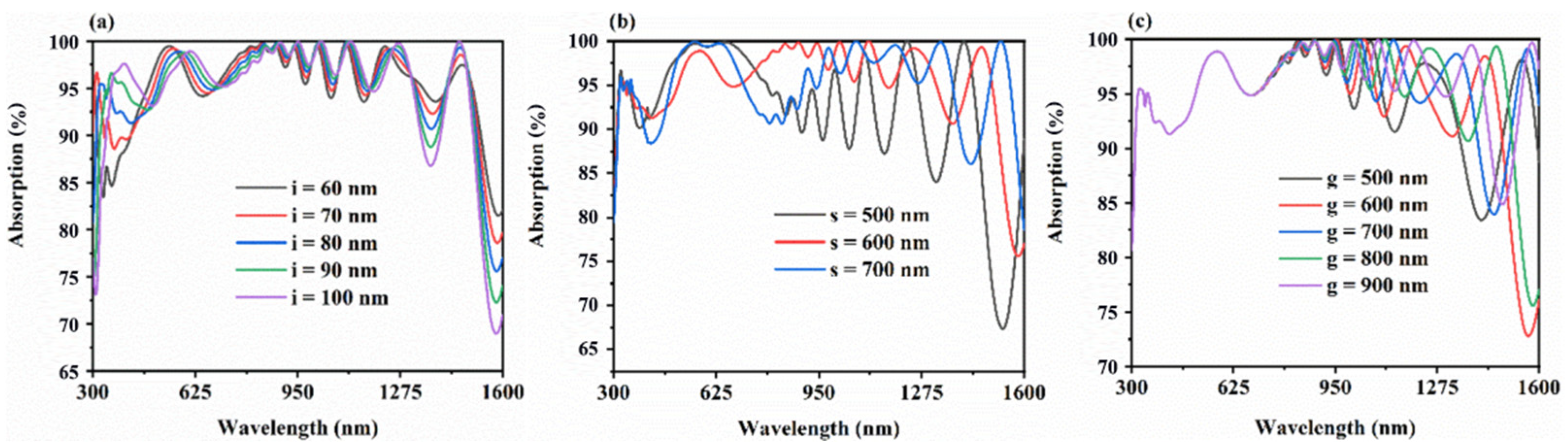
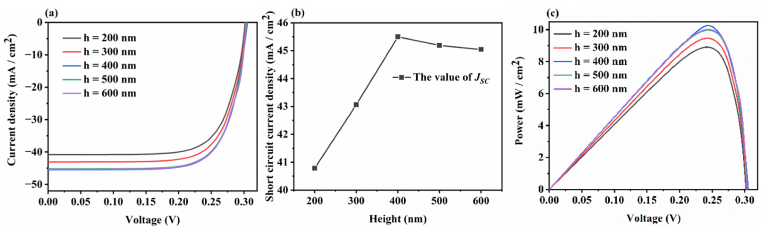
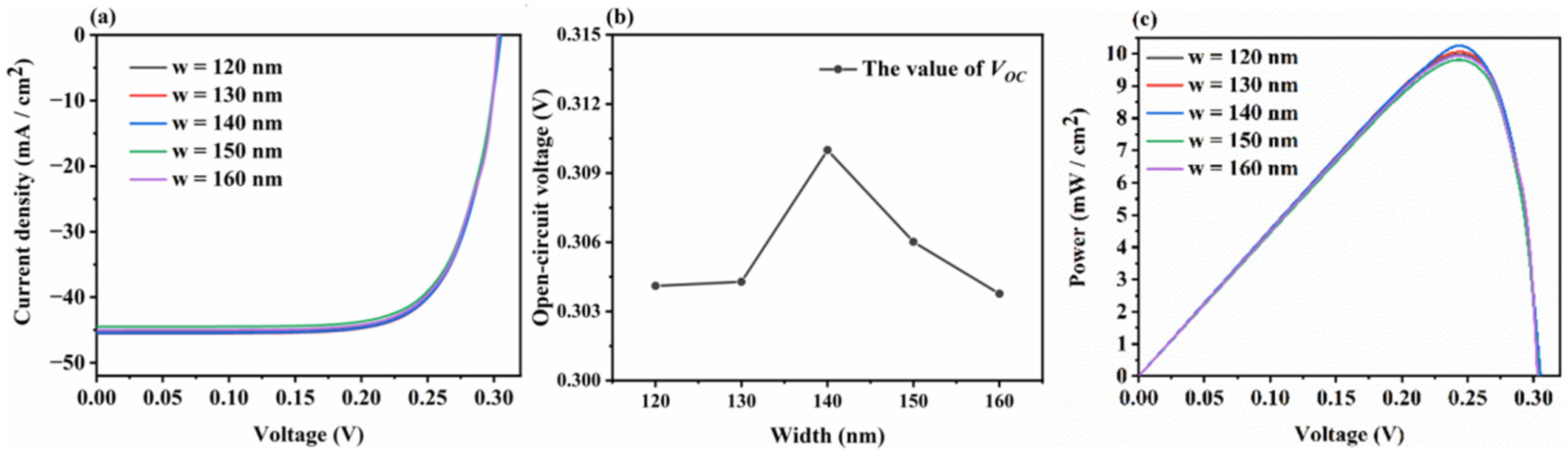
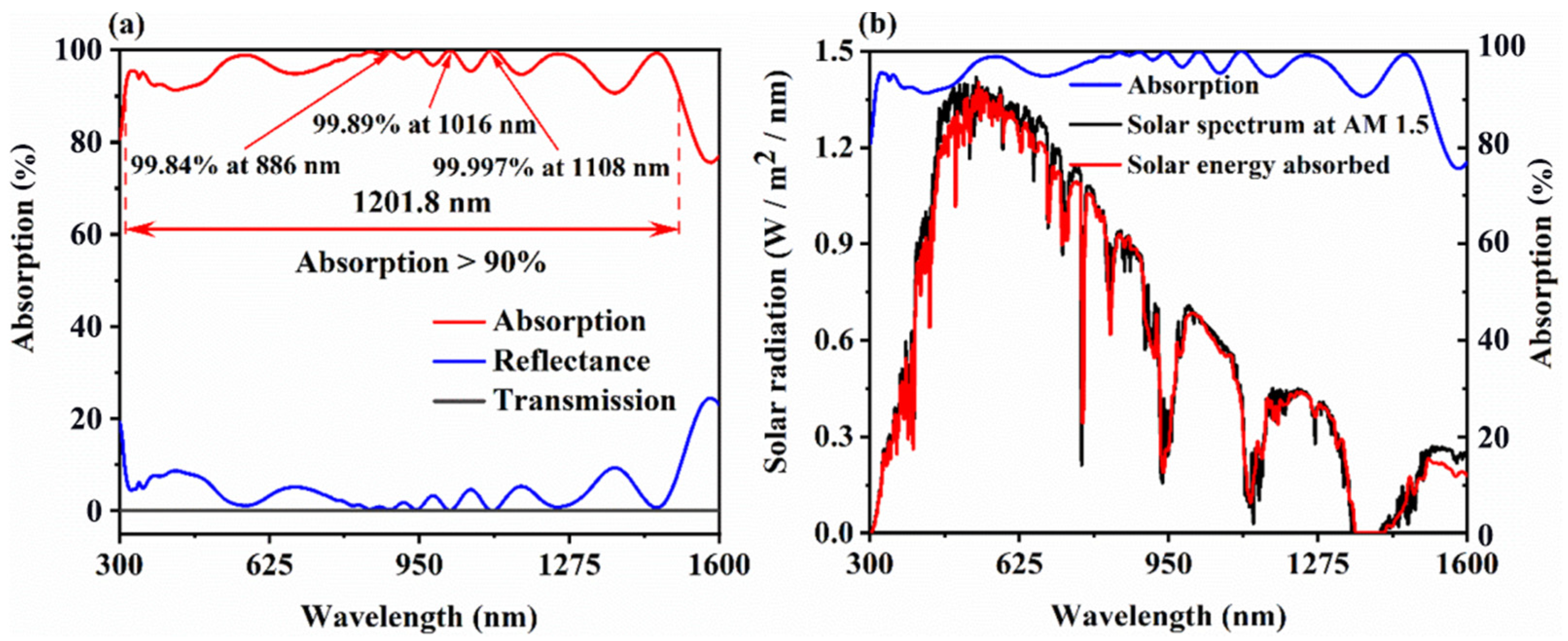
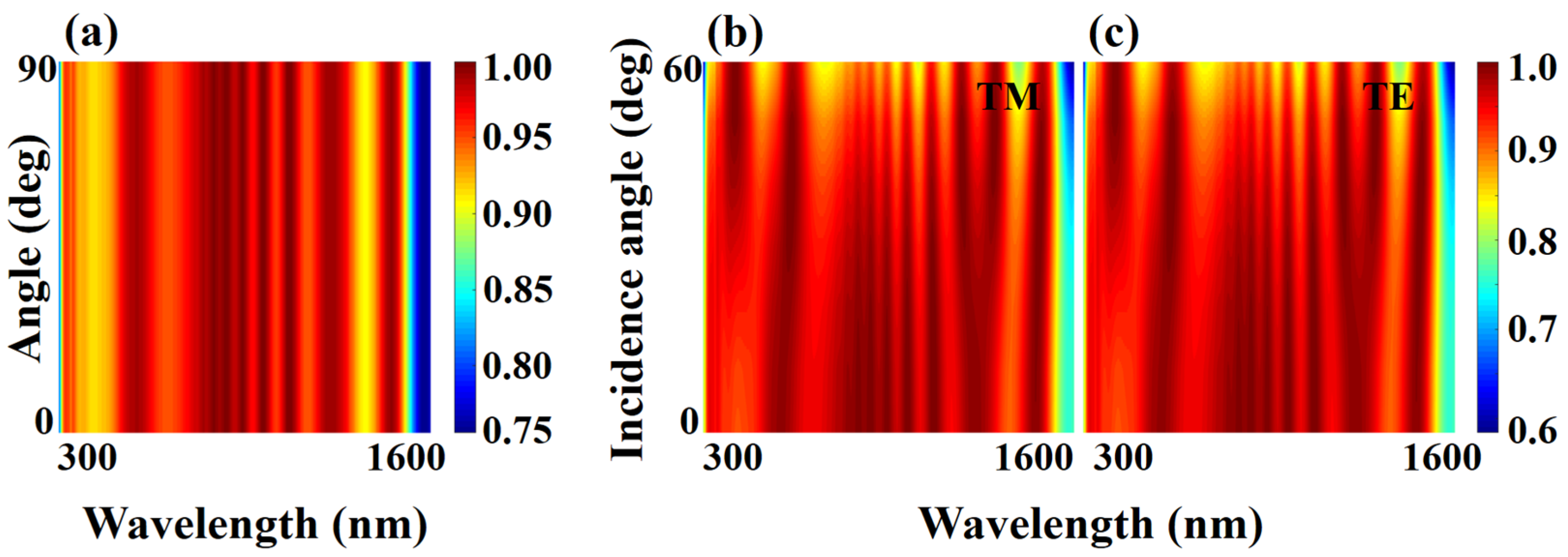
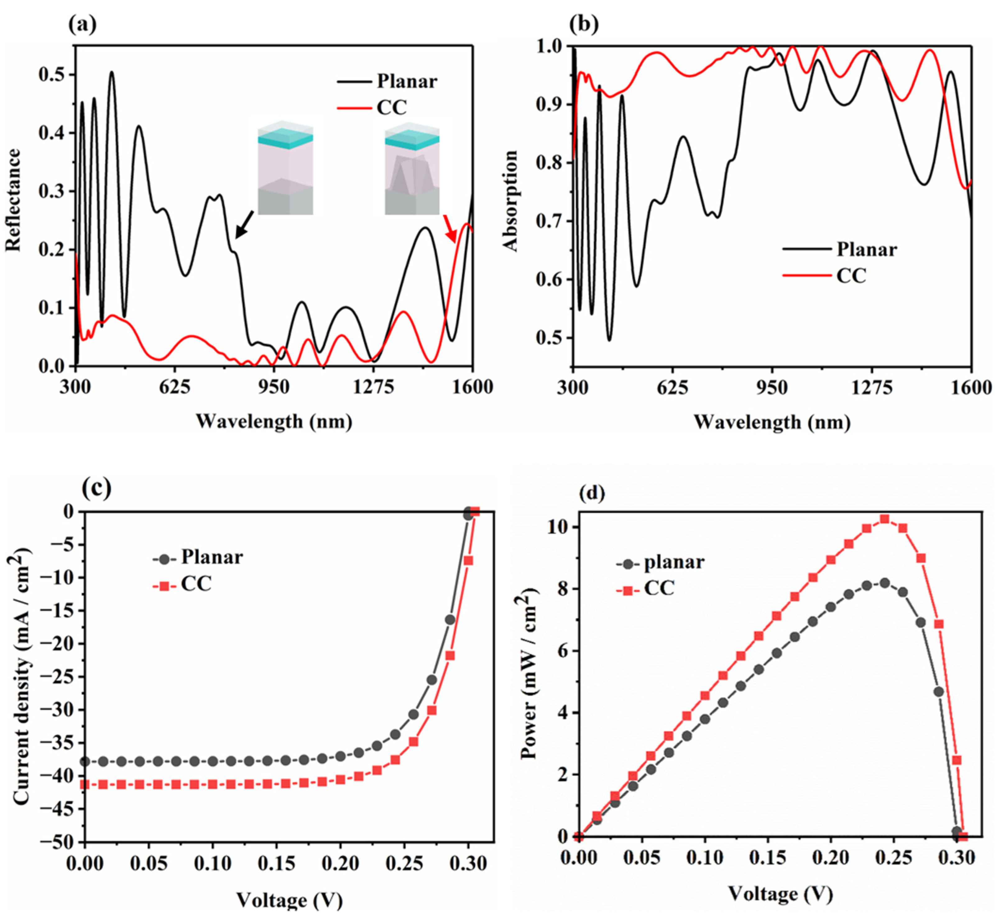
3. Results and Discussion

Figure 2a shows the effect of the ITO thickness of the conductive glass on the absorptivity. It can be seen from the figure that when the thickness of the ITO layer is 60 nm, the absorption in the near-ultraviolet and visible light bands decreases, and when the light wavelength is less than 500 nm, the light absorption efficiency is significantly reduced. As the thickness of the ITO layer is gradually increased, the light absorption spectrum of the device undergoes a slight redshift, the light absorption efficiency in the visible light band is slightly enhanced, and the light absorption in the near-ultraviolet band is significantly enhanced. However, the absorption efficiency in the near-infrared band greatly fluctuates. When the thickness of the ITO layer reaches 100 nm, the two absorption valleys in the near-infrared band significantly sink, and the light absorption of one absorption peak reaches the absorption efficiency of 99%, and the overall absorption efficiency is still reduced. In addition, the light absorption efficiency at the light wavelength of 1371.9 nm is <90%, which narrows the wavelength range of the perfect absorption (light absorption > 90%) [48,49] of the device. When the thickness of the ITO layer is 80 nm, it shows a good absorption efficiency in the near-ultraviolet, visible light, and near-infrared as a whole. At the same time, the light absorption efficiency at the light wavelength of 1371.9 nm reaches 90.7%, which broadens the range of the perfect absorption (light absorption > 90%) of the device to a wavelength width of 1201 nm. Therefore, the ITO layer thickness of 80 nm is a relatively good structural parameter.
As can be seen from Figure 2b, after increasing the thickness of the organic layer of PEDOT:PSS, the light absorption spectrum of the device exhibits an obvious redshift phenomenon because the light with a longer wavelength passes through the organic layer more easily to reach the nanostructured absorption layer [50]. When the thickness of the organic layer is 500 nm, the absorption effect in the visible light band is the best, but the absorption variation in the infrared band greatly fluctuates, and the six absorption valleys within 780–1600 nm are all less than 90% of the light absorption efficiency, and the overall absorption effect is not good. When the thickness of the organic layer increases to 700 nm, the absorption efficiency significantly decreases in the light wavelength range of 400–500 nm and 800–900 nm due to the increase in the hole transport path, and the absorption efficiency at the wavelength of 1430 nm is 86.1%, which is still less than 90%. When the thickness of the organic layer of the device is set to 600 nm, the original absorption valley moves to 1372 nm, and the absorption efficiency reaches 90.7%, which broadens the range of the perfect absorption (light absorption > 90%) of the device, and at the subthickness, the light absorption in the visible light band does not significantly decrease, which is within an acceptable range. Therefore, a thickness of 600 nm for the organic layer of PEDOT:PSS is a relatively optimal structural parameter.
It can be seen from Figure 2c that the thickness of the Ge absorption layer has little effect on the visible light because the thickness of the Ge base is larger than the wavelength of the visible light, and the visible light and near-ultraviolet light can hardly penetrate the Ge base. When the thickness increases, the visible light and near-ultraviolet light are still unable to pass through. For near-infrared light, as the thickness of the Ge base layer increases, the wavelength range of the light that can be transmitted is reduced, so the light absorption of the entire wavelength band is enhanced to a certain extent [51,52]. From Figure 2c, it can be seen that when the thickness of the Ge base layer is 600 nm and 800 nm, there is better light absorption in the near-infrared band, while the absorption peaks and troughs with a thickness of 800 nm are higher than those with a thickness of 600 nm except for the light wavelengths of 1371 nm and 1251 nm. Therefore, the thickness of 800 nm is a relatively good structural parameter for the Ge base layer.
It can be seen from Figure 3a that when the cross-cone height is 400 nm, the short-circuit current (Isc), VOC, and the output power is better than the other curves. The JSC was analyzed, as shown in Figure 3b, and it was found that the JSC of 45.5 mA/cm2 with a cross-cone height of 400 nm was 0.4 mA/cm2 higher than that of 500 nm of 45.1 mA/cm2. At the same time, the VOC of the CC structure with a height of 400 nm reaches 0.31 V, so the CC with a height of 400 nm has better electrical characteristics.
Figure 3c is the output power curve of the model. It was found that the output power of the cross-cone height of 400 nm is higher than other parameters, and the PMAX is 0.4 mW/cm2 higher than other parameters, subdivided into 400 nm and 600 nm. When the cross-cone height is 400 nm, the PMAX is 10.3 mW/cm2, and the PMAX at 600 nm is 9.9 mW/cm2. In conclusion, the CC height of 400 nm is a relatively optimal structural parameter for the device.
When the optimal cross-cone height is fixed and the bottom width is increased, the slope of the cross cone is indirectly changed. For the absorption layer of the device, that is, the CC structure, the most important variables are the slope and height. Therefore, for the slope of the cross cone, five variable values were set as test samples in this experiment, ranging from 120 to 160 nm, respectively, to observe its influence on the current density, VOC and output power of the device. As shown in Figure 4a, it was found that the slope of the cross cone has little effect on the ISC, and the maximum is 45.5 mA/cm2 at 140 nm. However, after changing the width of the cross cone, the VOC has a peak value, as shown in Figure 4b. When the width of the cross cone is 140 nm, the VOC of the device reaches the maximum value of 0.31 V.
The CC width of 140 nm is not only the result of the local optimal VOC but also the index performance of the JSC, which is not bad; for the output power, it also exceeds the index value of other variable values [53]. As can be seen from Figure 4c, when the width of the cross cone is 140 nm, its output power is higher than the other curves, and its PMAX reaches 10.3 mW/cm2, while the PMAX at 150 nm is 9.8 mW/cm2. It can be concluded that the CC width of 140 nm is a relatively optimal structural parameter for the device.
After the modeling and parameter optimization of the FDTD solutions of the device, the reflection loss, projection loss and light absorption efficiency of the device in the wavelength range of 300–1600 nm were analyzed. From Figure 5a, it can be seen that the device has good optical properties in the investigated light wavelength range (300–1600 nm). Due to the thickness of the Ge base layer and the reflective properties of the underlying silver, light in the visible and near-infrared bands is almost impermeable to the device, and its transmittance is almost constant over the entire study wavelength range [54,55,56]. As for the absorption rate, within 300–1600 nm, the average light absorption rate of the device under AM1.5G is 94.6%, and in the light wavelength range from 310 nm to 1512 nm with a width of 1201 nm, the absorption rate is greater than 90%, which is in line with the high absorption of the broadband. Among them, the absorption rate at 886 nm reaches 99.84%, the absorption rate at 1016 nm reaches 99.89%, and the absorption rate at 1108 nm reaches 99.997%, which is close to full absorption; a single absorber can be well-used in the field of sensing and detection.
In order to better restore the solar radiation on the surface under real conditions and simulate the sunlight absorption of this device, the simulation of this device adopted the international standard solar spectrum line air mass 1.5 (AM1.5). AM1.5 is the average illuminance of sunlight reaching the surface. The total irradiance of sunlight under its standard is 100 mW/cm2, which is divided into AM1.5G (global) and AM1.5D (direct) [46]. Due to the existence of the atmosphere on the earth, when the sunlight enters the atmosphere, it not only transmits light but also produces reflection and scattering. When the sun is obliquely incident in the morning or afternoon, the atmosphere that needs to pass through is thicker, and the intensity of the scattered light is higher. In addition, as there are objects with unevenness and shapes on the surface, when light is incident on the object, reflection and scattering will also occur [57,58,59]. Therefore, the sunlight received by any object on the surface is not only the direct sunlight but also the superposition of various reflected light and scattered light. AM1.5G includes this reflected and scattered light. As can be seen from Figure 5b, the device fits well with the AM1.5G solar spectrum and exhibits a good light absorption performance.
Sunlight belongs to natural light, which is the superposition of countless polarized lights in different directions. Therefore, the polarization state of light is also an influencing factor for most solar cells [60,61]. Based on this, this experiment explored the influence of different polarization states on the device. Take the polarization state of the incident light as a variable, change different polarization states to calculate the light absorption under the current polarization state, take the wavelength and polarization angle as the X-axis and Y-axis and the corresponding light absorption rate as the Z-axis, import the data obtained from the simulation into MATLAB, draw a heat map and get Figure 6a. It can be seen that when the wavelength is fixed, the polarization angle has no effect on the light absorption of the device, and the device exhibits good antipolarization properties.
In the real situation of the surface of the earth, the sun always rises in the east and sets in the west, and the sunlight on the solar cell experiences grazing incidence, oblique incidence, and normal incidence, respectively, and then reverses from normal incidence to grazing incidence in the afternoon, and finally, there is no light. In addition, as the latitude is different, the angle of sunlight irradiation is also different. At most times of the day, the illumination state of the solar cell belongs to the oblique incidence with an incident angle of less than 60°, so the incident angle of sunlight is an important factor affecting the light absorption of solar cells [62,63,64]. This experiment additionally used the incident angle of light as a variable for the TE mode (the direction of the electric field is perpendicular to the propagation direction) and the TM mode (the direction of the magnetic field is perpendicular to the propagation direction) to explore the effect of the incident angle on the light absorption of the device, respectively, taking the wavelength and incident angle as the X-axis and the Y-axis and the light absorption rate as the Z-axis and importing the obtained simulation data into MATLAB to make a heat map. The results are shown in Figure 6b,c. When the incident angle of the incident light is located at 0–60°, the device can ensure that the light absorption within 300–1500 nm is greater than 80% and has good angle tolerance.
In order to explore the influence of the nanostructures and corrugation on the light absorption of solar cells, this experiment simulated and compared the absorption layer with a cross-cone structure (CC) and a planar structure and calculated its reflectance and absorptivity, as shown in Figure 7a,b. It can be seen from the two figures that if the nanostructure absorption layer is not provided, the overall reflectivity of the device is significantly increased, and the corresponding absorption rate is significantly reduced, so the light absorption efficiency of the solar cell is not high. After adding the nanoperiodic arrangement of the CC structure, the light absorption effect of the device is significantly improved. Depending on the shape of the nanostructure, light is reflected multiple times in it, increasing the optical path inside the device, and the energy of the light is constantly attenuated, absorbed by the electrons in the absorption layer [57] and forms a potential difference under the action of the PN junction, which is converted into electrical energy. Therefore, the CC structure can effectively improve the light absorption effect of the solar device.
Figure 7c,d shows the influence of the nanostructure on the circuit current and output power of the designed device. The devices obtained in this study have good electrical properties. The VOC of the germanium-based solar cells under the single-junction CC nanostructure absorber structure array is 0.31 V, and the JSC reaches 45.5 mA/cm2. The FF value of the device can be calculated as 72.7% by Equation (4). The η of the device of 10.3% can be reached by Equation (5). Compared with recent studies on single-junction silicon solar cells [58], the JSC of the Ge-based solar cells increases from 42.6 mA/cm2 to 45.5 mA/cm2, the weighted absorption efficiency at AM1.5G improves from 91.66% to 94.6%, and the thickness improves from 101 um to 1.8 um. Table 1 shows the performance comparison of the germanium-based solar cells under the CC nanostructure absorber structure array designed in this paper with other Ge solar cells of the same type [10,19,65,66,67], which have excellent competitiveness and market application potential.

4. Conclusions

In this paper, using Ge as the substrate, a solar cell with a Ge cross-cone nanostructure as the absorber layer was designed with a thickness of only 1.8 μm. The structure optimization and model numerical simulation were carried out separately under optical and electrical conditions. In terms of optics, due to the reflection caused by the Ge cross-cone nanostructure array, the light transmission distance of the absorption layer increased, and the electromagnetic wave irradiated the metal surface to generate surface plasmons to enhance the light absorption. After the optimization of the structural parameters of the device, the real simulation of AM1.5G was carried out to ensure the stable operation of the actual situation. Under the optimal structural parameters, its average weighted absorption rate from 300 nm to 1600 nm was 94.6%. At the same time, the perfect absorption band of the device (the band with light absorption > 90%) reached 1201 nm, and the absorption rate at 1108 nm reached 99.997%, which is close to complete absorption. At the same time, the effects of the incident angle and polarization angle on the light absorption of the device were also explored, and the polarization and angle tolerance of the germanium-based solar cells under the nanocross-cone absorbing structure array were verified. From an electrical aspect, the influence of the cross-conical nanostructure array of Ge material as the absorber layer on the electrical properties of the device was explored by analyzing the performance of each variable, one by one, after the simulation, and the optimal configuration ratio and parameters of the cross-cone nanostructure of Ge material were obtained. Through the analysis, the VOC and JSC of the optimal performance device were 0.31 V and 45.5 mA/cm2, achieving a photoelectric conversion efficiency of 10.3% and a high FF of 72.7%, surpassing the performance of most Ge solar cells today.

Author Contributions

Conceptualization, Z.Z., and W.L.; data curation, Z.Z., Y.G. and H.H.; formal analysis, Z.Z. and X.D.; methodology, Z.Z., W.L., Y.G. and X.D.; resources, Y.G.; software, Z.Z., W.L., H.H. and X.D.; data curation, Z.Z.; writing—original draft preparation, Z.Z.; writing—review and editing, Z.Z., W.L., H.H. and X.D. All authors have read and agreed to the published version of the manuscript.

Funding

The authors are grateful to the support by the Scientific Research Fund of Zhejiang Provincial Education Department (Y202146019).

Institutional Review Board Statement

Not applicable.

Informed Consent Statement

Not applicable.

Data Availability Statement

Publicly available datasets were analyzed in this study. This data can be found here: https://www.lumerical.com/ (accessed on 24 October 2020).

Conflicts of Interest

The authors declare no conflict of interest.

References

  1. Rabeh, A.; Abdelkader, A.; Mohamed, J.; Souad, C. Identification of unknown parameters of solar cell models: A comprehensive overview of available approaches. Renew. Sustain. Energy Rev. 2018, 90, 453–474. [Google Scholar] [CrossRef]
  2. Agnihotri, S.; Samajdar, D.P. Design of InP-based truncated nanopyramid solar cells with conformal coating of PEDOT PSS for improved light harvesting efficiency. Opt. Mater. 2020, 110, 110475. [Google Scholar] [CrossRef]
  3. Zhao, F.; Lin, J.; Lei, Z.; Yi, Z.; Qin, F.; Zhang, J.; Liu, L.; Wu, X.; Yang, W.; Wu, P. Realization of 18.97% theoretical efficiency of 0.9 μm thick c-Si/ZnO heterojunction ultrathin-film solar cells via surface plasmon resonance enhancement. Phys. Chem. Chem. Phys. 2022, 24, 4871–4880. [Google Scholar] [CrossRef] [PubMed]
  4. Zhou, F.; Qin, F.; Yi, Z.; Yao, W.-T.; Liu, Z.; Wu, X.; Wu, P. Ultra-wideband and wide-angle perfect solar energy absorber based on Ti nanorings surface plasmon resonance. Phys. Chem. Chem. Phys. 2021, 23, 17041–17048. [Google Scholar] [CrossRef] [PubMed]
  5. Li, Y.; Li, M.; Xu, P.; Tang, S.; Liu, C. Efficient photocatalytic degradation of acid orange 7 over N-doped ordered mesoporous titania on carbon fibers under visible-light irradiation based on three synergistic effects. Appl. Catal. A Gen. 2016, 524, 163–172. [Google Scholar] [CrossRef]
  6. Xiao, L.; Zhang, Q.I.; Chen, P.; Chen, L.; Ding, F.; Tang, J.; Li, Y.J.; Au, C.T.; Yin, S.F. Copper-mediated metal-organic framework as efficient photocatalyst for the partial oxidation of aromatic alcohols under visible-light irradiation: Synergism of plasmonic effect and schottky junction. Appl. Catal. B-Environ. 2019, 248, 380–387. [Google Scholar] [CrossRef]
  7. Luo, W.H.; Cao, W.X.; Bruijnincx, P.C.A.; Lin, L.; Wang, A.Q.; Zhang, T. Zeolite-supported metal catalysts for selective hydrodeoxygenation of biomass-derived platform molecules. Green Chem. 2019, 21, 3744–3768. [Google Scholar] [CrossRef]
  8. Lin, X.; Li, Y.J.; Chen, F.T.; Xu, P.; Li, M. Facile synthesis of mesoporous titanium dioxide doped by Ag-coated graphene with enhanced visible-light photocatalytic performance for methylene blue degradation. RSC Adv. 2017, 7, 25314–25324. [Google Scholar] [CrossRef] [Green Version]
  9. Sukeerthi, M.; Kotamraju, S. Trap and carrier removal study of 4J InGaP/InGaAs-GaAsP MQW/InGaAsNSb/Ge high efficient space solar cell using advanced physical models. Phys. E Low-Dimens. Syst. Nanostruct. 2021, 134, 114914. [Google Scholar] [CrossRef]
  10. Zhao, F.; Chen, X.; Yi, Z.; Qin, F.; Tang, Y.J.; Yao, W.T.; Zhou, Z.G.; Yi, Y.G. Study on the solar energy absorption of hybrid solar cells with trapezoid-pyramidal structure based PEDOT:PSS/c-Ge. Sol. Energy 2020, 204, 635–643. [Google Scholar] [CrossRef]
  11. Prieto, I.; Galiana, B.; Postigo, P.A. Enhanced quantum efficiency of Ge solar cells by a two-dimensional photonic crystal nanostructured surface. Appl. Phys. Lett. 2009, 94, 191102. [Google Scholar] [CrossRef] [Green Version]
  12. Masuda, T.; Faucher, J.; Lee, M.L. Molecular beam epitaxy growth of germanium junctions for multi-junction solar cell applications. J. Phys. D Appl. Phys. 2016, 49, 465105. [Google Scholar] [CrossRef]
  13. Baran, V.; Cat, Y.; Sertel, T.; Ataser, T.; Sonmez, N.A.; Cakmak, M.; Ozcelik, S. A comprehensive study on a stand-alone germanium (Ge) solar cell. J. Electron. Mater. 2020, 49, 1249–1256. [Google Scholar] [CrossRef]
  14. Lombardero, I.; Cifuentes, L.; Gabás, M.; Algora, C. Manufacturing process for III–V multijunction solar cells on germanium substrates with a total thickness below 60 microns. Prog. Photovolt. Res. Appl. 2022, 30, 740–749. [Google Scholar] [CrossRef]
  15. Sharma, T.; Mahajan, P.; Adil, A.M.; Singh, A.; Yukta, T.N.K.; Purohit, S.; Verma, S.; Padha, B.; Gupta, V.; Arya, S.; et al. Recent Progress in Advanced Organic Photovoltaics: Emerging Techniques and Materials. ChemSusChem 2022, 15, e202101067. [Google Scholar] [CrossRef]
  16. William, M.A.; Azhari, A.W.; Hassan, N.; Hasan, N.; Halin, D.; Thottoli, A.K. Absorption study on the effect of mixed cation on tin and germanium-based perovskite solar cells. IOP Conf. Ser. Earth Environ. Sci. 2021, 920, 012032. [Google Scholar] [CrossRef]
  17. Meng, X.; Tang, T.; Zhang, R.; Liu, K.Y.; Li, W.H.; Yang, L.; Song, Y.B.; Ma, X.X.; Cheng, Z.H.; Wu, J. Optimization of germanium-based perovskite solar cells by SCAPS simulation. Opt. Mater. 2022, 128, 112427. [Google Scholar] [CrossRef]
  18. Tian, X.; Yun, H.C.; Hui, T.F.; Yan, M.S. Optimal bulk-heterojunction morphology enabled by fibril network strategy for high-performance organic solar cells. Sci. China Chem. 2019, 62, 662–668. [Google Scholar] [CrossRef]
  19. Nakano, S.; Shiratani, M. Impact of heterointerface properties of crystalline germanium heterojunction solar cells. Thin Solid Film. 2019, 685, 225–233. [Google Scholar] [CrossRef]
  20. Zheng, Z.; Luo, Y.; Yang, H.; Yi, Z.; Zhang, J.; Song, Q.; Yang, W.; Liu, C.; Wu, X.; Wu, P. Thermal tuning of terahertz metamaterial properties based on phase change material vanadium dioxide. Phys. Chem. Chem. Phys. 2022, 24, 8846–8853. [Google Scholar] [CrossRef]
  21. Zheng, Z.; Zheng, Y.; Luo, Y.; Yi, Z.; Zhang, J.; Liu, Z.; Yang, W.; Yu, Y.; Wu, X.; Wu, P. A switchable terahertz device combining ultra-wideband absorption and ultra-wideband complete reflection. Phys. Chem. Chem. Phys. 2022, 24, 2527–2533. [Google Scholar] [CrossRef] [PubMed]
  22. Gu, Y.F.; Guo, B.B.; Yi, Z.; Wu, X.W.; Zhang, J.; Yang, H. Morphology modulation of hollow-shell ZnSn(OH)6 for enhanced photodegradation of methylene blue. Colloids Surf. A Physicochem. Eng. Asp. 2022, 653, 129908. [Google Scholar] [CrossRef]
  23. Cheng, T.; Gao, H.; Liu, G.; Pu, Z.; Wang, S.; Yi, Z.; Wu, X.; Yang, H. Preparation of core-shell heterojunction photocatalysts by coating CdS nanoparticles onto Bi4Ti3O12 hierarchical microspheres and their photocatalytic removal of organic pollutants and Cr(VI) ions. Colloids Surf. A Physicochem. Eng. Asp. 2021, 633, 127918. [Google Scholar] [CrossRef]
  24. Li, L.; Gao, H.; Liu, G.; Wang, S.; Yi, Z.; Wu, X.; Yang, H. Synthesis of carnation flower-like Bi2O2CO3 photocatalyst and its promising application for photoreduction of Cr(VI). Adv. Powder Technol. 2022, 33, 103481. [Google Scholar] [CrossRef]
  25. Li, J.; Jiang, J.; Zhao, D.; Xu, Z.; Liu, M.; Liu, X.; Tong, H.; Qian, D. Novel hierarchical sea urchin-like Prussian blue@palladium core–shell heterostructures supported on nitrogen-doped reduced graphene oxide: Facile synthesis and excellent guanine sensing performance. Electrochim. Acta 2020, 330, 135196. [Google Scholar] [CrossRef]
  26. Cao, W.X.; Lin, L.; Qi, H.F.; He, Q.; Wu, Z.J.; Wang, A.Q.; Luo, W.H.; Zhang, T. In-situ synthesis of single-atom Ir by utilizing metal-organic frameworks: An acid-resistant catalyst for hydrogenation of levulinic acid to gamma-valerolactone. J. Catal. 2019, 373, 161–172. [Google Scholar] [CrossRef] [Green Version]
  27. Lin, X.; Li, M.; Li, Y.J.; Chen, W. Enhancement of the catalytic activity of ordered mesoporous TiO2 by using carbon fiber support and appropriate evaluation of synergy between surface adsorption and photocatalysis by Langmuir-Hinshelwood (L-H) integration equation. RSC Adv. 2015, 5, 105227–105238. [Google Scholar] [CrossRef]
  28. Liu, Y.; Bo, M.; Yang, X.; Zhang, P.; Sun, C.Q.; Huang, Y. Size modulation electronic and optical properties of phosphorene nanoribbons: DFT–BOLS approximation. Phys. Chem. Chem. Phys. 2017, 19, 5304–5309. [Google Scholar] [CrossRef]
  29. Mavrokefalos, A.; Han, S.E.; Yerci, S.; Branham, M.S.; Chen, G. Efficient Light Trapping in Inverted Nanopyramid Thin Crystalline Silicon Membranes for Solar Cell Applications. Nano Lett. 2012, 12, 2792–2796. [Google Scholar] [CrossRef]
  30. Chen, S.H.; Yeh, Y.W.; Tseng, S.Z.; Shih, I.T.; Chan, C.H.; Lee, C.C. Light harvesting analysis of a nano-cylinder structure on crystalline silicon using the Mie scattering model. J. Non-Cryst. Solids 2012, 358, 2214–2218. [Google Scholar] [CrossRef]
  31. Zhang, S.; Liu, M.; Liu, W.; Li, Z.; Liu, Y. High-efficiency photon capturing in ultrathin silicon solar cells with double-sided skewed nanopyramid arrays. J. Opt. 2017, 19, 105901. [Google Scholar] [CrossRef]
  32. Cao, G.; Li, H.; Deng, Y.; Zhan, S.; He, Z.; Li, B. Systematic Theoretical Analysis of Selective-Mode Plasmonic Filter Based on Aperture-Side-Coupled Slot Cavity. Plasmonics 2014, 9, 1163–1169. [Google Scholar] [CrossRef]
  33. Deng, Y.; Cao, G.; Yang, H.; Zhou, X.; Wu, Y. Dynamic Control of Double Plasmon-Induced Transparencies in Aperture-Coupled Waveguide-Cavity System. Plasmonics 2018, 13, 345–352. [Google Scholar] [CrossRef]
  34. Fei, M.; Yang, Z.; Li, J.H.; Xing, W.Z.; Haos, H.G.; Jing, B.Y. Nickel oxide for inverted structure perovskite solar cells. J. Energy Chem. 2021, 52, 393–411. [Google Scholar] [CrossRef]
  35. Mahajan, P.; Padha, B.; Verma, S.; Gupta, V.; Datt, R.; Tsoi, W.C.; Satapathi, S.; Arya, S. Review of current progress in hole-transporting materials for perovskite solar cells. J. Energy Chem. 2022, 68, 330–386. [Google Scholar] [CrossRef]
  36. Barnes, W.L.; Dereux, A.; Ebbesen, T.W. Surface plasmon subwavelength optics. Nature 2003, 424, 824–830. [Google Scholar] [CrossRef]
  37. Cai, L.; Zhang, Z.; Xiao, H.; Chen, S.; Fu, J. An eco-friendly imprinted polymer based on graphene quantum dots for fluorescent detection of p-nitroaniline. RSC Adv. 2019, 9, 41383–41391. [Google Scholar] [CrossRef] [Green Version]
  38. Mizanuzzaman, M.; Kader, M.F. Performance Evaluation of a Hybrid Photovoltaic Solar Thermal System. Am. J. Mech. Eng. 2020, 8, 154–162. [Google Scholar] [CrossRef]
  39. Wang, D.Y.; Yi, Z.; Ma, G.L.; Dai, B.; Yang, J.B.; Zhang, J.F.; Yu, Y.; Liu, C.; Wu, X.W.; Bian, Q. Two channels photonic crystal fiber based on surface plasmon resonance for magnetic field and temperature dual-parameter sensing. Phys. Chem. Chem. Phys. 2022, 24, 21233. [Google Scholar] [CrossRef]
  40. Gu, Y.F.; Guo, B.B.; Yi, Z.; Wu, X.W.; Zhang, J.; Yang, H. Synthesis of a Self-assembled Dual Morphologies Ag-NPs/SrMoO4 Photocatalyst with LSPR Effect for the Degradation of Methylene Blue Dye. ChemistrySelect 2022, 7, e202201274. [Google Scholar] [CrossRef]
  41. Li, L.; Gao, H.; Yi, Z.; Wang, S.; Wu, X.; Li, R.; Yang, H. Comparative investigation on synthesis, morphological tailoring and photocatalytic activities of Bi2O2CO3 nanostructures. Colloids Surf. A Physicochem. Eng. Asp. 2022, 644, 128758. [Google Scholar] [CrossRef]
  42. Liu, N.; Mesch, M.; Weiss, T.; Hentschel, M.; Giessen, H. Infrared perfect absorber and its application as plasmonic sensor. Nano Lett. 2010, 10, 2342–2348. [Google Scholar] [CrossRef] [PubMed]
  43. Chen, H.; Chen, Z.; Yang, H.; Wen, L.; Yi, Z.; Zhou, Z.; Dai, B.; Zhang, J.; Wu, X.; Wu, P. Multi-mode surface plasmon resonance absorber based on dart-type single-layer graphene. RSC Adv. 2022, 12, 7821–7829. [Google Scholar] [CrossRef] [PubMed]
  44. Qin, F.; Chen, X.; Yi, Z.; Yao, W.; Yang, H.; Tang, Y.; Yi, Y.; Li, H.; Yi, Y. Ultra-broadband and wide-angle perfect solar absorber based on TiN nanodisk and Ti thin film structure. Sol. Energy Mater. Sol. Cells 2020, 211, 110535. [Google Scholar] [CrossRef]
  45. Rajeev, P.P.; Ayyub, P.; Bagchi, S.; Kumar, G.R. Nanostructures, local fields, and enhanced absorption in intense light–matter interaction. Opt. Lett. 2004, 29, 2662–2664. [Google Scholar] [CrossRef]
  46. Bremner, S.P.; Levy, M.Y.; Honsberg, C.B. Analysis of tandem solar cell efficiencies under AM1. 5G spectrum using a rapid flux calculation method. Prog. Photovolt. Res. Appl. 2008, 16, 225–233. [Google Scholar] [CrossRef]
  47. Gulomov, J.; Aliev, R.; Mirzaalimov, A.; Mirzaalimov, N.; Kakhkhorov, J.; Rashidov, B.; Temirov, S. Studying the effect of light incidence angle on photoelectric parameters of solar cells by simulation. Int. J. Renew. Energy Dev. 2021, 10, 731–736. [Google Scholar] [CrossRef]
  48. Wu, X.; Zheng, Y.; Luo, Y.; Zhang, J.; Yi, Z.; Wu, X.; Cheng, S.; Yang, W.; Yu, Y.; Wu, P. A four-band and polarization-independent BDS-based tunable absorber with high refractive index sensitivity. Phys. Chem. Chem. Phys. 2021, 23, 26864–26873. [Google Scholar] [CrossRef]
  49. Chen, P.; Liu, F.; Ding, H.; Chen, S.; Chen, L.; Li, Y.-J.; Au, C.-T.; Yin, S.-F. Porous double-shell CdS@C3N4 octahedron derived by in situ supramolecular self-assembly for enhanced photocatalytic activity. Appl. Catal. B Environ. 2019, 252, 33–40. [Google Scholar] [CrossRef]
  50. Garnett, E.; Yang, P. Light Trapping in Silicon Nanowire Solar Cells. Nano Lett. 2010, 10, 1082–1087. [Google Scholar] [CrossRef]
  51. Ge, S.B.; Liu, W.G.; Zhou, S.; Li, S.J.; Sun, X.P.; Huang, Y.T.; Yang, P.F.; Zhang, J.; Lin, D.B. Design and Preparation of a Micro-Pyramid Structured Thin Film for Broadband Infrared Antireflection. Coatings 2018, 8, 192. [Google Scholar] [CrossRef] [Green Version]
  52. Li, J.; Jiang, J.; Xu, Z.; Liu, M.; Tang, S.; Yang, C.; Qian, D. Facile synthesis of Ag@Cu2O heterogeneous nanocrystals decorated N-doped reduced graphene oxide with enhanced electrocatalytic activity for ultrasensitive detection of H2O2. Sens. Actuators B Chem. 2018, 260, 529–540. [Google Scholar] [CrossRef]
  53. Cheng, Z.; Liao, J.; He, B.; Zhang, F.; Zhang, F.; Huang, X.; Zhou, L. One-Step Fabrication of Graphene Oxide Enhanced Magnetic Composite Gel for Highly Efficient Dye Adsorption and Catalysis. ACS Sustain. Chem. Eng. 2015, 3, 1677–1685. [Google Scholar] [CrossRef]
  54. Tang, N.; Li, Y.; Chen, F.; Han, Z. In situ fabrication of a direct Z-scheme photocatalyst by immobilizing CdS quantum dots in the channels of graphene-hybridized and supported mesoporous titanium nanocrystals for high photocatalytic performance under visible light. RSC Adv. 2018, 8, 42233–42245. [Google Scholar] [CrossRef] [Green Version]
  55. Zhang, Z.; Cai, R.; Long, F.; Wang, J. Development and application of tetrabromobisphenol A imprinted electrochemical sensor based on graphene/carbon nanotubes three-dimensional nanocomposites modified carbon electrode. Talanta 2015, 134, 435–442. [Google Scholar] [CrossRef]
  56. Lv, P.; Xie, D.; Zhang, Z. Magnetic carbon dots based molecularly imprinted polymers for fluorescent detection of bovine hemoglobin. Talanta 2018, 188, 145–151. [Google Scholar] [CrossRef]
  57. Li, L.; Sun, X.; Xian, T.; Gao, H.; Wang, S.; Yi, Z.; Wu, X.; Yang, H. Template-free synthesis of Bi2O2CO3 hierarchical nanotubes self-assembled from ordered nanoplates for promising photocatalytic applications. Phys. Chem. Chem. Phys. 2022, 24, 8279–8295. [Google Scholar] [CrossRef]
  58. Liu, H.; Wang, Q.; Zhang, F. Preparation of Fe3O4@SiO2@ P(AANa-co-AM) Composites and Their Adsorption for Pb(II). ACS Omega 2020, 5, 8816–8824. [Google Scholar] [CrossRef] [Green Version]
  59. Lin, X.; Du, S.W.; Li, C.H.; Li, G.J.; Li, Y.J.; Chen, F.T.; Fang, P.F. Consciously constructing the robust NiS/g-C3N4 hybrids for enhanced photocatalytic hydrogen evolution. Catal. Lett. 2020, 150, 1898–1908. [Google Scholar] [CrossRef]
  60. Shangguan, Q.Y.; Chen, Z.H.; Yang, H.; Cheng, S.B.; Yang, W.X.; Yi, Z.; Wu, X.W.; Wang, S.F.; Yi, Y.G.; Wu, P.H. Design of Ultra-Narrow Band Graphene Refractive Index Sensor. Sensors 2022, 22, 6483. [Google Scholar] [CrossRef]
  61. Zhang, C.; Yi, Y.T.; Yang, H.; Yi, Z.; Chen, X.F.; Zhou, Z.G.; Yi, Y.G.; Li, H.L.; Chen, J.; Liu, C. Wide spectrum solar energy absorption based on germanium plated ZnO nanorod arrays: Energy band regulation, Finite element simulation, Super hydrophilicity, Photothermal conversion. Appl. Mater. Today 2022, 28, 101531. [Google Scholar] [CrossRef]
  62. Long, F.; Wang, J.; Zhang, Z.; Yan, L. Magnetic imprinted electrochemical sensor combined with magnetic imprinted solid-phase extraction for rapid and sensitive detection of tetrabromobisphenol S. J. Electroanal. Chem. 2016, 777, 58–66. [Google Scholar] [CrossRef]
  63. Deng, Y.; Cao, G.; Wu, Y.; Zhou, X.; Liao, W. Theoretical Description of Dynamic Transmission Characteristics in MDM Waveguide Aperture-Side-Coupled with Ring Cavity. Plasmonics 2015, 10, 1537–1543. [Google Scholar] [CrossRef]
  64. Long, F.; Zhang, Z.; Wang, J.; Yan, L.; Zhou, B. Cobalt-nickel bimetallic nanoparticles decorated graphene sensitized imprinted electrochemical sensor for determination of octylphenol. Electrochim. Acta 2015, 168, 337–345. [Google Scholar] [CrossRef]
  65. Bahman, H.; Davood, S.; Marinus, H.; Keith, F.; Devendra, K.S. High-efficiency heterojunction solar cells on crystalline germanium substrates. Appl. Phys. Lett. 2012, 101, 032102. [Google Scholar] [CrossRef] [Green Version]
  66. Nakano, S.; Takeuchi, Y.; Kaneko, T.; Michio, K. Influence of surface treatments on crystalline germanium heterojunction solar cell characteristics. J. Non-Cryst. Solids 2012, 358, 2249–2252. [Google Scholar] [CrossRef]
  67. Onyegam, E.U.; Sarkar, D.; Hilali, M.; Saha, S.; Rao, R.A.; Mathew, L.; Jawarani, D.; Mantey, J.; Ainom, M.; Garcia, R.; et al. Exfoliated, thin, flexible germanium heterojunction solar cell with record FF=58.1%. Sol. Energy Mater. Sol. Cells 2013, 111, 206–211. [Google Scholar] [CrossRef]
Figure 1. (a) Germanium-based solar cell device under periodic arrangement. (b) 2D view and material composition of each layer. i is the thickness of the ITO layer, s is the thickness of PEDOT:PSS, g is the thickness of the substrate germanium, d is the thickness of the bottom silver electrode, h is the height of the germanium cross cone nanostructure, p is the width of the germanium nanostructure array in one period and w is the bottom width of the germanium cross cone nanostructure.
Coatings 12 01653 g001
Figure 2. (a) Influence of ITO thickness of conductive glass on absorptivity. (b) Influence of organic layer of PEDOT:PSS thickness on absorptivity. (c) Influence of Ge base layer thickness on absorptivity.
Coatings 12 01653 g002
Figure 3. (a) Current density curves at different cross-cone heights. (b) The effect of cross-cone heights on JSC. (c) Output power curves at different cross-cone heights.
Coatings 12 01653 g003
Figure 4. (a) J-V curve under different cross-cone widths. (b) Influence of cross-cone width on VOC. (c) Output power curve under different cross-cone widths.
Coatings 12 01653 g004
Figure 5. (a) Absorption, reflection and transmission of the device in the wavelength range of 300–1600. (b) Weighted absorption at AM1.5.
Coatings 12 01653 g005
Figure 6. (a) The effect of different polarized light on the optical absorption of the device. (b) The effect of different incident angles on the optical absorption of the device in TM mode. (c) The effect of different incident angles on the optical absorption of the device in TE mode.
Coatings 12 01653 g006
Figure 7. (a) The influence of the presence or absence of the CC nanostructure on the reflectivity. (b) The effect of the presence or absence of the CC nanostructure on the absorptivity. (c) The influence of the presence or absence of the CC nanostructure on the current density. (d) The influence of the presence or absence of the CC nanostructure on the output power.
Coatings 12 01653 g007
Table 1. Comparison of performance of different Ge micro-nanostructured solar cells.
ReferencesPerfect Absorption Range (nm)Average Light Absorption (%)VOC (V)FF(%)η (%)
Nakano [19]--0.27 V61.7%7.6%
Zhao [10]300–1300 nm (1000 nm)93.8 %0.26 V69.3%7.9%
Hekmatshoar [65]--0.25 V62.1%7.2%
Nakano [66]--0.21 V55.4%5.3%
Onyegam [67]--0.20 V58.1%5.3%
This proposal310–1512 nm (1201 nm)94.6 %0.31 V72.7%10.3%
Publisher’s Note: MDPI stays neutral with regard to jurisdictional claims in published maps and institutional affiliations.

