
Vertical Graphene Growth on AlCu4Mg Alloy by PECVD Technique


1
Faculty of Mechanical Engineering, Brno University of Technology, 616 69 Brno, Czech Republic
2
MORAVIA CANS a.s., Tovární 532, 687 71 Bojkovice, Czech Republic
3
Faculty of Mechanical Engineering, Jan Evangelista Purkyně University, 400 01 Ústí nad Labem, Czech Republic
*
Author to whom correspondence should be addressed.
Coatings 2021, 11(9), 1108; https://doi.org/10.3390/coatings11091108
Submission received: 1 September 2021
/
Revised: 8 September 2021
/
Accepted: 10 September 2021
/
Published: 14 September 2021
(This article belongs to the Special Issue High-Entropy Alloy Coatings and Surface Functionalization)
Abstract
:Vertical graphene, which belongs to nanomaterials, is a very promising tool for improving the useful properties of long-used and proven materials. Since the growth of vertical graphene is different on each base material and has specific deposition setting parameters, it is necessary to examine each base material separately. For this reason, a full factor design of experiment was performed with 26 = 64 rounds, which contained additional 5 central points, i.e., a total of 69 rounds of individual experiments, which was to examine the effect of input factors Temperature, Pressure, Flow, CH4, Plasma Power, and Annealing in H2 on the growth of vertical graphene on aluminum alloy AlCu4Mg. The deposition was performed using plasma-enhanced chemical vapor deposition (PECVD) technology. Mainly, the occurrence of graphene was analyzed, which was confirmed by Raman spectroscopy, as well as its thickness. The characterization was performed using electron and transmission microscopy, including an atomic force microscope. It was found that the growth of graphene occurred in 7 cases and its thickness is affected only by the interaction flow (sccm) × pretreatment H2 (sccm).
1. Introduction
Among nanomaterials, graphene is one of the most studied materials due to its strong chemical bond between individual atoms, which gives it exceptional mechanical properties. Although graphene was discovered in 2004, the main problem, as with any new technology, is the price, depending on the quality of the final product. In the first years after its discovery, it was one of the most expensive materials in the world, but this situation has changed over the course of 15 years due to the discovery of new production processes [1].
Graphene has excellent electrical properties, while the charge mobility in a perfect graphene monolayer can reach a theoretical value of up to 200,000 cm2 V−1 s−1 [2]. The resistivity of the resulting layer would be at room temperature 10−6 Ω cm and would make graphene the best electrical conductor. In terms of mechanical properties, graphene has a tensile strength of 130 GPa [3] and a Young’s modulus value of 1 TPa [4], which makes it the strongest material in the world.
Depending on the plasma-enhanced chemical vapor deposition (PECVD) setting, graphene growth can be either horizontal or vertical. The advantage of vertical graphene is mainly its large active area, which is used mainly in the production of biosensors, batteries, capacitors, electric field sources, or catalysts [5,6].
AlCu4Mg aluminum alloy is a very machinable material that can be polished, has a low weight, but is difficult to weld. It has poorer corrosion resistance and anodizability. It is suitable for hot and cold forming (forging). It has high strength, while in the hardened state the tensile strength is 400 MPa and the hardness is 100 HB. It is the most widely used aluminum alloy for forming, it is used in the automotive and aerospace industries for components that operate at room temperature. Another wide area of its use is the packaging industry.
The growth of graphene depends on the base material on which its occurrence is needed. Long-term used and proven materials can be further improved by the myriad benefits that graphene offers. Since the growth of graphene is different on each material and has specific deposition setting parameters, it is necessary to examine each base material separately. The aluminum alloy AlCu4Mg, which is the subject of this study, is used as the basic material for graphene growth for the very first time and has not been investigated in any presented study so far. The AlCu4Mg aluminum alloy, which is now used mainly in the packaging industry, has great potential for future use with the graphene coating. This alloy is widely used for the production of packaging in the food industry, and any improvement in the process will bring significant benefits due to the fact that it is a mass production worldwide. This study not only provides theoretical knowledge about the growth of vertical graphene on this aluminum alloy, but also has a promising potential for use in the packaging industry.
Literature Review
Yerlanuly [7] studied the synthesis of carbon nanowalls on the surface of nanoporous membranes of aluminum oxide, which had different morphology and thickness, using a radical-injection plasma-enhanced chemical vapor deposition method. For the results to be compared, the carbon nanowalls were received on the surface of a silicon substrate and aluminum foil. The scanning electron microscopy and Raman spectroscopy were also employed in the experiment. As the outcome of the comparison, the dependence of the morphology and the height of carbon nanowalls on the pore size and thickness of the membrane was revealed. Davami [8] investigated the mechanical properties of vertical graphene sheets, or carbon nanowalls, which were grown on copper foil substrates using atomic layer deposition. The results revealed a significant increase in the effective Young’s modulus of the vertical graphene sheets together with the growth of the thickness of deposited alumina. The mechanical properties of the vertical graphene sheets can be set over a wide range via a conformal atomic layer. Hussain [9] studied the vertically aligned graphene through the low-temperature (450 °C) low-power (30 W) PECVD synthesis. It was found out that with increasing temperature, the graphene nanosheets become bigger in size, well-structured, and well-separated. Ni catalyst also played a great role there, boosting the growth rate, density, and quality of the growing graphene sheets. Wang [10] investigated the vertical graphene nanosheets that were grown on commercial Al foil by the plasma-enhanced chemical vapor evaporation method. They form a robust connection with a carbon-based conductive electrode network and thus greatly reduce the electrode current collector interfacial resistance. Premathilake [11] focused on the growth of graphene nanosheets on aluminum foil to make electrical double-layer capacitors. The PECVD method was employed in the experiment. The dependence between the high temperature (620 °C) and the good verticality and openness was shown. Li [12] tried to summarize the edge oriented vertical graphene and cross-linked carbon nanofiber, their structure, their chemical structures, and properties including line-frequency alternating current and pulse power storage applications, which were further studied and developed in their experiments and investigation. Kumar [13] studied the vertical graphene growth with the respect of numerical simulation and parametric study of carbon deposition, employing the method pf PECVD. They tried to understand the carbon deposition during the graphene growth and the process parameters for the enhanced growth of graphene. The results revealed that the electron density, electric potential, and collisional power losses decrease with the increased temperature. Chen [5], while investigating the growth of the vertical graphene, studied the precursor and temperature effects and operating pressure. The PECVD method was used during the experiments, which are the most important operating parameters for the synthesis of vertical graphene in the PECVD process. Hu [14] investigated the PECVD-derived graphene nanowall and lithium composite anodes, which were used as highly lithiophilic host materials in order to regulate Li nucleation and suppress dendrite growth. Yeh [15] studied the single-step growth of graphene and graphene-based nanostructures by a plasma-enhanced chemical vapor deposition method. Their experiments included the horizontal growth of monolayer and multilayer graphene sheets, the vertical growth of grapheme nanostripes with large aspect ratios, and the growth of multi-wall carbon nanotubes. It was found out that active heating is very necessary for the PECVD growth processes by properly controlling the gas environment of the plasma. Schmidt [16] studied CFx thin solid films which were deposited by high power impulse magnetron sputtering. The films were studied with regard to their composition, chemical bonding, microstructures, and mechanical properties. Raman spectroscopy indicated the graphitic nature of CFx films and the structure for films, whereas nanoindentation reveals hardness and an elastic recovery. Gueorguiev [17] focused on the structural and bonding patterns arising during the synthetic growth from the incorporation of fluorine atoms. The patterns were characterized by the cohesive energy, which was similar to the wide range of defects. CFx with fullerene was predicted for the concentrations. Högberg [18] investigated the reactive sputtering of CFx thin solid films. The focus was on the impact of the partial pressure of the CS2 vapor, which was introduced into the plasma, the chemical bonding structure, and the mechanical and structural properties. The results obtained agreed with the previous findings that were obtained during the modeling of the CS2. It was pointed out that S increased together with the admixing of some sp3 bonding.
2. Experimental
2.1. Preparation of Vertical Graphene
The substrate in the form of sheet metal of thickness 0.1 mm from the material AlCu4Mg, whose chemical composition in weight percentages given by the standard is 4.3% Cu, 0.79% Mg, 0.26% Fe, 0.24% Si, 0.3% Mn, 0.04% Ti, 0.04% Zn, Al-balance was divided into individual samples measuring 10 × 10 mm2 using a laser cutter (Laser Dicer Oxford Lasers A-Series, Oxfordshire, UK). Individual samples were purified with acetone, isopropyl alcohol, and deionized water before being placed in a PECVD chamber (Oxford Nanofab, Oxfordshire, UK). An RF source with a frequency of 13.56 MHz was used as the plasma source, and after inserting the sample into the PECVD chamber of the instrument, the temperature increased at a rate of 27 °C/min up to the target temperature. After reaching the target temperature, annealing was performed in a hydrogen atmosphere for 15 min. This was followed by the deposition of vertical graphene alone, which lasted 45 min and was performed in an atmosphere with different concentrations of hydrogen and methane. After deposition, the temperature in the chamber was reduced to 695 °C, at which the sample could be transferred to the loading chamber, where it was cooled to room temperature. The parameters of individual depositions were set according to the design of experiment, which is described in detail in the following chapter.
2.2. Performed Design of Experiment
The input factors of the experiment were Temperature (°C), Pressure (mTorr), Flow (sccm), CH4 (%), Plasma power (W), and Annealing in H2 (sccm). These factors have been selected based on previous studies on the growth of vertical graphene, such as Zhao [19], Chugh [20], or Bo [21]. A full factor design of experiment with 26 = 64 rounds was compiled, which contained additional 5 central points, i.e., a total of 69 rounds of individual experiments. The central points were used to determine the repeatability of the experiment. The thickness of the superimposed vertical graphene was used as the response function of the system. In case of graphene occurrence in less than 50%, binary logistic regression with binary response in the form of occurrence/non-occurrence of vertical graphene will be used for evaluation instead of linear regression.
2.3. Experimental Methods
Atomic force microscope (AFM) of a Dimension Icon type from BRUKER (Billerica, MA, USA) set in tapping mode equipped with an ultra-sharp FIB -100 tip was used to visualize 2D and 3D surface topography, and the measured data were analyzed in Gwyddion software (CEITEC – Central European Institute of Technology, Brno University of Technology, Brno, Czech Republic). Imaging of vertical graphene and measuring its thickness was made possible using a Helios-type electron microscope from THERMO FISHER (Hillsboro, OR, USA), which was equipped with a focused ion beam (FIB) and with an energy-dispersive X-ray detector (EDX). A Titanium transmission electron microscope (TEM) from THERMO FISHER (Hillsboro, OR, USA), with an accelerating voltage of 30 kV was used to image graphene in atomic resolution. Raman spectroscopy performed on a Raman inVia Microscope from RENISHAW (controlled by WiRE 3.4 software, Renishaw plc, Wotton-under-Edge, UK) equipped with a laser with a wavelength of 514 nm, a 100 × objective lens with 10 s of signal accumulation was used to determine the quality of individual graphene samples. The power of the laser beam during the measurement was constantly set to 10 mW.
3. Results and Discussion
3.1. The Characterization of Vertical Graphene
Due to different settings of deposition parameters, there was an increase in vertical graphene in only 7 cases. These, together with their settings, are entered in Table 1, it being clear that the parameters Temperature, Pressure, and CH4 are the same for all samples. Thus, it can be said that vertical graphene grows in our design of experiment only when the temperature is set to 800 °C, the chamber pressure to 200 mTorr, and at the same time the methane content is set to 100%.
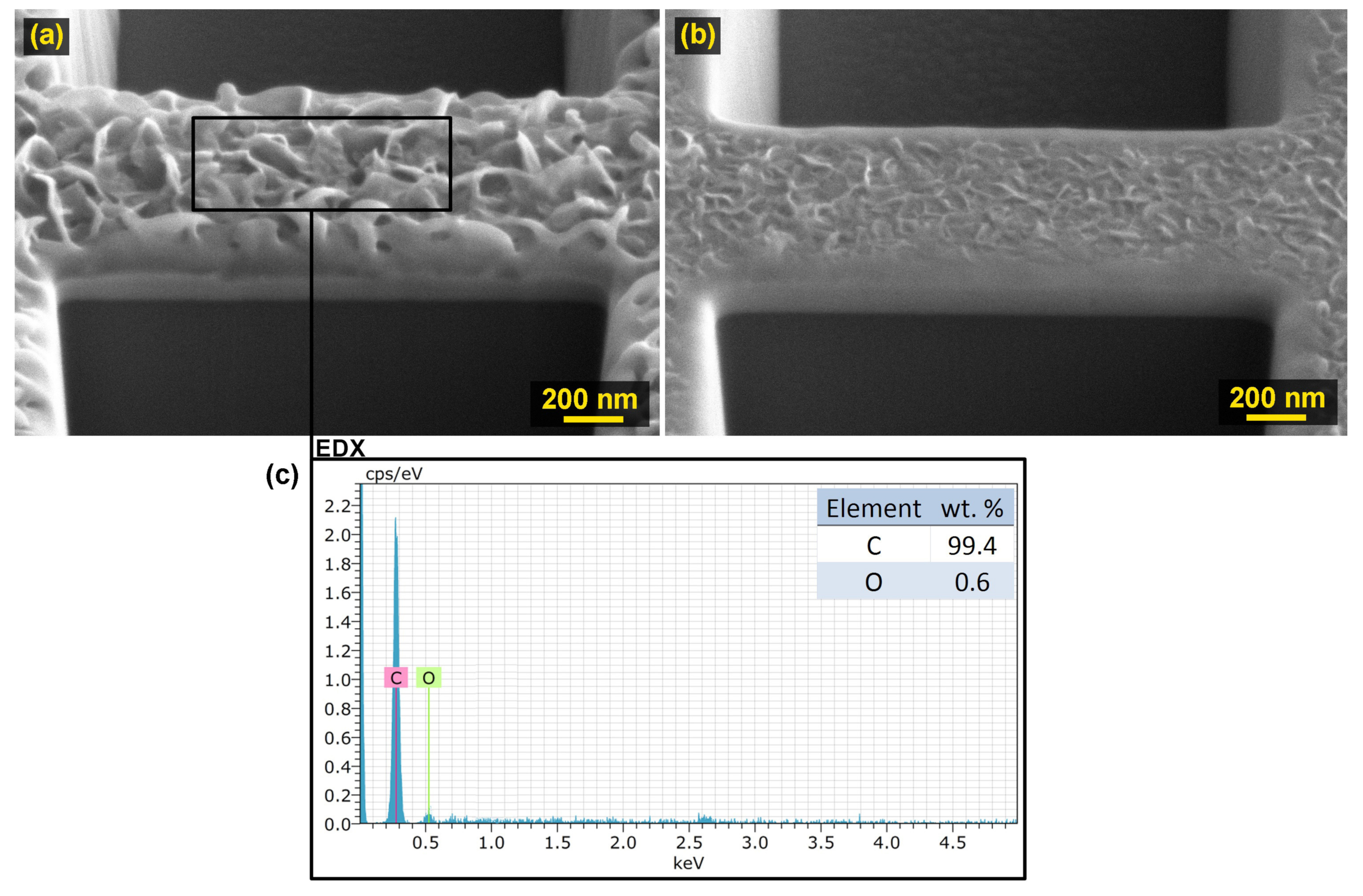
To show a comparison of the height and total occurrence of graphene, Sample 50 (Flow 100 sccm, Plasma power 300 W and Annealing in H2 30 sccm) was selected with the lowest vertical graphene thickness, which was only 146 nm, and Sample 1, on which vertical graphene has not grown almost at all. These two cross-sections of the sample were shown in Figure 1a,b, and to determine the chemical composition, an EDX analysis was performed showing the presence of carbon, which was 99.4 wt.%. Oxygen (0.6 wt.%) was also present in a small part, which indicates a slight oxidation of the surface.
The height of the vertical graphene was measured using an electron microscope equipped with a FIB, in which a double-sided ditch with a depth of 4 μm, a width of 10 μm and a gap of 2 μm was deepened. This was used to display the interface of the base material AlCu4Mg and the overposed vertical graphene. The graphene height function, which was part of the electron microscope software, always measured the height of the graphene. The measured thickness values were entered in Table 1, from which it is clear that the highest thickness of 310 nm was reached in Sample 54. In contrast, the lowest thickness of vertical graphene was measured in Sample 50 and only 146 nm. In this case, these were samples for which all parameters were set identically to the parameter Annealing in H2, which was set to a maximum value of 150 sccm for the sample with the highest thickness and to a minimum value of 30 sccm for the sample with the lowest thickness. The maximum thickness here is significantly lower than in the case of the growth of vertical graphene on a silver substrate, where a thickness of up to 480 nm was reached [22]. The growth of vertical graphene on this aluminum alloy has not yet been studied, so a comparison is not possible.
The topography of the vertical graphene was analyzed by AFM, and the measurement was performed with a special tip with a radius of 10 nm in tapping mode. Sample 50 (Flow 100 sccm, Plasma power 300 W and Annealing in H2 30 sccm) was selected for this topography analysis due to the lowest thickness of individual vertical graphene, because despite the use of a tip with a radius of 10 nm, the results of displaying higher graphene thicknesses were not satisfying. The shape of the tip also affected the shape of the vertices of the vertical graphene, as can be seen in the images shown in Figure 2. The reason is the rounding of the tip, which arose during its production, which consisted of milling with an ion beam in an electron microscope. The maximum measured height according to the AFM images thus does not correspond to the measured value given in Table 1, because when measured in an electron microscope, there was no distortion caused by the manufacture of the measuring device - in this case the tip. Therefore, the information on the AFM image can only be considered indicative and not accurate. The same measurement and imaging error was also noted for images in similar studies that displayed vertical graphene using the AFM technique, such as Qi [23] or Shokrieh [24].
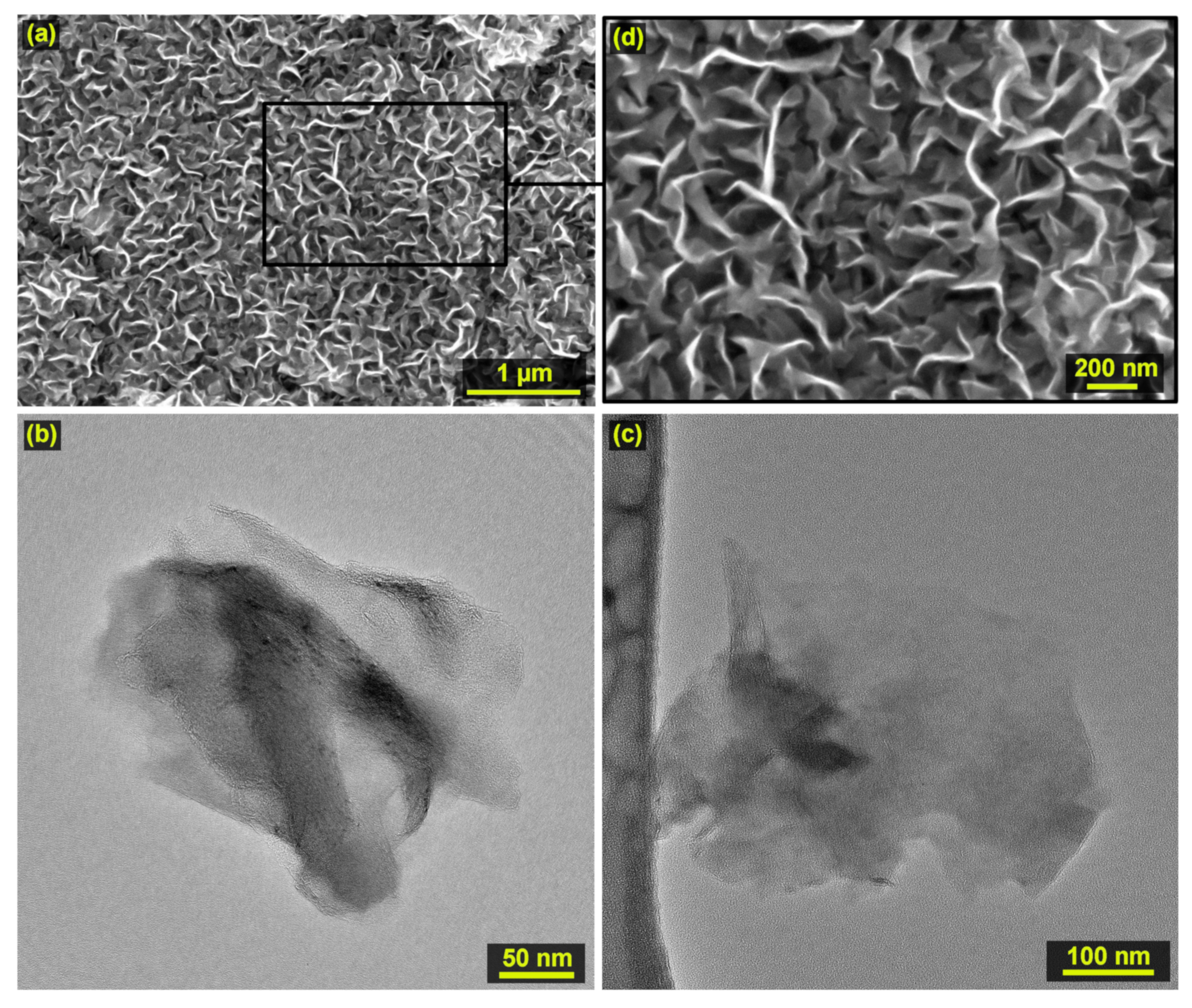
Due to the distortion that occurred when imaging vertical graphene using AFM, an electron microscope was used for more accurate imaging. Its images are much more accurate and show its true appearance. An image of the same sample that was used for AFM imaging was also used here, i.e., Sample 50 (Flow 100 sccm, Plasma power 300 W, and Annealing in H2 30 sccm) with the lowest vertical graphene thickness, which was only 146 nm. From the image shown in Figure 3, the vertical shape of the individual grapheme is clearly visible. Vertical graphene forms a dense network that has a large active area compared to the horizontal type of graphene. The same imaging of superimposed graphene was obtained in studies Zhang [25], Ma [26], Sha [27], or Xie [28].
For an even more detailed examination, observations were made in a transmission electron microscope. For this reason, a 1:1 solution of ethanol and water was prepared, and a thin layer of vertical graphene was scraped from the base material by means of a scalpel into the solution thus prepared. 1μL of the solution was pipetted onto the membrane and dried. Due to the same value of the surface energy of the solution with the magnitude of the Van der Waals energy between the individual graphene layers, there is no aggregation of materials in the solution. Figure 3b shows vertical graphene observed in TEM, showing the individual carbon atoms arranged in the crystalline planes. A similar display of vertical graphene in TEM was achieved in studies Yao [29] Xia [30] and Zhao [19].
3.2. Raman Spectroscopy
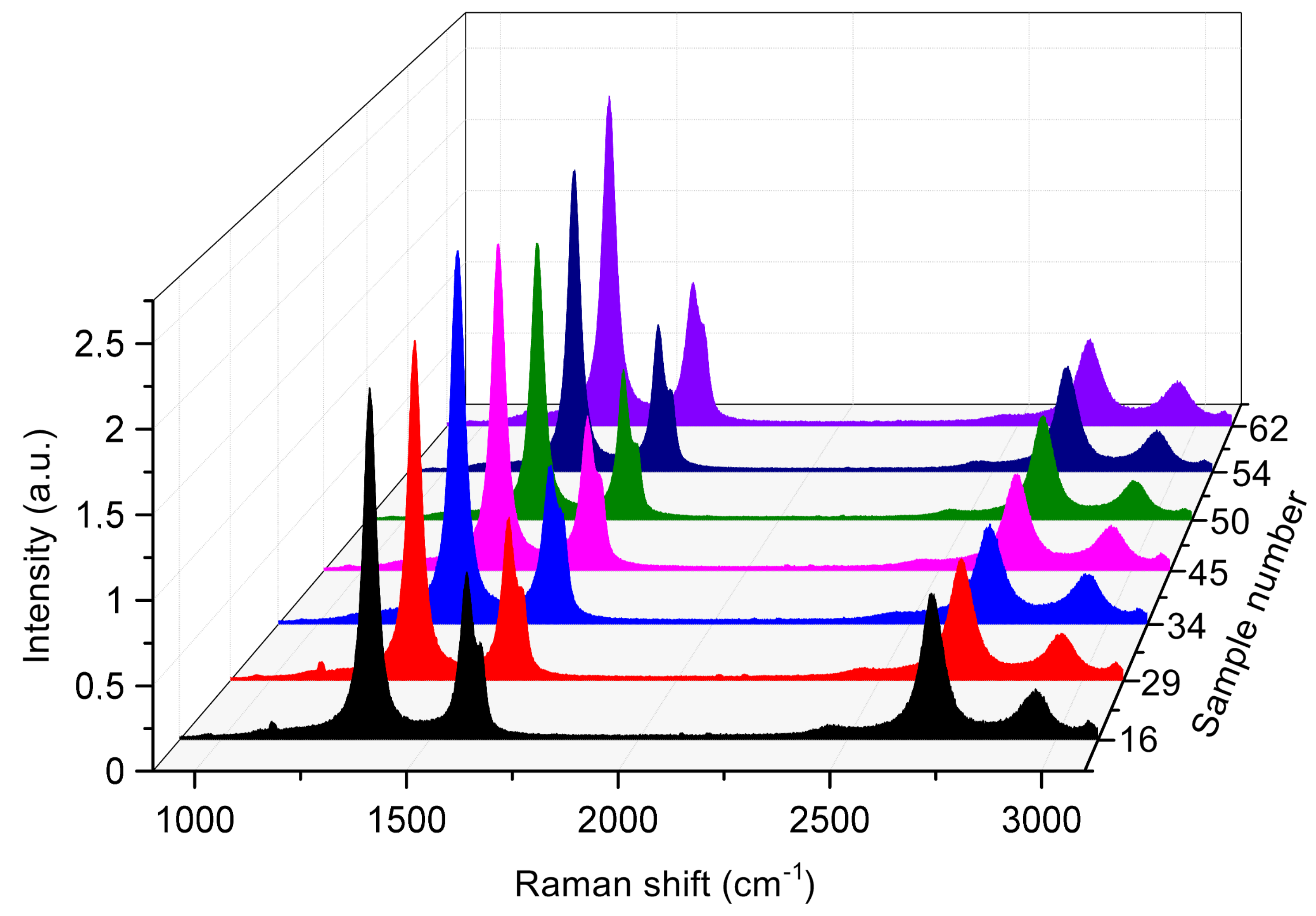
Raman spectroscopy showed graphene deposition in all 7 cases of its growth according to Table 1. The characteristic Raman peaks for graphitic materials (1580 cm−1) and 2D (2700 cm−1) were studied here. The normalized Raman spectrum according to the G peak for the samples on which growth occurred, namely Sample 16, 29, 34, 45, 50, 54, and 62, are shown in Figure 4.
In addition to the standard graphene peaks (G, 2D), several additional peaks were discovered in the Raman spectrum, which were D, D + D′ and D + D‴ as well as D′, D″. These peaks, except for D′, which is caused by the final size of the graphene crystal, are only a combined manifestation of defects in the graphene crystal lattice. The large number of defects detected by the Raman spectrum is due to the imperfect crystalline structure of the edges of the vertical graphene, the nanographitic base layer, and the ionic damage that occurred during the deposition itself. The ratios between the 2D/G and D/G peaks are given in Table 2. The value of the 2D/G peak ratio characterizes the number of its layers [27] and the D/G ratio describes the degree of graphitization (the form of the structure approaching graphite) [26].
By comparing the data from Table 1, Table 2 for Samples 50 and 54, it is clear that the annealing parameter in H2 affects the number of defects in the graphene layer, i.e., the D/G ratio. The more hydrogen, the higherthe D/G ratio. When setting the lower values of the Power parameter, for Samples 16 and 29, this effect is minimal. An exception, however, are Samples 34 and 62, where a significant effect of the annealing parameter in H2 was found. The probable reason is the low amount of gas in the deposition atmosphere, where the Flow parameter is only at 30 sccm and not 100 sccm, as is the case with Samples 16 and 29. By comparing Samples 16 and 29 in terms of 2D/G ratio, it is clear that a lower value of the annealing parameter in H2 leads to a higher value of the ratio. Unfortunately, at higher values of the Performance parameter, Samples 50 and 54 do not show the same trend as for the above-mentioned samples. From the measured values of the 2D/G ratios it follows that in Samples 16, 29, 34, 45, 50, 54, and 62 there was deposition according to the definition and thus the growth of several layers of graphene. A 2D/G ratio value of 0.9 to 0.6 corresponds to 3 to 5 layers of planar graphene. A comparison of the data for the different values of the power parameter shows that a higher value of the plasma power reduces the 2D/G ratio, which is related to the higher energy of the system during deposition. This finding was also made in Sandoz-Rosado [31].
3.3. Statistical Evaluation of Graphene Growth
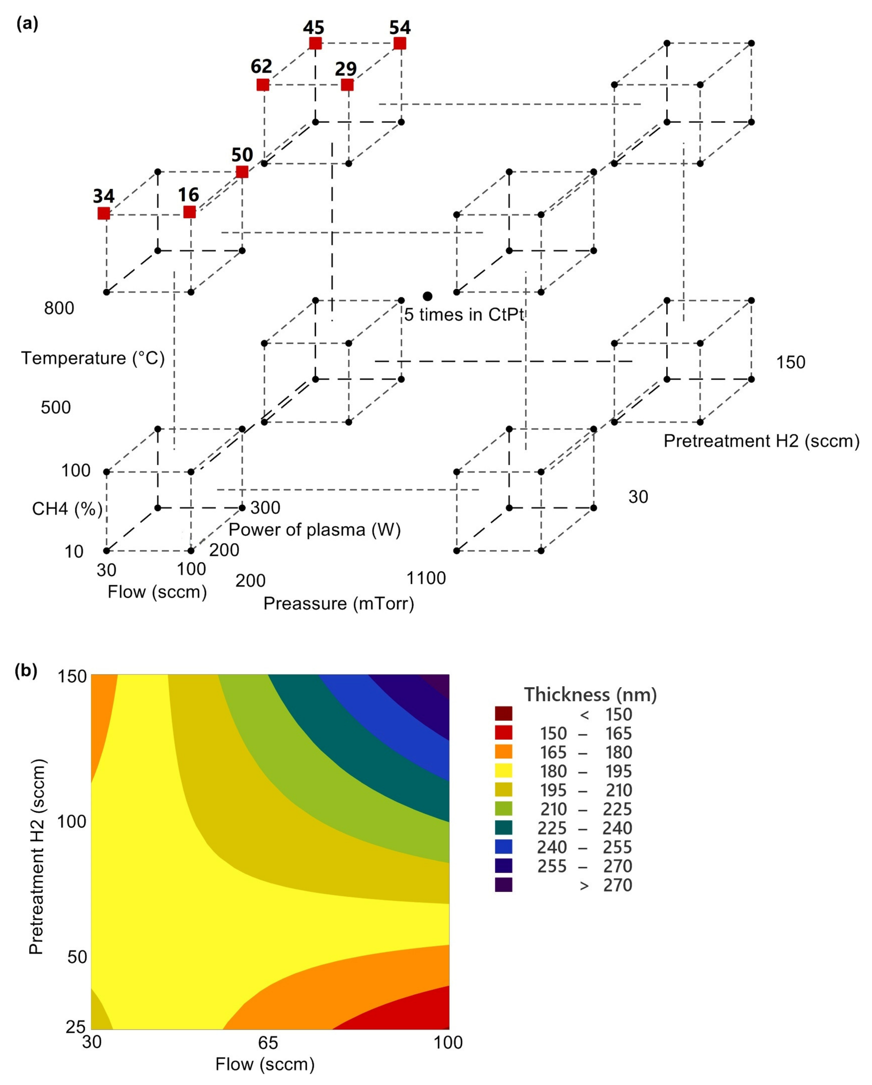
The planned binary logistic regression does not need to be done because the factors Temperature, Pressure, and CH4 divided the experimental inlet space into an area where the vertical graphene grows and does not increase except for one point. The projection of the entire experimental five-dimensional space, including the points where the graphene grows marked with a red square and a sample number, is shown in Figure 5a.
Classical linear regression can now be used to model the thickness of vertical graphene depending on the remaining three parameters Flow (sccm), Power of plasma (W), and Pretreatment H2 (sccm). A regression model was created for all predictors and their second order interactions, from which individual statistically insignificant terms were removed by the Backward Elimination method while maintaining the hierarchy of the model. The resulting regression model describes about 90% of the variability of the monitored graphene thicknesses (R2 = 90.49%) and is shown in the following Equation (1):
Thickness (nm) = 242.3 − 1.259 Flow (sccm) − 0.776 Pretreatment H2 (sccm) +
0.01863 Flow (sccm) × Pretreatment H2 (sccm)
0.01863 Flow (sccm) × Pretreatment H2 (sccm)
Only the Flow (sccm) × H2 Pretreatment (sccm) interaction is statistically significant (p-value < 0.05). The factors themselves are statistically insignificant and are left in the equation to maintain the model hierarchy. The P-values of the individual regression terms, including their contribution to the explanation of the variability of the monitored vertical graphene thicknesses, are given in Table 3. A graphical representation of the dependence of the thickness of the vertical graphene on the monitored parameters is shown in Figure 5b, where a significant interaction, a saddle-shaped curvature of the response surface, occurred.
For this model, due to the number of measurements, it is not possible to do a statistical test of the adequacy of the model (Lack of Fit test). If it were not insisted on the requirement of the model hierarchy, model (2) with R2 = 75.07% would be obtained, where the Lack of Fit test can be performed. p-valueLack of Fit = 0.236 > 0.05 and model (2) is therefore adequate. Thanks to the statistical properties of the hierarchical model (1), we would like to adhere to it, also because it is in step with the procedure described in Montgomary [32].
Thickness (nm) = 142.2 + 0.00879 Flow (sccm) × Pretreatment H2 (sccm)
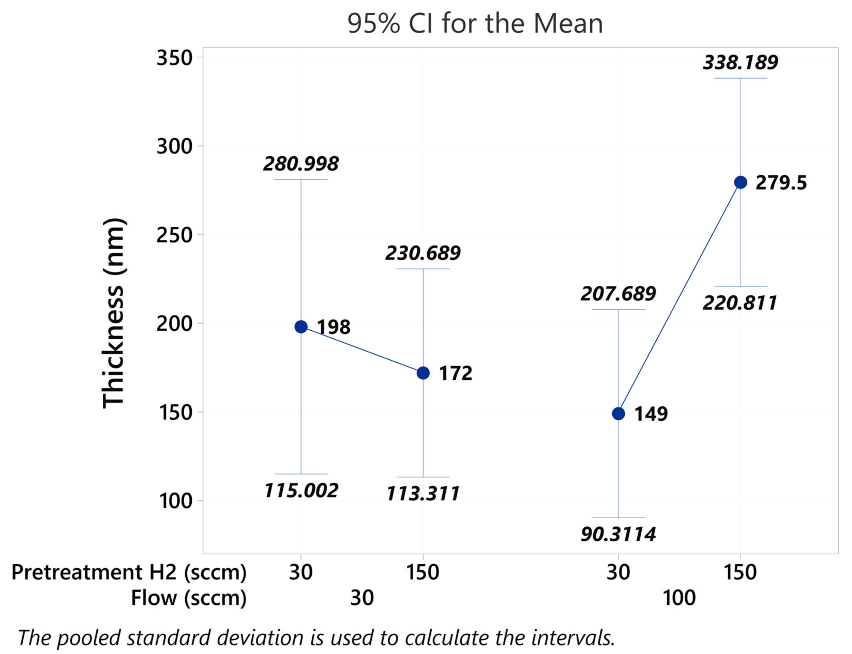
The individual factors have an insignificant effect on the thickness of the vertical graphene, so their interaction was plotted, which is significant, including interval estimates of mean values with 95% of confidence (Figure 6). The interaction is the interaction of factors on the response and is graphically expressed as the non-uniformity of the lines connecting the mean values. Pooled standard deviation was used to calculate the interval estimates because the homogeneity of variance is a prerequisite for the regression models listed above. It should be noted here that it is the effect of this interaction on the thickness of the vertical graphene when the temperature is fixed at 800 °C, the chamber pressure is 200 mTorr, simultaneously with the methane content at 100%. In other cases, there was no increase in graphene [33,34].
4. Conclusions
The analysis of the growth of vertical graphene on the aluminum alloy AlCu4Mg using PECVD technology was performed using a design of experiment of 69 rounds, followed by an evaluation of its growth and further analysis, which reached the following conclusions:
- After performing the design of the experiment, it was found that the growth of vertical graphene occurred in only 7 cases, always when setting the parameter Temperature to 800 °C, Pressure to 200 mTorr and CH4 to 100%, while the other three parameters Flow, Plasma power, and Annealing in H2 were different,
- The highest thickness of 310 nm was reached for Sample 54 (Flow 100 sccm, Plasma power 300 W, and Annealing in H2 150 sccm) and, conversely, the lowest thickness for Sample 50 (Flow 100 sccm, Plasma power 300 W and Annealing in H2 30 sccm) and only 146 nm,
- Imaging of deposited vertical graphene was performed using AFM, SEM, and TEM,
- Raman spectroscopy showed the deposition of vertical graphene in all 7 cases of its growth and in the Raman spectrum, in addition to standard graphene peaks (G, 2D), several additional ones were discovered, which were D, D + D′, and D + D″ and also D′, D″,
- A comparison of the data for the different values of the Power parameter shows that a higher value of the plasma power reduces the 2D/G ratio, which is related to the higher energy of the system during deposition,
- A regression model was created describing about 90% of the variability of the monitored graphene thicknesses, while only the Flow (sccm) interaction is statistically significant × Pretreatment H2 (sccm).
From the above conclusions, it can be clearly stated that the objectives of this study were fully met, because there was an increase in vertical graphene on the base material, which was an aluminum alloy AlCu4Mg. This clearly defines the high potential for further improving the performance of a given aluminum alloy in the packaging industry.
Author Contributions
A.P.: Conceptualization, Methodology, Data curation, Writing—Original draft preparation, Writing—Reviewing and Editing, Supervision. J.S. (Josef Sedlak): Validation, Visualization, Formal analysis. J.S. (Jan Sedlacek): Methodology, Data curation. L.B.: Funding acquisition. K.M.: Methodology, Data curation. All authors have read and agreed to the published version of the manuscript.
Funding
This work was supported by the grant “Application of the New Surface Treatment Technologies in Metal Packaging Industry“, PID: FV40313, Ministry of Industry and Trade, The Czech Republic. CzechNanoLab project LM2018110 funded by MEYS CR is gratefully acknowledged for the financial support of the measurements/sample fabrication at CEITEC Nano Research Infrastructure.
Institutional Review Board Statement
Not applicable.
Informed Consent Statement
Not applicable.
Data Availability Statement
The data presented in this study are available on request from the corresponding author. The data are not publicly available due to company secret.
Conflicts of Interest
Authors A. Polzer, J. Sedlak, J. Sedlacek, L. Benes, K. Mouralova declare that they have no conflict of interest.
References
- Johnson, L.; Meany, J.E. Graphene: The Superstrong, Superthin, and Superversatile Material That Will Revolutionize the World; Prometheus Books: Buffalo, NY, USA, 2018; ISBN 9781633883260. [Google Scholar]
- Chen, J.H.; Jang, C.; Xiao, S.; Ishigami, M.; Fuhrer, M.S. Intrinsic and extrinsic performance limits of graphene devices on SiO2. Nat. Nanotechnol. 2008, 3, 206–209. [Google Scholar] [CrossRef]
- Lee, C.; Wei, X.; Kysar, J.W.; Hone, J. Measurement of the elastic properties and intrinsic strength of monolayer graphene. Science 2008, 321, 385–388. [Google Scholar] [CrossRef] [PubMed]
- Van Lier, G.; Van Alsenoy, C.; Van Doren, V.; Geerlings, P. Ab initio study of the elastic properties of single-walled carbon nanotubes and graphene. Chem. Phys. Lett. 2000, 326, 181–185. [Google Scholar] [CrossRef]
- Chen, J.; Bo, Z.; Lu, G. Vertically-Oriented Graphene; Springer International Publishing: Cham, Switzerland, 2015; ISBN 978-3-319-15302-5. [Google Scholar]
- Tiwari, A. (Ed.) Graphene Bioelectronics; Elsevier: Amsterdam, The Netherlands, 2017; ISBN 978-0-12-813349-1. [Google Scholar]
- Yerlanuly, Y.; Christy, D.; Van Nong, N.; Kondo, H.; Alpysbayeva, B.; Nemkayeva, R.; Kadyr, M.; Ramazanov, T.; Gabdullin, M.; Batryshev, D.; et al. Synthesis of carbon nanowalls on the surface of nanoporous alumina membranes by RI-PECVD method. Appl. Surf. Sci. 2020, 523, 146533. [Google Scholar] [CrossRef]
- Davami, K.; Jiang, Y.; Cortes, J.; Lin, C.; Shaygan, M.; Turner, K.T.; Bargatin, I. Tuning the mechanical properties of vertical graphene sheets through atomic layer deposition. Nanotechnology 2016, 27, 155701. [Google Scholar] [CrossRef]
- Hussain, S.; Kovacevic, E.; Berndt, J.; Santhosh, N.M.; Pattyn, C.; Dias, A.; Cvelbar, U. Low-temperature low-power PECVD synthesis of vertically aligned graphene. Nanotechnology 2020, 31, 395604. [Google Scholar] [CrossRef] [PubMed]
- Wang, K.; Wang, C.; Yang, H.; Wang, X.; Cao, F.; Wu, Q.; Peng, H. Vertical graphene nanosheetsmodified Al current collectors for high-performance sodium-ion batteries. Nano Res. 2020, 13, 1948–1954. [Google Scholar] [CrossRef]
- Premathilake, D.; Outlaw, R.A.; Parler, S.G.; Butler, S.M.; Miller, J.R. Electric double layer capacitors for ac filtering made from vertically oriented graphene nanosheets on aluminum. Carbon 2017, 111, 231–237. [Google Scholar] [CrossRef]
- Li, W.; Islam, N.; Ren, G.; Li, S.; Fan, Z. AC-filtering supercapacitors based on edge oriented vertical graphene and cross-linked carbon nanofiber. Materials 2019, 12, 604. [Google Scholar] [CrossRef] [Green Version]
- Kumar, M.; Khanna, S.; Gupta, N.; Gupta, R.; Sharma, S.C. Numerical simulation and parametric study of carbon deposition during graphene growth in PECVD system. IEEE Trans. Nanotechnol. 2019, 18, 401–411. [Google Scholar] [CrossRef]
- Hu, Z.; Li, Z.; Xia, Z.; Jiang, T.; Wang, G.; Sun, J.; Sun, P.; Yan, C.; Zhang, L. PECVD-derived graphene nanowall/lithium composite anodes towards highly stable lithium metal batteries. Energy Storage Mater. 2019, 22, 29–39. [Google Scholar] [CrossRef]
- Yeh, N.C.; Hsu, C.C.; Bagley, J.; Tseng, W.S. Single-step growth of graphene and graphene-based nanostructures by plasma-enhanced chemical vapor deposition. Nanotechnology 2019, 30, 162001. [Google Scholar] [CrossRef] [PubMed] [Green Version]
- Schmidt, S.; Greczynski, G.; Goyenola, C.; Gueorguiev, G.K.; Czigány, Z.; Jensen, J.; Ivanov, I.G.; Hultman, L. CFx thin solid films deposited by high power impulse magnetron sputtering: Synthesis and characterization. Surf. Coat. Technol. 2011, 206, 646–653. [Google Scholar] [CrossRef] [Green Version]
- Gueorguiev, G.K.; Goyenola, C.; Schmidt, S.; Hultman, L. CFx: A first-principles study of structural patterns arising during synthetic growth. Chem. Phys. Lett. 2011, 516, 62–67. [Google Scholar] [CrossRef] [Green Version]
- Högberg, H.; Lai, C.C.; Broitman, E.; Ivanov, I.G.; Goyenola, C.; Näslund, L.Å.; Schmidt, S.; Hultman, L.; Rosen, J.; Gueorguiev, G.K. Reactive sputtering of CSx thin solid films using CS2 as precursor. Vacuum 2020, 182, 109775. [Google Scholar] [CrossRef]
- Zhao, J.; Shaygan, M.; Eckert, J.; Meyyappan, M.; Rümmeli, M.H. A growth mechanism for free-standing vertical graphene. Nano Lett. 2014, 14, 3064–3071. [Google Scholar] [CrossRef] [PubMed]
- Chugh, S.; Mehta, R.; Lu, N.; Dios, F.D.; Kim, M.J.; Chen, Z. Comparison of graphene growth on arbitrary non-catalytic substrates using low-temperature PECVD. Carbon 2015, 93, 393–399. [Google Scholar] [CrossRef]
- Bo, Z.; Yang, Y.; Chen, J.; Yu, K.; Yan, J.; Cen, K. Plasma-enhanced chemical vapor deposition synthesis of vertically oriented graphene nanosheets. Nanoscale 2013, 5, 5180–5204. [Google Scholar] [CrossRef] [PubMed] [Green Version]
- Mouralova, K.; Zahradnicek, R.; Bednar, J. Study of vertical graphene growth on silver substrate based on design of experiment. Diam. Relat. Mater. 2019, 97, 107439. [Google Scholar] [CrossRef]
- Qi, Y.; Deng, B.; Guo, X.; Chen, S.; Gao, J.; Li, T.; Dou, Z.; Ci, H.; Sun, J.; Chen, Z.; et al. Switching vertical to horizontal graphene growth using faraday cage-assisted PECVD approach for high-performance transparent heating device. Adv. Mater. 2018, 30, 1704839. [Google Scholar] [CrossRef] [PubMed]
- Shokrieh, M.M.; Hosseinkhani, M.R.; Naimi-Jamal, M.R.; Tourani, H.J.P.T. Nanoindentation and nanoscratch investigations on graphene-based nanocomposites. Polym. Test. 2013, 32, 45–51. [Google Scholar] [CrossRef]
- Zhang, L.X.; Sun, Z.; Qi, J.L.; Shi, J.M.; Hao, T.D.; Feng, J.C. Understanding the growth mechanism of vertically aligned graphene and control of its wettability. Carbon 2016, 103, 339–345. [Google Scholar] [CrossRef]
- Ma, Y.; Jang, H.; Kim, S.J.; Pang, C.; Chae, H. Copper-assisted direct growth of vertical graphene nanosheets on glass substrates by low-temperature plasma-enhanced chemical vapour deposition process. Nanoscale Res. Lett. 2015, 10, 1–8. [Google Scholar] [CrossRef] [Green Version]
- Sha, Z.; Han, Z.; Wu, S.; Zhang, F.; Islam, M.S.; Brown, S.A.; Wang, C.H. Low-temperature plasma assisted growth of vertical graphene for enhancing carbon fibre/epoxy interfacial strength. Compos. Sci. Technol. 2019, 184, 107867. [Google Scholar] [CrossRef]
- Xie, D.; Xia, X.; Zhong, Y.; Wang, Y.; Wang, D.; Wang, X.; Tu, J. Exploring advanced sandwiched arrays by vertical graphene and N-doped carbon for enhanced sodium storage. Adv. Energy Mater. 2017, 7, 1601804. [Google Scholar] [CrossRef]
- Yao, Z.; Xia, X.; Zhong, Y.; Wang, Y.; Zhang, B.; Xie, D.; Wang, X.; Tu, J.; Huang, Y. Hybrid vertical graphene/lithium titanate–CNTs arrays for lithium-ion storage with extraordinary performance. J. Mater. Chem. A 2017, 5, 8916–8921. [Google Scholar] [CrossRef]
- Xia, X.; Deng, S.; Xie, D.; Wang, Y.; Feng, S.; Wu, J.; Tu, J. Boosting sodium ion storage by anchoring MoO2 on vertical graphene arrays. J. Mater. Chem. A 2018, 6, 15546–15552. [Google Scholar] [CrossRef]
- Sandoz-Rosado, E.; Page, W.; O’Brien, D.; Przepioski, J.; Mo, D.; Wang, B.; Ngo-Duc, T.T.; Gacusan, J.; Winter, M.W.; Meyyappan, M.; et al. Vertical graphene by plasma-enhanced chemical vapor deposition: Correlation of plasma conditions and growth characteristics. J. Mater. Res. 2014, 29, 417–425. [Google Scholar] [CrossRef]
- Montgomery, D.C. Design and Analysis of Experiments; John Wiley&Sons Inc.: Hoboken, NJ, USA, 2017; ISBN 9781119113478. [Google Scholar]
- Li, D.; Wang, H.; Wang, X. Effect of microstructure on the modulus of PAN-based carbon fibers during high temperature treatment and hot stretching graphitization. J. Mater. Sci. 2007, 42, 4642–4649. [Google Scholar] [CrossRef]
- Şimşek, B. TOPSIS based Taguchi design optimization for CVD growth of graphene using different carbon sources: Graphene thickness, defectiveness and homogeneity. Chin. J. Chem. Eng. 2019, 27, 685–694. [Google Scholar] [CrossRef]
Figure 1.
(a) section of Sample 50 and EDX analysis on the marked area (SEM/SE), (b) section of Sample 1, where the vertical graphene did not grow at all (SEM/SE), (c) EDX analysis.
Figure 1.
(a) section of Sample 50 and EDX analysis on the marked area (SEM/SE), (b) section of Sample 1, where the vertical graphene did not grow at all (SEM/SE), (c) EDX analysis.

Figure 2.
Topography of vertical graphene displayed in 2D and 3D, including a detailed view of the marked area, (a) 2D picture, (b) 3D picture, (c) 2D picture of detail A, (d) 3D picture of detail A.
Figure 2.
Topography of vertical graphene displayed in 2D and 3D, including a detailed view of the marked area, (a) 2D picture, (b) 3D picture, (c) 2D picture of detail A, (d) 3D picture of detail A.

Figure 3.
(a) an image of vertical graphene from Sample 50 (SEM/SE), (b,c) vertical graphene observed in TEM, (d) detail of picture (a).
Figure 3.
(a) an image of vertical graphene from Sample 50 (SEM/SE), (b,c) vertical graphene observed in TEM, (d) detail of picture (a).

Figure 4.
Raman spectra of vertical graphene for individual samples.

Figure 5.
(a) Occurrence of vertical graphene with respect to the setting of input parameters, (b) Contour Plot of Thicknesses Pretreatment H2 and Flow.
Figure 5.
(a) Occurrence of vertical graphene with respect to the setting of input parameters, (b) Contour Plot of Thicknesses Pretreatment H2 and Flow.

Figure 6.
Interval Plot of Thickness (nm) with Interaction Flow × Pretreatment H2.


Table 1.
Process Parameters of PECVD Deposition of Vertical Graphene at which it Grew.
| Sample Number | Flow (sccm) | Plasma Power (W) | AnnealinginH2 (sccm) | Temperature (°C) | CH4 (%) | Pressure (mTorr) | Thickness (nm) |
|---|---|---|---|---|---|---|---|
| 16 | 100 | 200 | 30 | 800 | 100 | 200 | 152 |
| 29 | 100 | 200 | 150 | 800 | 100 | 200 | 249 |
| 34 | 30 | 200 | 30 | 800 | 100 | 200 | 198 |
| 45 | 30 | 300 | 150 | 800 | 100 | 200 | 163 |
| 50 | 100 | 300 | 30 | 800 | 100 | 200 | 146 |
| 54 | 100 | 300 | 150 | 800 | 100 | 200 | 310 |
| 62 | 30 | 200 | 150 | 800 | 100 | 200 | 181 |
Table 2.
Ratios of Individual Raman Peaks Studied in Vertical Graphene.
| Sample Number | 2D/G | D/G |
|---|---|---|
| 16 | 0.874722 | 2.092911 |
| 29 | 0.746302 | 2.076457 |
| 34 | 0.631852 | 2.342962 |
| 45 | 0.627815 | 2.103282 |
| 50 | 0.691447 | 1.832055 |
| 54 | 0.718845 | 2.038826 |
| 62 | 0.609512 | 2.29333 |
Table 3.
Analysis of Regression Model Variance.
| Source | p-Value | Contribution of Model Variability |
|---|---|---|
| Constant | 0.015 | - |
| Flow (sccm) | 0.118 | 9.01% |
| Pretreatment H2 (sccm) | 0.142 | 35.81% |
| Flow (sccm) ×Pretreatment H2 (sccm) | 0.032 | 45.66% |
| Error | 9.51% | |
| Total | 100.00% |
Publisher’s Note: MDPI stays neutral with regard to jurisdictional claims in published maps and institutional affiliations. |
© 2021 by the authors. Licensee MDPI, Basel, Switzerland. This article is an open access article distributed under the terms and conditions of the Creative Commons Attribution (CC BY) license (https://creativecommons.org/licenses/by/4.0/).
Share and Cite
MDPI and ACS Style
Polzer, A.; Sedlak, J.; Sedlacek, J.; Benes, L.; Mouralova, K. Vertical Graphene Growth on AlCu4Mg Alloy by PECVD Technique. Coatings 2021, 11, 1108. https://doi.org/10.3390/coatings11091108
AMA Style
Polzer A, Sedlak J, Sedlacek J, Benes L, Mouralova K. Vertical Graphene Growth on AlCu4Mg Alloy by PECVD Technique. Coatings. 2021; 11(9):1108. https://doi.org/10.3390/coatings11091108
Chicago/Turabian StylePolzer, Ales, Josef Sedlak, Jan Sedlacek, Libor Benes, and Katerina Mouralova. 2021. "Vertical Graphene Growth on AlCu4Mg Alloy by PECVD Technique" Coatings 11, no. 9: 1108. https://doi.org/10.3390/coatings11091108
Note that from the first issue of 2016, this journal uses article numbers instead of page numbers. See further details here.