Article

Influence of Substrate Materials on Nucleation and Properties of Iridium Thin Films Grown by ALD

1
Institute of Applied Physics IAP, Friedrich Schiller University Jena, Albert-Einstein-Str. 15, D-07745 Jena, Germany
2
Fraunhofer Institute for Applied Optics and Precision Engineering IOF, Center of Excellence in Photonics, Albert-Einstein-Str. 7, D-07745 Jena, Germany
3
Institute of Solid State Physics IFK, Friedrich Schiller University Jena, Helmholtzweg 5, D-07743 Jena, Germany
*
Author to whom correspondence should be addressed.
Coatings 2021, 11(2), 173; https://doi.org/10.3390/coatings11020173
Submission received: 18 December 2020 / Revised: 18 January 2021 / Accepted: 29 January 2021 / Published: 2 February 2021
(This article belongs to the Special Issue Recent Advances in Optical Thin Films Coatings)

Abstract

:
Ultra-thin metallic films are widely applied in optics and microelectronics. However, their properties differ significantly from the bulk material and depend on the substrate material. The nucleation, film growth, and layer properties of atomic layer deposited (ALD) iridium thin films are evaluated on silicon wafers, BK7, fused silica, SiO2, TiO2, Ta2O5, Al2O3, HfO2, Ru, Cr, Mo, and graphite to understand the influence of various substrate materials. This comprehensive study was carried out using scanning electron and atomic force microscopy, X-ray reflectivity and diffraction, four-point probe resistivity and contact angle measurements, tape tests, and Auger electron spectroscopy. Within few ALD cycles, iridium islands occur on all substrates. Nevertheless, their size, shape, and distribution depend on the substrate. Ultra-thin (almost) closed Ir layers grow on a Ta2O5 seed layer after 100 cycles corresponding to about 5 nm film thickness. In contrast, the growth on Al2O3 and HfO2 is strongly inhibited. The iridium growth on silicon wafers is overall linear. On BK7, fused silica, SiO2, TiO2, Ta2O5, Ru, Cr, and graphite, three different growth regimes are distinguishable. The surface free energy of the substrates correlates with their iridium nucleation delay. Our work, therefore, demonstrates that substrates can significantly tailor the properties of ultra-thin films.

Graphical Abstract

1. Introduction

The noble metal iridium (Ir) is applied in various areas, such as for optics [1], sensors [2,3], and catalysts [4,5], as electrodes [6], protective layers [7,8], or hydrogen separation membranes [9]. Among others, iridium is essential for different high-performance optical elements, such as metal wire grid polarizers [10], Fresnel zone plates [11], and curved grazing incidence mirrors [12]. For the conformal coating of these structurally complex elements, atomic layer deposition (ALD) is the method of choice. Conventional deposition techniques, like sputtering or evaporation, reach their technological limitations for such micro-structured or strongly curved substrates. With optical elements becoming more and more complex, the importance of conformal ALD coatings increases. Additionally, ultra-thin metallic films with a thickness of few nanometers are widely desired for optical and electrical applications but challenging to obtain.
Atomic layer deposition is a chemical deposition technique based on sequential and self-limiting surface reactions. Each ALD cycle consists of four sequential steps: precursor pulse, precursor purge, co-reactant pulse, and co-reactant purge. The two gaseous precursors react exclusively with the available functional groups on the substrate surface. Purging steps with inert gas prevent undesired chemical reactions between the precursors or their by-products. This process allows the deposition of conformal and uniform thin films with precise thickness control. [13,14] Since the ALD layer formation is based on chemical surface reactions, other growth mechanisms can occur. Chemical conditions on the substrate surface combined with the precursors determine whether and how a thin film forms. This principle fundamentally differs from conventional deposition techniques, like sputtering or evaporation, in which the material source determines the deposited amount of material.
Over the last 20 years, numerous new ALD precursors and processes for the noble metals Ru [15], Rh [16], Pd [17], Ag [18], Os [19], Pt [20], Au [21], and Ir were developed due to their outstanding physical properties and wide range of applications [22]. For iridium, five precursors Ir(acac)3 [23], IrF6 [24], Ir(CpEt)(cod) [25], Ir(CpMe)(chd) [26], and Ir(CpEt)(chd) [27] are applied in ALD processes. Many studies report on optimizing process parameters for different co-reactants [28,29] or special applications [30,31,32,33]. However, the nucleation and growth of Ir ALD thin films on various substrates have not been investigated yet in detail. The material properties and, consequently, the performance of devices depend strongly on the substrate material.
This article aims to better understand the nucleation and layer formation of thin metallic Ir films in thermal ALD processes using the Ir(acac)3 precursor. In particular, the influence of different substrate materials on layer formation and layer properties is investigated. Here, the optimized process parameters for the film growth of Ir (on silicon wafers) were kept constant. The comprehensive results provide new insights into the growth behavior of metallic ALD coatings and their interaction with the substrate materials.
The results of this article are divided into three parts. In the first part, the nucleation of iridium, meaning the initial layer formation, is investigated on different substrate materials. Therefore, primarily scanning electron microscopy (SEM) images were evaluated both qualitatively and quantitatively. The second part is dedicated to the Ir layer growth from nucleation via the formation of a closed layer towards film thickness growth. Mainly X-ray reflectivity (XRR) and four-point probe resistivity measurement, as well as water contact angle measurements, were applied. The third part focuses on the properties of thick Ir coatings depending on the substrate materials. These properties were studied by atomic force microscopy (AFM), X-ray diffraction (XRD), four-point probe resistivity measurement, tape tests, and Auger electron spectroscopy (AES).

2. Materials and Methods

2.1. Substrate Materials

As bare substrates, silicon (Si) wafers with a native SiO2 layer, borosilicate crown glass (BK7), and fused silica were used. The single-crystalline Si wafers were p-doped, (100)-oriented, and double-side polished with a surface roughness (1 × 1 µm2) of about 0.15 nm root-mean-square (rms). The amorphous BK7 and fused silica substrates had a surface roughness of 1.9 nm rms and 0.26 nm rms, respectively, and a diameter of 25 mm. These substrates were cleaned with a multi-stage, ultrasonic-assisted bath cleaning system (Elma Schmidbauer, Singen, Germany), which consisted of alkaline, tenside, and water baths followed by a final bath of deionized ultrapure water.
In addition, seed layers of SiO2, TiO2, Ta2O5, Al2O3, and HfO2 as well as Ru, Cr, Mo, and graphite (C) were deposited on fused silica substrates before the iridium deposition. All seed layers had a layer thickness of about 20 nm to exclude any influence of the bare fused silica substrate. The metal oxide layers SiO2 and Ta2O5 [34], TiO2 [35], Al2O3 and HfO2 [36] were deposited by ALD, as previously reported. The surface roughness of these amorphous metal oxide seed layers is in the range of 0.4–0.5 nm rms. Metallic poly-crystalline seed layers of Ru and Mo [37] and Cr [38] were deposited by physical vapor deposition (PVD). For the deposition of amorphous C seed layers, an MRC-903 direct current (DC) magnetron sputtering system with a carbon target and 1000 W cathode power under pure argon (Ar) atmosphere and 0.1 Pa working pressure was used. The surface roughness of the PVD deposited seed layers of Ru, Cr, Mo, and C is about 0.3, 0.5, 0.9, and 0.4 nm rms, respectively. The process parameters of the seed layers deposited by ALD and PVD are listed in Supplementary Tables S1 and S2, respectively. In Supplementary Table S3, the properties of the substrate materials before the iridium deposition are summarized. The cited references provide further information about the deposition tools, precursor materials, layer properties, etc.

2.2. Atomic Layer Deposition

The ALD depositions were performed with a commercial ALD system SunALE R-200 Advanced (Picosun Oy, Masala, Finland). Substrates (max. diameter 200 mm, max. height 100 mm) were transferred into the deposition chamber via a load lock using a magnetic manipulator arm. With this hot-wall deposition chamber and a heatable wafer chuck, substrate temperatures of up to 650 °C can be realized. A dry-running scroll pump (iXH 600, Edwards, Burgess Hill, UK) ensures a base pressure of less than 1 hPa. Excess chemicals and reactive by-products were neutralized using a particle trap and absorber column (Cleansorb® Stand-Alone, CS Clean Solutions, Ismaning, Germany). The ALD system is located in an ISO class 5 cleanroom.
As precursors for the iridium deposition, iridium(III) acetylacetonate (Ir(acac)3) and molecular oxygen (O2) were used at a substrate temperature of 380 °C. The Ir(acac)3 (CAS: 15635-87-7, Heraeus, Hanau, Germany) was heated in a Picohot™ 300 source to a temperature of 200 °C to achieve a sufficient vapor pressure. To avoid condensation of Ir(acac)3 in the lines between the precursor canister and deposition chamber, they were heated to 230 °C. Ir(acac)3 was pulsed in bubbling mode with a flow rate of 135 sccm of molecular nitrogen (N2) as delivery gas into the deposition chamber. The Ir deposition consisted of the following ALD cycle (pulse and purge times):
Ir(acac)3 pulse/N2 purge/O2 pulse/N2 purge = 6 s/60 s/2 s/6 s.
The relatively long precursor purge time was necessary to prevent the formation of blisters in the films [39]. Nitrogen (purity level 5.0, Linde, Munich, Germany) from a liquid N2 tank was used as purging gas. The flow rate of the co-reactant O2 (purity level 4.5, Linde, Munich, Germany) was 190 sccm.
Before the Ir ALD deposition, the substrates were cleaned in-situ using Ar plasma. This cleaning removes carbon impurities from the surface of the substrates, which are present due to contact with the atmosphere. The plasma was ignited for 60 s with a power of 2000 W and an Ar (purity level 5.3, Linde, Munich, Germany) flow rate of 50 sccm. As a plasma generator, the system integrated Litmas® remote plasma source (Advanced Energy Industries, Denver, CO, USA) was used.
The Ir ALD deposition of the substrate materials all followed a rigid procedure. First, the bare substrates and seed layers were transferred into the ALD deposition chamber and heated up to 380 °C. All substrates always had an identical sample position to exclude any influence of the sample position within the deposition chamber. Then, the substrates were cleaned in-situ with the Ar plasma, and Ir coated with a defined number of ALD cycles. Total deposition times ranged from about 40 min for 30 Ir ALD cycles to about 16.5 h for 800 cycles. Finally, the samples were transferred into the load lock, cooled down, and exposed to air.

2.3. Characterization Techniques

Topography and surface roughness of the iridium coatings were determined by atomic force microscopy (AFM) and scanning electron microscopy (SEM). For the AFM measurements, the Dimension 3100 (Bruker, Billerica, MA, USA) equipped with a Nanoscope controller (Digital Instruments, Tonawanda, NY, USA) was used at ambient conditions. The used Si-tips had a typical radius of less than 10 nm. Sample areas of 1 × 1 µm2 and 2 × 2 µm2 were scanned in tapping mode, and their surface roughness was calculated in root-mean-square (rms). Scanning electron microscope images were obtained with the field emission SEM Hitachi S-4800 (Hitachi, Tokyo, Japan). Acceleration voltage and working distance were set to 0.7–2.0 kV and about 3 mm, respectively. The secondary electron detector provides a resolution of approximately 1–2 nm. The open-source image processing program ImageJ was used to analyze the SEM images [40].
X-ray reflectivity (XRR) and X-ray diffraction (XRD) were applied to determine the layer thickness, layer density, and crystalline structure of the coatings. For these measurements, the X-ray diffractometer D8 Discover (Bruker AXS, Karlsruhe, Germany) with Cu Kα radiation (λ = 0.154 nm) in Bragg-Brentano geometry was used. Acceleration voltage and cathode current were set to 40 kV and 40 mA, respectively. The XXR data were fitted with the Bruker Leptos 7 software package. The size of the Ir crystallites in the layers was estimated using Scherrer’s equation with a shape factor of K ≈ 0.94 [41].
The percolation threshold and specific electrical resistance of the Ir coatings were determined using a four-point probe resistivity measurement. As a current source and for voltage measurement, the digital multimeters Keithley 2601 (Keithley Instruments, Solon, OH, USA) and Keithley 2000 were used, respectively. The contact tips had a distance of 2.54 mm and were placed in the middle of the samples. The specific electrical resistance was calculated with a correction factor of G = 4.344 [42].
For the bare substrates and seed layers, the surface free energy was determined by wetting analysis. Therefore, the contact angle measurement system OCA20 (DataPhysics, Filderstadt, Germany) with the software SCA20 was used. The (most stable) equilibrium contact angle was determined by dynamic measurements using deionized water (H2O) as measuring liquid under ambient conditions. For the surface free energy calculation, the solid-liquid tension was determined using the equation of state by Neumann [43]. Additionally, AFM analysis of the samples was performed to exclude an effect of the surface roughness on the measured contact angles. In order to evaluate changes in surface free energy due to the Ir deposition, the substrate materials were also characterized after a pre-treatment. This pre-treatment imitates the deposition conditions and equals the Ir ALD deposition procedure with 30 cycles but without an actual Ir deposition.
The adhesive strength of the Ir coatings to the substrate materials was evaluated by tape tests. These tape tests were carried out according to DIN ISO 9211-4 [44] with a 3M 853 tape (3M, Saint Paul, MN, USA) and severity level 02. If the Ir coating was adhesive after a single tape test, the test was repeated a second time at the same area with the same severity level.
Furthermore, the elemental composition of an Ir coating on a Si wafer was determined by an Auger electron spectroscopy (AES) depth profile. An Auger cylindrical mirror spectrometer (Varian Vacuum Division, Palo Alto, CA, USA) with a 5 keV electron beam under an angle of incidence of 30° was used. For the depth profile, sputtering using krypton (Kr) at an energy of 2 keV and a current of 10 µA was applied.

3. Results

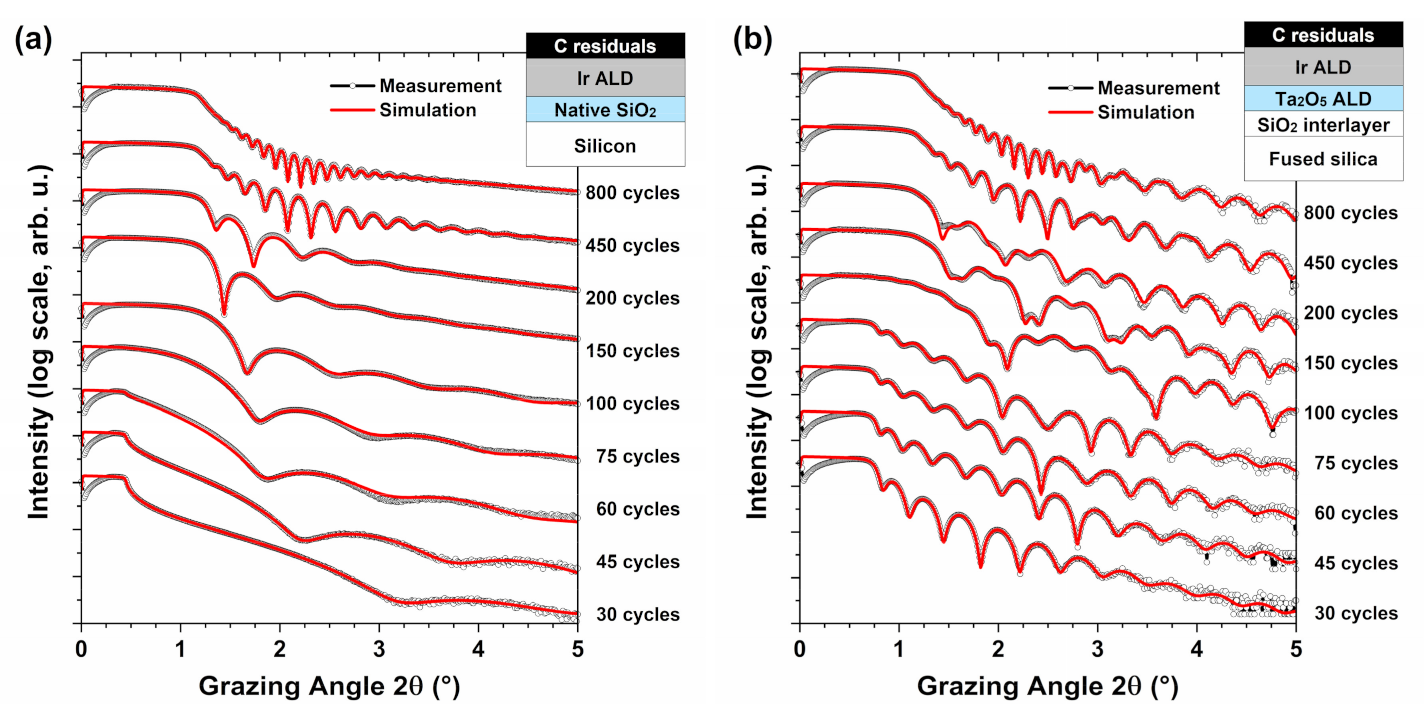
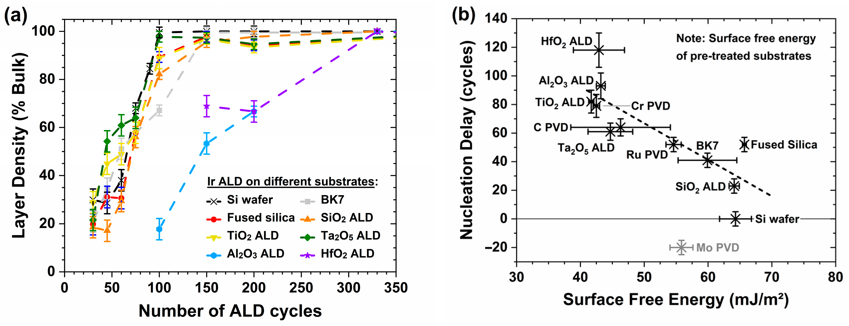
3.1. Nucleation of Iridium ALD Thin Films

In order to investigate the nucleation of iridium layers on different substrate materials, SEM images were obtained. Figure 1 shows top-view SEM images of Ir coatings depending on the number of ALD cycles on Si wafers, BK7, and fused silica, as well as seed layers of SiO2 ALD, Ta2O5 ALD, Al2O3 ALD, and C PVD. The number of ALD cycles was varied between 30 and 200 cycles. Due to charging effects of the SEM electron beam on isolating substrates, the image contrast is partly weak. However, the bright appearing Ir is clearly distinguishable from the substrates appearing dark.
ALD deposited Ir proceeds in the island growth mode (Volmer-Weber growth [45]) on all SEM investigated substrates and seed layers. As Figure 1 demonstrates, small Ir islands form on the substrate materials of Si wafers, BK7, fused silica, SiO2 ALD, Ta2O5 ALD, Al2O3 ALD und C PVD. The size, shape, and distribution of the individual islands vary on the different substrate materials. In the initial states of nucleation, the Ir islands have a diameter of several nanometers, which then continuously increases. Depending on the substrate material, nucleation may be delayed. Whether a thin wetting layer is present or not cannot be concluded unambiguously from these SEM images and is currently investigated to elucidate the growth mode within the first few ALD cycles of the deposition. Notably, the SEM analysis provides the snapshot of the film morphology ex-situ, after cooling and exposure to air, whereby changes due to the environment also cannot be excluded.
The nucleation and film growth of Ir on Si wafers shows the typical behavior of noble metals on dielectric surfaces. Small islands of Ir form on the substrate surface (30 cycles) and grow continuously. Due to liquid-like coalescence, neighboring islands touch and form larger particles (45–60 cycles). Consequently, the particle density decreases. Gradually, a coherent network forms (about 75–100 cycles), in which the remaining channels (after 100 cycles) and finally the holes (after 150 cycles) are filled up. On BK7 and the Ta2O5 ALD seed layers, the Ir nucleation behaves similarly. The Ir particles on BK7 are slightly smaller, and their particle density is higher. On Ta2O5, the nucleation appears slightly delayed, which is compensated by improved coverage of the surface. Finally, the Ir layers on Si wafers, BK7, and Ta2O5 ALD seed layers are almost fully closed after about 150–200 ALD cycles.
The layer formation of Ir on fused silica, SiO2 ALD, and C PVD is slightly inhibited compared to the above materials. On fused silica and SiO2 seed layers, tiny Ir islands are visible at 30 cycles. Due to charging effects of the SEM electron beam, the image contrast is very weak. However, on the C seed layer, these Ir islands are better visible. On fused silica, SiO2, and C, the density of Ir islands and coalesced particles is lower than on the Si wafers, BK7, and Ta2O5 seed layers. At about 100 cycles, a coherent network with relatively broad channels and large holes is present. These channels and holes close comparatively slowly. After 200 cycles, the Ir layers are almost closed, but channels and holes are still visible (dark areas in SEM images).
On the Al2O3 seed layers, the delayed nucleation of Ir is most prominent. After 30–45 cycles, no Ir islands are visible; after 60–75 cycles, small particles are sporadic. Only after 100 cycles, the Ir islands are significantly present, with coverage and particle density similar to SiO2 after 45 cycles. These particles grow and coalesce (about 150 cycles), but no coherent network is achieved after 200 cycles. At this stage, the Ir layers on the other substrate materials already have an almost closed layer.
Figure 2 shows the particle size distribution and surface coverage of Ir coatings exemplary on Si wafers and SiO2 ALD seed layers depending on the number of applied ALD cycles. The particle size and surface coverage were obtained from the SEM images using the image processing software ImageJ. Here, the distribution of the particle size is shown in combination with a box plot. The elements of the box plot are explained in Figure 2a. On Si wafers, the Ir islands have an average diameter of about 7.4 nm after 30 ALD cycles, as Figure 2a illustrates. The size of the particles increases continuously and achieves about 16 nm at 150 cycles. Nevertheless, the separation and size determination of several connected particles is hardly possible at this stage. The surface coverage on the Si wafers with Ir increases strongly and is about 91% at 100–150 cycles.
The particle size distribution and surface coverage of Ir coatings on SiO2 ALD seed layers depending on the number of ALD cycles is shown in Figure 2b. For 30 cycles, the average diameter of Ir particles is about 2.7 nm, with less than 1% surface coverage. The particle size increases continuously to about 10.7 nm at 75 cycles and about 22 nm at 150 cycles. However, the separation of connected particles and the determination of their size is difficult at this stage. The coverage of the SiO2 surface with Ir increases to about 50% at 75 cycles and about 82% at 150 cycles. Compared to the Si wafers, the Ir particles are about 6 nm (on average) larger at 150 cycles, but the surface coverage is about 10% lower.
To summarize, the nucleation of Ir layers on different substrate materials was investigated by SEM images. ALD deposited Ir forms an island growth mode, which is typical for noble metals on dielectric surfaces. The nucleation and layer formation of Ir on Si wafers, BK7, and Ta2O5 ALD seed layers behave similarly. On fused silica and seed layers of SiO2 ALD and C PVD, the layer formation is slightly inhibited. This delayed nucleation is very pronounced on Al2O3 seed layers.

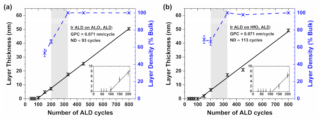
3.2. Growth of Iridium ALD Thin Films

After a detailed study of the nucleation, the growth of the iridium layers on different substrate materials was examined by XRR measurements. Figure 3 shows XRR measurements of Ir coatings with corresponding simulations with different numbers of ALD cycles exemplary on Si wafers and Ta2O5 seed layers. For clarity, the diffractograms are vertically shifted. The applied layer models for fitting the data are shown graphically, not true to scale.
With the applied layer models, the XRR measurements are fitted with very good agreement for the different substrate materials. For the correct fitting, the predefined layers were extended by one to three additional layers depending on the substrate material. For the Si wafers, a thin native SiO2 layer is considered on top of Si. For BK7 and fused silica, also a thin SiO2 interlayer is assumed between the bare substrates and the Ir or seed layers (except for SiO2 ALD seed layers). This interlayer is essential for the accurate description of the surface of the bare substrates. For the Mo PVD seed layers, oxidation of the molybdenum surface is considered by a thin MoO3 layer. On top of the Ir layers, a thin layer of carbon residuals (density about 2.0 g/cm3) of about 1–2 nm is assumed, similar to the study of Massahi et al. [46]. These carbon layers originate from the atmosphere and are crucial for simulating the ultra-thin Ir coatings. The thin Ir layers are not fully closed and consist of small metallic islands (see Figure 1). Using XRR, these metal-air mixtures are interpreted as closed layers with correspondingly reduced layer density or enhanced surface roughness of iridium. Figure 3 demonstrates that the XRR measurements of the Ir coatings with thicker layers (e.g., with 800 cycles) and thinner layers (e.g., with 45 cycles), as well as complex features (e.g., 100 cycles on Ta2O5 seed layer), are correctly reproduced. The Ir films, which reach bulk density as given by the XRR analysis, correspond to the coatings with a nearly closed Ir layer in the SEM images.
In Figure 4, Figure 5, Figure 6 and Figure 7, layer thicknesses and densities of the individual Ir layers on different substrate materials are shown as determined from the XRR analysis. From the linear fit of the film thickness in certain regions, the deposition rate as growth per cycle (GPC) and the nucleation delay (ND) until this linear growth starts, is calculated. For electrically non-conductive substrate materials, the region of percolation of the Ir layers was determined by four-point probe resistivity measurements. The GPC and ND for the Ir layers are indicated for all substrate materials, the region of percolation for the electrically non-conductive substrates.
The growth of Ir layers on Si wafers shows an overall linear layer thickness increase without ND; however, the layer density correlates to the island growth mode. As Figure 4a illustrates, the increase in layer thickness with the number of ALD cycles is linear with GPC = 0.071 nm/cycle, and no significant ND occurs. With the defined pulse and purge times for one Ir ALD cycle, this GPC corresponds to a deposition rate of about 0.057 nm/min or 3.44 nm/h. There are no differences identifiable for thinner or thicker Ir coatings. Within the first 100 cycles, the layer density increases strongly and reaches 100% of the Ir bulk density of 22.56 g/cm3 [47] after approx. 150 cycles. In order to exclude any influence of the sample position within the deposition chamber, all substrates always had an identical sample position in the deposition chamber within an area with a diameter of 150 mm. The layer thickness distribution within the deposition chamber is about 1.2% and 6.8% on areas with a diameter of 100 and 200 mm, respectively. The depositions were carried out simultaneously on all substrate materials to avoid any variation in process conditions.
For the film growth of Ir on BK7, three different regions are distinguishable: an initial regime, a transition regime, and a regime of thickness growth. Figure 4b shows a non-ideal growth behavior on BK7. The initial regime corresponds to the nucleation of the Ir layers (see Section 3.1) and extends to about 150 cycles. The film growth with GPC = 0.078 nm/cycle is approximately linear (red line), but an ND of about 27 cycles on BK7 exists. With an increasing number of ALD cycles, the layer density increases strongly. Percolation of the Ir layers, meaning the formation of a coherent network, occurs between 75 cycles and 100 cycles. This corresponds to about 3.1–5.2 nm layer thickness or layer density of about 58%–67% of the bulk material. When the linear film growth of the initial regime ends, the transition regime begins. In this transition regime, the nominal deposition rate seems to change, whereby the layer density is very close to the bulk material. Finally, the approximately linear regime (black line) of thickness growth starts at about 200 cycles. This thickness growth regime exhibits a GPC = 0.079 nm/cycle and ND of about 41 cycles. Thus, for this second linear regime, a second nucleation delay can be defined as well. The layer density in this regime equals the density of bulk material. The deposition rates for the two linear regimes differ only slightly but are significantly higher than expected from the layer thickness distribution within the deposition chamber.
Figure 5 shows that the Ir film growth on the substrate materials of fused silica, SiO2 ALD, TiO2 ALD, Ta2O5 ALD, Ru PVD, and Cr PVD also exhibits three different regimes. Depending on the substrate material, the values for GPC and ND differ in the linear initial and thickness growth regime, but the principle behavior is identical to BK7. Percolation of the Ir layers also occurs between 75 and 100 cycles. For the Ru and Cr seed layers, the region of percolation was not measurable. As on BK7, the transition regime between 100 and 150 cycles on SiO2 ALD seed layers is only weakly pronounced. The GPC for the regime of thickness growth is within the layer thickness distribution of the deposition chamber. For the Ir layers on fused silica, TiO2 ALD, Ta2O5 ALD, and Cr PVD, the beginning of the thickness growth regime is associated with a temporary decrease in layer density.
On Al2O3 and HfO2 seed layers, the nucleation and growth of the Ir ALD layers are significantly inhibited. As shown in Figure 6, the nucleation of Ir on the Al2O3 and HfO2 seed layers only starts between 75–100 cycles and 100–150 cycles, respectively. Consequently, the Ir layer percolation is delayed and occurs between 200 and 330 cycles. With about 330 cycles, the Ir layer exhibits bulk density, which is delayed by about 200 cycles compared to the other substrate materials. For the film growth of Ir on Al2O3 seed layers, no different regimes are identifiable; on the HfO2 seed layers, this is uncertain and needs further investigation. However, the increase in layer thickness with the number of ALD cycles is approximately linear, with GPC = 0.071 nm/cycle for both materials. The ND of Ir is most prominent on the Al2O3 and HfO2 seed layers with about 93 cycles and 113 cycles, respectively.
Dewetting of the Mo PVD seed layers leads to enhanced growth of Ir during the layer formation. The high substrate temperature of 380 °C during the Ir deposition causes the dewetting of Mo PVD seed layers [48]. In Figure 7a, a top-view SEM image with 75 cycles of Ir on a Mo seed layer is additionally shown. The large structures are molybdenum islands, while the very bright appearing dots are Ir islands, which cover the dark-appearing fused silica substrate and Mo islands. Due to the irregular and rough structure of the Mo islands, the thickness and density of the thinner Ir layers could not be analyzed. However, for thicker Ir coatings, the film growth is approximately linear, with GPC = 0.070 nm/cycle. In this case, a negative ND of about-20 cycles results, so the Ir growth during layer formation must be enhanced. This enhanced deposition rate could be caused by a higher reactivity of the Ir(acac)3 precursor combined with molybdenum or the increased surface area due to the Mo islands. The Ir layer density on Mo seed layers equals the bulk density.
The Ir film growth on C PVD seed layers also shows three different regimes with a very pronounced transition regime. In principle, the growth behavior of Ir on C seed layers is identical to BK7: a linear initial regime, a transition regime, and a linear regime of thickness growth. However, the transition regime between 150 and 200 cycles is very pronounced, with a decrease in layer density of about 20% of the bulk material. This temporary decrease of the Ir layer density is also present on fused silica, TiO2 ALD, Ta2O5 ALD, and Cr PVD, but less pronounced. Besides, the Ir layer thickness changes hardly in this transition regime and ranges between about 9.6–9.8 nm. This phenomenon occurs on the TiO2, Ru, and Cr seed layers between 150 and 200 cycles, too. For the Ru and Cr seed layer, the Ir layer thickness even decreases with an increasing number of ALD cycles. In this regime, probably the Ir nucleation is completed, and the holes and channels of the percolated layer are closing before the linear thickness growth starts. The surface roughness of the Ir layers also increases slightly. In order to understand the processes in this transition regime better, supplementary investigations are necessary.
On the metal oxide substrate surfaces, the density of the Ir layers increases strongly between 45 and 100 cycles, except on Al2O3 ALD and HfO2 ALD seed layer. Figure 8a shows that the Ir layer density on substrate materials of Si wafers, fused silica, SiO2 ALD, TiO2 ALD, and Ta2O5 ALD achieves at least about 82% of the bulk material within the first 100 cycles; on BK7, about 67%. For the Al2O3 ALD and HfO2 ALD seed layer, the Ir nucleation is delayed by about 100 cycles, and the formation of a dense Ir layer is significantly inhibited. With 200 cycles, these Ir layers exhibit a density of about 15.0 g/cm3 or about 67% of the bulk material. At the latest, with 330 cycles, which corresponds to 17.2–17.5 nm layer thickness, a closed and dense Ir layer is build.
The ND of Ir coatings in the linear regime of thickness growth correlates with the surface free energy of the corresponding substrate materials. As already described, the growth behavior and ND of Ir coatings depend strongly on the substrate material. Figure 8b shows the Ir ND of the thickness growth regime as a function of the surface free energy of the corresponding substrates with pre-treatment (see also Supplementary Table S4). Thereby, the pre-treatment imitates the Ir ALD deposition conditions for the bare substrates and seed layers. The higher the surface free energy of the substrate materials, the smaller the ND of the Ir layers and vice versa. In other words, the ND characteristic of ALD correlates with the wettability of the substrate materials. Seed layers of HfO2 ALD, Al2O3 ALD, TiO2 ALD, and Cr PVD show the lowest surface free energies and the largest ND of the Ir coatings. The Si wafers exhibit a surface free energy of about 64.3 mJ/m2 and a negligible ND. On the Mo PVD seed layers with a surface free energy of about 55.8 mJ/m2, the Ir growth is enhanced with a negative ND of about-20 cycles. However, the Mo seed layers are a special case because its surface dewets due to the high substrate temperature of 380 °C (see also Figure 7a). This relationship between the Ir ND of the thickness growth regime and surface free energy of the substrates is not strictly linear, but a correlation is clearly visible. The correlation persists for both the pre-treated and untreated substrate materials (see also Supplementary Figure S1). This correlation is only valid with the ND of the thickness growth regime and not the initial regime. However, the ND of the initial regime is implicitly included in the ND of the thickness growth regime.
For most substrate materials, the thickness of the Ir layers is precisely predictable using GPC and ND. As shown in detail, the ALD growth of Ir films is linear in certain regimes, so that a GPC and ND are derived for these regimes. The nominal thickness d of the Ir layers depending on the number of ALD cycles n is given as follows:
d = GPC (n − ND).
For non-closed Ir layers in the initial regime, which are interpreted as closed layers with correspondingly reduced layer density or enhanced surface roughness, this is an effective layer thickness. By considering the substrate material, sample position within the deposition chamber, and the condition of the ALD system, the Ir layer thickness in these linear growth regimes is achievable and reproducible with a deviation of less than 1 nm. However, Equation (1) is explicitly not valid for the non-linear transition regime.
The SEM images, XRR analysis, and four-point probe resistivity measurements on nucleation and film growth of Ir coatings are consistent with each other. The SEM images in Figure 1 matches approximately the calculated ND of the initial regime from the XRR analysis in Figure 4, Figure 5, Figure 6 and Figure 7. For instance, the ND of the initial regime on BK7 and C PVD seed layers is about 27 and 32 cycles, respectively. In the corresponding SEM images, iridium nucleation is initially visible at 30 cycles. On the Al2O3 ALD seed layers, an inhibited nucleation with an ND ≈ 93 cycles was observed. Their SEM images show that Ir islands occur sporadically from 60–75 cycles and are clearly present after 100 cycles. By using four-point probe measurements, percolation of the Ir coatings was determined between 75 and 100 cycles on all electrically non-conductive substrates, except for Al2O3 and HfO2. This transition from single and coalesced islands towards a coherent network with channels and holes is also traceable in the SEM images. The SEM images on Al2O3 also show that no percolated Ir layer is present after 200 cycles. The Ir layer density determined by XRR matches the SEM images in the initial regime up to 100 cycles. However, there are different results for the transition regime or almost closed Ir layers. For example, the Ir layer density on Si wafers achieves bulk density after about 100 cycles (see also Figure 8a). Nevertheless, narrow channels and holes are still visible in the corresponding SEM images. In this case, the almost closed Ir layers are interpreted effectively as closed layers with bulk density but slightly increased surface roughness. Thus, the channels and holes are interpreted as increased surface roughness and not as reduced layer density. However, this effect and the resulting differences are relatively small and mainly independent of the determined effective layer thickness. For analysis of the film formation, XRR is a convenient method but needs complementary methods in the transition regime, such as SEM images.
To summarize, the growth of Ir layers on different substrate materials was examined by XRR measurements. A lower Ir layer density is determined for all investigated substrate types in the first 100–330 cycles depending on the seed layer. This lower density correlates with the island growth type, while the complete surface coverage agrees to the formation of layers with near bulk material density. On Si wafers, the growth is overall linear and without nucleation delay. For the film growth on BK7 and fused silica as well as seed layers of SiO2 ALD, TiO2 ALD, Ta2O5 ALD, Ru PVD, Cr PVD, and C PVD, three different regions are distinguishable: a linear initial regime, a non-linear transition regime, and a linear regime of thickness growth. On the metal oxide substrate surfaces, the Ir layer density increases strongly between 45 and 100 cycles. In contrast, for Al2O3 and HfO2 seed layers, the Ir nucleation is significantly delayed, and the formation of a dense layer is inhibited. Dewetting of Mo PVD seed layers, caused by the high substrate temperature of 380 °C, leads to enhanced Ir growth during the layer formation. For the linear regime of thickness growth, the ND of Ir coatings correlates with the surface free energy of the corresponding substrates. The thickness of Ir layers on most substrate materials is precisely predictable using GPC and ND. The XRR analysis, four-point probe resistivity measurements, and SEM images are consistent with each other.

3.3. Properties of Iridium ALD Thin Films

After studying the nucleation and film growth, the properties of iridium layers grown on different substrate materials are examined. The surface roughness, size of the Ir crystallites, specific electrical resistance, adhesion to the substrate, and elemental composition were determined. Figure 9 shows AFM images of thicker Ir coatings with 800 ALD cycles, which corresponds to a 50–60 nm layer thickness, on different substrate materials. For all images, the root-mean-square (rms) surface roughness of these 2 × 2 µm2 sample areas is calculated.
The topography of thicker Ir layers on the different substrate materials is homogeneous and smooth with a surface roughness of about 1.0–1.7 nm rms, except for BK7, TiO2 ALD, and HfO2 ALD. On the Si wafer, the surface roughness of the Ir layer is lowest with about 1.0 nm rms. Because the surface of the bare Si wafer is very smooth (surface roughness about 0.15 nm rms), probably the surface roughness of the Ir layer is determined only by the Ir nucleation on the Si wafer. The Ir layers on the PVD seed layers of Cr, Mo, and C exhibits a surface roughness of about 1.1 nm rms. On the Mo seed layer, the Ir surface roughness is in the range of the bare Mo seed layer itself. With about 1.2 nm rms, Ta2O5 shows the lowest Ir surface roughness of the evaluated metal oxide seed layers. The Ir layers on fused silica and SiO2 ALD, chemically both SiO2, shows a surface roughness of about 1.3 nm rms. On the PVD deposited Ru seed layer, the Ir surface roughness is about 1.4 nm rms. The roughness on the Al2O3 seed layer is about 1.7 nm rms, which is the highest value for the coatings with a homogeneous topography.
For the Ir layer on BK7, the irregular topography is caused by the substrate material itself. In Figure 9, the AFM image of the Ir layer on BK7 shows small trenches or valleys, which are conformally overcoated with iridium. These valleys are already present on the bare BK7 substrate with a surface roughness of about 1.9 nm rms. In combination with the Ir layer, this results in a surface roughness of about 2.1 nm rms. Hence, the main contribution to the surface roughness of the Ir coating on BK7 comes from the substrate itself and not the coating.
Crystallization of the TiO2 seed layer causes areas of lower and higher Ir surface roughness. The Ir layer on the TiO2 seed layer has an irregularly limited surface structure. These structures are identifiable using AFM and SEM and have an elongation of about 0.4 µm up to 6 µm. Due to the high deposition temperature of 380 °C for iridium, the 20 nm thin TiO2 seed layer crystallizes [49,50]. Probably, the irregularly limited structures represent differently oriented crystallites of the underlying TiO2 seed layer. Using XRD, only the crystallographic TiO2(101) plane of the TiO2 anatase phase is detectable (see also Supplementary Figure S2). Unfortunately, it is unclear which orientation of the TiO2 crystallites could cause the areas of different surface roughness. In the areas of lower and higher surface roughness, the Ir surface roughness is about 1.2 and 1.9 nm rms, respectively. On average, the surface roughness of the Ir layer on the TiO2 seed layer is relatively low at about 1.6 nm rms.
Crystallization of the HfO2 seed layer leads to smaller and larger hillocks and high surface roughness of the Ir coating. Hillocks are characteristic for the crystallization of HfO2 layers at higher temperatures [51]. However, due to the small thickness of the HfO2 seed layer, their crystallization is not detected by XRD. Here, the hillocks are partly over 100 nm in height and cause the high surface roughness of the Ir coating of about 4.6 nm rms. Consequently, the main contribution to the surface roughness comes from the HfO2 seed layer and not the Ir layer.
The layer properties of Ir coatings on different substrate materials are summarized in Table 1. For each substrate material, the AFM surface roughness (from Figure 9), estimated crystallite size, and specific electrical resistance is obtained from thicker Ir coatings with 800 ALD cycles, which corresponds to a layer thickness of 50–60 nm. Additionally, the specific electrical resistance for thinner coatings with 150 cycles (330 cycles on Al2O3, HfO2, and Mo seed layers marked with an asterisk) is given. The qualitative results of tape tests, according to DIN ISO 92211-4 [44], are obtained from Ir coatings with 330 cycles. These material properties show no significant correlations to one another.
The Ir ALD coatings exhibit an average crystallite size of about 30 nm and show a preferred orientation of the crystallographic Ir(111) plane (see also Supplementary Figure S2). Using Scherrer’s equation, the size of the Ir crystallites was estimated from the most intense Ir(111) diffraction peak. The smallest Ir crystallites form on the HfO2 seed layer with about 27 nm, the largest on fused silica with about 34 nm. For a randomly oriented Ir powder sample, the two most intense diffraction peaks, Ir(111) and Ir(200), have a ratio of I(111)/I(200) = 2 [52]. Here, the ratio I(111)/I(200) of the Ir coatings varies between about 6 on the HfO2 seed layer and 122 on the Si wafer (see also Supplementary Table S5). Consequently, the crystallographic Ir(111) plane is preferred, also compared to all other phases in the Ir layers. Aaltonen et al. observed that the preferred Ir(111) orientation even increases with increasing deposition temperature [23]. However, there is no significant correlation between the preferred Ir(111) orientation and the size of the Ir crystallites.
The specific electrical resistance of Ir coatings with 800 cycles on different substrate materials ranges between 7.7 × 10⁻⁸ and 14.5 × 10⁻⁸ Ω·m. For Ir coatings on the TiO2 seed layer, the lowest specific electrical resistance (best electrical conductivity) with about 7.7 × 10⁻⁸ Ω·m is obtained. This could be related to the irregular topography of the Ir layer with areas of lower and higher surface roughness. On the PVD seed layers of Cr and Mo, the coatings exhibit the highest specific electrical resistance (worst electrical conductivity) with about 14.4 × 10⁻⁸ and 14.5 × 10⁻⁸ Ω·m, respectively. For the metallic seed layer, their thickness is also included in calculating the specific electrical resistance. On average, the specific electrical resistance is about 10.3 × 10⁻⁸ Ω·m, which is comparable to other studies [53] and relatively close to the value for bulk material of 4.7 × 10⁻⁸ Ω·m [54].
The specific electrical resistance of thinner Ir coatings (150 and 330 cycles) is significantly higher compared to the thicker coatings and depends strongly on the substrate material. For thinner Ir coatings, the lowest specific electrical resistances are obtained on the Si wafer and TiO2 ALD seed layer with about 13.0 × 10⁻⁸ and 13.2 × 10⁻⁸ Ω·m, respectively. The highest specific electrical resistance exhibits Ir on the Cr PVD seed layer with about 40.0 × 10⁻⁸ Ω·m. Compared to the thicker Ir coatings, the values spread more widely and, in some cases, differ strongly depending on the seed material. The deposition of high quality ultra-thin metallic layers with a film thickness below 10 nm is critical for numerous optical and electrical applications. The choice of a seed material must be carefully considered since the properties of ultrathin metallic layers depend significantly on the surface chemistry. Further analysis of the optical properties is currently in progress.
Adhesion tests show that the Ir coatings are adhesive only on the substrate materials of Al2O3 ALD, Cr PVD, and C PVD. Even after performing the tape test twice at the same sample position, the Ir layers were not peeled off. The Ir layers on the PVD deposited seed layers of Ru and Mo were partially delaminated from the substrate. For all other substrate materials (Si wafer, BK7, fused silica, SiO2, TiO2, Ta2O5, and HfO2), the Ir layers were removed completely from the substrate using a tape test. The metal oxide seed layers themselves are adhesive to their fused silica substrates. Thus, the Ir layers were peeled off the metal oxide seed layers and not the underlying fused silica substrates. Nevertheless, all Ir layers adhere to their substrate materials without mechanical influence and do not delaminate by themselves.
The Ir layers contain less than 1% impurities of oxygen and carbon. Figure 10 shows an AES depth profile of an Ir coating on a Si wafer, where the atomic ratios are plotted as a function of the sputtering time. On the surface (sputtering time = 0 s), the Ir layer consists of about 95.5% iridium, 3.5% carbon, and 1% oxygen. This relatively high percentage of carbon on the surface originates from contact with the atmosphere. In the Ir layer, the iridium content increases to over 99%, and the total content of impurities (oxygen and carbon) decreases below 1%. Mattinen et al. reported comparable results for the same ALD process. [53]. This means that the Ir ALD process runs efficiently, the acetylacetonate ligands are reduced completely, and excess precursors and reaction products are removed entirely from the deposition chamber. At a sputtering time of about 200 s, the interface to the Si wafer as substrate material is reached. No other elements than iridium, carbon, oxygen, and silicon were detectable. It is assumed that the elemental composition of the Ir layers is identical for all substrate materials.
To conclude, the surface of thicker Ir layers is homogeneous and smooth, except for the substrate materials of BK7, TiO2 ALD, and HfO2 ALD. For Ir layers on BK7, TiO2, and HfO2, the substrate itself, respectively, crystallization of the seed layers causes an irregular topography. The Ir layers show a preferred Ir(111) orientation with an average crystallite size of about 30 nm. For thicker Ir coatings, the specific electrical resistance ranges between 7.7 × 10⁻⁸ and 14.5 × 10⁻⁸ Ω·m, which is relatively close to the value for the bulk material. For thinner coatings, these values are significantly higher and depend strongly on the substrate material. Only the Ir coatings on Al2O3 ALD, Cr PVD, and C PVD seed layers are adhesive to their substrates using a tape test. In the Ir layers, less than 1% impurities of oxygen and carbon are contained.

4. Discussion

As thin-film material, the noble metal iridium is essential for numerous applications. With ALD also complex shaped or micro-structured substrates are conformally and homogeneously coatable. However, the Ir layer properties, especially of very thin layers, depend strongly on the substrate material. The nucleation, film growth, and properties of Ir coatings are extensively discussed here on various substrate materials. Based on these results, substrate materials are specifically selectable to tailor the properties of Ir coatings for different applications.
Iridium forms an island growth mode on the SEM investigated substrate materials of Si wafers, BK7, fused silica, SiO2 ALD, Ta2O5 ALD, Al2O3 ALD, and C PVD. On these substrate materials, the size, shape, and distribution of individual islands vary, as Figure 1 illustrates. As an example, Figure 2 shows the particle size distribution and surface coverage of Ir on Si wafers and SiO2 ALD seed layers depending on the number of ALD cycles. However, the fundamental growth mode is the same and typical for noble metals on dielectric surfaces [45,55]. Mattinen et al. investigated the nucleation of Ir by ALD using Ir(acac)3 and different co-reactants of air, O2, consecutive O2 and hydrogen (H2), and consecutive ozone (O3) and H2 [29]. Although the GPC and ND changed with the different ALD processes, the Ir coatings always exhibited island growth. Other studies on the deposition of Ir by ALD [23,26,56,57], chemical vapor deposition [58,59], evaporation [60,61], or a facile one-pot solvothermal method [62] show comparable results. However, these studies were performed with relatively thick Ir layers, with SEM images providing reliable information for several tens of ALD cycles. The atomic-level interactions within the first cycles cannot be concluded yet and are currently investigated.
Island growth of the Ir coatings shows different characteristics depending on the substrate material, as Figure 4, Figure 5, Figure 6 and Figure 7 illustrates. This XRR analysis is consistent with the SEM images (Figure 1) and four-point probe resistivity (Table 1) measurements. For the nucleation and film growth on Si wafers, no differences occur for thinner or thicker Ir coatings. With an increasing number of ALD cycles, the Ir layer thickness increases linearly without ND; consequently, the GPC is constant. In contrast, on the substrate materials of BK7, fused silica, SiO2, TiO2, Ta2O5, Ru, Cr, and C, three different regions are distinguishable: a linear initial regime, a non-linear transition regime, and a linear regime of thickness growth. For these substrate materials, the GPC of the initial regime differs significantly from the GPC of the thickness growth regime. On the metal oxide substrate surfaces of fused silica, SiO2, TiO2, and Ta2O5, the GPC of the initial regime is lower; on the seed layer of Ru, Cr, and C, the GPC is higher. In the case of Mo seed layers, the Ir layer thickness for thinner coatings was not determinable. However, for thicker Ir coatings, a negative ND was calculated, caused by an enhanced Ir growth during the layer formation.
The model for island growth of ALD deposited coatings agrees partially with these results for Ir coatings. Puurunen et al. proposed four classes of ALD processes based on the GPC variation with the number of ALD cycles: a linear growth, substrate-enhanced growth, and a substrate-inhibited growth of type 1 and type 2 [63]. Island growth is described as substrate-inhibited growth of type 2, where the GPC first increases, passes through a maximum, and finally settles to a constant value. According to Alam & Green, these three regions are designated as the initial regime, transition regime, and linear regime [64]. Notwithstanding, in this article, the third regime is called the thickness growth regime since this regime is related to the thickness growth of the Ir layer, and the initial regime is also considered linear. In principle, this classification agrees with the Ir growth behavior on BK7, fused silica, SiO2, TiO2, Ta2O5, Ru, Cr, and C. Their GPC of the thickness growth regime is linear and constant. For the transition regime, their GPC exhibits a maximum (or inflection point) so that the GPC of initial and thickness growth regime continuously merge. However, in the initial regime, the GPC should increase with an increasing number of ALD cycles. Here, the Ir layer thickness linearly increases, and therefore the GPC is constant. Nevertheless, Alam & Green noted that film growth in the initial regime could be linear or non-linear, depending on the pre-treatment of the substrate [64]. However, the island growth of Ir on Si wafers seems to proceed overall linear and belongs to the class of linear growth. In the case of Mo seed layers, the ND is negative, which indicates the class of substrate-enhanced growth. Altogether, the substrate material (and its pre-treatment) seems to determine the growth mode of the coating material for given process parameters.
The ND of Ir ALD coatings correlates with the surface free energy of the corresponding substrate materials. As Figure 8b illustrates, the ND determined from the thickness growth regime decreases with an increasing surface free energy of the substrate. This observed relationship is not strictly linear, but the trend is clearly visible for both pre-treated and untreated substrates. A few reports on PVD thin films relate the influence of seed layers on film growth and morphology to the surface free energy [65]. Kitakami et al. explained the crystallographic texture of sputtered Co films depending on their underlayer with the difference in surface free energy between the Co film and underlayer material [66]. Chen et al. investigated the degree of perpendicular magnetic anisotropy (PMA) of sputtered Co80Pt20 films deposited on Ru/Cu bilayers and pure Cu layers [67]. Similarly, the authors consider the surface free energy as one main reason for the PMA degree depending on the underlayer. Recently, Stempfhuber et al. improved the topography and optical properties of sputtered Al films using Ti and Cu seed layers [68]. The authors explain their results, including the difference in free surface energy between the Al film and the seed layer, but also based on stronger bondings between Al-Ti than Al-Cu.
The ND of ALD-deposited thin films has not been associated with the surface free energy of their substrate materials yet. According to the capillary theory of film growth, layer-by-layer growth occurs for γS ≥ γSF + γF with the surface free energy (γ) of the substrate (S) surface, substrate/film (SF) interface, and film (F) surface [69]. Additionally, the surface free energy of the substrate depends on their pre-treatment and temperature conditions [70]. Although the determination of the surface free energy with deionized water under ambient conditions represents a coarse approximation of the deposition conditions, a good correlation between the surface free energy and ND is observed. With increasing surface free energy of the substrate, the wettability of this surface increases, and more Ir is bound to the substrate surface resulting in a lower nucleation delay. The bonding of Ir(acac)3 precursor and intermediate species on the substrate surface is critical in the first ALD cycles. The reaction between the precursor and Ir islands proceeds more efficiently, leading to more deposited material on pre-existing Ir islands than on bare substrates or seed layers (except on Si wafers and Mo seed layers). Consequently, a strong substrate-inhibited growth leads to large and isolated Ir islands, as observed on Al2O3 seed layers. The reaction sites on a substrate surface indeed vary with the substrate material. Aware that other effects, such as surface diffusion [71] and bonding energy [72], influence the nucleation behavior, the correlation between the surface free energy and ND is significant. However, little data is available on these particular material-specific parameters and material combinations. Enhanced surface diffusion of Ir adatoms or clusters could also favor the formation of islands and a delayed percolation of the layer [65].
The substrate material determines the growth mode and growth regime boundaries of the Ir layers. In the thickness growth regime, the linear thickness growth of the (almost) closed Ir layer starts. The GPC is constant and corresponds to the Ir ALD growth on an Ir surface. For this regime, the ND correlates with the surface free energy of the (untreated and pre-treated) substrate material, meaning the wettability of the substrate. The initial regime is related to island formation, coalescence, and percolation of the Ir layers. With an increasing number of ALD cycles, the effective layer thickness increases linearly, but an ND can occur. GPC and ND of the initial regime are determined by the reactivity of the precursors with the substrate surface compared to iridium. On Si wafers, no growth differences appear, so the Ir growth is overall linear, and no transition regime occurs for this substrate material. On fused silica, SiO2, TiO2, and Ta2O5, the initial growth of Ir is inhibited. Consequently, the GPC is lower compared to the thickness growth regime in combination with a possibly present ND. In contrast, on Ru, Cr, and C seed layers, the initial Ir growth seems slightly enhanced on these substrate surfaces. After a few conditioning Ir ALD cycles (ND = 24–34 cycles), the GPC is higher compared to the thickness growth regime. The transition regime represents the transition from a percolated to an (almost) closed Ir layer. Thereby, the GPC of the initial regime continuously converges to the GPC of the thickness growth regime. The manifestation of the transition regime depends on the differences in GPC and ND between the initial and thickness growth regime. For instance, on BK7, the differences in GPC (0.078 and 0.079 nm/cycle) and ND (27 and 41 cycles) are relatively small, so the transition regime is weakly pronounced.
Numerous publications report about the influence of process parameters on layer properties but hardly consider the substrate material. Many studies investigate the effect of process parameters on specific layer properties, e.g., for ALD deposited metals of Co [73], Cu [74], and Ru, Pd, and Pt [75]. However, only a few studies also consider the influence of substrate materials and seed layers or the nucleation and film growth of ALD deposited layers, e.g., for Cu [76], Pd [77], W [78], Pt [79,80,81], StTiO3 [82], CuOx [83], and Al2O3, HfO2, Ta2O5, and TaNx [84]. Lui et al. investigated the nucleation of Ir nano-crystals on in-situ and ex-situ ALD-grown Al2O3 layers [57]. The authors found out that nucleation on ex-situ deposited Al2O3 is strongly inhibited compared to the in-situ deposition, which is consistent with results in this study. However, the in-situ deposition of different coating materials is not always possible. For instance, when the substrate temperatures for the ALD-deposition are very different, or the coating materials are not available by ALD.
The targeted selection of substrate materials or their suitable pre-treatment can tailor the properties of Ir coatings for particular applications. For instance, a seed layer material that exhibits a low ND (e.g., Ta2O5 seed layer) would enable ultrathin, dense conductive layers. In contrast, a large ND (e.g., Al2O3 seed layer) would prevent certain areas from the deposition as in area-selective ALD processes and the formation of very small nanoparticles. By considering the surface free energy of the substrates, the corresponding ND of Ir is readily assessable. Furthermore, adhesive, smooth, and highly reflective Ir mirrors for the deep ultra-violet or X-ray spectral range require Cr or C seed layers (see Table 1) [12]. In particular, Cr serves as an adhesion layer for numerous coating materials and is available by magnetron sputtering in high quality. On micro-structured substrates, conformal Al2O3 seed layers are necessary for adhesive Ir coatings. Especially, Al2O3 by ALD using trimethylaluminum (TMA) and H2O is a common ALD material, which is conformally coatable in a broad temperature range. Thus, temperature-sensitive materials (e.g., polymers, structured photoresist) can be protected before the Ir ALD deposition [10] or in-vacuo mixtures of Al2O3 and Ir are possible. However, iridium layers on Al2O3 seed layers need further optimization because they suffer from an inhibited nucleation and increased surface roughness. For the fabrication of very thin Ir coatings, seed layers of Ta2O5 are more suitable. After 100 cycles, the Ir layers exhibit a thickness of about 5.3 nm and are almost fully closed but not adhesive to the Ta2O5 seed layer. The deposition of ultra-thin, high-quality Ir films and metals, in general, is limited by island formation. The choice of proper seed materials is critical in achieving such coatings. Furthermore, chemical wet etching of Si with Ir nanoparticles forms a nanoporous sponge-like Si structure, as recently demonstrated [85]. Small and homogenously distributed Ir islands form on Si wafers, with particle size and distribution controlled by the number of ALD cycles (see Figure 1), which serve as catalytic sites. Another possibility to influence the layer properties or growth mode is a suitable pre-treatment of the substrate material. Lee et al. changed the growth mode of ALD deposited TiO2 films by modifying the surface free energy of Si substrates using mixed self-assembled monolayers [86]. Additionally, a study of the influence of the metalorganic precursor on the growth on different seed layer materials is necessary to further clarify the relationship between wettability, chemical reactions, and surface diffusion on the Ir metal growth.

5. Conclusions

In conclusion, iridium thin films were prepared by ALD on Si wafers, BK7, and fused silica as well as seed layers of SiO2, TiO2, Ta2O5, Al2O3, HfO2, Ru, Cr, Mo, and C. Their nucleation, film growth, and properties were investigated by SEM, XRR, XRD, four-point probe resistivity measurements, contact angle measurements, AFM, tape tests, and AES. Iridium forms an island growth mode on these substrate materials, which is typical for noble metals on dielectric surfaces. However, this island growth shows different characteristics depending on the substrate material and leads to differences in the film properties of ultra-thin layers. For Ir on Si wafers, the growth is overall linear and without a nucleation delay. On BK7, fused silica, SiO2, TiO2, Ta2O5, Ru, Cr, and C, three different regions are distinguishable: a linear initial regime, a non-linear transition regime, and a linear regime of thickness growth. The thickness growth regime corresponds to the thickness growth of Ir ALD on an (almost) closed Ir surface. The initial regime represents the initial Ir layer formation, whereby both regimes merge continuously over the transition regime. The Ir nucleation and film formation on Al2O3 and HfO2 is significantly inhibited. Dewetting of Mo causes an enhanced Ir growth during the layer formation. For these substrate materials, the ND of the Ir coatings could be associated with the surface free energy of the corresponding substrates. Besides, the effective Ir layer thickness is precisely predictable on most substrate materials using GPC and ND. The surface of thick Ir coatings is homogeneous and smooth, except on BK7, TiO2, HfO2. For these coatings, the substrate itself and crystallization of the seed layers cause an irregular topography. All thick Ir coatings exhibit bulk density, a preferred orientation of the crystallographic Ir(111) plane, and specific electrical resistance close to the bulk material value. For thinner coatings, the specific electrical resistance is significantly higher and depends strongly on the substrate material. In this study, the lowest film thickness of a closed Ir layer is about 5 nm obtained with a Ta2O5 seed layer. Unfortunately, only Ir coatings on Al2O3, Cr, and C are adhesive to their substrates using a tape test. The Ir layers contain less than 1% impurities in total. By targeted selection of the seed material, the properties of Ir coatings are tailorable for particular applications.

Supplementary Materials

The following are available online at https://www.mdpi.com/2079-6412/11/2/173/s1, Table S1: Process parameters for the metal oxide seed layers grown by atomic layer deposition (ALD), Table S2: Process parameter for the seed layers grown by physical vapor deposition (PVD), Table S3: Properties of the bare substrates and seed layers before the iridium (Ir) deposition, Table S4: Equilibrium contact angle and calculated surface free energy of untreated and pre-treated substrate materials before the Ir deposition, Table S5: X-ray diffraction peak ratios of Ir coatings on different substrate materials and a powder reference sample, Figure S1: Iridium nucleation delay (ND) of thickness growth regime correlates with the surface free energy of the corresponding (untreated) substrate materials, Figure S2: X-ray diffraction (XRD) pattern of Ir coatings (with 800 cycles corresponding to 50–60 nm layer thickness) on different substrate materials.

Author Contributions

Conceptualization, P.S. and A.V.S.; methodology, P.S. and A.V.S.; formal analysis, P.S., V.B., N.F., P.P. and F.O.; investigation, P.S.; writing—original draft preparation, P.S.; writing—review and editing, P.S., T.F. and A.V.S.; visualization, P.S.; supervision, A.V.S.; project administration, A.V.S. and A.T.; funding acquisition, A.V.S. and A.T. All authors have read and agreed to the published version of the manuscript.

Funding

This research was funded by the Fraunhofer Society Attract Project (grant number 066-601020), Fraunhofer IOF Center of Excellence in Photonics, and Deutsche Forschungsgemeinschaft (DFG, German Research Foundation) Sonderforschungsbereich SFB 1375 “NOA—Nonlinear Optics down to Atomic scales”—project number 398816777.

Institutional Review Board Statement

Not applicable.

Informed Consent Statement

Not applicable.

Data Availability Statement

Data is contained within the article and supplementary material. Additional data presented in this study are available on request from the corresponding author.

Acknowledgments

The authors thank David Kästner for technical support, Thomas Müller, Michael Scheler, and Kristin Pfeiffer for the seed layer preparation, Lisa Vogt for contact angle measurements, and Silke Frunzke for the AES measurement, as well as Lilit Ghazaryan for helpful corrections. Especially, the authors thank Natali Sergeev for the laborious preparation of all SEM images. We also acknowledge the reviewers for their constructive comments to improve this article.

Conflicts of Interest

The authors declare no conflict of interest. The funders had no role in the design of the study; in the collection, analyses, or interpretation of data; in the writing of the manuscript, or in the decision to publish the results.

References

  1. Larruquert, J.I.; Mendez, J.A.; Aznarez, J.A. Non-oxidized Al-overcoated Ir bilayers with high reflectance in the extreme ultraviolet above 50 nm. Opt. Eng. 2002, 41, 1418–1424. [Google Scholar] [CrossRef] [Green Version]
  2. Kovacs, G.T.A.; Storment, C.W.; Kounaves, S.P. Microfabricated heavy metal ion sensor. Sens. Actuators B Chem. 1995, 23, 41–47. [Google Scholar] [CrossRef]
  3. Briand, D.; van der Schoot, B.; de Rooij, N.F.; Sundgren, H.; Lundstrom, I. A low-power micromachined MOSFET gas sensor. J. Microelectromech. Syst. 2000, 9, 303–308. [Google Scholar] [CrossRef]
  4. Andersson, P.G. Iridium Catalysis; Springer: Berlin/Heidelberg, Germany, 2011; ISBN 978-3-642-15334-1. [Google Scholar]
  5. Sawy, E.N.E.; Birss, V.I. Nano-porous iridium and iridium oxide thin films formed by high efficiency electrodeposition. J. Mater. Chem. 2009, 19, 8244–8252. [Google Scholar] [CrossRef]
  6. Shirvaliloo, S.; Kangarloo, H. Production of iridium metal thin films for application as electrodes in DRAMs and FRAMs. J. Electr. Electron. Eng. 2014, 3, 35–38. [Google Scholar] [CrossRef]
  7. Igumenov, I.K.; Gelfond, N.V.; Galkin, P.S.; Morozova, N.B.; Fedotova, N.E.; Zharkova, G.I.; Shipachev, V.I.; Reznikova, E.F.; Ryabtsev, A.D.; Kotsupalo, N.P.; et al. Corrosion testing of platinum metals CVD coated titanium anodes in seawater-simulated solutions. Desalination 2001, 136, 273–280. [Google Scholar] [CrossRef]
  8. Hemphill, R.; Hurwitz, M.; Pelizzo, M.G. Osmium atomic-oxygen protection by an iridium overcoat for increased extreme-ultraviolet grating efficiency. Appl. Opt. 2003, 42, 5149–5157. [Google Scholar] [CrossRef]
  9. Kajiwara, M.; Uemiya, S.; Kojima, T.; Kikuchi, E. Rhodium- and iridium-dispersed porous alumina membranes and their hydrogen permeation properties. Catal. Today 2000, 56, 83–87. [Google Scholar] [CrossRef]
  10. Weber, T.; Käsebier, T.; Szeghalmi, A.; Knez, M.; Kley, E.-B.; Tünnermann, A. Iridium wire grid polarizer fabricated using atomic layer deposition. Nanoscale Res. Lett. 2011, 6, 558. [Google Scholar] [CrossRef] [Green Version]
  11. Vila-Comamala, J.; Gorelick, S.; Färm, E.; Kewish, C.M.; Diaz, A.; Barrett, R.; Guzenko, V.A.; Ritala, M.; David, C. Ultra-high resolution zone-doubled diffractive X-ray optics for the multi-keV regime. Opt. Express 2011, 19, 175–184. [Google Scholar] [CrossRef] [Green Version]
  12. Probst, A.-C.; Begou, T.; Döhring, T.; Zeising, S.; Stollenwerk, M.; Stadtmüller, J.; Emmerich, F.; Lumeau, J. Coating stress analysis and compensation for iridium-based X-ray mirrors. Appl. Opt. 2018, 57, 8775–8779. [Google Scholar] [CrossRef] [PubMed]
  13. Suntola, T. Atomic layer epitaxy. Mater. Sci. Rep. 1989, 4, 261–312. [Google Scholar] [CrossRef]
  14. Ritala, M.; Leskelä, M. Chapter 2-Atomic layer deposition. In Handbook of Thin Films; Nalwa, H.S., Ed.; Academic Press: Burlington, MA, USA, 2002; pp. 103–159. ISBN 978-0-12-512908-4. [Google Scholar]
  15. Aaltonen, T.; Alén, P.; Ritala, M.; Leskelä, M. Ruthenium thin films grown by atomic layer deposition. Chem. Vap. Depos. 2003, 9, 45–49. [Google Scholar] [CrossRef]
  16. Aaltonen, T.; Ritala, M.; Leskelä, M. ALD of Rhodium thin films from Rh(acac)3 and oxygen. Electrochem. Solid-State Lett. 2005, 8, C99–C101. [Google Scholar] [CrossRef]
  17. Lashdaf, M.; Hatanpää, T.; Krause, A.O.I.; Lahtinen, J.; Lindblad, M.; Tiitta, M. Deposition of palladium and ruthenium β-diketonates on alumina and silica supports in gas and liquid phase. Appl. Catal. A 2003, 241, 51–63. [Google Scholar] [CrossRef]
  18. Niskanen, A.; Hatanpää, T.; Arstila, K.; Leskelä, M.; Ritala, M. Radical-enhanced atomic layer deposition of silver thin films using phosphine-adducted silver carboxylates. Chem. Vap. Depos. 2007, 13, 408–413. [Google Scholar] [CrossRef]
  19. Hämäläinen, J.; Sajavaara, T.; Puukilainen, E.; Ritala, M.; Leskelä, M. Atomic layer deposition of osmium. Chem. Mater. 2012, 24, 55–60. [Google Scholar] [CrossRef]
  20. Aaltonen, T.; Ritala, M.; Sajavaara, T.; Keinonen, J.; Leskelä, M. Atomic layer deposition of platinum thin films. Chem. Mater. 2003, 15, 1924–1928. [Google Scholar] [CrossRef]
  21. Griffiths, M.B.E.; Pallister, P.J.; Mandia, D.J.; Barry, S.T. Atomic layer deposition of gold metal. Chem. Mater. 2016, 28, 44–46. [Google Scholar] [CrossRef]
  22. ALD Database. Available online: www.atomiclimits.com/alddatabase (accessed on 15 October 2020).
  23. Aaltonen, T.; Ritala, M.; Sammelselg, V.; Leskelä, M. Atomic layer deposition of iridium thin films. J. Electrochem. Soc. 2004, 151, G489–G492. [Google Scholar] [CrossRef]
  24. Dussarrat, C.; Gatineau, J. High purity iridium thin films depositions using the inorganic IrF6. Proc. Electrochem. Soc. 2005, 5, 354–359. [Google Scholar]
  25. Kim, S.-W.; Kwon, S.-H.; Kwak, D.-K.; Kang, S.-W. Phase control of iridium and iridium oxide thin films in atomic layer deposition. J. Appl. Phys. 2008, 103, 23517. [Google Scholar] [CrossRef] [Green Version]
  26. Hämäläinen, J.; Hatanpää, T.; Puukilainen, E.; Costelle, L.; Pilvi, T.; Ritala, M.; Leskelä, M. (MeCp)Ir(CHD) and molecular oxygen as precursors in atomic layer deposition of iridium. J. Mater. Chem. 2010, 20, 7669–7675. [Google Scholar] [CrossRef]
  27. Schlicht, S.; Haschke, S.; Mikhailovskii, V.; Manshina, A.; Bachmann, J. Highly reversible water oxidation at ordered nanoporous iridium electrodes based on an original atomic layer deposition. Chem Electro Chem 2018, 5, 1259–1264. [Google Scholar] [CrossRef] [PubMed]
  28. Hämäläinen, J.; Puukilainen, E.; Kemell, M.; Costelle, L.; Ritala, M.; Leskelä, M. Atomic layer deposition of iridium thin films by consecutive oxidation and reduction steps. Chem. Mater. 2009, 21, 4868–4872. [Google Scholar] [CrossRef]
  29. Mattinen, M.; Hämäläinen, J.; Gao, F.; Jalkanen, P.; Mizohata, K.; Räisänen, J.; Puurunen, R.L.; Ritala, M.; Leskelä, M. Nucleation and conformality of iridium and iridium oxide thin films grown by atomic layer deposition. Langmuir 2016, 32, 10559–10569. [Google Scholar] [CrossRef]
  30. Färm, E.; Kemell, M.; Ritala, M.; Leskelä, M. Self-assembled octadecyltrimethoxysilane monolayers enabling selective-area atomic layer deposition of iridium. Chem. Vap. Depos. 2006, 12, 415–417. [Google Scholar] [CrossRef]
  31. Walsh, T.A.; Bur, J.A.; Kim, Y.-S.; Lu, T.-M.; Lin, S.-Y. High-temperature metal coating for modification of photonic band edge position. J. Opt. Soc. Am. B 2009, 26, 1450–1455. [Google Scholar] [CrossRef]
  32. Christensen, S.T.; Elam, J.W. Atomic layer deposition of Ir−Pt alloy films. Chem. Mater. 2010, 22, 2517–2525. [Google Scholar] [CrossRef]
  33. Comstock, D.J.; Christensen, S.T.; Elam, J.W.; Pellin, M.J.; Hersam, M.C. Tuning the composition and nanostructure of pt/ir films via anodized aluminum oxide templated atomic layer deposition. Adv. Funct. Mater. 2010, 20, 3099–3105. [Google Scholar] [CrossRef]
  34. Pfeiffer, K.; Schulz, U.; Tünnermann, A.; Szeghalmi, A. Antireflection coatings for strongly curved glass lenses by atomic layer deposition. Coatings 2017, 7, 118. [Google Scholar] [CrossRef] [Green Version]
  35. Ratzsch, S.; Kley, E.-B.; Tünnermann, A.; Szeghalmi, A. Influence of the oxygen plasma parameters on the atomic layer deposition of titanium dioxide. Nanotechnology 2015, 26, 24003. [Google Scholar] [CrossRef] [PubMed]
  36. Shestaeva, S.; Bingel, A.; Munzert, P.; Ghazaryan, L.; Patzig, C.; Tünnermann, A.; Szeghalmi, A. Mechanical, structural, and optical properties of PEALD metallic oxides for optical applications. Appl. Opt. 2017, 56, C47–C59. [Google Scholar] [CrossRef] [PubMed]
  37. Müller, R.; Yulin, S.; Naujok, P.; Kaiser, N.; Tünnermann, A. Optical properties and oxidation resistance of different transition metals for soft X-ray and EUV applications. Thin Solid Films 2017, 624, 1–6. [Google Scholar] [CrossRef]
  38. Yulin, S.A.; Kuhlmann, T.; Feigl, T.; Kaiser, N. Reflectivity and stability of Cr/Sc multilayers for the soft X-ray range. Proc. SPIE 2002, 4782, 285–291. [Google Scholar] [CrossRef]
  39. Genevée, P.; Ahiavi, E.; Janunts, N.; Pertsch, T.; Oliva, M.; Kley, E.-B.; Szeghalmi, A. Blistering during the atomic layer deposition of iridium. J. Vac. Sci. Technol. A 2016, 34, 01A113. [Google Scholar] [CrossRef]
  40. ImageJ. Available online: https://imagej.nih.gov/ij/ (accessed on 10 September 2020).
  41. Scherrer, P. Bestimmung der Größe und der inneren Struktur von Kolloidteilchen mittels Röntgenstrahlen. Nachr. Ges. Wiss. Göttingen Math. Phys. Kl. 1918, 1918, 98–100. (In German) [Google Scholar]
  42. Swartzendruber, L.J. Correction Factor Tables for Four-Point Probe Resistivity Measurements on Thin, Circular Semiconductor Samples; Technical Note; National Bureau of Standards: Washington, DC, USA, 1964. [Google Scholar]
  43. Li, D.; Neumann, A.W. Equation of state for interfacial tensions of solid-liquid systems. Adv. Colloid Interface Sci. 1992, 39, 299–345. [Google Scholar] [CrossRef]
  44. DIN Deutsches Institut für Normung e.V. (Ed.) DIN ISO 9211-4:2014-05, Optische Schichten—Teil 4: Spezifische Prüfmethoden; Beuth Verlag: Berlin, Germany, 2014; pp. 7–8. (In German) [Google Scholar]
  45. Venables, J.A.; Spiller, G.D.T.; Hanbucken, M. Nucleation and growth of thin films. Rep. Prog. Phys. 1984, 47, 399–459. [Google Scholar] [CrossRef]
  46. Massahi, S.; Christensen, F.E.; Ferreira, D.D.M.; Svendsen, S.; Henriksen, P.L.; Vu, L.M.; Gellert, N.C.; Jegers, A.S.; Shortt, B.; Bavdaz, M.; et al. Investigation of boron carbide and iridium thin films, an enabling technology for future x-ray telescopes. Appl. Opt. 2020, 59, 10902–10911. [Google Scholar] [CrossRef]
  47. Arblaster, J.W. Densities of Osmium and Iridium. Platin. Met. Rev. 1989, 33, 14–16. [Google Scholar]
  48. Kovalenko, O.; Szabó, S.; Klinger, L.; Rabkin, E. Solid state dewetting of polycrystalline Mo film on sapphire. Acta Mater. 2017, 139, 51–61. [Google Scholar] [CrossRef]
  49. Suhail, M.H.; Rao, G.M.; Mohan, S. dc reactive magnetron sputtering of titanium-structural and optical characterization of TiO2 films. J. Appl. Phys. 1992, 71, 1421–1427. [Google Scholar] [CrossRef]
  50. Ghazaryan, L.; Handa, S.; Schmitt, P.; Beladiya, V.; Roddatis, V.; Tünnermann, A.; Szeghalmi, A. Structural, optical, and mechanical properties of TiO2 nanolaminates. Nanotechnology 2020, 32, 95709. [Google Scholar] [CrossRef]
  51. Aarik, J.; Aidla, A.; Mändar, H.; Sammelselg, V.; Uustare, T. Texture development in nanocrystalline hafnium dioxide thin films grown by atomic layer deposition. J. Cryst. Growth 2000, 220, 105–113. [Google Scholar] [CrossRef]
  52. Swanson, H.E.; Tatge, E. Standard X-ray Diffraction Powder Patterns; National Bureau of Standards: Washington, DC, USA, 1955. [Google Scholar]
  53. Mattinen, M.; Hämäläinen, J.; Vehkamäki, M.; Heikkilä, M.J.; Mizohata, K.; Jalkanen, P.; Räisänen, J.; Ritala, M.; Leskelä, M. Atomic layer deposition of iridium thin films using sequential oxygen and hydrogen pulses. J. Phys. Chem. C 2016, 120, 15235–15243. [Google Scholar] [CrossRef]
  54. Kohlrausch, F. Praktische Physik. Zum Gebrauch für Unterricht, Forschung und Technik, 24th ed.; Neubearbeitete und Erweiterte Auflage; B.G. Teubner: Stuttgart, Germany, 1996; ISBN 3-519-23000-3. (In German) [Google Scholar]
  55. Pulker, H.K. Coatings on Glass, 2nd revised ed.; Elsevier: Amsterdam, The Netherlands, 1999; ISBN 978-0-444-50103-5. [Google Scholar]
  56. Choi, B.H.; Lee, J.H.; Lee, H.K.; Kim, J.H. Effect of interface layer on growth behavior of atomic-layer-deposited Ir thin film as novel Cu diffusion barrier. Appl. Surf. Sci. 2011, 257, 9654–9660. [Google Scholar] [CrossRef]
  57. Liu, X.-J.; Zhu, L.; Li, X.-F.; Cao, Z.-Y.; Li, A.-D.; Di, W. Growth of high-density Ir nanocrystals by atomic layer deposition for nonvolatile nanocrystal memory applications. J. Vac. Sci. Technol. B 2014, 32, 42201. [Google Scholar] [CrossRef]
  58. Goto, T.; Vargas, J.R.; Hirai, T. Effect of oxygen gas addition on preparation of iridium and platinum films by metal-organic chemical vapor deposition. Mater. Trans. JIM 1999, 40, 209–213. [Google Scholar] [CrossRef] [Green Version]
  59. Tran, P.D.; Barthes-Labrousse, M.-G.; Doppelt, P. Iridium CVD using di-μ-Chloro-tetrakis(trifluorophosphine)- diiridium (I) Precursor, in-situ generated from Chlorotetrakis(trifluorophosphine)iridium. Chem. Vap. Deposition 2009, 15, 320–326. [Google Scholar] [CrossRef]
  60. Berkó, A.; Solymosi, F. CO-induced changes of Ir nanoparticles supported on TiO2 (110)-(1 × 2) surface. Surf. Sci. 1998, 411, L900–L903. [Google Scholar] [CrossRef]
  61. Gilarowski, G.; Niehus, H. Iridium on Cu(100): Surface segregation and alloying. Phys. Status Solidi A 1999, 173, 159–169. [Google Scholar] [CrossRef]
  62. Zhang, T.; Li, S.-C.; Zhu, W.; Ke, J.; Yu, J.-W.; Zhang, Z.-P.; Dai, L.-X.; Gu, J.; Zhang, Y.-W. Iridium ultrasmall nanoparticles, worm-like chain nanowires, and porous nanodendrites: One-pot solvothermal synthesis and catalytic CO oxidation activity. Surf. Sci. 2016, 648, 319–327. [Google Scholar] [CrossRef]
  63. Puurunen, R.L.; Vandervorst, W. Island growth as a growth mode in atomic layer deposition: A phenomenological model. J. Appl. Phys. 2004, 96, 7686–7695. [Google Scholar] [CrossRef]
  64. Alam, M.A.; Green, M.L. Mathematical description of atomic layer deposition and its application to the nucleation and growth of HfO2 gate dielectric layers. J. Appl. Phys. 2003, 94, 3403–3413. [Google Scholar] [CrossRef]
  65. Zhou, J.; Kang, Y.C.; Chen, D.A. Controlling island size distributions: A comparison of nickel and copper growth on TiO2(110). Surf. Sci. 2003, 537, L429–L434. [Google Scholar] [CrossRef]
  66. Kitakami, O.; Okamoto, S.; Shimada, Y. Effect of surface free energy of underlayer materials on crystal growth of Co polycrystalline films. J. Appl. Phys. 1996, 79, 6880–6883. [Google Scholar] [CrossRef]
  67. Chen, S.C.; Jen, S.U.; Chen, R.Z.; Lu, C.F.; Wang, C.M.; Kuo, P.C. Effect of Cu, Cu/Ru, or Ru/Cu seed-layer on perpendicular magnetic anisotropy of Co80Pt20 films. J. Magn. Magn. Mater. 2018, 459, 106–111. [Google Scholar] [CrossRef]
  68. Stempfhuber, S.; Felde, N.; Schwinde, S.; Trost, M.; Schenk, P.; Schröder, S.; Tünnermann, A. Influence of seed layers on optical properties of aluminum in the UV range. Opt. Express 2020, 28, 20324–20333. [Google Scholar] [CrossRef]
  69. Oura, K.; Katayama, M.; Zotov, A.V.; Lifshits, V.G.; Saranin, A.A. Surface Science. An Introduction; Springer: Berlin/Heidelberg, Germany, 2003; ISBN 978-3-662-05179-5. [Google Scholar]
  70. Fan, C.-W.; Lee, S.-C. Surface free energy effects in sputter-deposited WNx films. Mater. Trans. 2007, 48, 2449–2453. [Google Scholar] [CrossRef] [Green Version]
  71. Antczak, G.; Ehrlich, G. Surface Diffusion: Metals, Metal Atoms, and Clusters; Cambridge University Press: Cambridge, UK, 2010; ISBN 978-0-521-89983-3. [Google Scholar]
  72. Luo, Y.-R. Comprehensive Handbook of Chemical Bond Energies; CRC Press: Boca Raton, FL, USA, 2007; ISBN 978-0-8493-7366-4. [Google Scholar]
  73. Zhu, B.; Ding, Z.-J.; Wu, X.; Liu, W.-J.; Zhang, D.W.; Ding, S.-J. Plasma-enhanced atomic layer deposition of cobalt films using Co(EtCp)2 as a metal precursor. Nanoscale Res. Lett. 2019, 14, 76. [Google Scholar] [CrossRef] [PubMed]
  74. Tripathi, T.S.; Karppinen, M. Efficient process for direct atomic layer deposition of metallic Cu thin films based on an organic reductant. Chem. Mater. 2017, 29, 1230–1235. [Google Scholar] [CrossRef] [Green Version]
  75. Aaltonen, T.; Ritala, M.; Tung, Y.-L.; Chi, Y.; Arstila, K.; Meinander, K.; Leskelä, M. Atomic layer deposition of noble metals: Exploration of the low limit of the deposition temperature. J. Mater. Res. 2004, 19, 3353–3358. [Google Scholar] [CrossRef] [Green Version]
  76. Väyrynen, K.; Mizohata, K.; Räisänen, J.; Peeters, D.; Devi, A.; Ritala, M.; Leskelä, M. Low-temperature atomic layer deposition of low-resistivity copper thin films using Cu(dmap)2 and tertiary butyl hydrazine. Chem. Mater. 2017, 29, 6502–6510. [Google Scholar] [CrossRef]
  77. Elam, J.W.; Zinovev, A.; Han, C.Y.; Wang, H.H.; Welp, U.; Hryn, J.N.; Pellin, M.J. Atomic layer deposition of palladium films on Al2O3 surfaces. Thin Solid Films 2006, 515, 1664–1673. [Google Scholar] [CrossRef]
  78. Lemaire, P.C.; King, M.; Parsons, G.N. Understanding inherent substrate selectivity during atomic layer deposition: Effect of surface preparation, hydroxyl density, and metal oxide composition on nucleation mechanisms during tungsten ALD. J. Chem. Phys. 2016, 146, 52811. [Google Scholar] [CrossRef]
  79. Mackus, A.J.M.; Verheijen, M.A.; Leick, N.; Bol, A.A.; Kessels, W.M.M. Influence of oxygen exposure on the nucleation of platinum atomic layer deposition: Consequences for film growth, nanopatterning, and nanoparticle synthesis. Chem. Mater. 2013, 25, 1905–1911. [Google Scholar] [CrossRef]
  80. Pyeon, J.J.; Cho, C.J.; Baek, S.-H.; Kang, C.-Y.; Kim, J.-S.; Jeong, D.S.; Kim, S.K. Control of the initial growth in atomic layer deposition of Pt films by surface pretreatment. Nanotechnology 2015, 26, 304003. [Google Scholar] [CrossRef]
  81. de Paula, C.; Richey, N.E.; Zeng, L.; Bent, S.F. Mechanistic study of nucleation enhancement in atomic layer deposition by pretreatment with small organometallic molecules. Chem. Mater. 2020, 32, 315–325. [Google Scholar] [CrossRef]
  82. Popovici, M.; Tomida, K.; Swerts, J.; Favia, P.; Delabie, A.; Bender, H.; Adelmann, C.; Tielens, H.; Brijs, B.; Kaczer, B.; et al. A comparative study of the microstructure–dielectric properties of crystalline SrTiO3 ALD films obtained via seed layer approach. Phys. Status Solidi A 2011, 208, 1920–1924. [Google Scholar] [CrossRef]
  83. Waechtler, T.; Oswald, S.; Roth, N.; Jakob, A.; Lang, H.; Ecke, R.; Schulz, S.E.; Gessner, T.; Moskvinova, A.; Schulze, S.; et al. Copper oxide films grown by atomic layer deposition from bis(tri-n-butylphosphane)copper(I)acetylacetonate on Ta, TaN, Ru, and SiO2. J. Electrochem. Soc. 2009, 156, H453–H459. [Google Scholar] [CrossRef] [Green Version]
  84. Hughes, K.J.; Engstrom, J.R. Nucleation delay in atomic layer deposition on a thin organic layer and the role of reaction thermochemistry. J. Vac. Sci. Technol. A 2011, 30, 01A102. [Google Scholar] [CrossRef]
  85. Franz, M.; Junghans, R.; Schmitt, P.; Szeghalmi, A.; Schulz, S.E. Wafer-level integration of self-aligned high aspect ratio silicon 3D structures using the MACE method with Au, Pd, Pt, Cu, and Ir. Beilstein J. Nanotechnol. 2020, 11, 1439–1449. [Google Scholar] [CrossRef] [PubMed]
  86. Lee, J.P.; Jang, Y.J.; Sung, M.M. Atomic layer deposition of TiO2 thin films on mixed self-assembled monolayers studied as a function of surface free energy. Adv. Funct. Mater. 2003, 13, 873–876. [Google Scholar] [CrossRef]
Figure 1. Scanning electron microscope (SEM) images (top-view) of iridium (Ir) coatings depending on the number of ALD cycles (columns) on Si wafers, BK7, and fused silica as well as seed layers of SiO2, Ta2O5, Al2O3, and C (rows). Iridium appears bright on the dark substrate materials. The scale bar in the bottom right corner is valid for all images.
Coatings 11 00173 g001
Figure 2. Particle size distribution and surface coverage of Ir coatings depending on the number of ALD cycles on (a) Si wafers and (b) SiO2 ALD seed layers. Particle size and surface coverage were obtained from SEM images using the program ImageJ. Elements of the box plot are explained in (a).
Coatings 11 00173 g002
Figure 3. X-ray reflectivity (XRR) measurements (black) with corresponding simulation (red) of Ir coatings with different numbers of ALD cycles on (a) Si wafers and (b) Ta2O5 seed layers deposited on fused silica. Diffractograms are vertically shifted for clarity. In the upper right corner, the applied layer models for fitting the data are shown graphically, not true to scale.
Coatings 11 00173 g003
Figure 4. Layer thickness and layer density of Ir coatings depending on the number of ALD cycles on (a) Si wafers and (b) BK7. In certain regions, the film growth is fitted linear (black and red lines). The corresponding growth per cycle (GPC) and nucleation delay (ND) are indicated. For BK7, a gray background highlights the region of Ir layer percolation.
Coatings 11 00173 g004
Figure 5. Layer thickness and layer density of Ir coatings depending on the number of ALD cycles on (a) fused silica as well as seed layers of (b) SiO2, (c) TiO2, (d) Ta2O5, (e) Ru, and (f) Cr. In certain regions, the film growth is fitted linear (black and red lines). The corresponding GPC and ND are indicated. A gray background highlights the region of Ir layer percolation.
Coatings 11 00173 g005aCoatings 11 00173 g005b
Figure 6. Layer thickness and layer density of Ir coatings depending on the number of ALD cycles on seed layers of (a) Al2O3 and (b) HfO2. The film growth is fitted linear (black lines), and the corresponding GPC and ND are indicated. A gray background highlights the region of Ir layer percolation.
Coatings 11 00173 g006
Figure 7. Layer thickness and layer density of Ir coatings depending on the number of ALD cycles on seed layers of (a) Mo and (b) C. In certain regions, the film growth is fitted linear (black and red lines). The corresponding GPC and ND are indicated. For the Mo seed layers, a top-view SEM image with 75 cycles of Ir is shown. A gray background highlights the region of Ir layer percolation on the C seed layers.
Coatings 11 00173 g007
Figure 8. (a) Layer density of Ir coatings depending on the number of ALD cycles on different substrate materials increases strongly between 45 and 100 cycles, except on Al2O3 and HfO2 seed layers. (b) Iridium ND of thickness growth regime correlates with the surface free energy of the corresponding (pre-treated) substrate materials. The lower the wettability of the substrate, the higher the ND for the Ir ALD coating. This correlation persists for both the pre-treated and untreated substrate materials.
Coatings 11 00173 g008
Figure 9. Atomic force microscope (AFM) images of Ir coatings with 800 ALD cycles (corresponding to 50–60 nm layer thickness) on different substrate materials. For all images, the root-mean-square (rms) surface roughness of these 2 × 2 µm2 sample areas is calculated. The color bar in the bottom right corner from 0–15 nm is valid for all images, except for BK7 and HfO2 ALD.
Coatings 11 00173 g009
Figure 10. Atomic ratios depth profile of an Ir coating on a Si wafer using Auger electron spectroscopy (AES). The elemental composition of the layer consists of iridium, oxygen, and carbon, as well as silicon from the substrate. Less than 1% impurities (O + C) are contained in the Ir layer.
Coatings 11 00173 g010
Table 1. Layer properties of Ir coatings on different substrate materials. The AFM surface roughness (from Figure 9), estimated crystallite size, and specific electrical resistance are obtained from thicker Ir coatings with 800 ALD cycles. Additionally, the specific electrical resistance for thinner coatings with 150 cycles (330 cycles on Al2O3, HfO2, and Mo marked with an asterisk) is given. Tape tests were performed on Ir coatings with 330 cycles.
Substrate MaterialAFM Surface Roughness σ (nm rms)Crystallite Size L (nm)Specific Electrical ResistanceTape Test * According to DIN ISO 9211-4
@ 150 cycles
(10−8 Ω·m)
@ 800 cycles
(10−8 Ω·m)
Si wafer1.01 ± 0.1033 ± 413.0 ± 1.99.2 ± 0.6failed
BK72.07 ± 0.2132 ± 418.7 ± 2.89.2 ± 0.6failed
Fused silica1.31 ± 0.1334 ± 421.0 ± 3.28.9 ± 0.6failed
SiO2 ALD1.32 ± 0.1333 ± 422.0 ± 3.49.4 ± 0.6failed
TiO2 ALD1.58 ± 0.2328 ± 413.2 ± 2.37.7 ± 0.5failed
Ta2O5 ALD1.22 ± 0.1231 ± 420.0 ± 3.310.0 ± 0.7failed
Al2O3 ALD1.66 ± 0.1728 ± 413.4 ± 1.4 *9.7 ± 0.7adhesive
HfO2 ALD4.6 ± 1.227 ± 413.8 ± 1.5 *9.7 ± 0.7failed
Ru PVD1.42 ± 0.1431 ± 416.9 ± 1.410.9 ± 0.7<65% delaminated
Cr PVD1.12 ± 0.1128 ± 440.7 ± 3.614.4 ± 0.9adhesive
Mo PVD1.08 ± 0.1129 ± 425.0 ± 1.8 *14.5 ± 0.9<15% delaminated
C PVD1.09 ± 0.1133 ± 421.3 ± 3.39.7 ± 0.7adhesive
Publisher’s Note: MDPI stays neutral with regard to jurisdictional claims in published maps and institutional affiliations.

