Article

Optical Transmittance for Strongly-Wedge-Shaped Semiconductor Films: Appearance of Envelope-Crossover Points in Amorphous As-Based Chalcogenide Materials

by
Juan José Ruiz-Pérez
1 and
Emilio Márquez Navarro
2,*
1
Royal Institute and Observatory of the Navy, E-11100 San Fernando, Cadiz, Spain
2
Department of Condensed-Matter Physics, University of Cadiz, 11510 Puerto Real, Cadiz, Spain
*
Author to whom correspondence should be addressed.
Coatings 2020, 10(11), 1063; https://doi.org/10.3390/coatings10111063
Submission received: 9 October 2020 / Revised: 26 October 2020 / Accepted: 30 October 2020 / Published: 5 November 2020
(This article belongs to the Special Issue Thin Films: Application of Optical and Electronic Devices)

Abstract

:
In this work, we study the influence of the geometry of a thin film on its transmission spectrum, as measured on amorphous As-based chalcogenide layers grown onto 1-mm-thick soda-lime-silica glass substrates. A new method is suggested for a comprehensive optical characterization of the film-on-substrate specimen, which is based upon some novel formulae for the normal-incidence transmittance of such a specimen. It has to be emphasized that they are not limited to the usual cases, where the refractive index, n, of the film and that of the thick transparent substrate, s, must obey: n 2 > > k 2 and s 2 > > k 2 , respectively, where k stands for the extinction coefficient of the semiconductor. New expressions for the top and bottom envelopes of the transmission spectrum are also obtained. The geometry limitation usually found when characterizing strongly-wedge-shaped films, has been eliminated with the introduction of an appropriate parameter into the corresponding equations. The presence of crossover points in the top and bottom envelopes of the transmission spectrum, for these strongly-wedge-shaped chalcogenide samples, has been both theoretically predicted and experimentally confirmed.

1. Introduction

Thin films of amorphous semiconductor materials have been very widely employed in all types of electronic devices, as integrated-microelectronic and optoelectronic devices, acousto-optic devices, optical fabrication of micro-lenses in chalcogenide glasses, optical phase-change materials for chalcogenide thin-film transistors and electronic memories, materials exhibiting reversible and irreversible photo-induced refractive-index changes, photovoltaic solar cells, and, very recently, in the area of chalcogenide photonics, among other important technological applications (see the following, quite ample set of illustrative references, covering all the aforementioned technological applications, [1,2,3,4,5,6,7,8,9,10,11,12,13,14]). Consequently, the optical characterization of such thin non-crystalline semiconducting films deposited onto thick transparent substrates, has been widely performed during the last decades [15,16,17,18]. This has been done in order to determine the optical constants of these amorphous layers, that is, their refractive index, n, and extinction coefficient, k, respectively. Furthermore, the necessary accurate description of the geometry of the thin-film sample under investigation, that is, the quantification of the degree of non-ideality of its geometric characteristics, was also carried out.
Normal-incidence optical transmission spectroscopy is undoubtedly a highly attractive tool for calculating the optical properties of films upon thick glass substrates, because it is certainly relatively simple, non-destructive and non-invasive, and most important of all very accurate [19,20,21]. Numerous properties of a material are related to in terms of its complex dielectric constant ε   =   ε 1     i ε 2 ; therefore, a material is often characterized by its complex refractive index n   =   n     i k . The optical constants (n, k) and layer thickness d are also relevant in its own right, since they ultimately establish the corresponding optical behavior of a material [22]. Although the measurement of the normal-incidence transmissivity spectrum by a commercial spectrophotometer is a relatively simple experimental task, accurate extraction of the optical and geometrical parameters n, k, and d, respectively, for a film from its experimental spectral transmittance, turns out to be a challenging problem. It should be pointed out that there is an extensive literature devoted to methods of calculation of the optical properties of both uniform- or non-uniform-thickness thin films, hence various formulae being found, suggesting different approaches to this complex optical problem [16,17].
In our analysis, we shall consider first the case of a uniform film deposited onto a transparent substrate, shown in Figure 1a; the illuminated area by the UV/Vis/NIR spectrophotometer employed in the room-temperature transmission measurements made, has a rectangular shape with a light-beam spot of 1 mm × 4 mm (or 10 mm) dimensions. On the other hand, regarding the equally important optical constants of the glass substrate, it is first confirmed to be highly transparent (non-absorbing) for the whole wavelength range analyzed, and therefore is optically characterized by only its real refractive index, s; its value is around 1.52 in our particular case of a 1-mm-thick soda-lime-silica glass substrate (specifically BDH microscope slides, Mumbai, India), for the complete measured range.
In this paper, we will study in-depth the influence of the geometry of the thin film on the transmission spectrum, as measured on amorphous semiconductors deposited onto transparent substrates. A method is proposed for the optical characterization of a film on a glass substrate, which is based upon new formulae for the spectral transmittance of such a specimen. This formulae is not limited to the commonly-considered cases, where the real refractive index, n, of the film, and that of the transparent substrate, s, must necessarily verify the following two inequalities: n 2   > >   k 2 and s 2   > >   k 2 , respectively. Novel expressions for the upper and lower envelopes of the transmission spectrum are also derived. Besides, the appearance of crossover points in these upper and lower envelopes of the transmission spectrum for strongly-wedge-shaped samples has been both theoretically and empirically demonstrated.
The value of the wedging parameter, Δ d , will be accurately obtained as the optical characterization of some real amorphous As-based chalcogenide layers is carried out. At this point we must emphasize that the novelty of the present paper is the combination of the newly derived equations for the spectral transmittance, the use of the inverse synthesis method for the determination of the optical constants of the layers, and the use of the Tauc–Lorentz–Lorentz optical dispersion model.
Finally, it has to be noted that the alternative optical technique, the commonly-used variable-angle spectroscopic ellipsometry has a maximum film thickness limit which depends upon the measurement wavelengths. In such a way that, as the film becomes thicker, the large number of Fabry–Perot oscillations of the spectro-ellipsometric data become very difficult to resolve at shorter wavelengths; the data oscillations are better separated at longer wavelengths. The much more preferred upper film thickness limit for most visible-to-near infrared is well below 5 µm. Even for films that are 1 µm up to well under 5 µm thick, it is best measure with multiple angles of incidence to be able to gain the necessary confidence that you have a unique film thickness solution [14]. However, with the novel approach proposed in the present work we have been able to accurately films thicker than up to 5 µm, having a notable lack of thickness uniformity, and using the normal-incidence transmission spectrum only.

2. Preliminary Theoretical Considerations

Figure 1a shows the bi-layered sample geometry, consisting of a thin homogenous film of unknown optical constants (n, k), on top of a thick transparent substrate. Thin-film amorphous semiconductors are grown on top of the thick substrate, by using different physical or chemical vapor deposition techniques [23]. The studied thin layer has a uniform thickness d. The substrate, on the other hand, has smooth surfaces, and is thick enough so that the all optical interference effects associated with the transparent substrate completely disappear. The transparent-substrate refractive index s is previously found from independent transmission measurements on the bare substrate. The bi-layered sample is usually surrounded by air with refractive index n 0   =   1 .
The complex refractive index n of the film is wavelength dependent, or dispersive. Its real part, n ( λ ) is the refractive index, while its imaginary part, k ( λ )   , is the extinction coefficient, responsible for the optical absorption of the material. It is convenient to express such an absorption by the absorption coefficient, α ( λ ) , and also by the absorbance, x ( λ ) , which are both related with the extinction coefficient,   k ( λ ) , by the relationships: k ( λ )   =   α ( λ ) λ / 4 π and x ( λ )   =   exp   ( α ( λ ) d ) , respectively.
The model optical function as a function of the photon energy for amorphous semiconductors employed in the present work, is based both upon the Tauc joint density of states [21] and the Lorentz electron-oscillator model [22]. The optical quantity to be used is the complex dielectric function ε . It has to be emphasized that its dispersive, real and imaginary parts, are not independent, but instead they are related by the Kramers–Krönig relationships [22]. On the other hand, for non-magnetic materials, the relations between the real and imaginary parts of the complex dielectric constant, ε , and the complex refractive index, n, are as follows.
ε 1 ( λ )   =   n ( λ ) 2 k ( λ ) 2 ε 2 ( λ )   =   2 n ( λ ) k ( λ )
and equivalently,
n ( λ )   =   ε 1 ( λ ) 2   +   ε 2 ( λ ) 2   +   ε 1 ( λ ) 2 k ( λ )   =   ε 1 ( λ ) 2   +   ε 2 ( λ ) 2   ε 1 ( λ ) 2

3. On the Transmittance for a Thin Semiconductor Film onto a Thick Transparent Substrate

3.1. Formulae of the Normal-Incidence Transmission for a Thin Film with Uniform Thickness

Let’s now assume a monochromatic light beam incoming upon the surface of a thin film at normal incidence, as shown in Figure 1a. Taking into account the infinite reflections that occur at the three interfaces separating the three existing media: air–film, film–substrate, and substrate–air, respectively, it is obtained that the normal-incidence transmission is a function of the vacuum wavelength, and is approximated by the following equation [24,25,26,27,28,29,30] (we repeat here this already reported expression for the sake of completeness and for the reader´s convenience):
T ( n , k , s , d ; λ )   =   A 1 x B 1 C 1 x   cos ( φ )   +   D 1 x 2
with
A 1   =   16 n 2 s B 1   =   ( n   +   1 ) 3 ( n   +   s 2 ) C 1   =   2 ( n 2 1 ) ( n 2 s 2 ) D 1   =   ( n 1 ) 3 ( n s 2 )
φ   =   4 π n d / λ x   =   exp ( α d ) k   =   α λ / 4 π
Equation (3) is the most-commonly-used expression when optically characterizing uniform films onto transparent substrates. We instead propose in this work, as a more accurate approach, the use of the exact formulae [25] for the normal-incidence transmission corresponding to the bi-layered sample geometry displayed in Figure 1a.
T ( n , k , s , d ; λ )   =   A 2 x B 2 C 21 x   cos ( φ )   +   C 22 x   sin ( φ )   +   D 2 x 2
with
A 2   =   16 ( n 2   +   k 2 ) s B 2   =   ( ( n   +   1 ) 2 + k 2 ) ( ( n + 1 ) ( n   +   s ) 2 + k 2 ) C 21   =   2 ( ( n 2 + k 2 1 ) ( n 2 + k 2 s 2 ) 2 k 2 ( s 2 + 1 ) ) C 22   =   2 k ( 2 ( n 2 + k 2 s 2 ) + ( n 2 + k 2 1 ) ( s 2 + 1 ) ) D 2   =   ( ( n 1 ) 2 + k 2 ) ( ( n 1 ) ( n s 2 ) + k 2 )
together with Equation (5).
Generally speaking, there can exist sufficiently enough differences between the values obtained by Equations (3) and (6), as to justify the use of the exact but more complex form given by Equation (6). This is especially true in the spectral region of weak and medium absorption of the transmission spectrum of the film, where there are Fabry–Perot interference fringes. On the other hand, in the spectral region of strong absorption where the interference pattern disappears, the transmittance formula mainly depends upon the exponential term in the numerator of such a formula. Hence, in this spectral region the exact expression of the transmission can be approximated by:
T     A 2 x B 2     A 1 x B 1   =   16 n 2 s x ( n   +   1 ) 3 ( n   +   s 2 )

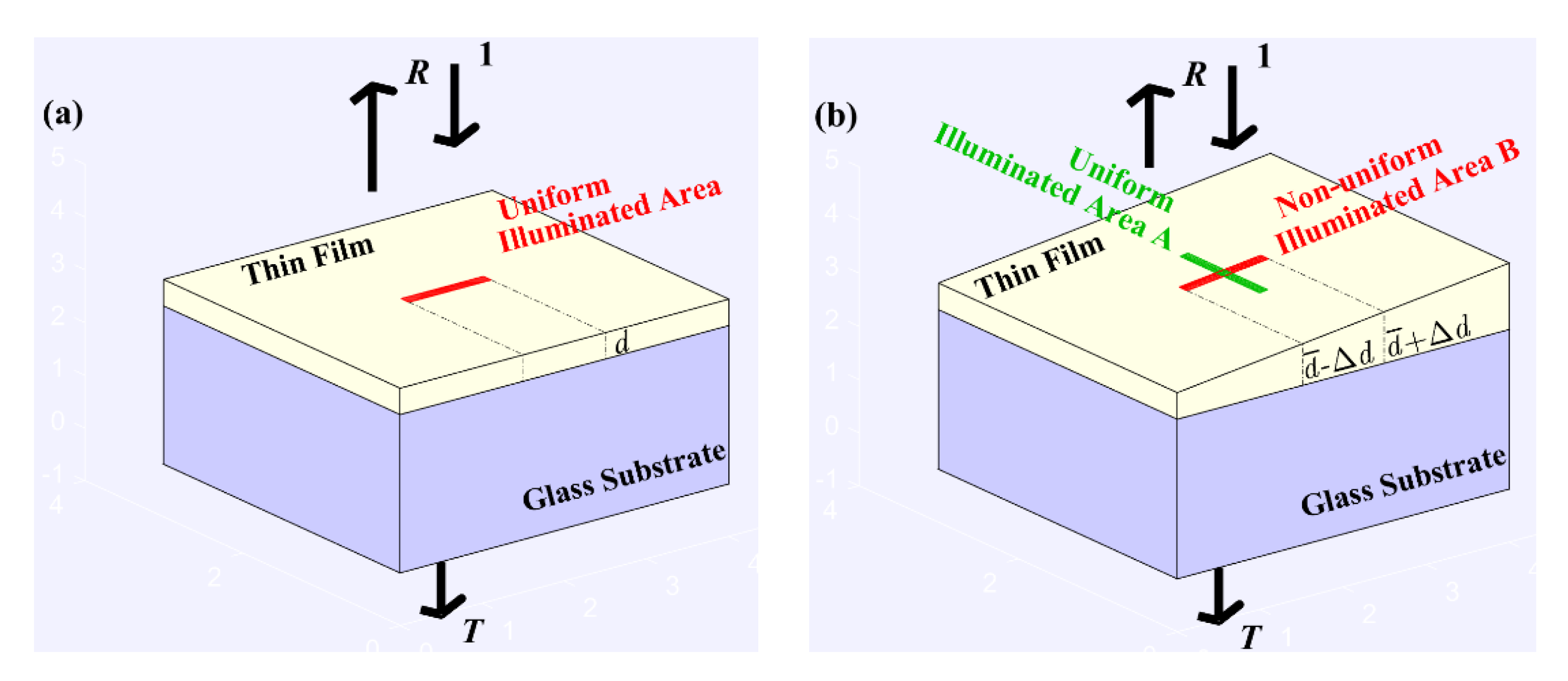
3.2. Effect of Non-Uniformity of the Thin-Film Thickness on the Transmission Spectrum

By definition, the thickness of an idealized homogenous film is obviously constant, but in real samples it is rarely the case, and non-uniformity in thickness or surface roughness are commonly present in real films. The simplest way to model the geometry of a non-uniform film is to assume such a film having a wedge shape, as displayed in Figure 1b. Therefore, the thickness of the as-deposited film has a linear dependence upon the position in the sample, along the area illuminated. In order to quantify this thickness variation, a wedging parameter, Δ d , is defined and also an average thickness, d ¯ , so that the actual thickness varies linearly from d   = d ¯     Δ d up to d   = d ¯   +   Δ d .
It will be shown in detail below that a small variation in thickness over the area illuminated by the spectrophotometer has a significant effect on the interference pattern of the transmission spectrum. Non-uniformity in film thickness destroys the coherence of the light beams inside the film, and hence shrinks the transmission spectrum. Figure 2 clearly displays the effect of the non-uniformity of thickness on the transmission spectra for four simulated films of a - Si : H , with different values of Δ d , having postulated the following optical and geometrical parameters [26,31]:
λ   =   500 900 nm n   =   2.6   +   3   ×   10 5 λ 2 k   =   λ 4 π 10 ( 1.5   ×   10 6 / λ 2 ) 8   s   =   1.51 ( constant )   d ¯ = 1500   nm Δ d   =   0 , 10 , 20 , 30 , 60 nm  
In order to generate the spectral transmittance of a uniform layer ( Δ d   =   0 ) , Equation (6) has been used, whereas for the other four model-generated transmission spectra with four values of the wedging parameters ( Δ d   =   10 ,   20 ,   30 ,   60 ) , all depicted in Figure 2, the numerical integration of Equation (10) has been instead performed. These latter four shrunk generated spectra tend to the interference-free curve, T α (this curve will be discussed later), as Δ d increases.
The clear influence of a relatively high value of Δ d on the transmission spectrum is displayed in Figure 2. For the value of Δ d   =   60   nm , approximately at λ   =   750 nm , there is a particular point from which, for wavelengths λ     750 nm , a phase difference is noticeable with the other generated spectra, with a pre-established value of Δ d smaller than 60 nm, this phase difference being close to π radians, roughly speaking. This influence shall be dealt with in detail later.
It should be emphasized that if the effect of the non-uniformity in thickness on the transmission spectrum is neglected, and the layer is erroneously assumed to have a constant thickness throughout the beam-light spot, then the results obtained in the characterization of this non-uniform sample ignoring this effect, would lead to inaccurate information about the specimen, in particular: (i) an overestimation of the absorption coefficient; (ii) an underestimation of the refractive index; and (iii) an overestimation of the film thickness.
Under the assumption of linear dependence of the film thickness, a more accurate expression for the transmittance, accounting for this variable thickness, could be derived by integrating on the two variables which depend upon the variable thickness, namely, the phase φ and absorbance x, already defined by Equation (5). However, the effect of the variable thickness on the absorbance is negligible compared with the much stronger effect on the phase. Under this simplifying assumption, the integral for the transmission is then expressed as follows:
T Δ d ( n , k , s , d ¯ , Δ d ; λ ) = 1 φ 2 φ 1 1 x 2 x 1 φ 1 φ 2 x 1 x 2 A 2 x B 2 C 21 x   cos ( φ )   +   C 22 x   sin ( φ )   +   D 2 x 2   d φ dx     1 φ 2 φ 1 φ 1 φ 2 A 2 x B 2 C 21 x   cos ( φ )   +   C 22 x   sin ( φ )   +   D 2 x 2 d φ
where
d ¯ Δ d     d   d ¯ +   Δ d
and
φ 1   =   4 π n ( d ¯   Δ d ) / λ φ 2   =   4 π n ( d ¯ +   Δ d ) / λ
It has to be stressed that the analytical integration of Equation (6) involves inverse hyperbolic functions: it is a complex formula obtained in this work for the first time, to the best of our knowledge, by using the Mathematica® software package (verison 10.0), and it is presented next after performing some algebraically manipulations [32,33],
T Δ d ( n , k , s , d ¯ , Δ d ; λ ) = 2 A 2 x K 3 ( φ 2 φ 1 ) ( tan h 1 ( K 1 / K 3 ) tan h 1 ( K 2 / K 3 ) )
with
K 1   =   ( C 22 x   +   ( B 2 x ( C 21   +   D 2 x ) ) tan ( φ 1 / 2 ) ) K 2     =   ( C 22 x   +   ( B 2 x ( C 21   +   D 2 x ) ) tan ( φ 2 / 2 ) ) K 3   =   ( B 2 2 2 B 2 D 2 x 2   +   x 2 ( C 21 2   +   C 22 2 D 2 2 x 2 ) )
For reasons that will become clear later, it is useful to express the transmission for a film-on-substrate specimen, using circular or goniometric functions instead of hyperbolic functions. After some manipulations, a convenient equation for the transmission is finally derived:
T Δ d ( n , k , s , d ¯ , Δ d ; λ ) = 2 A 2 x K 3 ( φ 2 φ 1 ) ( ( tan 1 ( K 1 / K 3 ) ) + ( tan 1 ( K 2 / K 3 ) ) )
It is stressed now that either Equation (15), or a simpler one obtained by integrating Equation (3) instead of Equation (6) [26,31], cannot be employed in the characterization of semiconductor films. The presence of a multi-valued inverse circular function in Equation (15), is responsible for the discontinuities around the minima (if the appropriate angles, multiples of π, are not taken into account). It should be pointed out that the existence of such discontinuities makes Equation (15) useless. This is demonstrated in Figure 3a, where such an equation is plotted in the case of a postulated a - Si : H film, whose wedging parameter has a value of 30 nm. It is seen in Figure 3a that this transmission curve matches the numerical integration of Equation (10) except around the minima of transmission. Lastly, Equation (15) will be used later to derive the expression for the upper envelope of the transmission curve.

3.3. Effect of the Optical Phase Variation within the Semiconductor Thin Layer

The terms K1 and K2 in Equation (14) contain an angle or goniometric function, whose corresponding arguments φ 1 and φ 2 are given by Equation (12). Depending on the particular values of n, d ¯ , Δ d , and λ , the argument of the angle or goniometric functions can exceed or not the limit of 2π radians. Taking into account that those two terms K1 and K2 are within inverse goniometric functions, it is therefore necessary to account for the number of multiples of 2π added to the optical phase. This key step does indeed eliminate the clearly invalidating discontinuities displayed in Figure 3a,b.
In order to correct for the effect of the thickness non-uniformity on the transmission spectrum of the layer, we have proposed [32] to add two integer numbers in the corresponding expression to account for the correct optical phase. Thus, the new corrected expression of the transmission is finally derived,
T Δ d ( n , k , s , d ¯ , Δ d ; λ ) = 2 A 2 x ( ( tan 1 ( K 1 / K 3 ) + N 1 π ) + ( tan 1 ( K 2 / K 3 ) + N 2 π ) ) K 3 ( φ 2 φ 1 )
where the two correcting integer numbers,   N 1 and   N 2 , respectively, are given by:
N 1   =   round   ( φ 1 / 2 π ) N 2   =   round   ( φ 2 / 2 π )
The function ‘round’ rounds off the argument to its closest integer number, and corresponds to the function with the same name implemented in the mathematical software package MATLAB® (Version: R2019A) used later. The new Equation (16) derived in this work is a continuous function that can be employed to characterize a great variety of amorphous semiconductors.
The physical relevance of Equation (16) is twofold: (i) the transmission spectra of non-uniform layers can be characterized by using inverse-synthesis methods [34], rather than those methods based only on the top and bottom envelopes of the transmission spectrum; and equally important, (ii) the exclusion of non-uniform films having a large wedging parameter [26,31,34,35], is eliminated, as will be shown below with both simulated and measured spectra, which so far would have been considered useless.

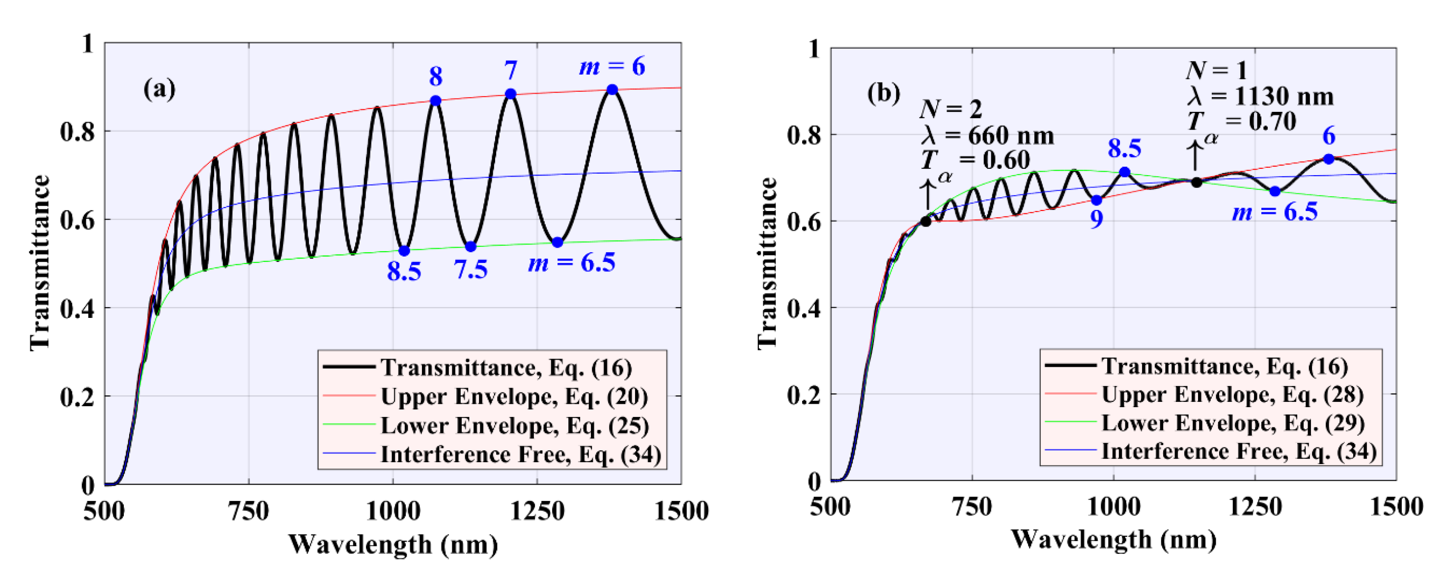
3.4. Derivation of an Expression for the Upper Envelope of the Transmission Spectrum

The derivation of a novel expression for the upper envelope of the transmission T Δ d   Max is now straightforward, but only when the value of Δ d is smaller than a certain limiting value. The equation for the existence of Fabry–Perot interference fringes, to be obeyed by the maxima and minima of such a pattern (see Figure 3), is as follows,
2 n d ¯ = m λ
The order number, m, is an integer number for the maxima, and half-integer for the minima.
In Equation (15), the oscillating behavior of the transmission is caused by the trigonometric functions tan   ( φ 1 / 2 ) and tan   ( φ 2 / 2 ) into the two terms K1 and K2, respectively, with the corresponding two phase angles φ 1 and φ 2 given by Equation (12). So, by using some trigonometric identities and introducing Equation (18) into Equation (12), it is found that for the maxima, where m = 1, 2, 3,…, and therefore tan   ( m π )   =   0 , it follows,
tan ( φ 1 / 2 ) = tan ( 2 π n ( d ¯ Δ d ) / λ ) =   tan ( 2 π n Δ d / λ ) tan ( φ 2 / 2 ) = tan ( 2 π n ( d ¯ + Δ d ) / λ ) =   + tan ( 2 π n Δ d / λ )
Next, by introducing Equation (19) into K1 and K2 defined in Equation (14), we derive the expression for the upper envelope of the transmission spectrum:
T Δ d Max ( n , k , s , d ¯ , Δ d ; λ ) = 2 A 2 x K 3 φ 3 ( tan 1 ( K 4 / K 3 ) )
where K4 and φ3 are given, respectively, by:
K 4   =   ( C 22 x   +   ( B 2 x ( C 21   +   D 2 x ) ) tan ( φ 3 / 2 ) )
and
φ 3   =   4 π n Δ d / λ
Figure 3a shows that when Δ d is smaller than a limiting value, the expression for the upper envelope, Equation (20) (in blue), is correctly tangent to all the maxima of the spectrum. However, when the value of Δ d is larger than the just-mentioned limiting value, the same equation becomes not useful in order to determine the optical constants of the film, as displayed in Figure 3b.

3.5. Derivation of an Expression for the Lower Envelope of the Transmission Spectrum

The derivation of the expression for the lower envelope of the transmission spectrum,   T Δ d Min , is more complex, regardless the value of Δ d . As shown in Figure 3a,b, Equation (15) shows discontinuities in both cases considered. For these minima, again applying the basic equation for interference fringes, but with the different values of m = 0.5, 1.5, 2.5, 3.5,…, and hence tan   ( m π )   =   ± , it is verified that
tan ( φ 1 / 2 ) = tan ( 2 π n ( d ¯ Δ d ) / λ ) =   + cot ( 2 π n Δ d / λ ) tan ( φ 2 / 2 ) = tan ( 2 π n ( d ¯ + Δ d ) / λ ) =   cot ( 2 π n Δ d / λ )
However, by introducing Equation (23) into Equation (14) does not lead to any useful function, since we would obtain the expression for the lower envelope plotted in green in Figure 3a,b, which is clearly useless.
Therefore, in order find the lower envelope of the transmission spectrum we need to introduce now an auxiliary function Tπ, which consists of Equation (6), but adding this time a phase shift of π radians. Both functions have the respective maxima and minima exchanged each other, although both functions possess the same two envelopes.
T π   ( n , k , s , d ; λ )   =   A 2 x B 2   C 21 x   cos ( φ   +   π )   +   C 22 x   sin ( φ   +   π )   +   D 2 x 2 = A 2 x B 2   +   C 21 x   cos ( φ ) C 22 x   sin ( φ )   +   D 2 x 2
We could next follow the same steps followed in order to derive Equation (20) starting from Equation (6). However, a more straightforward approach is used, by taking into account that the difference between Equations (6) and (24) is only the opposite signs of the two coefficients C 21 and C 22 . Thus, the expression for the lower envelope of the transmission spectrum is derived, by changing the respective signs of C 21 and C 22 in Equations (20) and (21):
T Δ d Min ( n , k , s , d ¯ , Δ d ; λ ) = 2 A 2 x K 3 φ 3 ( tan 1 ( K 5 / K 3 ) )
where
K 5   =   ( C 22 x   +   ( B 2 x ( C 21   +   D 2 x ) ) tan   ( φ 3 / 2 ) )
As a summary, Equations (16), (20), and (25), are new expressions for the transmission and its top and bottom envelopes. However, whereas equation (16) is valid for any value of Δ d , both Equations (20) and (25), in their current form, are only correct for limited values of Δ d . As depicted in Figure 3a,b, corresponding to the generalized case of any non-uniform semiconductor film. Needless to say these three new Equations (16), (20), and (25), can be also successfully applied to uniform samples by only letting Δ d approach to zero.

4. Particular Case of a Film with Strong Thickness Non-Uniformity: Appearance of the Envelope-Crossover Points

In the literature, so far, all the available equations used in order to optically characterize non-uniform semiconductor films have the limitation of a range of allowed value of the wedging parameter, as mentioned before. When Δ d is larger than the maximum limiting value, the existing equations for the top and bottom envelopes of the transmission spectrum are discontinuous, and thus this spectrum is not usable. The range of validity of these already-reported equations for the two envelopes, Equations (20) and (25), respectively, is given by following inequality:
0   <   Δ d   <   λ / 4 n
In our analysis, it has been found that when this maximum limit for Δ d is reached, the transmission spectrum and its upper and lower envelopes are coincident. Moreover, when the value of Δ d is greater than such a maximum limit, then the lower envelope becomes greater than the upper envelope, and the equations for the top and bottom envelopes are discontinuous, as seen in Figure 3b. It should also be noted that at the particular wavelength λ   =   4 n Δ d , Equations (16), (20), and (25) merge to a single critical point with transmission Tα, and hence the optical interference pattern is totally destroyed.
From Figure 1b, it can be seen that this physically means an optical-path difference of λ / 2 between the thinnest and thickest parts of the light-spot area of the sample, and bears a clear similarity to the quarter-wavelength layers used for antireflection coatings. At this point the transmission is the interference-free or incoherent transmission, Tα [26]. For smaller values of λ , that is, for λ   <   4 n Δ d , a second interference pattern, starts to appear. We will call from now on this condition of binding or crossing envelopes, the envelope crossover [26,31,35,36], and the specific wavelengths at which these envelope-crossover points do occur, crossover wavelengths, or λ cross .
The equations of the top and bottom envelopes, Equations (20) and (25), respectively, are similar in structure to the expression for the transmission curve, Equation (16). Following exactly the same approach used above [32], we can again introduce a correcting factor to account for the multiples of 2π (consequence of the existing inverse goniometric functions), so that we can finally obtain absolutely usable equations for the upper and lower envelopes, which will allow the highly accurate characterization of a real non-uniform semiconductor film, very importantly, with a non-limited value of Δ d     λ / ( 4 n ) .
The expressions for the upper and lower envelopes of the transmission spectrum then become:
T Δ d Max ( n , k , s , d ¯ , Δ d ; λ ) = 2 A 2 x K 3 φ 3 ( tan 1 ( K 4 / K 3 ) + N 3 π )
T Δ d Min ( n , k , s , d ¯ , Δ d ; λ ) = 2 A 2 x K 3 φ 3 ( tan 1 ( K 5 / K 3 ) + N 3 π )
where the new correcting factor introduced is given by:
N 3   =   round   ( φ 3 / 2 π )
φ 3   =   4 π n Δ d / λ
and Non-uniform specimens having high values of Δ d can exhibit more than one envelope-crossover points in their strongly-shrunk spectra. The successive wavelengths associated to these envelope-crossover points obey the following equation:
λ cross   =   4 n Δ d / N ,   N   =   1 , 2 , 3 ,  
As has been pointed out, the result of increasing the wedging parameter on the transmission spectrum is making progressively converge such transmission spectrum towards the interference-free transmission curve Tα. Therefore, its expression is derived by integrating Equation (10) on the phase, φ, between a maximum and an adjacent minimum [25]:
T α ( n , k , s , d ¯ ; λ ) 1 π 0 π A 2 x B 2 C 21 x cos ( φ ) + C 22 x sin ( φ ) + D 2 x 2 d φ
This leads to a new expression for the interference-free transmission curve, Tα,
T α ( n , k , s , d ¯ ; λ ) = A 2 x K 3
In Figure 4a,b, we have plotted the novel equations of the transmission, its top and bottom envelopes, and the interference-free transmission, for the postulated a - Si : H film, with a small value for Δ d of 30 nm, and also a large value of 100 nm. The four transmission curves plotted merge at those existing two crossover points (see Figure 4b).
The physical significance of the expression for T α , Equation (34), which does not contain any trigonometric function, should be emphasized. In the transparent region k = 0 and x = 1 and, therefore, if an envelope-crossover point is found in the as-measured spectrum, then Equation (34) can be solved for n. In addition, since at the envelope-crossover points Equation (32) is obeyed, we can then calculate an alternate value for Δ d by using a dispersion-model-free approach, which can be compared with that obtained from the present inverse synthesis method. In Figure 4b, on the other hand, two envelope-crossover points are seen, corresponding to N = 1 and N = 2, Equation (32). Their particular values for the transmission and wavelength, together with their values for n and Δ d , are shown in Table 1. The bigger difference with the postulated value of the wedging parameter of 100 nm is larger in the case of λ cross   =   660 nm (see Table 1), due to the fact of a higher value of the extinction/absorption coefficient for this smaller crossover wavelength.

5. Optical Properties of Amorphous Semiconductor Films: Using the Tauc–Lorentz–Urbach Parameterization

The glass substrate on which the film is deposited is confirmed to be transparent in the whole spectral range under study, and hence completely characterized by its real refractive index S. This optical parameter was determined from independent transmission measurements on the bare glass substrate, by using the well-known equation for the transmission of a non-absorbing layer, TS:
T s ( s ;   λ )   =   2 s s 2   +   1
The amorphous semiconductor film, on the other hand, will be optically and geometrically characterized by its complex refractive index n, along with the average thickness d ¯ and wedging parameter Δ d . In addition, the Kramers–Krönig-consistent optical dispersion model that is employed in this work for the investigated films, is the Tauc–Lorentz–Urbach (TLU) model or parameterization, as proposed by Foldyna [37]. This TLU model is appropriate for amorphous semiconductors and dielectrics, and is a generalization of the Tauc–Lorentz parameterization suggested by Jellison and Modine [38,39], with the exponential Urbach tail added. This TLU parameterization includes six free fitting parameters: A, E0, C, Eg, Ec, and ε 1 , .
In the TLU model, the imaginary part of the complex dielectric function ε 2   ( E ) is expressed as follows:
ε 2 ( E )   =   { 1 E A E 0 C ( E E g ) 2 ( E 2 E 0 2 ) 2   +   C 2 E 2 ,   E     E c A u E exp ( E E u ) ,   0   <   E   <   E c
where the first term of ε 2 ( E ) for E     E c is identical to the Tauc–Lorentz parameterization, and the second term for 0 <   E   <   E c expresses the Urbach tail. The free fitting parameters Eg, A, E0, and C denote the bandgap energy, oscillator, amplitude, Lorentz resonant energy, and broadening parameter, respectively.
Moreover, the constants A u and E u , the so-called Urbach amplitude and energy, respectively, have been introduced to ensure the continuity of the previous function, and also its first derivative:
E u   =   ( E c E g ) [ 2 2 E c ( E c E g ) C 2   +   2 ( E C 2 E 0 2 ) C 2 E C 2   +   2 ( E C 2 E 0 2 ) 2 ] 1 A u   =   exp ( E c E u ) A E 0 C ( E c E g ) 2 ( E C 2 E 0 2 ) 2   +   C 2 E C 2
The real part of the complex dielectric function,   ε 1 ( E ) , is obtained by using the analytical integration corresponding to the Kramers–Krönig relationship between ε 1 ( E ) and ε 2 ( E ) :
ε 1 ( E )   =   ε 1 ,   +   2 π ( C . P . ) 0 ξ ε 2 ( E ) ξ 2 E 2 d ξ
where ‘C.P.’ stands for the Cauchy Principal value of the integral. This leads to:
ε 1 ( E )   =   ε 1 ,   +   ε 1 , TL ( E )   +   ε 1 , UT ( E )
where the Tauc–Lorentz part from E c     E   <   is expressed by:
ε 1 , T L ( E ) = A E 0 C E 2 + E g 2 π ς 4 E ln ( | E c E | E c + E ) + 2 A E 0 C E g π ς 4 ln ( | E c E | ( E c + E ) ( E 0 2 E c 2 ) 2 + C 2 E c 2 ) + A C a L 2 π ς 4 α E 0 ln ( E 0 2 + E c 2 + α E c E 0 2 + E c 2 α E c ) A a A π ς 4 E 0 [ π tan 1 ( 2 E c + α C ) tan 1 ( 2 E c α C ) ] + 4 A E 0 E g E 2 γ 2 π ς 4 α [ π 2 tan 1 ( 2 ( E c 2 γ 2 ) α C ) ]
and where the intermediate variables used are given here for the sake of completeness, by the following expressions:
a L   =   ( E g 2 E 0 2 ) E 2   +   E g 2 C 2 E 0 2 ( E 0 2   +   3 E g 2 ) a A   =   ( E 2 E 0 2 ) ( E 0 2   +   E g 2 )   +   E g 2 C 2 γ   =   E 0 2 C 2 2 α   =   4 E 0 2 C 2 ς 4   =   ( E 2   E 0 2 ) 2 +   C 2 E 2
Furthermore, the Urbach-tail part for 0   <   E   <   E c is expressed by:
ε 1 , UT ( E )   =   A u π E exp ( E E u ) [ re ( expint ( E E u ) )   + re ( expint ( E c   +   E E u ) ) ]   + A u π E exp ( E E u ) [ re ( expint ( E c E E u ) ) re ( expint ( E E u ) ) ]
where the function ‘expint’ is the exponential integral function, as also implemented in MATLAB
expint   ( y )   =   y exp ( t ) t dt
and ‘re’ is the real component of y, since for negative values of y the corresponding integral result has an imaginary component that must be neglected.

6. Practical Application to Real Amorphous As-Based Chalcogenide Materials

The mathematical expressions already derived will now be employed in the characterization of some real chalcogenide layers. All the details of the procedure used in this work in order to accurately determine the optical properties of the non-crystalline chalcogenides under investigation follow below.

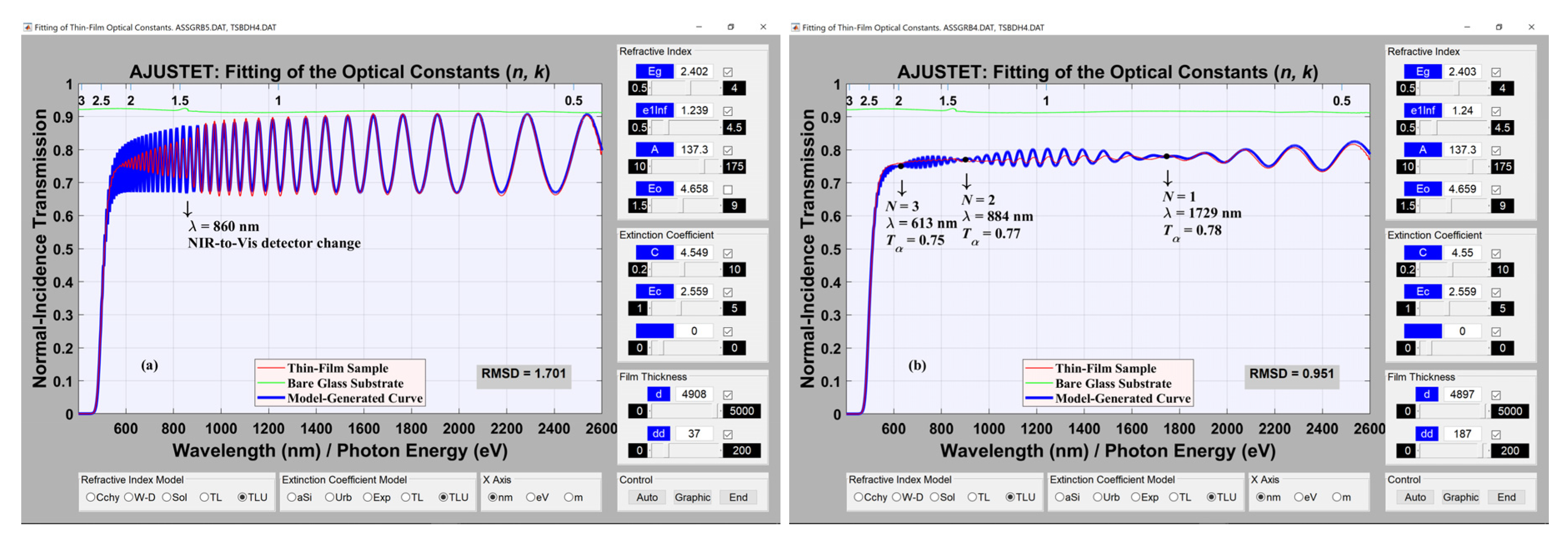
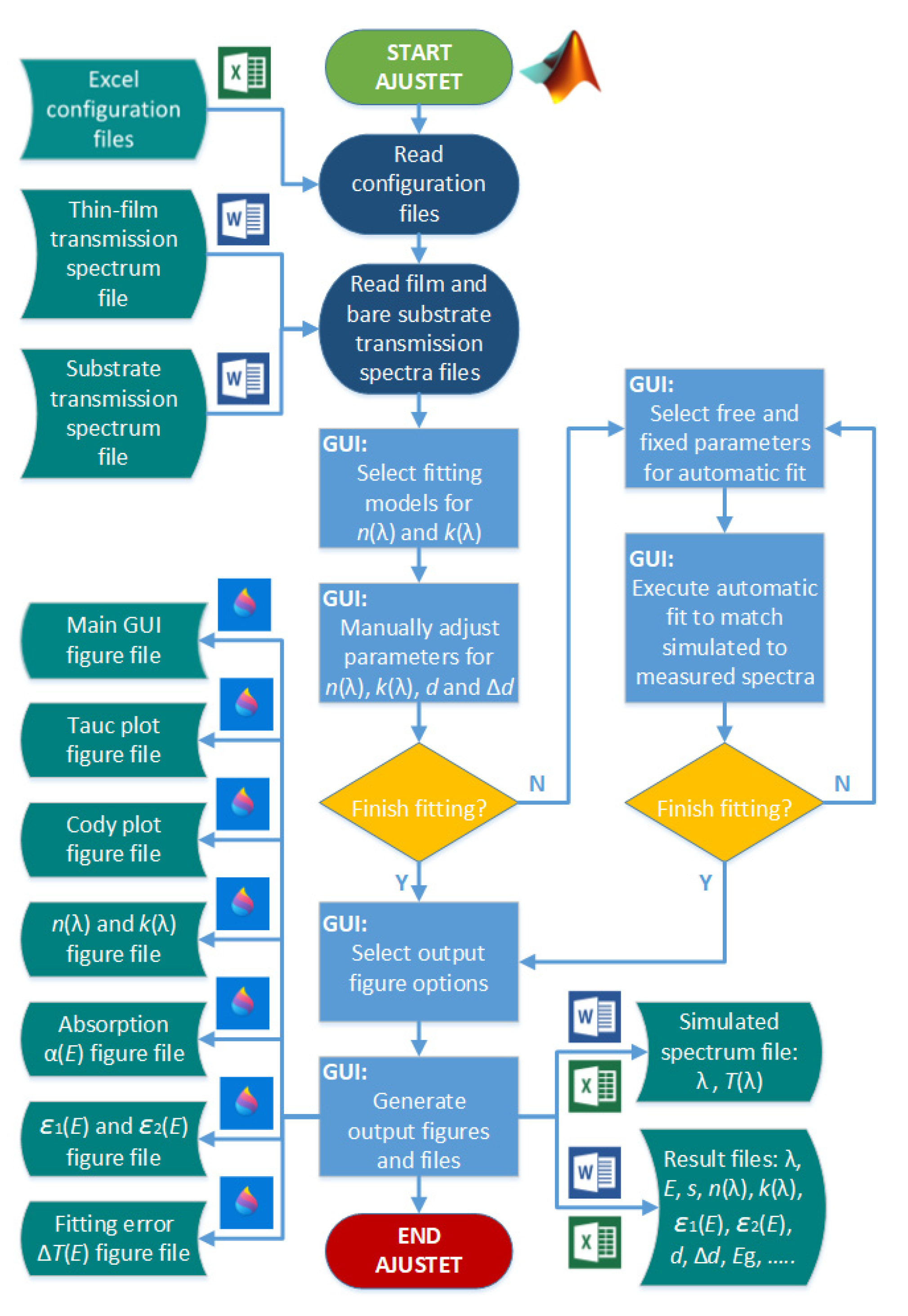
6.1. AJUSTET: Computer Program for the Optical Characterization of Semiconductor Films Based on Inverse Synthesis

The method devised in order to carry out the characterization of semiconductor films has been coded in MATLAB, and falls into the category of inverse-synthesis methods [34]. The software developed can accurately fit a model-generated transmission spectrum to the experimentally-measured spectrum of a semiconductor film, by adjusting up to a maximum of nine free fitting parameters: (i) seven associated to the optical dispersion relationships, plus (ii) two non-uniform-sample geometrical parameters, the average thickness and the wedging parameter, d ¯ and Δ d , respectively.
Up to five different optical-dispersion models for n ( λ ) , and another three for k ( λ ) , have been so far implemented in the MATLAB-coded application, AJUSTET. They include a purely-empirical model, as the Cauchy dispersion relationship, and two physics-based models as those proposed by Wemple-Domenico [40,41], the single-effective-oscillator fit, and Solomon [42], that corresponding to the band-structure determination, respectively, for n ( λ ) . In addition, the exponential and Urbach functional models for k ( λ ) [21]. Moreover, two coupled physics-based models that link n ( λ ) and k ( λ ) through the Kramers–Krönig relationships, as the popular Tauc–Lorentz [38,39], and the much less frequently-used Tauc–Lorentz–Urbach [37] dispersion models, have been also implemented in the developed computer program, AJUSTET.
Lastly, the main idea behind the computer program AJUSTET, in the present case for the determination of the TLU parameters, is to find their values which minimize the following figure-of-merit (FOM) or goodness-of-fit function:
FOM     RMSD   =   i   =   1 N ( T i , meas   T i , simu ) 2 N
where N is the number of data points measured, T i , meas is the as-measured optical transmittance, and T i , simu is the simulated optical transmittance, for vacuum wavelengths for which the glass substrate used is non-absorbing. The statistic function FOM to be minimized is therefore the root-mean-square deviation (RMSD) of the differences between the experimentally-measured and model-generated optical transmittance data; or, in other words, the square root of the average of squared optical transmittance differences. In AJUSTET, for the minimization routine, the Nelder and Mead (downhill) simplex algorithm in the MATLAB software was utilized; a non-linear direct search method, implemented in the MATLAB ‘fminsearch’ function, was employed in order to find the minimum of an unconstrained multivariable function.
Regarding the data output of AJUSTET (see the detailed flowchart of the complete algorithm of MATLAB-based software AJUSTET in the Appendix A), it should be pointed out that the program AJUSTET is fully configurable through external excel files. It requires as data inputs, the as-measured transmission spectra belonging to the chalcogenide sample, together with that of its bare glass substrate. Upon completion of the execution phase of the program AJUSTET, it provides the following outputs: (i) the Tauc [43] and Cody [44] plots (that is, the so-called Tauc and Cody extrapolations), respectively, where the Tauc and Cody gaps, Eg, Tauc and Eg, Cody, respectively, along with the Tauc and Cody slopes, βTauc and βCody, respectively, are determined; (ii) the optical-absorption edge, where the three iso-absorption gaps, E03, E04 and E05, associated to the values of α of 103, 104, and 105 cm−1, respectively, are indicated; (iii) two figures plotting both the real and imaginary parts of the complex refractive index, n, and those of the complex dielectric function, ε, as a function of the vacuum wavelength or photon energy; (iv) another figure plotting the differences between the generated and as-measured transmission spectra; and (v) a final figure plotting the generated spectrum, together with its two calculated top and bottom envelopes. All these figures can be conveniently exported to individual files.

6.2. Case Study of Thermally-Evaporated Reasonably-Uniform and Non-Uniform Amorphous Chalcogenide Films

6.2.1. Chalcogenide Sample Preparation Procedure and Optical Transmittance Measurements

The amorphous As-based chalcogenide material prepared for our case study corresponds to the binary chemical composition As33S67. This has been deposited by conventional thermal evaporation of the bulk glass onto room-temperature, 1-mm-thick BDH glass substrates, inside a vacuum chamber with a base pressure of around 10−7 Torr. The evaporation system was equipped with a rotatory accessory device in order to make it possible the deposition of films with a reasonable degree of thickness uniformity, if wished [27,28]. The non-crystalline nature of the material was confirmed by both X-ray diffraction measurements and Raman spectroscopy. Besides, the chemical composition was carefully checked out by energy dispersive X-ray spectroscopy, and was determined to be 32.9 ± 0.4 at.% As and 67.1 ± 0.6 at.% S, which is particularly close to the nominal chemical composition AsS2 (i.e., As33S67).
For this case study, specific positions of the chalcogenide samples inside the vacuum chamber were selected, in order to be able to both deposit reasonably uniform, as well as slightly-wedge-shaped samples, with thicknesses in the particular range 1000 nm < d ¯ < 2000 nm. Such specimens were used to study the influence of the ‘wedgeness’ on the transmission spectra, and also the performance of the proposed equations for the transmission of a uniform and non-uniform film on a transparent substrate, Equations (6) and (16), respectively.
Furthermore, in order to be able to perform the characterizations of chalcogenide layers with very high values of the wedging parameter, films were also grown with larger thicknesses, such that d ¯ < 5000 nm, and much higher wedging parameter, such that Δ d ≤ 200 nm, in order to investigate in real samples the appearance of envelope-crossover points in the interference pattern, as predicted by the theory outlined above.
The experimental normal-incidence transmission spectra of the chalcogenide samples under study, on the other hand, were measured by a Lambda 1050 Perkin-Elmer UV/Vis/NIR double-beam spectrophotometer (Perkin-Elmer Corporation, Waltham, MA, USA). The measured wavelength range was 400 nm     λ     2200 / 2600 nm . The room-temperature transmission measurements were made at wavelength steps of either 1 nm or 0.6 nm, depending upon the particular characteristics of each layer; specifically, the smaller wavelength step of 0.6 nm was employed in the thicker layers, in order to be able to resolve in a better way the very large number of data oscillations, particularly at the smaller visible wavelengths analyzed. Furthermore, a feature appears in the spectra for transmittance in the case of the thicker samples explored with the 0.6-nm step, in the spectral region of 860 to 900 nm. It can be more clearly seen (Figure 5) on the transmission spectrum of the bare glass substrate, in the just-mentioned wavelength range. This noticeable artefact results from the change of detectors in the UV/Vis/NIR spectrophotometer employed, at the default value of wavelength of 860 nm. As an additional characteristic feature of the amorphous chalcogenides studied, to the unaided eyes the as-deposited layers appear pale yellow. A photo of an amorphous arsenic sulfide layer deposited by thermal evaporation, taken by a digital camera, is shown in the inset of Figure 5b.
Two representative chalcogenide samples, and their corresponding four spectra (two for each sample), were studied in order to carry out their optical characterizations. Each sample was illuminated at two cross orientations in the same location, as seen in Figure 1b. The illuminated area A was selected in such an orientation of the sample, as to be able to find the best thickness uniformity possible along the light spot. The illuminated area B, on the contrary, was chosen in a direction perpendicular to the previous one, as to find the direction with the largest thickness gradient, instead. These cross-illuminated areas have allowed us the comparison of the experimental results of two independent characterizations, which have shown an excellent agreement indeed between the calculated optical properties and average thicknesses, obtained from the pair of normal-incidence transmission spectra.
The four aforementioned transmission spectra and that of the bare-substrate spectrum are depicted in Figure 5. The spectra S1 and S2 belong to the thinner (approximately 1600-nm-thick) film, whereas the spectra S3 and S4 correspond to the thicker (approximately 4900-nm-thick) film. It is worth mentioning the strong influence on the spectra caused by the existence of a clear wedge shaping, especially notable when comparing the spectra S3 and S4 belonging to the much thicker sample. It has to be also pointed out the strong influence on the spectrum S3 in the visible-to-NIR region, with a large shrinkage of the interference pattern caused by the integration performed by the spectrophotometer, since this cannot precisely follow the numerous fringes of the very thick layers, due to its inherent limitation of a non-zero spectral bandwidth.

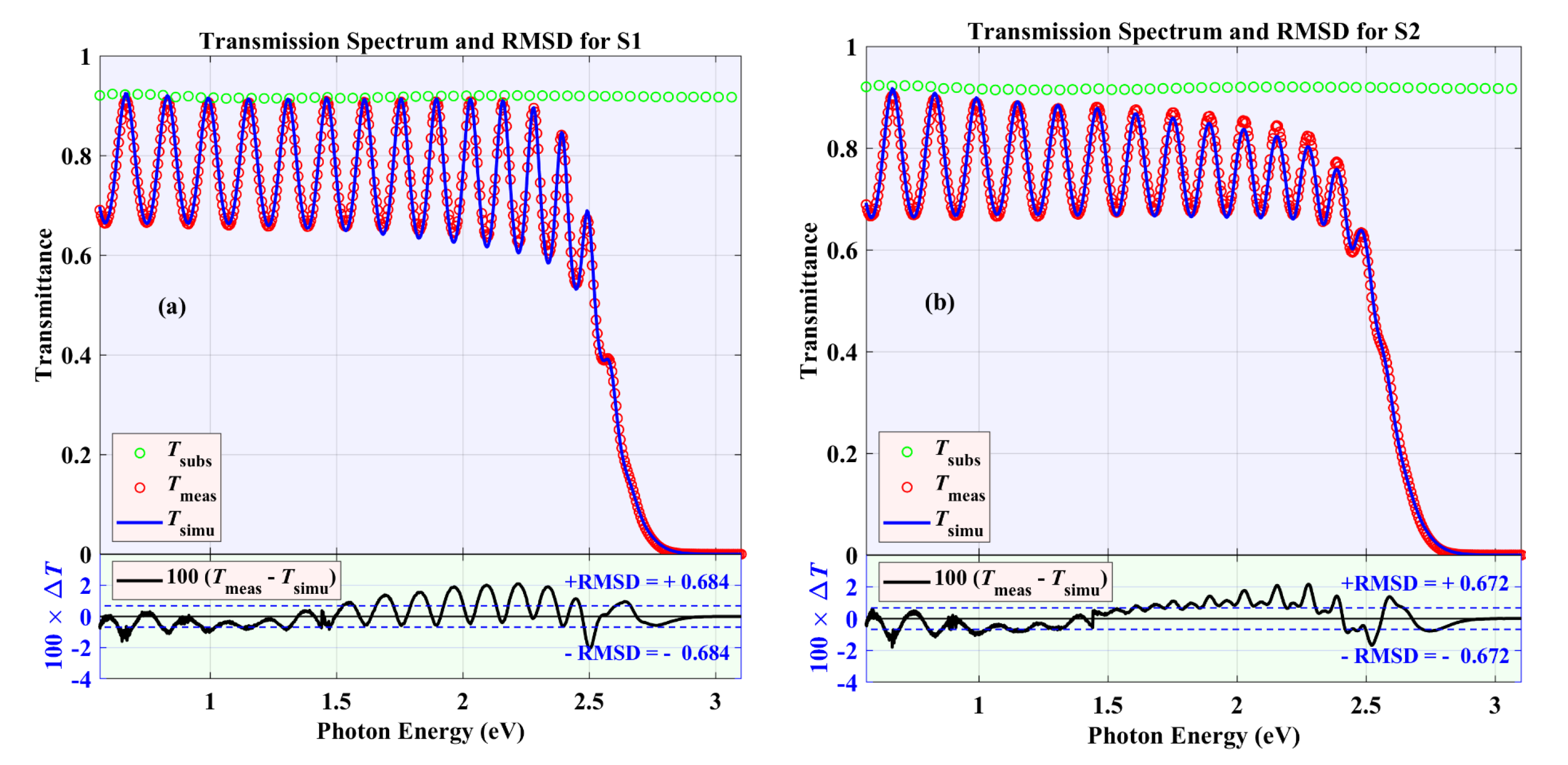
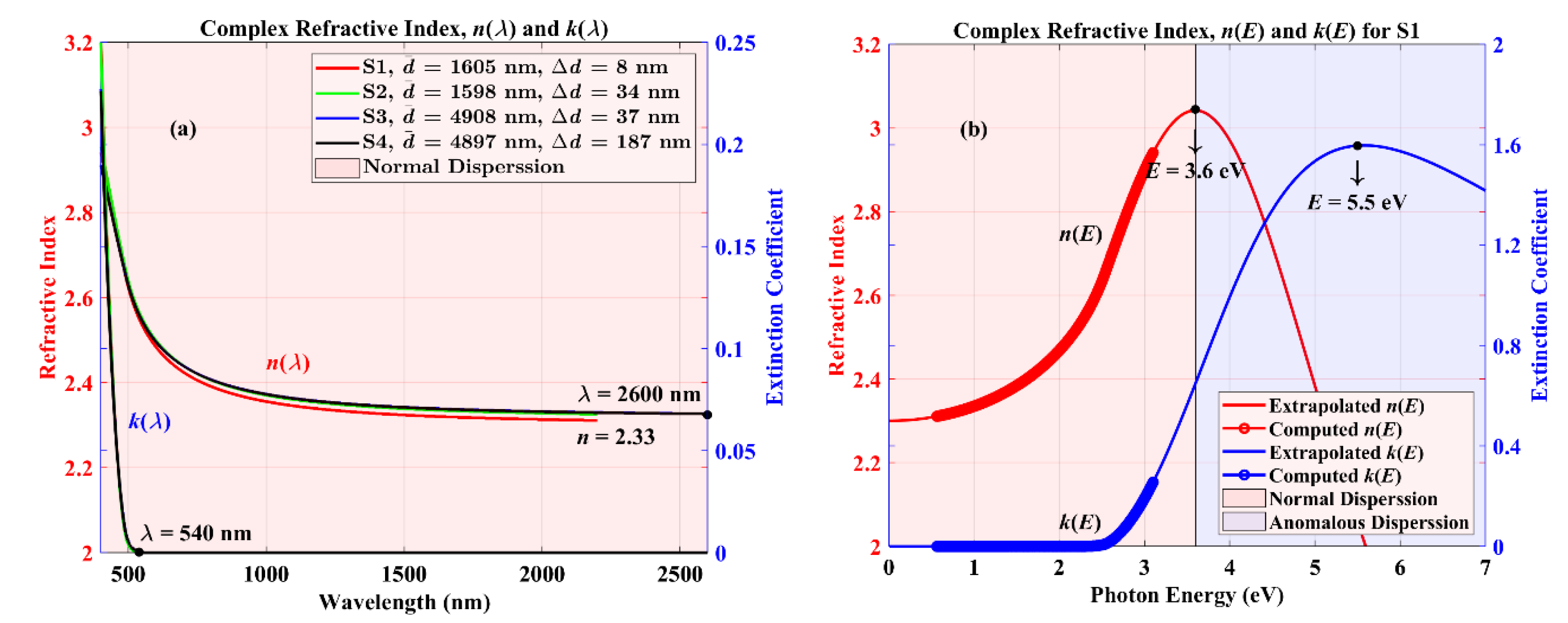
6.2.2. Experimental Results Obtained Using AJUSTET

The four transmission spectra S1 to S4 displayed in Figure 5 were independently analyzed by the computer program AJUSTET, and in Table 2 all the best-fit parameters corresponding to the TLU model employed, for each of the four representative transmission spectra, are listed. Furthermore, Figure 6a,b, show the comparison between the model-generated and as-measured transmission spectra for the cases of the spectra S1 and S2. The difference between the simulated and experimental spectra, ∆T, for those spectra S1 and S2 is also displayed in this figure.
It is noticed the extremely good agreement between the as-measured and generated transmission spectra, with very low values of RMSD of 0.684 and 0.672, respectively. For the sake of clarity, the x-axis represents photon energy when plotting the spectral transmittance, and we have also used open circles instead of solid lines, in order to plot the experimental transmission data for this thinner chalcogenide sample.
On the other hand, the carefully-designed GUI (main window) of the software application AJUSTET, displaying the values of all the free-fitting parameters involved in the optical and geometrical characterizations corresponding to of the transmission spectra S3 and S4, are shown in Figure 7a,b, respectively; the low obtained values of RMSD, 1.701 and 0.951, respectively, have indicated the very good correlation between the as-measured and calculated transmittance data, for these two particular transmission spectra corresponding to the thicker sample. In these two GUIs belonging to the much more complex and challenging spectra S3 and S4, the simulated and experimental solid transmittance curves are plotted, instead, as a function of vacuum wavelength, following the transmission data directly obtained from the double-beam spectrophotometer. These certainly very deformed spectra were also purposefully selected to test the actual capabilities of the UV/Vis/NIR spectrophotometer used in our investigation, as fully as possible.
There exist three clear envelope-crossover points appearing in the transmission spectra S4. Both optical spectra belonging to the almost-5 μm-thick sample, to the best of our knowledge, were not useful for their optical characterization, using the currently available formulae in the literature for the transmittance of a thin weakly-absorbing layer onto a thick transparent substrate. However, the use of the Equation (16) was indeed the key factor to be able to successfully analyze of the strongly-shrunk transmission spectra S4, otherwise absolutely useless.
The calculated complex refractive indices of the two chalcogenide samples under study, as a function of wavelength, are plotted in Figure 8a. On the other hand, the refractive index, n(E), and extinction coefficient, k(E), as a function of photon energy, instead, of a representative spectrum, are both displayed in Figure 8b. The average thickness of this particular slightly-wedge-shaped specimen was 1605 nm, and the corresponding very small wedging parameter was 8 nm: it clearly demonstrates the strong sensitivity of the devised characterization technique, based on the transmission spectrum only. It is seen in Figure 8b that n is initially an increasing function of the photon energy (i.e., d n ( E ) / d E   >   0 ). The optical dispersion is then said to be normal. For values of the photon energy larger than around 3.6 eV, the refractive index, on the contrary, decreases with increasing photon energy (i.e., d n ( E ) / d E   <   0 ), and we instead refer to the spectral region of anomalous optical dispersion. Because of the Kramers–Krönig relationships, the observed energy dependence of the refractive index is related to the existing chalcogenide-material absorption, described by its extinction coefficient, k (see Figure 8b). There is a very noticeable optical-absorption band around the value of photon energy of approximately 5.5 eV.
Best-fit TLU parameters for the two representative films (four selected transmission spectra) are listed in Table 2. For all cases, the amplitude of the TLU oscillator A is around 135 eV, and the bandgap value Eg is approximately 2.41 eV. The values of the parameters E0, C, EC and the offset, ε 1 , , are about 4.49 eV, 4.11 eV, 2.57 eV, and 1.37, respectively. It is noted at this point that, in the present physical interpretation of the experimental results, the concept of bandgap still survives even in the absence of crystallinity (long-range order) of the material, through the influence of the existing short-range ordering of the atomic structure in the non-crystalline chalcogenides, on their electronic density of states.
The value of the Urbach energy parameter, Eu, calculated from the just-mentioned TLU parameters, are also presented for each transmission spectrum in Table 2. The average thicknesses and wedging parameters corresponding to the four selected spectra are also listed in Table 2. Interestingly, the values of the Tauc and Cody gaps, Eg, Tauc and Eg, Cody, respectively (we will discuss them below), the three iso-absorption gaps, E03, E04 and E05, and the value of the refractive index at the specific photon energy of 1 eV (wavelength of 1240 nm), n(1 eV), all determined using the program AJUSTET, are also presented in Table 2. Last but not least, our TLU parameters are comparable and clearly consistent with those reported by the authors in a previous paper for the case of for spin-coated a-As33S67 films [29], and with the values of the Tauc–Lorentz parameters belonging to As40S60 (i.e., the As2S3 stoichiometric composition) bulk-glass material, reported by Jellison and Modine [38,39].

6.2.3. Alternative Independent Determination of the Tauc and Cody Optical Band Gaps

The absorption coefficient, α(E), was obtained, alternatively, directly from the transmission spectrum, exclusively in the region of strong absorption of the spectrum where the interference fringes absolutely disappear (see Figure 6). For very large values of α where the absorbance x   < <   1 , the interference effects can be ignored, and the transmission can then be written following Equation (8) as:
T meas     A 1 exp ( α d ¯ ) B 1 = 16 n 2 s exp ( α d ¯ ) ( n + 1 ) 3 ( n + s 2 )
and the absorption coefficient is obtained from:
α 1 d ¯ ln ( B 1 T meas A 1 ) = 1 d ¯ ln ( ( n + 1 ) 3 ( n + s 2 ) T meas 16 n 2 s )
Tmeas being the as-measured transmission, and the expressions of the parameters A2 and B2 being previously given by Equation (7).
Thus, we have finally reached an equation absolutely equivalently to Equation (22), from the seminal work by Swanepoel [25] on the optical characterization of thin films. He also proposed the use of the two-term Cauchy empirical relationship for the spectral dependence of the index of refraction, whereas we have more accurately used the expression for n(E) resulting from the Kramers–Krönig-consistent TLU dispersion model, considered in the present study.
Tauc et al. [43], on the other hand, have shown that for α > 104 cm−1 (Tauc´s region)
( α E ) 1 / 2   =   β Tauc ( E E g , Tauc )
This equation is a well-known formula very often employed in order to determine the Tauc optical gap Eg, Tauc from the just-calculated values of α(E) (Tauc´s extrapolation). In addition, Cody et al. [44] have derived the so-called Cody formula, given by
( α / E ) 1 / 2   =   β Cody ( E E g , Cody )
The slope βCody and ‘Cody gap’ Eg,Cody, both calculated by the Cody´s extrapolation, are not the same as those obtained from the Tauc model, Equation (47). Usually, it is verified that Eg,Cody < Eg,Tauc, and our results have confirmed that particular finding.
Continuing with the analysis of the experimental results, the α(E) data for the present chalcogenide layers were examined via both Tauc and Cody approximations. At least above certain (~2.65 eV) energy, and within some energy region (up to ~2.90 eV), both methods of analysis accurately fit the optical absorption data. Figure 9a,c display the fit to Equation (47), and Figure 9b,d exhibit the results of the Cody plot, Equation (48), for the same as-deposited (un-annealed) chalcogenide specimen.
It is also interesting to show the results of the Tauc´s extrapolation for the thicker chalcogenide layer. Its corresponding fitting energy range, as well as that for the thinner layer, are both highlighted in Figure 9. The much smaller fit region for the thicker sample (from 2.66 to 2.72 eV), is the direct consequence of its larger film thickness, more precisely, more than three times thicker. Something similar can be said about the Cody´s extrapolation for this much thicker chalcogenide film. In addition, it has been illustrated in Figure 9b,d both the exponential (low-energy) Urbach tail, starting from the values of E < E04, and the high-energy (absorption) spectral region, where the Tauc and Cody optical gaps were calculated; it has been found in our study that the iso-absorption gap E03 practically coincides with the Tauc gap, as it is generally considered.
In the present work, it has been finally reached the conclusion that the three spectral components of the TLU model, that is, the Lorentz electron oscillator, the Tauc joint density of states, and the Urbach exponential tail, respectively, very accurately describe both the below-band-gap and above-band-gap absorption in the As-based chalcogenide films under study. The ‘trade-off’ between the three spectral components has resulted in the small reduction of the nominal band gap Eg (TLU gap) relative to the true Tauc and Cody optical band gaps, Eg, Tauc and Eg, Cody, respectively, when the TLU-oscillator model has been fitted to the real transmission data; see Table 2, where all the calculated band-gap values are listed. We can conclude that part of the optical absorption of the material is embodied within the extra photon-energy range from the true extrapolated gap down to the fitted TLU gap. Thus, this TLU gap could be considered to certain extent a ‘mathematical gap’, rather than a purely-physical gap [45].

7. Concluding Remarks

The complex refractive index of thermally-evaporated amorphous As-based chalcogenide films deposited onto room-temperature glass substrates, was determined as a function of photon energy/wavelength with the aid of the devised MATLAB-coded computer program, AJUSTET, based only on the measurement of the normal-incidence transmission spectrum. The wavelength range studied was from 400 to 2200/2600 nm, and it has been unambiguously demonstrated that the TLU dispersion relation is certainly appropriate for the evaluation of the UV/Vis/NIR normal-incidence transmission measurements on amorphous chalcogenide layers.
Moreover, the average thickness values yielded by TLU evaluation are very close to the thickness values mechanically measured by a Dektak 150 surface profiler, and also by cross-section SEM microscopy images. The calculated complex refractive index spectra are in remarkable agreement with those reported by Jellison and Modine, confirming the correctness and accuracy of the new formulae for the optical transmittance, proposed in this paper. Besides, the values of the Urbach energy, Eu, deduced from the TLU parameterization, are also determined in the comprehensive optical characterization performed.
Finally, our computer program AJUSTET program has enabled us the accurate determination of the optical properties, average thickness and wedging parameter of films even thicker than up to approximately 5 μm, well above the preferred maximum thickness limit of the alternative, and, in general, much more difficult technique of variable-angle spectroscopic ellipsometry.

Author Contributions

J.J.R.-P.: conceptualization, investigation, writing—original draft preparation, software, validation, visualization. E.M.N.: conceptualization, investigation, writing—review and editing, validation, visualization, formal analysis, supervision. All authors have read and agreed to the published version of the manuscript.

Funding

This research received no external funding.

Acknowledgments

We sincerely thank Dorian Minkov (Technical University-Sofia, Bulgaria), Tivadar Lohner (Budapest University of Technology and Economics, Hungary), and Eduardo Blanco (University of Cádiz, Spain) for so many very useful discussions and comments during every phase of the present work.

Conflicts of Interest

The authors declare no conflict of interest.

Appendix A

The flowchart describing the user interaction with AJUSTET and the associated input and output files related to the software are depicted in Figure A1 below.
Figure A1. Flowchart for the algorithm corresponding to the MATLAB-based computer program AJUSTET, presented in the present work. It accurately resolves the problem of determining the optical constants, average layer thickness, and wedging parameter of amorphous semiconductor thin films.
Coatings 10 01063 g0a1

References

  1. Tanaka, K.; Shimakawa, K. Amorphous Chalcogenide Semiconductors and Related Materials, 1st ed.; Springer Science: New York, NY, USA, 2011. [Google Scholar] [CrossRef]
  2. Morigaki, K.; Kugler, S.; Shimakawa, K. Amorphous Semiconductors: Structural, Optical, and Electronic Properties, 1st ed.; John Wiley & Sons: Hoboken, NJ, USA, 2017; ISBN 978-1-118-75792-5. [Google Scholar]
  3. Atwood, G. Phase-change materials for electronic memories. Science 2008, 321, 210–211. [Google Scholar] [CrossRef]
  4. Cai, B.; Drabold, D.A.; Elliott, S.R. Structural fingerprints of electronic change in the phase change-material: Ge2Sb2Te5. Appl. Phys. Lett. 2010, 97, 191908. [Google Scholar] [CrossRef]
  5. Calvez, L.; Yang, Z.; Lucas, P. Composition dependence and reversibility of photo-induced refractive index changes in chalcogenide glass. J. Phys. D Appl. Phys. 2010, 43, 445401–445408. [Google Scholar] [CrossRef]
  6. Carlson, D.E.; Wronski, C.R. Amorphous silicon solar cells. Appl. Phys. Lett. 1976, 28, 671–673. [Google Scholar] [CrossRef]
  7. Chong, E.; Chun, Y.S.; Lee, S.Y. Amorphous silicon-indium-zinc oxide semiconductor thin film transistors processed below 150 °C. Appl. Phys. Lett. 2010, 97, 102102. [Google Scholar] [CrossRef]
  8. Eggleton, B.J.; Luther-Davies, B.; Richardson, K. Chalcogenide photonics. Nat. Photonics 2011, 5, 141–148. [Google Scholar] [CrossRef]
  9. Hisakuni, H.; Tanaka, K. Optical fabrication of microlenses in chalcogenide glasses. Opt. Lett. 1995, 20, 958–960. [Google Scholar] [CrossRef] [PubMed]
  10. Lainé, M.; Seddon, A.B. Chalcogenide glasses for acousto-optic devices. J. Non-Cryst. Solids 1995, 184, 30–35. [Google Scholar] [CrossRef]
  11. Lucovsky, G.; Phillips, J.C. Reversible chemical phase separation in on-state of art rewritable Ge2Sb2Te5 optical phase change memories. J. Non-Cryst. Solids 2008, 354, 2753–2756. [Google Scholar] [CrossRef]
  12. Song, K.B.; Sohn, S.W.; Kim, J.H.; Kim, K.A.; Cho, K. Chalcogenide thin-film transistors using oxygenated n-type and p-type phase change materials. Appl. Phys. Lett. 2008, 93, 043514. [Google Scholar] [CrossRef]
  13. Zakery, A.; Elliott, S.R. Optical properties and applications of chalcogenide glasses: A review. J. Non-Cryst. Solids 2003, 330, 1–12. [Google Scholar] [CrossRef]
  14. Márquez, E.; Blanco, E.; García-Vázquez, C.; Díaz, J.M.; Saugar, E. Spectroscopic ellipsometry study of non-hydrogenated fully amorphous silicon films deposited by room-temperature radio-frequency magnetron sputtering on glass: Influence of the argon pressure. J. Non-Cryst. Solids 2020, 547, 120305. [Google Scholar] [CrossRef]
  15. Adachi, S. Optical Properties of Crystalline and Amorphous Semiconductors: Materials and Fundamental Principles, 1st ed.; Springer Science: New York, NY, USA, 1999. [Google Scholar] [CrossRef]
  16. Stenzel, O. Optical Coatings Material Aspects in Theory and Practice, 1st ed.; Springer Science: New York, NY, USA, 2014. [Google Scholar] [CrossRef]
  17. Stenzel, O.; Ohlídal, M. Optical Characterization of Thin Solid Films, 1st ed.; Springer International Publishing AG: Basel, Switzerland, 2018. [Google Scholar] [CrossRef]
  18. Capper, P.; Willoughby, A.; Kasap, S. Optical Properties of Materials and Their Applications, 2nd ed.; John Wiley and Sons: Hoboken, NJ, USA, 2020; ISBN 978-1-119-50631-7. [Google Scholar]
  19. Arndt, D.P.; Azzam, R.M.A.; Bennett, J.M.; Borgogno, J.P.; Carniglia, C.K.; Case, W.E.; Dobrowolski, J.A.; Gibson, U.J.; Hart, T.T.; Ho, F.C.; et al. Multiple determination of the optical constants of thin film coating materials. Appl. Opt. 1984, 23, 3571. [Google Scholar] [CrossRef]
  20. Poelman, D.; Smet, P.F. Methods for the determination of the optical constants of thin films from single transmission measurements: A critical review. J. Phys. D Appl. Phys. 2003, 36, 1850–1857. [Google Scholar] [CrossRef]
  21. Stenzel, O. The Physics of Thin Film Optical Spectra: An Introduction, 2nd ed.; Springer: Cham, Switzerland, 2016. [Google Scholar] [CrossRef]
  22. Fox, M. Optical Properties of Solids, 2nd ed.; Oxford University Press: Oxford, UK, 2010; ISBN 9780199573370. [Google Scholar]
  23. Smith, D. Thin-Film Deposition: Principles and Practice, 1st ed.; McGraw-Hill: New York, NY, USA, 1995; ISBN 978-0-07-113913-7. [Google Scholar]
  24. Manifacier, J.C.; Gasiot, J.; Fillard, J.P. A simple method for the determination of the optical constants n, k and the thickness of a weakly absorbing thin film. J. Phys. E Sci. Instrum. 1976, 9, 1002. [Google Scholar] [CrossRef]
  25. Swanepoel, R. Determination of the thickness and optical constants of amorphous silicon. J. Phys. E Sci. Instrum. 1983, 16, 1214–1222. [Google Scholar] [CrossRef]
  26. Swanepoel, R. Determination of surface roughness and optical constants of inhomogeneous amorphous silicon films. J. Phys. E Sci. Instrum. 1984, 17, 896–903. [Google Scholar] [CrossRef]
  27. Márquez, E.; Ramirez-Malo, J.; Villares, P.; Jiménez-Garay, R.; Ewen, P.J.S.; Owen, A.E. Calculation of the thickness and optical constants of amorphous arsenic sulphide films from their transmission spectra. J. Phys. D 1992, 25, 535–541. [Google Scholar] [CrossRef]
  28. Márquez, E.; Ramirez-Malo, J.; Villares, P.; Jiménez-Garay, R.; Swanepoel, R. Optical characterization of wedge-shaped thin films of amorphous arsenic trisulphide based only on their shrunk transmission spectra. Thin Solid Films 1995, 254. [Google Scholar] [CrossRef]
  29. Márquez, E.; Díaz, J.; García-Vázquez, C.; Blanco, E.; Ruiz-Pérez, J.J.; Minkov, D.; Angelov, G.; Gavrilov, G. Optical characterization of amine-solution-processed amorphous AsS2 chalcogenide thin films by the use of transmission spectroscopy. J. Alloy. Compd. 2017, 721, 363–373. [Google Scholar] [CrossRef]
  30. Márquez, E.; Saugar, E.; Díaz, J.; García-Vázquez, C.; Fernández-Ruano, S.; Blanco, E.; Ruiz-Pérez, J.J.; Minkov, D. The influence of Ar pressure on the structure and optical properties of non-hydrogenated A-SI thin films grown by RF magnetron sputtering onto room-temperature glass substrates. J. Non-Cryst. Solids 2019, 517, 32–43. [Google Scholar] [CrossRef]
  31. Pisarkiewicz, T. Reflection spectrum for a thin film with non-uniform thickness. J. Phys. D Appl. Phys. 1994, 27, 160. [Google Scholar] [CrossRef]
  32. Ruiz-Pérez, J.J. Nuevos Métodos de Caracterización Óptica de Semiconductores Basados en Medidas Espectroscópicas de Reflexión. Ph.D. Thesis, Cádiz University, Cádiz, Spain, 1997. [Google Scholar]
  33. Ruíz-Pérez, J.J.; González-Leal, J.M.; Minkov, D.A.; Márquez, E. Method for determining the optical constants of thin dielectric films with variable thickness using only their shrunk reflection spectra. J. Phys. D Appl. Phys. 2001, 34, 2489–2496. [Google Scholar] [CrossRef]
  34. Dobrowolski, J.A.; Ho, F.C.; Waldorf, A. Determination of optical constants of thin film coating materials based on inverse synthesis. Appl. Opt. 1983, 22, 3191–3200. [Google Scholar] [CrossRef]
  35. Nowak, M. Determination of optical constants and average thickness of inhomogeneous-rough thin films using spectral dependence of optical transmittance. Thin Solid Films 1995, 254, 200–210. [Google Scholar] [CrossRef]
  36. Necas, D. Optical Characterization of Non-Uniform thin Films. Ph.D. Thesis, Masaryk University, Brno, Czech Republic, 2013. [Google Scholar]
  37. Foldyna, M.; Postava, K.; Bouchala, J.; Pistora, J.; Yamaguchi, T. Model dielectric functional of amorphous materials including Urbach tail. SPIE Proc. 2004, 5445, 301–305. [Google Scholar] [CrossRef]
  38. Jellison, G.E.; Modine, F.A. Parameterization of the optical functions of amorphous materials in the interband region. Appl. Phys. Lett. 1996, 69, 371–373. [Google Scholar] [CrossRef]
  39. Jellison, G.E.; Modine, F.A. Erratum: “Parameterization of the optical functions of amorphous materials in the interband region”. Appl. Phys. Lett. 1996, 69, 2137. [Google Scholar] [CrossRef]
  40. Wemple, S.H.; DiDomenico, M., Jr. Behavior of the Electronic Dielectric Constant in Covalent and Ionic Materials. Phys. Rev. B 1971, 3, 1338. [Google Scholar] [CrossRef]
  41. Wemple, S.H. Refractive-Index Behavior of Amorphous Semiconductors and Glasses. Phys. Rev. B 1973, 7, 3767. [Google Scholar] [CrossRef]
  42. Solomon, I. Band-structure determination by subgap spectroscopy in thin films of semiconductors. Philos. Mag. B 1997, 76, 273–280. [Google Scholar] [CrossRef]
  43. Tauc, J.; Grigorovici, R.; Vancu, A. Optical properties and electronic structure of amorphous germanium. Phys. Status Solidi 1996, 15, 627–637. [Google Scholar] [CrossRef]
  44. Cody, G.D. Hydrogenated Amorphous Silicon, Part B, Optical Properties. Semicond. Semimet. 1984, 21B, 11–79. [Google Scholar]
  45. Chen, H.; Shen, W.Z. Perspectives in the characteristics and applications of Tauc-Lorentz dielectric function model. Eur. Phys. J. B 2005, 43, 503–507. [Google Scholar] [CrossRef]
Figure 1. Geometry of (a) a uniform, and (b) a non-uniform weakly-absorbing thin film, onto a thick transparent glass substrate.
Coatings 10 01063 g001
Figure 2. Numerical integration of Equation (6) for transmission, for five different values of the wedging parameter Δ d (see the text for more details).
Coatings 10 01063 g002
Figure 3. Numerical integration of Equation (6) for transmission, and the upper and lower envelopes, for (a) Δ d   =   30 nm , and for (b) Δd = 60 nm (see the text for more details).
Coatings 10 01063 g003
Figure 4. Simulated transmission spectrum and its upper and lower envelopes, for a postulated a - Si : H film of average of thickness d ¯   =   1500   nm , and (a) Δ d   =   30   nm and (b) Δ d   =   100   nm (see the text for more details).
Coatings 10 01063 g004
Figure 5. Optical transmission spectra for two thermally-evaporated chalcogenide samples deposited onto room-temperature glass substrates, at two cross positions of each specimen (as shown in Figure 1b). Panels (a,b) correspond to the transmission spectra of the thinner layer, and panels (c,d) to the spectra of the thicker layer. A photo of an amorphous arsenic sulfide film is displayed as an inset in the figure.
Coatings 10 01063 g005
Figure 6. Experimental and best-fit transmission spectra of a representative a-As33S67 chalcogenide film. The difference between the Tauc–Lorentz–Urbach (TLU)-model-generated transmittance spectrum and the as-measured spectrum, for (a) spectrum S1, and (b) spectrum S2. These two spectra correspond to two crossed areas of the same chalcogenide sample, with two very different values of the wedging parameter.
Coatings 10 01063 g006
Figure 7. Spectra S3 (a) and S4 (b). Graphical-user-interface (GUI, or main window) screen for the optical characterization of thin films of amorphous semiconductor materials belonging to the MATLAB-coded computer program, AJUSTET. Comparisons between the simulated (blue line) and experimental (red line) normal-incidence transmittance spectra are displayed in this figure. Measured (green line) transmission spectrum of the glass substrate alone is compared with the former spectra.
Coatings 10 01063 g007
Figure 8. (a) The complex refractive indices obtained from the four transmission spectra analyzed. (b) Extrapolated optical constants (n(E), k(E)) of a representative chalcogenide specimen, following the Tauc–Lorentz–Urbach oscillator function (plotted for the spectral range 0.2–7 eV, or equivalently, 200–6200 nm). The regions of normal and anomalous optical dispersion are colored differently.
Coatings 10 01063 g008
Figure 9. (a,c) Tauc, and (b,d) Cody plots obtained from the transmission spectra S1 and S3, belonging to the two representative chalcogenide films.
Coatings 10 01063 g009
Table 1. Envelope-crossover points and direct alternate estimates for n and Δd, for the model-generated transmission spectrum belonging to the simulated a-Si:H film and plotted in Figure 4b, and to the real As33S67 film S4 and plotted in Figure 5d, and also fully and accurately characterized, from the optical standpoint, in the GUI of the devised optical-characterization computer program.
MaterialSpectrumN T α λ cross   ( nm ) n   ( λ cross ) Δ d   ( nm )
a - Si : H Simulated20.606603.46595
a - Si : H Simulated10.7011302.791101
a-As33S67Experimental30.786152.499185
a-As33S67Experimental20.778802.388184
a-As33S67Experimental10.7517302.333185
Table 2. The results of fitting four sets of optical data to the present TLU- oscillator model. The best-fit parameters Eg, ε 1 , , A, E0, C, and Ec, are from the TLU-model parameterization. The values of the Urbach energy, Eu, obtained from the previous TLU-model parameters, are indicated in the table. Besides, the values of the Tauc–Lorentz fitting parameters corresponding to an amorphous As33S67 thin-layer sample deposited instead by spin coating, are also listed in this table for the sake of comparison. The Tauc–Lorentz parameters for the As40S60 (As2S3, i.e., the stoichiometric-binary-composition) bulk glass, presented in the table, were reported by Jellison and Modine.
Amorphous MaterialAs33S67 S1As33S67 S2As33S67 S3As33S67 S4As33S67As40S60
Data referencePresent workPresent workPresent workPresent work[29][38,39]
Deposition methodThermal evaporationThermal evaporationThermal evaporationThermal evaporationSpin coatingBulk glass sample
Wavelength range (nm)400–2200400–2200400–2600400–2600250–2500220–1000
Figure-of-meritRMSD: 0.684RMSD: 0.672RMSD: 1.701RMSD: 0.951MSE: 0.4 χ 2 = 0.9
Eg (eV)2.422.422.402.402.332.37
Offset, ε 1 , 1.491.491.241.242.462.50
A (eV)133.9133.2137.3137.357161
E0 (eV)4.294.334.664.663.743.75
C (eV)3.653.674.554.551.844.60
EC (eV)2.582.562.562.56N/AN/A
Eu (meV)75687878N/AN/A
d ¯ (nm)1605159849084897734N/A
Δ d ( nm ) 83437187N/AN/A
E g , Tauc ( eV ) 2.482.482.462.46N/AN/A
β Tauc 872880799800N/AN/A
E g , Cody ( eV ) 2.452.452.442.44N/AN/A
β Cody 281283272271N/AN/A
n (1 eV)2.3352.3502.3532.353N/AN/A
E03 (eV)2.472.482.462.46N/AN/A
E04 (eV)2.662.662.662.66N/AN/A
E05 (eV)3.183.193.233.23N/AN/A
Dispersion modelTLUTLUTLUTLUTLTL
Publisher’s Note: MDPI stays neutral with regard to jurisdictional claims in published maps and institutional affiliations.

