Article

Influence of Nitrogen Content and Bias Voltage on Residual Stress and the Tribological and Mechanical Properties of CrAlN Films

1
Center for Plasma and Thin Film Technologies, Ming Chi University of Technology; 84 Gungjuan Rd., Taishan Dist., New Taipei City 24301, Taiwan
2
Department of Materials Engineering, Ming Chi University of Technology, 84 Gungjuan Rd., Taishan Dist., New Taipei City 24301, Taiwan
*
Author to whom correspondence should be addressed.
Coatings 2020, 10(6), 546; https://doi.org/10.3390/coatings10060546
Submission received: 18 May 2020 / Revised: 2 June 2020 / Accepted: 4 June 2020 / Published: 7 June 2020

Abstract

:
This study deposited CrAlN coatings from Al50Cr50 targets using high-power impulse magnetron sputtering, with a focus on the effects of nitrogen content and substrate bias voltage on the deposition rate, microstructure, crystal orientation, residual stress, and mechanical properties of the coating. The nitrogen content was adjusted by varying the N2/Ar flow ratio between 20% and 140%. Increasing the nitrogen flow rate during deposition led to corresponding decreases in the deposition rate and film thickness. X-ray diffractometer (XRD) analysis revealed that a low N2/Ar flow ratio (<40%) resulted in amorphous CrAlN, whereas a higher ratio (>40%) resulted in an face-centered cubic (FCC) phase. Bias voltage also had considerable influence on the residual stress and grain size. A refined grain structure and high internal stress resulted in hard CrAlN coatings. Among the various parameter combinations evaluated in this study, the highest hardness (35.4 GPa) and highest elastic modulus (426 GPa) were obtained using an N2/Ar flow ratio of 100% and a bias voltage of −120 V.

1. Introduction

Transition metal nitride coatings are commonly used for the surface modification of cutting tools and mold components, due to their superior wear resistance resulting from a low coefficient of friction and high hardness [1]. Much of the research on depositing transition metal nitride films has focused on cathode arc evaporation (CAE) and DC magnetron sputtering (DCMS) [2,3]. CAE features a high deposition rate and good coating adhesion. However, high processing temperatures and the ejection of massive droplets from hot cathode spots limit its applicability to specific materials that can tolerate a high heat load and specific applications that do not depend on smooth finishes. Conventional DCMS is a low-temperature process capable of producing smooth surfaces, however, the low rate of ionization results in low film densities. Researchers have recently begun combining high-density plasma technology with magnetron sputtering, i.e., high-power impulse magnetron sputtering (HiPIMS). The films produced using this method are superior to those obtained using conventional physical vapor deposition (PVD) technologies in terms of density, hardness, and surface roughness. Shimizu et al. [4] reported that transition metal nitride coatings deposited via HiPIMS are superior to those deposited via DCMS in terms of microstructure, density, surface smoothness, and hardness (2288 Hv). Paulitsch et al. [5] reported on the hardness of coatings obtained using both of these methods: CrNHiPIMS (23 GPa) vs. CrNDCMS (15 GPa) and TiNHiPIMS (35 GPa) vs. TiNDCMS (15 GPa).
The flexibility of HiPIMS (using individual targets) must be balanced against the cost of operating two DC supplies, however, this problem can been overcome through the use of alloy targets to create ternary films. Researchers have employed independent targets of Al and Cr to deposit CrAlN coatings with a fixed composition, such as Cr90Al10 [6], Cr30Al70 [7,8], Cr25Al75 [8], and Cr20Al80 [9,10]. It has been reported that the hardness, oxidation resistance, and the tribological properties of AlCrN coatings improve with an increase in Al-content up to 70%–75%, as long as an face-centered cubic (FCC)-structure is predominant [11]. We obtained similar results in a previous study [12]. At present, manufacturers prefer targets of Al70Cr30 and Al50Cr50. Researchers have also employed CAE or DCMS to create CrAlN films using an alloy target of Cr50Al50 [13]. In this study, we used HiPIMS to create CrAlN films using an alloy target of Cr50Al50.
The properties of CrAlN films can be altered simply by adjusting the HiPIMS processing parameters, including pressure, gas ratio, bias, and CrAl alloy ratio. Jiang et al. [14] reported that the microstructure and mechanical properties of AlSiN thin films are strongly related to N2/Ar flow ratios during deposition. Mahato et al. [15] reported changes in crystalline phases and grain size following the adjustment of nitrogen content. Applying a negative bias voltage to the substrate has been shown to increase the kinetic energy of the bombarding positive ions, which increases the adatom mobility (ion-bombardment-enhanced diffusion), re-sputtering, and atomic peening [16]. Biswas et al. [17] reported that higher bias voltages tend to improve the density of thin films by enhancing the intensity of ion bombardment, however, excessively high bias voltages can compromise the mechanical properties. Lomellon et al. [18] reported an increase in the hardness of AlCrN coatings from 33 to 50 GPa after the bias voltage was increased from 0 to −150 V.
As discussed above, few studies describe the use of HiPIMS in conjunction with a Cr50Al50 target. In this study, we created CrAlN films using HiPIMS with a Cr50Al50 target, while focusing specifically on the effects of N2/Ar flow ratio and bias voltage on the resulting structure and mechanical properties.

2. Experimental Details

The HiPIMS system used in this work employed a simple chamber with two water-cooled 99.99% Cr and Cr50Al50 targets. The Cr and Cr50Al50 targets (49 cm × 9 cm) were connected to two pulse power supplies (Melec, SPIK 3000A, Baden-Baden, Germany and Magpuls, MP2-HC1000, Sinzheim, Germany). Deposition was performed in unipolar mode with a constant pulse on-time of 150 μs (duty cycle of 3%) at a fixed frequency of 200 Hz, while maintaining a target to substrate distance of 150 mm. The calculated ion eroded area of the Cr50Al50 target (242 cm2) was used to calculate the peak power density. A Cr target was used to deposit metal and binary transition metal nitride interlayers to ensure adhesion of all coating materials. SUS304 and high-speed steel (HSS: AISI M2, 25 mm in diameter and 10 mm in thickness) substrates were cleaned in an automated cleaning line comprising a series of alkali solutions and DI water baths followed by drying in a furnace. The Si wafers underwent standard RCA cleaning. The chamber was evacuated to a base pressure of less than 6.7 × 10⁻⁴ Pa. Prior to deposition, the Cr and Cr50Al50 targets were pre-sputtered to remove surface contaminants. The working pressure was maintained at approximately 0.4 Pa through the injection of an N2/Ar gas mixture. An average HiPIMS power of 3 kW was maintained throughout the 40-min deposition process and the unheated substrate was fixed (i.e., without rotation). This research was conducted in two phases: (1) Assessing the effects of the N2/Ar gas flow ratio (expressed in percent, ranging from 20%–140%) and (2) assessing the effects of substrate bias voltage (−30 to −150 V) with the N2/Ar ratio fixed at 100%. Driving waveforms were recorded using a digital oscilloscope (GW Instek GDS-2204E, New Taipei, Taiwan) with a high-voltage differential probe (GW Instek GDP-025, New Taipei, Taiwan) and probe current amplifier (GW Instek GCP-020, New Taipei, Taiwan).
The morphology of the coatings was observed using a field-emission scanning electron microscope (FE-SEM, JEOL, JSM-7000F, Tokyo, Japan). The crystalline structure of the CrAlN layers was characterized using a grazing incidence X-ray diffractometer (GIXRD, PANalytical, X’pert MRD, Almelo, Netherlands) with an incident angle of 0.5°. The power of the GIXRD instrument (Cu Kα radiation) was fixed at 45 kV/40 mA, and measurements were obtained over diffraction angles of 20°–90°. The size of crystallites in the coating was calculated using the Scherrer equation [19]: D = 0.9λ/(K cos θ), where D is the crystallite size perpendicular to the plane; λ is the X-ray wavelength; K is the full-width at half-maximum in radians; and θ is the Bragg angle. Microstrain levels were calculated using the Williamson-Hall method. The preferred orientation in the coating was determined by calculating the texture coefficient Tc(hkl) for each orientation using [20]:
T c ( h k l ) = I ( h k l ) / I 0 ( h k l ) 1 n 1 n I ( h k l ) / I 0 ( h k l )
where I(hkl) is the measured diffraction line intensity, I0(hkl) is the standard diffraction line intensity (JCPDS database), and n indicates the number of diffraction lines analyzed. Selected area electron diffraction (SAED) patterns were collected by a field-emission transmission electron microscope (JEOL, JEM-ARM200FTH, Tokyo, Japan). A field-emission electron probe microanalyzer (EPMA, JEOL, JXA-8500F, Tokyo, Japan) was used to analyze the chemical composition of the CrAlN layers. The residual stress of the coatings was evaluated using the substrate curvature method, which involved measuring the thickness of the coatings and the curvature of the Si wafer before and after deposition. Residual stress was calculated using Stoney’s equation. Adhesion strength was measured via scratch tests using a Rockwell diamond stylus with the following parameters: loading speed (400 N/min), maximum load (100 N), scratch velocity (2 mm/min), and scratch length (5 mm). The critical load (Lc) of the coatings was based on observations of exfoliation using an optical microscope after each scratch test. Each film was scratched four times to avoid errors. Measurements were obtained using a nanoindentation instrument (TI-900, TriboIndenter, Hysitron, Minneapolis, MN, USA) with a Berkovich 142.3° diamond indenter at a maximum applied load of 6 mN. The depth of indentation was approximately 100 nm, i.e., about on tenth the thickness of the CrAlN layer. The hardness and elastic modulus of each indent were determined using the Oliver and Pharr method [21]. The elastic modulus, E, was derived as follows:
1 E r = ( 1 ν 2 ) E + ( 1 ν i 2 ) E i
where Er and ν, respectively, indicate the reduced modulus and Poisson’s ratio in the thin film, and Ei (1140 GPa) and νi (0.07) are the parameters corresponding to the diamond indenter [22]. The quoted hardness values are the average of at least five readings. The friction coefficients of coatings grown on the HSS substrate were measured using a tribometer (CSM Instruments, Needham, MA, USA) with a ball-on-disk configuration (standard HSS ball with a diameter of 6 mm) at a sliding speed of 27 cm/s and a normal load of 1 N at room temperature under dry conditions. Note that the sliding rotational radius of the ball was 7 mm.

3. Results and Discussion

3.1. Effects of N2/Ar Flow Ratio on the CrAlN Layer

Increasing the N2/Ar flow ratio (from 20% to 140%) was shown to increase the peak current (from 352 to 608 A), peak voltage (from −800 to −640 V), and peak power (from 281.6 to 389.1 kW) during HiPIMS pulses. As shown in Table 1, there was also a notable increase in the peak power density (from 1.16 to 1.60 kW/cm2), which improved the quality of the deposited film in terms of microstructure density and surface roughness [14]. Under all operating conditions, the peak power density (>1 kW/cm2) met the requirements of HiPIMS and exceeded that of conventional DC-MS systems [23]. The increase in the target power density can be attributed to the increase in peak current made possible by the reactive gas (N2) increasing secondary electron emissions from the target [24]. The peak power density of the Cr target is not discussed as it was used only to deposit an interlayer under a fixed N2/Ar flow ratio.
Table 1 also lists the concentration of constituent elements in the CrAlN layers produced under various N2/Ar flow ratios. An increase in N2/Ar flow ratios was shown to reduce the atomic ratios of Cr and Al. Note that under a low N2/Ar flow ratio (<60%), the atomic ratio of N was higher, due to the availability of N2 molecules and N2+ ions in gaseous phase, which increased the collision frequency in the plasma and in so doing lowered the sputtering yield of Al and Cr [1]. An increase in the N2/Ar flow ratio was also shown to increase the Al/Cr ratio, due to the fact that the sputtering threshold energy of Al (13 eV) is lower than that of Cr (22 eV) [25]. Finally, the CrAlN films still contained a relatively small number of nitrogen atoms (N/(Al+Cr) < 1); i.e., the material properties of the CrAlN films were similar to those of a metal (or metal-rich nitride). Increasing the N2/Ar flow ratio to beyond 60% did not lead to a further increase in N content. At that point, the CrAlN films became saturated (N/(Al+Cr) > 1); i.e., the material properties of the CrAlN films were similar to those of a fully nitride-coated film. The Al/(Al+Cr) ratio was maintained at a constant ~0.5, which prevented the formation of h-AlN phase in the CrAlN films. Note that the oxygen content in all of the films was less than 0.5 at.%.
Figure 1 presents XRD patterns of CrAlN layers deposited under various N2/Ar flow ratios. A low N2/Ar flow ratio (<40%) resulted in an amorphous CrAlN layer, due to the fact that the number of Me−N bonds in the film was insufficient to form crystalline structures. Note that the crystalline structure was confirmed by selected area electron diffraction (SAED) analysis. An intermediate N2/Ar flow ratio (40%–80%) resulted in CrAlN layers with FCC structures showing (111), (200), and (220) diffraction peaks indicative of CrN phase. When the N2/Ar flow ratio exceeded 80%, the observed 2θ values for (111), (200), and (220) reflections were below standard 2θ values, due to the effects of internal stress in the coatings. Changes in the preferred orientation as a function of N2/Ar flow ratio were estimated qualitatively in terms of texture coefficients. Note that when the N2/Ar flow ratio was increased from 60% to 140%, the preferred orientation changed from (111) to (200). Paulitsch et al. reported the preferential growth of crystals with a (200) orientation following an increase in ion density [5]. Researchers have also reported that increases in bombardment levels gradually induce a preferential orientation change from (111) to (200) or (220) [26]. In the current study, increasing the N2/Ar flow ratio produced an increase in peak power density, which provided the bombarding species with additional energy. When the nitrogen content was increased from 60% to 140%, the lattice parameter of the CrAlN layer increased from 0.4128 nm to 0.4187 nm and the microstrain increased from 3.57 × 10⁻³ to 5.33 × 10⁻³. When Cr was mixed into the AlN, larger Cr atoms occupied some of the Al sites to form a CrAlN solid solution, thereby altering the lattice parameters, as follows: CrN (0.41480 nm) and AlN (0.4045 nm) [20,25]. Table 2 summarizes the computed lattice parameters, texture coefficients, and microstrain values of the various coatings. Note that the hexagonal wurtzite structure characteristic of AlN crystals did not appear in any of the films, due to the low Al/(Al+Cr) ratio; i.e., below the critical point at which AlN would form. Previous studies reported a phase transformation from an FCC to a hexagonal close packed (HCP) structure under high Al concentrations (Al/(Al+Cr) ratio > 66%) [12]. 
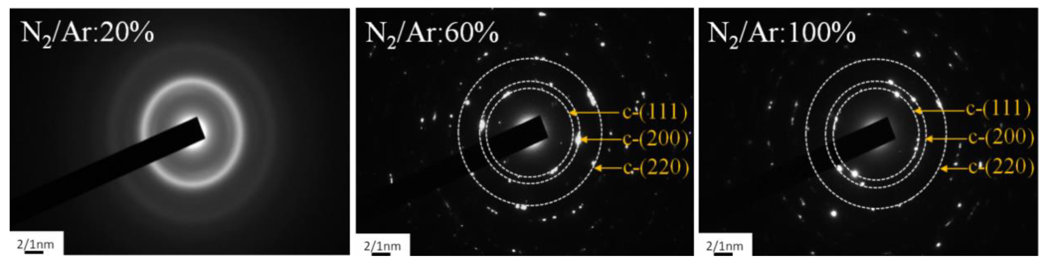
Figure 2 presents the SAED images obtained using a transmission electron microscope (TEM) from CrAlN layers formed under N2/Ar flow ratios of 20%, 60%, and 100%. The SAED patterns clearly indicate the amorphous structure of the CrAlN layers formed under an N2/Ar flow ratio of 20%. Increasing the nitrogen content beyond that point caused a structural transformation from amorphous to crystalline. Note that these results are in good agreement with our GIXRD results.
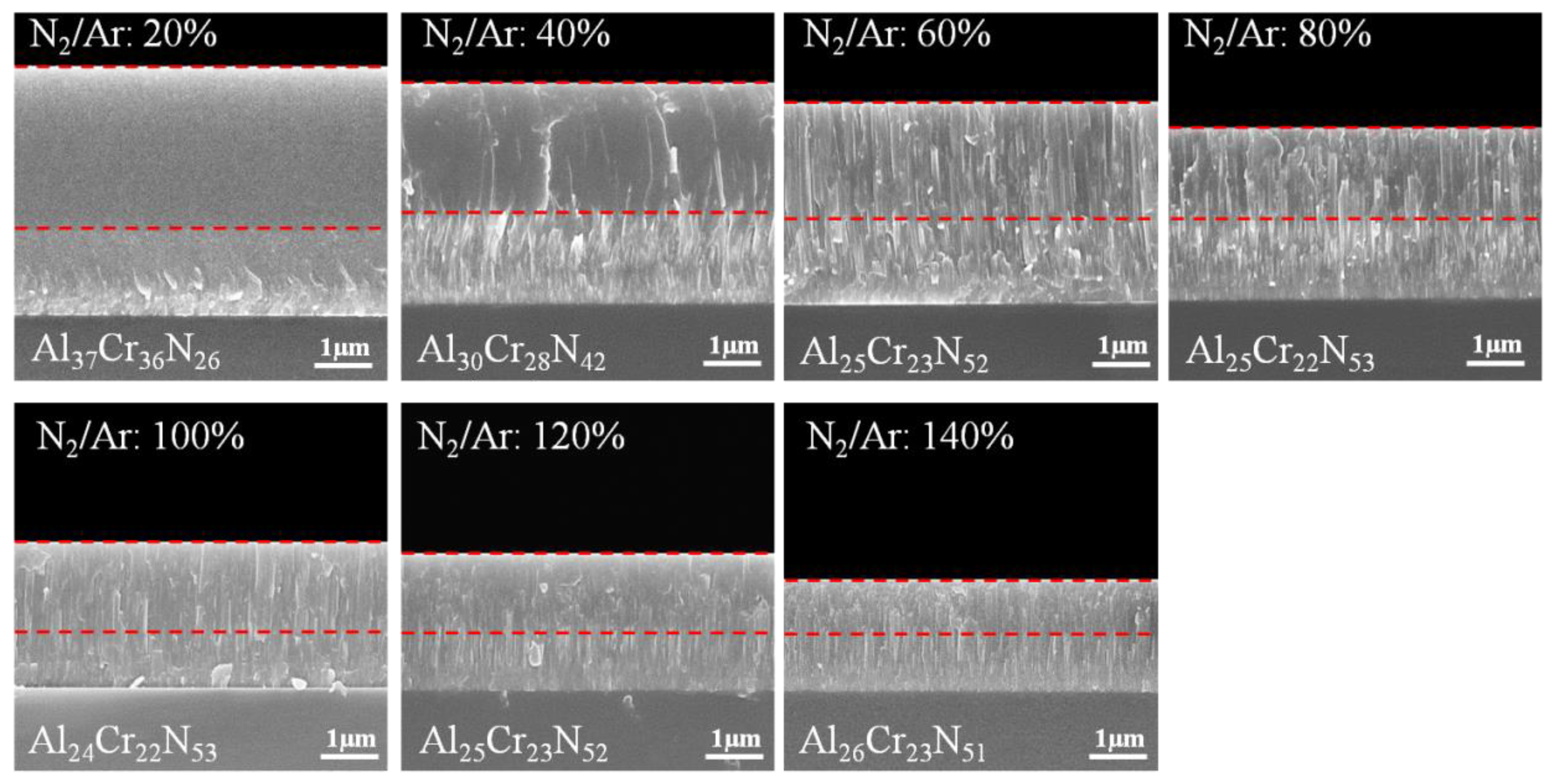
Figure 3 presents cross-sectional SEM images of coatings deposited under various N2/Ar flow ratios. The red-dotted line demarcates the CrAlN top layer. Under an N2/Ar flow ratio of <40%, no columnar-type structures were observed in the CrAlN. Under an N2/Ar flow ratio >40%, all of the CrAlN layers exhibited columnar-type structures. When the nitrogen content was increased (from 20% to 140%), the thickness of the CrAlN layer decreased from 2.86 to 0.97 μm and the deposition rate decreased from 71.5 to 24.3 nm/min. This was partly due to the fact that the sputtering rate of nitrided compounds is lower than that of metals [27]. Furthermore, the Me–N layers produced secondary electron emission yields higher than the metal targets, which further lower the sputtering yield of the targets [28].
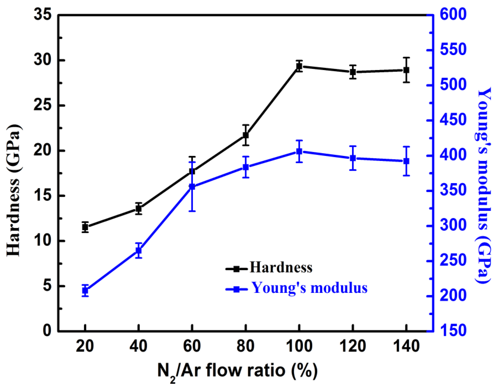
Figure 4 presents the hardness and Young’s modulus of CrAlN layers formed under various N2/Ar flow ratios. The highest hardness value (29.3 ± 0.6 GPa) and Young’s modulus (406.1 ± 15 GPa) were obtained when the N2/Ar flow ratio was 100%. The hardness values of all of the samples presented characteristic slopes in the linear fitting plot. There was a strong positive correlation between N2/Ar flow ratios (from 20% to 80%) with hardness values (from 11.5 ± 0.5 to 21.7 ± 1.3 GPa) and with Young’s modulus (from 207.9 ± 7 to 383.7 ± 14 GPa), due to the replacement of a large number of Me−Me bonds with Me−N bonds in the CrAlN film. At N2/Ar flow ratios exceeding 100%, the samples became saturated with nitrogen, such that the composition, crystal structure, and corresponding hardness and Young’s modulus of the CrAlN film did not change significantly. When the N2/Ar flow ratio was increased from 20% to 140%, the residual stress decreased from −0.5 to −2.8 GPa. Note that residual stress value is strongly related to film hardness. To assess the suitability of coatings for tribological applications, we calculated the deformation relative to yielding (H/E) and resistance to plastic indentation (H3/E2) ratios based on the nanoindentation results. Generally, the H/E and H3/E2 ratios are proportional to plastic deformation resistance [29]. The average H/E and H3/E2 ratios are summarized in Table 3.
Lc1 is commonly defined as the load required to peel a film off of a given substrate, as determined by the analysis of scratch morphology. As shown in Table 3, increasing the N2/Ar flow ratio from 20% to 140% decreased the Lc1 value from 54.6 to 41.8 N. This weak correlation between Lc1 values and N2/Ar flow ratios can be attributed to the modulation of the interlayer structure and an increase in residual stress in the coatings following an increase in the N2/Ar flow ratio.
The tribological properties of the coatings depend on multiple parameters including, the microstructure, grain size, density, surface quality, and residual stress in the coatings. Table 3 lists the coefficient of friction (COF) and average wear rates of each coating. Increasing the N2/Ar flow ratio from 20% to 140% increased the average COF from 0.7 to 0.8. The highest wear rates (9.4 × 10⁻⁶ mm3·N−1·m−1) were observed in samples formed under N2/Ar flow ratios of less than 40%, due to the lowest hardness (11.5 GPa) and larger grain size of those films. As shown in 
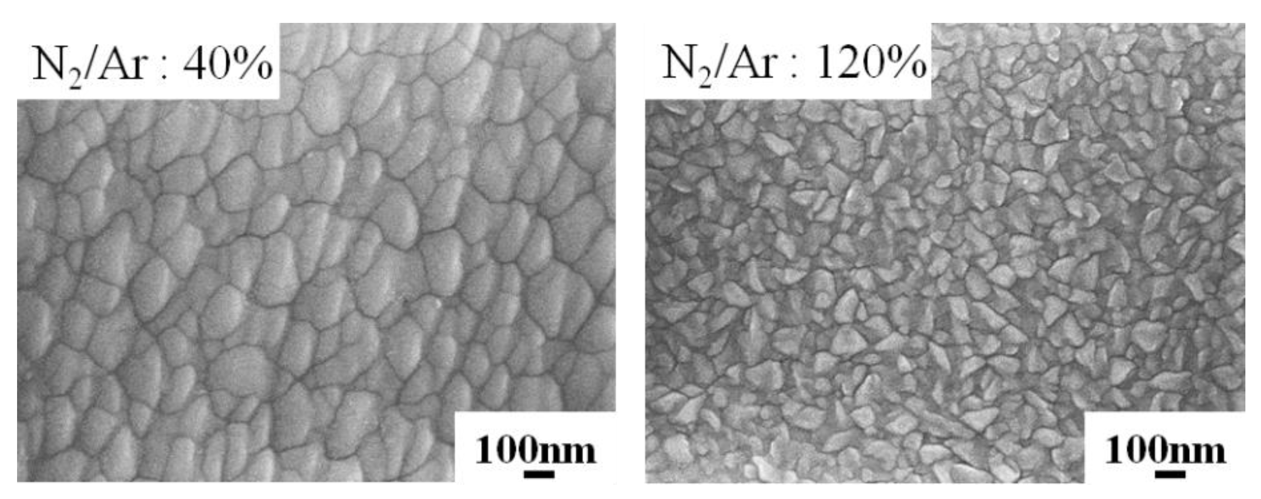
Figure 5, the grains in the CrAlN layer formed under an N2/Ar flow ratio of 40% were larger than those formed under an N2/Ar flow ratio of 120%. Wasekar et al. [30] reported a continuous decrease in the wear rate with a decrease in grain size. Increasing the N2/Ar flow ratio beyond 50% decreased the wear rate from 3.53 × 10⁻⁶ to 2.45 × 10⁻⁶ mm3·N−1·m−1, due to improvements in film hardness and tribo-chemical reactions at friction interfaces [31]. The coatings with the highest nitrogen composition presented good wear resistance as well as the highest H/E and H3/E2 ratios [32]. In this section, we observed the effects of N2/Ar flow ratio on the composition, crystal structure, and mechanical properties of CrAlN layers prepared via HiPIMS. The best mechanical properties were obtained with the N2/Ar ratio fixed at 100%. Note however, that the interpretation of these results may be best achieved using previously reported data. Wang et al. [31] reported that sharp increases in H values (from 14.0 to 22.0 GPa) and E values (from 149.9 to 198.3 GPa) occurred independently from the N2/Ar flow ratio. Greczynski et al. [33] and Hurkmans et al. [34] reported similar changes in hardness with increases in the nitrogen content in the CrNx films.

3.2. Effects of Bias Voltage on CrAlN Layers

In this section, we examine the effects of bias voltage on the structure and mechanical properties of CrAlN layers. Table 4 lists the chemical composition of CrAlN layers formed under various bias voltages. Increasing the negative bias voltage from −30 to −150 V slightly increased the Al content (from 23.8 to 25.6 at.%) and the Al/Cr ratio (from 1.09 to 1.22). These findings are in line with those in previous reports [18]. Previous studies have reported that increasing the bias voltage could decrease the Al content in the coating, due to the fact that relatively light Al atoms are more susceptible to re-sputtering by impinging ions than are Cr atoms. The discrepancy between the results in that study and the current study can be attributed to the Al/Cr ratio of the target. Note that when using AlCr alloy targets with a higher Al content, the number of discharged Al ions/atoms exceeds the number of Cr ions/atoms [35]. In contrast, using an AlCr alloy target with lower Al content under a moderate bias voltage promotes the mobility and diffusion of the Al atoms on the film surface [36]. No significant differences in terms of N/(Al+Cr) ratio was observed, which indicates that the nitrogen content was unaffected by bias voltage.
Figure 6 presents XRD patterns of CrAlN layers deposited under various bias voltages. As expected, the crystalline microstructure matched the NaCl-B1 structure (FCC) of chromium nitride. Increasing the bias voltage from −30 to −90 V initially led to an increase and then a subsequent decrease in the ratio of I(111)/I(200), which can be attributed to the thickness of the CrAlN coating [37]. Pelleg et al. [38] reported that the tendency toward a specific orientation can be explained by strain and surface energy. Coatings of greater thicknesses tend toward a (111) orientation, due to the effects of strain energy, whereas thinner coatings tend toward a (200) orientation. Increasing the bias voltage from −120 to −150 V decreased the ratio of I(111)/I(200). This is an indication that the strain energy increased rapidly to become the dominant factor (i.e., exceeding surface energy). This can be attributed to the higher intrinsic residual stress under higher bias voltages, which can have a direct effect on 200 texture [18]. As shown in Table 5, increasing the bias voltage from −30 to −150 V increased the lattice parameter of the CrAlN layer from 0.4143 to 0.4195 nm as well as the microstrain values from 5.06 × 10⁻³ to 6.78 × 10⁻³. XRD data revealed left shift in the diffraction peaks indicating the presence of residual tensile stress. A further increase in the negative bias provoked a broadening of the peaks (due to presence of inhomogeneous residual stress) and a pronounced decrease in intensities [28,39].
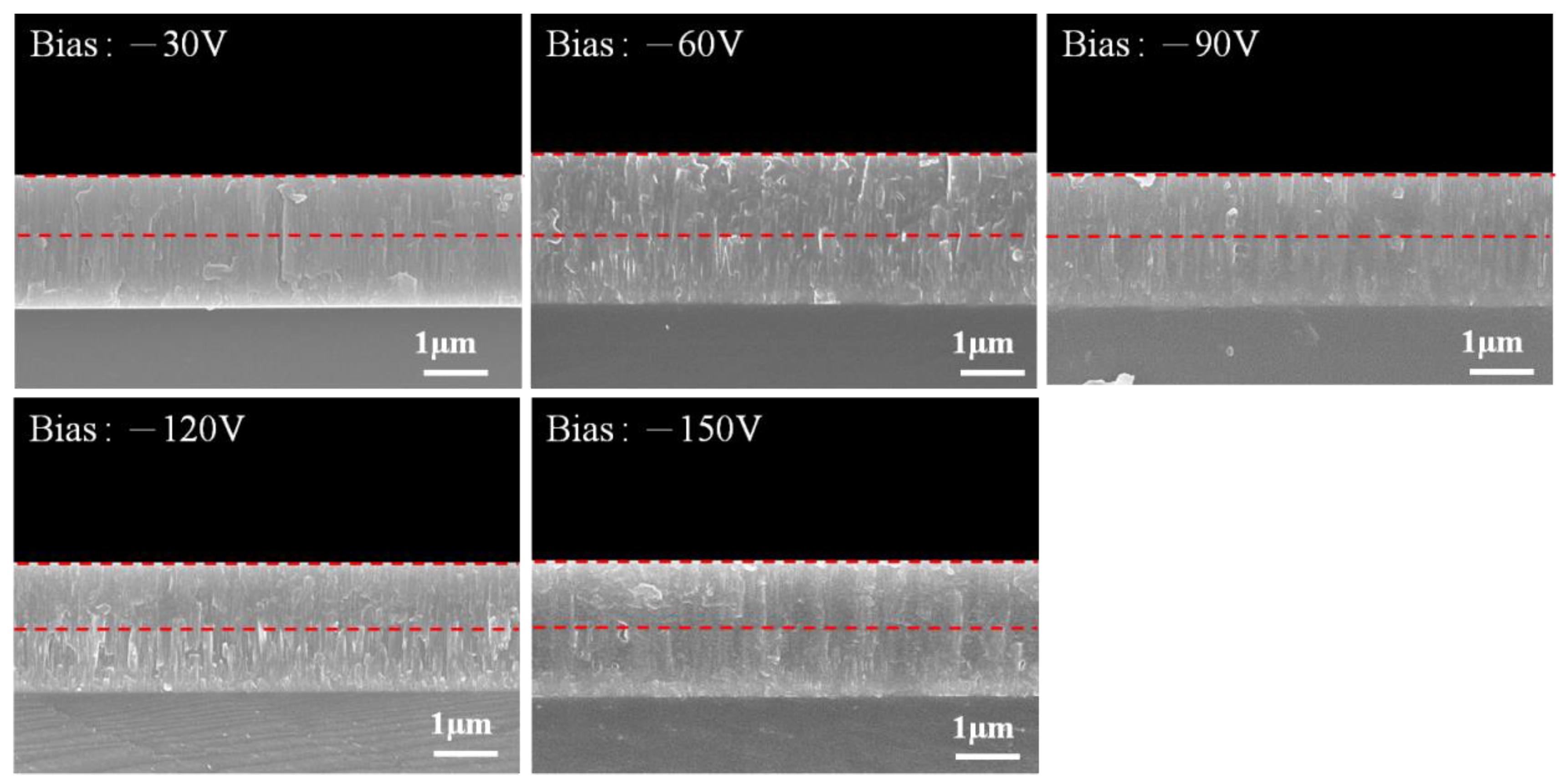
Figure 7 presents cross-sectional SEM images of coatings deposited under various bias voltages. Increasing the bias voltage from −30 to −90 V increased the deposition rate of the coating layer (from 29.2 to 30.3 nm/min) as well as the ultimate thickness (from 1.17 to 1.21 μm). Further increasing the bias voltage to −150 V led to a decrease not only in the deposition rate of the coating layer to 28.2 nm/min but also in the ultimate thickness to 1.13 μm. Under lower bias voltages, the atoms were at lower energy levels, which facilitated their deposition on the growing surface. Increasing the bias voltage to −90 V increased the kinetic energy of the highly ionized Cr and Al atoms arriving at the substrate, resulting in the re-sputtering of a larger number of atoms, which suppressed the growth of the film (i.e., a lower overall rate of deposition) [40].
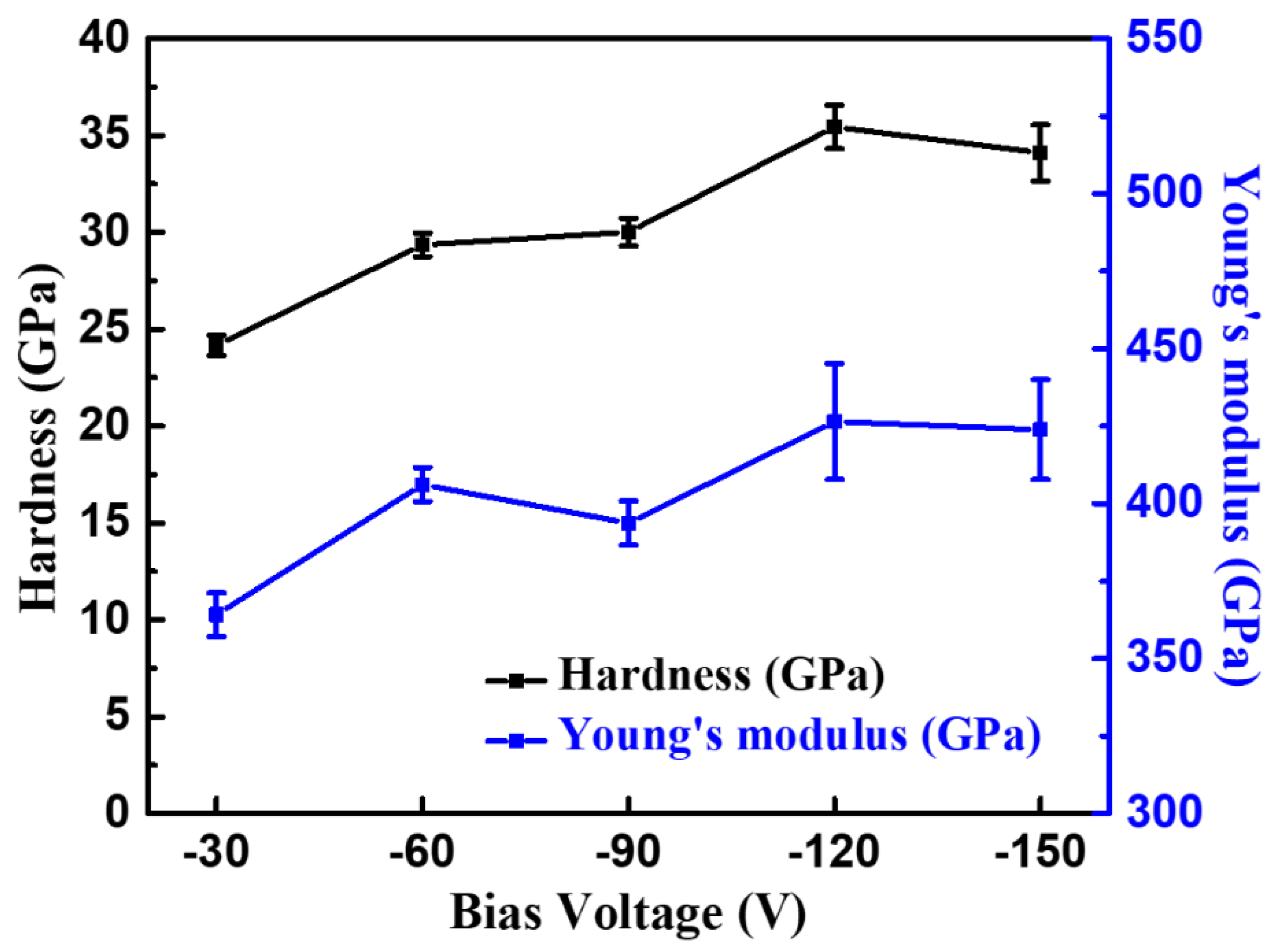
Figure 8 presents the hardness and Young’s modulus of CrAlN films obtained under various bias voltages. Increasing the bias voltage to beyond −90 V led to an increase in hardness (≈35 GPa) and Young’s modulus, due to the effects of grain size and residual stress in the coating. The crystallite sizes listed in Table 6 were calculated from the (111) and (200) planes. Increasing the bias voltage (from −30 to −150 V) decreased the crystallite sizes from 16.8 to 10.6 nm on the (111) plane and from 13.9 to 7.4 nm on the (200) plane. It has previously been reported that increasing the energy of incident ions generates a larger number of defects on the surface of growing films, which provide a larger number of nucleation sites and a corresponding increase in the number of grains (i.e., more grains of smaller size) [41]. Increasing the bias voltage was shown to increase the residual stresses in the coatings from −1.3 to −3.1 GPa, due to high defect densities induced by ion bombardment [42].
As shown in Table 6, increasing the bias voltage from −30 to −150 V increased the Lc1 values (from 39.3 to 42.8 N) as well as the residual stress. Yang et al. [43] reported that the adhesion properties of coatings are closely related to the density of the film and residual compressive stress. Low bias voltages (−30 V) inevitably lead to weak adhesion strength, due to the resulting low density of the coating. Note that adhesion performance can be undermined by excessive residual stress under higher bias voltages (exceeding −60 V). When the bias voltage was −60 V, the film exhibited a maximum Lc1 value of 46.6 N.
Table 6 also lists the COFs and average wear rates of each coating under various bias voltages. Note that the average COF values remained constant (~0.74) despite variations in bias voltage. Iram et al. [44] reported that wear rates are inversely proportional to hardness values and the formation of metal oxides. In this study, increasing the bias voltage from −30 V up to −120 V was shown to decrease the wear rate from 3.02 × 10⁻⁶ to 2.11 × 10⁻⁶ mm3·N−1·m−1. Note that increasing the bias voltage to −150 V led to increases in the H/E and H3/E2 ratios. Increasing the bias voltage was also shown to decrease the rate of wear to 2.89×10⁻⁶ mm3·N−1·m−1, under the effects of increased residual stress in the coating.

4. Conclusions

Our primary objective in this study was to elucidate the effects of N2/Ar flow ratios and bias voltages on the properties of CrAlN layers deposited using HiPIMS. The conclusions are outlined in the following:
1. Increasing the N2/Ar flow ratio beyond 40% transformed the coatings from amorphous to crystalline. Increasing the N2/Ar flow ratio was also shown to decrease the deposition rate, which led to structural densification and a decrease in coating thickness, due to the fact that the sputtering rate of nitrided compounds is lower than that of metals. The hardness of the coatings ranged from 11.5 to 29.3 GPa, depending on the nitrogen concentration. This can be attributed to the stoichiometric composition and microstructure (decreased crystallite size) of the coatings.
2. Increasing the bias voltage decreased the deposition rate and the size of crystallites in the CrAlN layer, which led to a corresponding increase in hardness and residual stress. The maximum hardness achieved in this study was 35.4 GPa.
3. Increasing the N2/Ar flow ratio from 0% to 100% and the bias voltage from −30 to −120 V led to a decrease in the wear rate of the coatings from 9.4 × 10⁻⁶ to 2.11 × 10⁻⁶ mm3·N−1·m−1. This can be attributed to increases in hardness, H/E ratio, and H3/E2 ratio as well as a reduction in grain size. The adhesion of the coatings to the substrate was relatively high, withstanding critical loads (in scratch testing) of 40–50 N.

Author Contributions

J.-F.T.: writing—original draft, writing—review & editing. C.-Y.L.: methodology, investigation. F.-C.Y.: methodology, resources. C.-L.C.: conceptualization, supervision, writing—review & editing. All authors have read and agreed to the published version of the manuscript.

Funding

This research was funded by the Ministry of Science and Technology, Taiwan, R.O.C, grant number [MOST 107-2622-E-131-001-CC2], [MOST 106-2218-E-131-003], and [MOST 107-2221-E-131-003].

Acknowledgments

The authors gratefully acknowledge the use of the FE-EPMA (JXA-iHP200F) apparatus at the Instrument Center of National Tsing Hua University.

Conflicts of Interest

The authors declare that they have no known competing financial interests or personal relationships that could have appeared to influence the work reported in this paper.

References

  1. Dubey, P.; Arya, V.; Srivastava, S.; Singh, D.; Chandra, R. Effect of nitrogen flow rate on structural and mechanical properties of Zirconium Tungsten Nitride (Zr–W–N) coatings deposited by magnetron sputtering. Surf. Coat. Technol. 2013, 236, 182–187. [Google Scholar] [CrossRef]
  2. Forsén, R.; Johansson, M.; Odén, M.; Ghafoor, N. Effects of Ti alloying of AlCrN coatings on thermal stability and oxidation resistance. Thin Solid Films 2013, 534, 394–402. [Google Scholar] [CrossRef] [Green Version]
  3. Tatemizo, N.; Imada, S.; Miura, Y.; Yamane, H.; Tanaka, K. Electronic structure of AlCrN films investigated using various photoelectron spectroscopies and ab initio calculations. J. Phys. Condens. Matter 2017, 29, 085502. [Google Scholar] [CrossRef] [PubMed]
  4. Shimizu, T.; Komiya, H.; Watanabe, T.; Teranishi, Y.; Nagasaka, H.; Morikawa, K.; Yang, M. HIPIMS deposition of TiAlN films on inner wall of micro-dies and its applicability in micro-sheet metal forming. Surf. Coat. Technol. 2014, 250, 44–51. [Google Scholar] [CrossRef]
  5. Paulitsch, J.; Schenkel, M.; Zufraß, T.; Mayrhofer, P.H.; Münz, W.-D. Structure and properties of high power impulse magnetron sputtering and DC magnetron sputtering CrN and TiN films deposited in an industrial scale unit. Thin Solid Films 2010, 518, 5558–5564. [Google Scholar] [CrossRef]
  6. Bobzin, K.; Lugscheider, E.; Nickel, R.; Bagcivan, N.; Krämer, A. Wear behavior of Cr1–xAlxN PVD-coatings in dry running conditions. Wear 2007, 263, 1274–1280. [Google Scholar] [CrossRef]
  7. Chang, Y.-Y.; Weng, S.-Y.; Chen, C.-H.; Fu, F.-X. High temperature oxidation and cutting performance of AlCrN, TiVN and multilayered AlCrN/TiVN hard coatings. Surf. Coat. Technol. 2017, 332, 494–503. [Google Scholar] [CrossRef]
  8. Chen, W.; Zheng, J.; Lin, Y.; Kwon, S.; Zhang, S. Comparison of AlCrN and AlCrTiSiN coatings deposited on the surface of plasma nitrocarburized high carbon steels. Appl. Surf. Sci. 2015, 332, 525–532. [Google Scholar] [CrossRef]
  9. Gilewicz, A.; Jedrzejewski, R.; Myslinski, P.; Warcholinski, B. Structure, Morphology, and Mechanical Properties of AlCrN Coatings Deposited by Cathodic Arc Evaporation. J. Mater. Eng. Perform. 2019, 28, 1522–1531. [Google Scholar] [CrossRef] [Green Version]
  10. Tillmann, W.; Kokalj, D.; Stangier, D.; Paulus, M.; Sternemann, C.; Tolan, M. Investigation of the influence of the vanadium content on the high temperature tribo-mechanical properties of DC magnetron sputtered AlCrVN thin films. Surf. Coat. Technol. 2017, 328, 172–181. [Google Scholar] [CrossRef]
  11. Endrino, J.; Fox-Rabinovich, G.; Reiter, A.; Veldhuis, S.; Galindo, R.E.; Albella, J.; Marco, J. Oxidation tuning in AlCrN coatings. Surf. Coat. Technol. 2007, 201, 4505–4511. [Google Scholar] [CrossRef]
  12. Tang, J.-F.; Lin, C.-Y.; Yang, F.-C.; Tsai, Y.-J.; Chang, C.-L. Effects of nitrogen-argon flow ratio on the microstructural and mechanical properties of AlCrN coatings prepared using high power impulse magnetron sputtering. Surf. Coat. Technol. 2020, 386, 125484. [Google Scholar] [CrossRef]
  13. Wang, Y.; Lee, J.-W.; Duh, J.-G. Mechanical strengthening in self-lubricating CrAlN/VN multilayer coatings for improved high-temperature tribological characteristics. Surf. Coat. Technol. 2016, 303, 12–17. [Google Scholar] [CrossRef]
  14. Jiang, X.; Yang, F.-C.; Chen, W.-C.; Lee, J.-W.; Chang, C.-L. Effect of nitrogen-argon flow ratio on the microstructural and mechanical properties of AlSiN thin films prepared by high power impulse magnetron sputtering. Surf. Coat. Technol. 2017, 320, 138–145. [Google Scholar] [CrossRef]
  15. Mahato, P.; Singh, R.; Pathak, L.; Mishra, S.K. Effect of nitrogen on mechanical, oxidation and structural behaviour of Ti–Si–B–C–N nanocomposite hard coatings deposited by DC sputtering. Surf. Interface Anal. 2016, 48, 1080–1089. [Google Scholar] [CrossRef]
  16. Chen, Y.-I.; Zheng, Y.-Z.; Chang, L.-C.; Liu, Y.-H. Effect of Bias Voltage on Mechanical Properties of HiPIMS/RFMS Cosputtered Zr–Si–N Films. Materials 2019, 12, 2658. [Google Scholar] [CrossRef] [Green Version]
  17. Biswas, B.; Purandare, Y.; Khan, I.; Hovsepian, P.E. Effect of substrate bias voltage on defect generation and their influence on corrosion and tribological properties of HIPIMS deposited CrN/NbN coatings. Surf. Coat. Technol. 2018, 344, 383–393. [Google Scholar] [CrossRef]
  18. Lomello, F.; Sanchette, F.; Schuster, F.; Tabarant, M.; Billard, A. Influence of bias voltage on properties of AlCrN coatings prepared by cathodic arc deposition. Surf. Coat. Technol. 2013, 224, 77–81. [Google Scholar] [CrossRef]
  19. Kim, U.-J.; Eom, S.H.; Wada, M. Thermal decomposition of native cellulose: Influence on crystallite size. Polym. Degrad. Stab. 2010, 95, 778–781. [Google Scholar] [CrossRef]
  20. Warcholinski, B.; Gilewicz, A.; Lupicka, O.; Kuprin, A.; Tolmachova, G.; Ovcharenko, V.; Kolodiy, I.; Sawczak, M.; Kochmanska, A.; Kochmanski, P. Structure of CrON coatings formed in vacuum arc plasma fluxes. Surf. Coat. Technol. 2017, 309, 920–930. [Google Scholar] [CrossRef]
  21. Oliver, W.C.; Pharr, G.M. An improved technique for determining hardness and elastic modulus using load and displacement sensing indentation experiments. J. Mater. Res. 1992, 7, 1564–1583. [Google Scholar] [CrossRef]
  22. Chen, S.-F.; Kuo, Y.-C.; Wang, C.-J.; Huang, S.-H.; Lee, J.-W.; Chan, Y.-C.; Chen, H.-W.; Duh, J.-G.; Hsieh, T.-E. The effect of Cr/Zr chemical composition ratios on the mechanical properties of CrN/ZrN multilayered coatings deposited by cathodic arc deposition system. Surf. Coat. Technol. 2013, 231, 247–252. [Google Scholar] [CrossRef]
  23. Hiratsuka, M.; Azuma, A.; Nakamori, H.; Kogo, Y.; Yukimura, K. Extraordinary deposition rate of diamond-like carbon film using HIPIMS technology. Surf. Coat. Technol. 2013, 229, 46–49. [Google Scholar] [CrossRef]
  24. Liu, H.; Tang, J.-F.; Wang, X.; Li, W.; Chang, C.-L. Effects of nitrogen-argon flow ratio on the microstructural and mechanical properties of TiAlSiN/CrN multilayer coatings prepared using high power impulse magnetron sputtering. J. Vac. Sci. Technol. A 2019, 37, 051501. [Google Scholar] [CrossRef]
  25. Li, Q.; Cheng, X.; Gong, D.; Ye, W. Effect of N2 flow rate on structural and infrared properties of multi-layer AlCrN/Cr/AlCrN coatings deposited by cathodic arc ion plating for low emissivity applications. Thin Solid Films 2019, 675, 74–85. [Google Scholar] [CrossRef]
  26. Ferreira, F.; Oliveira, J.; Cavaleiro, A. CrN thin films deposited by HiPIMS in DOMS mode. Surf. Coat. Technol. 2016, 291, 365–375. [Google Scholar] [CrossRef]
  27. Han, Z.; Tian, J.; Lai, Q.; Yu, X.; Li, G. Effect of N2 partial pressure on the microstructure and mechanical properties of magnetron sputtered CrNx films. Surf. Coat. Technol. 2003, 162, 189–193. [Google Scholar] [CrossRef]
  28. Forniés, E.; Galindo, R.E.; Sánchez, O.; Albella, J. Growth of CrNx films by DC reactive magnetron sputtering at constant N2/Ar gas flow. Surf. Coat. Technol. 2006, 200, 6047–6053. [Google Scholar] [CrossRef]
  29. Warcholinski, B.; Gilewicz, A.; Kuprin, A.; Tolmachova, G.; Ovcharenko, V.; Kuznetsova, T.; Zubar, T.; Khudoley, A.; Chizhik, S. Mechanical properties of Cr-ON coatings deposited by cathodic arc evaporation. Vacuum 2018, 156, 97–107. [Google Scholar] [CrossRef]
  30. Wasekar, N.P.; Haridoss, P.; Seshadri, S.; Sundararajan, G. Sliding wear behavior of nanocrystalline nickel coatings: Influence of grain size. Wear 2012, 296, 536–546. [Google Scholar] [CrossRef]
  31. Li, B.-S.; Wang, T.-G.; Ding, J.; Cai, Y.; Shi, J.; Zhang, X. Influence of N2/Ar flow ratio on microstructure and properties of the AlCrSiN coatings deposited by high-power impulse magnetron sputtering. Coatings 2018, 8, 3. [Google Scholar] [CrossRef] [Green Version]
  32. Warcholinski, B.; Gilewicz, A.; Kuznetsova, T.; Zubar, T.; Chizhik, S.; Abetkovskaia, S.; Lapitskaya, V. Mechanical properties of Mo (C) N coatings deposited using cathodic arc evaporation. Surf. Coat. Technol. 2017, 319, 117–128. [Google Scholar] [CrossRef]
  33. Greczynski, G.; Jensen, J.; Hultman, L. Films Prepared by DC Magnetron Sputtering and High-Power Pulsed Magnetron Sputtering: A Comparative Study. IEEE Trans. Plasma Sci. 2010, 38, 3046–3056. [Google Scholar] [CrossRef] [Green Version]
  34. Hurkmans, T.; Lewis, D.; Brooks, J.; Münz, W.-D. Chromium nitride coatings grown by unbalanced magnetron (UBM) and combined arc/unbalanced magnetron (ABS™) deposition techniques. Surf. Coat. Technol. 1996, 86, 192–199. [Google Scholar] [CrossRef]
  35. Sabitzer, C.; Paulitsch, J.; Kolozsvári, S.; Rachbauer, R.; Mayrhofer, P. Influence of bias potential and layer arrangement on structure and mechanical properties of arc evaporated Al–Cr–N coatings. Vacuum 2014, 106, 49–52. [Google Scholar] [CrossRef]
  36. Lv, Y.; Ji, L.; Liu, X.; Li, H.; Zhou, H.; Chen, J. Influence of substrate bias voltage on structure and properties of the CrAlN films deposited by unbalanced magnetron sputtering. Appl. Surf. Sci. 2012, 258, 3864–3870. [Google Scholar] [CrossRef]
  37. Nouveau, C.; Djouadi, M.; Banakh, O.; Sanjinés, R.; Lévy, F. Stress and structure profiles for chromium nitride coatings deposited by rf magnetron sputtering. Thin Solid Films 2001, 398, 490–495. [Google Scholar] [CrossRef]
  38. Pelleg, J.; Zevin, L.; Lungo, S.; Croitoru, N. Reactive-sputter-deposited TiN films on glass substrates. Thin Solid Films 1991, 197, 117–128. [Google Scholar] [CrossRef]
  39. Warcholinski, B.; Kuznetsova, T.; Gilewicz, A.; Zubar, T.; Lapitskaya, V.; Chizhik, S.; Komarov, A.; Komarova, V.; Kuprin, A.; Ovcharenko, V.; et al. Structural and mechanical properties of Zr-Si-N coatings deposited by arc evaporation at different substrate bias voltages. J. Mater. Eng. Perform. 2018, 27, 3940–3950. [Google Scholar] [CrossRef] [Green Version]
  40. Rong, S.; He, J.; Wang, H.; Tian, C.; Guo, L.; Fu, D. Effects of bias voltage on the structure and mechanical properties of thick CrN coatings deposited by mid-frequency magnetron sputtering. Plasma Sci. Technol. 2009, 11, 38. [Google Scholar] [CrossRef]
  41. Lee, J.-W.; Tien, S.-K.; Kuo, Y.-C. The effects of pulse frequency and substrate bias to the mechanical properties of CrN coatings deposited by pulsed DC magnetron sputtering. Thin Solid Films 2006, 494, 161–167. [Google Scholar] [CrossRef]
  42. Kong, Q.; Ji, L.; Li, H.; Liu, X.; Wang, Y.; Chen, J.; Zhou, H. Influence of substrate bias voltage on the microstructure and residual stress of CrN films deposited by medium frequency magnetron sputtering. Mater. Sci. Eng. B 2011, 176, 850–854. [Google Scholar] [CrossRef]
  43. Chen, X.; Xi, Y.; Meng, J.; Pang, X.; Yang, H. Effects of substrate bias voltage on mechanical properties and tribological behaviors of RF sputtered multilayer TiN/CrAlN films. J. Alloys Compd. 2016, 665, 210–217. [Google Scholar] [CrossRef]
  44. Iram, S.; Cai, F.; Wang, J.; Zhang, J.; Liang, J.; Ahmad, F.; Zhang, S. Effect of Addition of Mo or V on the Structure and Cutting Performance of AlCrN-Based Coatings. Coatings 2020, 10, 298. [Google Scholar] [CrossRef] [Green Version]
Figure 1. Grazing incidence X-ray diffractometer (GIXRD) profiles of CrAlN layers as a function of N2/Ar flow ratio.
Coatings 10 00546 g001
Figure 2. Selected area electron diffraction (SAED) patterns of CrAlN layers formed under N2/Ar flow ratios of 20%, 60%, and 100%.
Coatings 10 00546 g002
Figure 3. Cross-sectional scanning electron microscope (SEM) images of coatings deposited under various N2/Ar flow ratios.
Coatings 10 00546 g003
Figure 4. Hardness and Young’s modulus of CrAlN layers deposited under various N2/Ar flow ratios.
Coatings 10 00546 g004
Figure 5. SEM images of CrAlN layers formed under N2/Ar flow ratios of 40% and 120%.
Coatings 10 00546 g005
Figure 6. GIXRD profiles of CrAlN layers formed under various bias voltages.
Coatings 10 00546 g006
Figure 7. Cross-sectional SEM images of coatings deposited under various bias voltages.
Coatings 10 00546 g007
Figure 8. Hardness and Young’s modulus of CrAlN layers deposited under various bias voltages.
Coatings 10 00546 g008
Table 1. N2/Ar flow ratios and corresponding effects on peak power density and concentrations of constituent elements in CrAlN coatings.
N2/Ar (%)Peak Power Density (kW/cm2)Atomic Ratio (at.%)Al/Cr RatioAl/(Al+Cr) Ratio xN/(Al+Cr) Ratio
AlCrNO
201.1637.936.125.60.401.050.510.34
401.2029.728.341.60.371.050.510.71
601.2624.722.752.30.281.080.521.11
801.4624.622.352.90.231.090.521.12
1001.5224.222.253.10.481.080.521.14
1201.5424.623.052.00.351.060.511.09
1401.6025.722.851.00.461.120.521.05
Table 2. Lattice parameters and texture coefficient of CrAlN layer under various N2/Ar flow ratios.
N2/Ar (%)Lattice Parameter (nm)Microstrain εTexture Coefficient Tc
(111)(200)(220)
600.41283.57 × 10−31.390.371.23
800.41434.07 × 10−31.260.521.22
1000.41565.01 × 10−31.010.961.03
1200.41705.33 × 10−30.871.031.09
1400.41874.80 × 10−30.981.120.89
Table 3. Mechanical properties of CrAlN coatings under various N2/Ar flow ratios.
N2/Ar (%)Hardness (GPa)Elastic Modulus (GPa)H/EH3/E2Lc1 (N)COFWear Rate (mm3·N−1·m−1)Residual Stress (GPa)
2011.5 ± 0.5208 ± 70.0550.03554.60.799.40 × 10−6−0.5
4013.5 ± 0.6265 ± 100.0500.03551.20.738.07 × 10−6−0.5
6017.7 ± 1.6356 ± 340.0490.04350.70.783.53 × 10−6−1.5
8021.7 ± 1.3383 ± 140.0560.06948.10.883.11 × 10−6−1.7
10029.3 ± 0.6406 ± 150.0720.15246.60.712.71 × 10−6−2.3
12028.7 ± 0.7397 ± 160.0720.14945.40.862.24 × 10−6−2.4
14028.9 ± 1.3392 ± 200.0730.15741.80.732.45 × 10−6−2.8
Table 4. Concentration of CrAlN coatings under various bias voltages.
Bias Voltage (V)Atomic Ratio (at.%)Al/Cr RatioAl/(Al+Cr) Ratio, xN/(Al+Cr) Ratio
AlCrNO
−3023.821.754.10.371.090.521.19
−6024.222.253.10.481.080.521.14
−9025.821.052.90.271.220.551.12
−12025.621.752.40.341.180.541.10
−15025.621.152.70.301.220.551.12
Table 5. Structural parameter values and texture coefficients in CrAlN layers created under various bias voltages.
Bias Voltage (V)Lattice Parameter (nm)Microstrain εTexture Coefficient Tc
(111)(200)(220)
−300.41435.06 × 10−30.511.510.97
−600.41565.01 × 10−31.010.961.03
−900.41626.57 × 10−30.921.290.78
−1200.41867.10 × 10−31.071.010.92
−1500.41956.78 × 10−31.041.060.88
Table 6. Mechanical properties of CrAlN coatings under various bias voltages.
Bias Voltage (V)Hardness (GPa)Elastic Modulus (GPa)H/EH3/E2Crystallite Size (nm)Lc1 (N)COFWear Rate (mm3·N−1·m−1)Residual Stress (GPa)
(111)(200)
−3024.1 ± 0.5364 ± 60.0660.10516.813.939.30.743.02 × 10−6−1.3
−6029.3 ± 0.6406 ± 50.0720.15214.111.046.60.712.71 × 10−6−2.3
−9030.1 ± 0.7400 ± 70.0760.17012.110.944.10.802.12 × 10−6−2.5
−12035.4 ± 1.1426 ± 180.0830.24412.08.043.60.722.11 × 10−6−2.9
−15034.1 ± 1.4423 ± 150.0810.22110.67.442.80.732.89 × 10−6−3.1

