Article

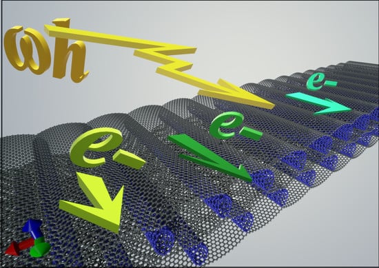
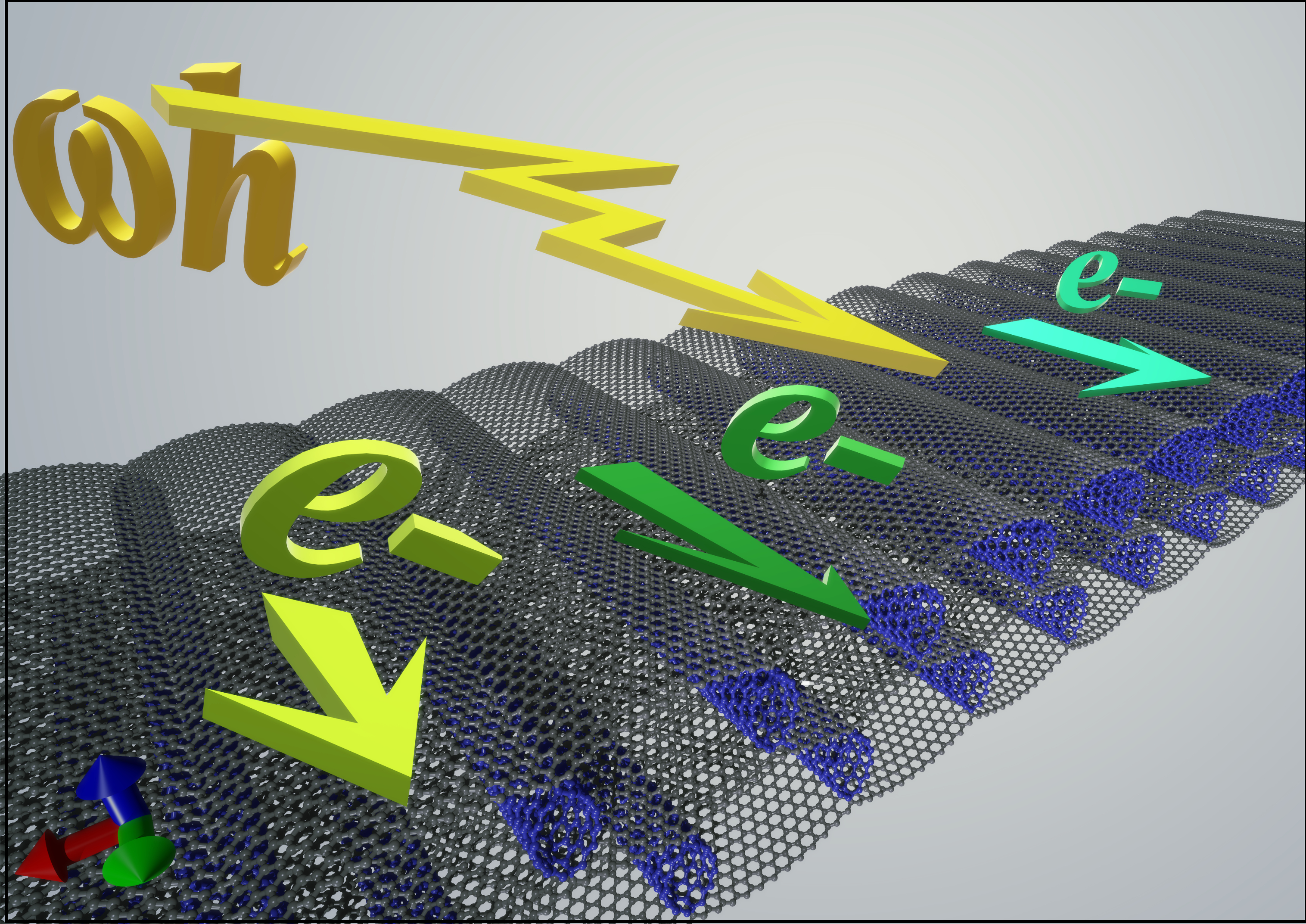
Electrical and Photovoltaic Properties of Layered Composite Films of Covalently Bonded Graphene and Single-Walled Carbon Nanotubes

by
Michael M. Slepchenkov
1,
Vadim V. Mitrofanov
1,
Igor S. Nefedov
2,3 and
Olga E. Glukhova
1,4,*
1
Department of Physics, Saratov State University, Astrakhanskaya street 83, 410012 Saratov, Russia
2
School of Electrical Engineering, Aalto University, P.O. Box 13000, 00076 Aalto, Finland
3
Faculty of Science, People’s Friendship University of Russia (RUDN University) 6 Miklukho-Maklaya St, 117198 Moscow, Russia
4
Laboratory of Biomedical Nanotechnology, I.M. Sechenov First Moscow State Medical University, Bolshaya Pirogovskaya street 2-4, 119991 Moscow, Russia
*
Author to whom correspondence should be addressed.
Coatings 2020, 10(4), 324; https://doi.org/10.3390/coatings10040324
Submission received: 3 March 2020 / Revised: 24 March 2020 / Accepted: 26 March 2020 / Published: 28 March 2020
(This article belongs to the Special Issue Photocatalytic Surfaces for Environmental Applications)

Abstract

:
In this paper, we present the results of a computational study of the electrical and photovoltaic properties of a perspective composite material; that is, layered composite films of covalently bonded graphene and single-walled carbon nanotubes (SWCNTs). The purpose of the study is to identify the topological patterns in controlling the electrical and photovoltaic properties of mono- and bilayer graphene/CNT composite films with a covalent bonding of a nanotube and graphene sheet, using in silico methods. This in silico study was carried out for the super-cells of mono- and bilayer graphene/CNT composite films with the CNTs (10,0) and (12,0) at distances between the nanotubes of 10 and 12 hexagons. This found that the type of conductivity of the nanotubes does not fundamentally affect the patterns of current flow in the graphene/CNT composite films. This control of the diameter of the nanotubes and the distance between them allows us to control the profile of the absorption spectrum of the electromagnetic waves in the range of 20–2000 nm. The control of the distance between the SWCNTs allows one to control the absorption intensity without a significant peak shift. This revealed that there is no obvious dependence of the integrated photocurrent on the distance between the nanotubes, and the photocurrent varies between 3%–4%.

Graphical Abstract

1. Introduction

Currently, a new composite material based on two-dimensional graphene and one-dimensional carbon nanotubes (CNTs) is of great interest to this study [1,2,3,4,5,6]. There are several structural varieties of this composite material, each differing in their methods of joining a CNT and graphene, as well as their mutual orientation [7]. One of the promising topological configurations of the graphene/CNT composite material is a two-dimensional film with a horizontal orientation of nanotubes connected to graphene through covalent bonds or through van der Waals forces [8,9,10,11,12]. New carbon composite structures have already demonstrated superiority over individual nanotubes and graphene in electrical, optical and electrochemical properties, providing new opportunities for developing promising applications based on these materials. The development of synthesis technology makes it possible to obtain graphene/CNT composite films with both ordered and disordered arrangements of multi-walled CNTs (MWCNTs) or single-walled CNTs (SWCNTs) connected to graphene via covalent bonds [8,9,10,11,12,13,14,15,16] or through van der Waals forces [17,18,19]. Moreover, CNTs can either be located on graphene [20,21,22,23], or be coated with graphene on top [24,25,26]. The diversity in the architecture of graphene/CNT composite films determines their wide range of applications.
Graphene/CNT composite films with oxidized graphene and CNTs bonded by van der Waals forces have improved electrochemical properties and can be used as a high-performance negative electrode in asymmetric supercapacitors [27]. It was found that the intercalation of a small amount of CNTs between oxidized graphene sheets leads to an excellent specific capacity of an obtained composite structure of 272 F·g−1 at a scanning speed of 5 mV·s-1. Coating such a composite structure with cobalt hydroxide Co(OH)2 allows us to further increase the specific capacity of the asymmetric supercapacitor based on the oxidized graphene/CNT composite film up to 310 F·g−1 [28]. Maarouf et al. showed that graphene/CNT composite films with graphene, deposited on a monolayer of self-organizing conducting SWCNTs, have a transparency of about 97% in the visible wavelength range [25]. Kholmanov et al. obtained composite films of a graphene monolayer deposited on a layer of ordered MWCNTs. These films showed strong anisotropy in optical transparency depending on the direction of polarization of the electromagnetic wave [12]. It was shown that with a light polarization parallel to the direction of the nanotube’s orientation, the transparency of graphene/MWCNT composite films is 75%–80% in the wavelength range of 400 to 1400 nm. With a light polarization perpendicular to the direction of the nanotube’s orientation, the transparency of the composite films is 87%–93% in the same wavelength range.
One of the new structural modifications of graphene/CNT composite films is a film with a covalent bonding of graphene and CNTs. Terrones et al. developed a self-assembly method for producing paper-like composite films consisting of alternating layers of oxidized graphene and various types of MWCNTs (pure and functionalized with boron and nitrogen). These oxidized graphene/MWCNTs composite films demonstrated excellent electronic properties [8]. The specific electrical resistivity of these composite films is 3·10−4 Ohm·cm, which is significantly less than the electrical resistivity of the MWCNT films (0.13 Ω·cm). Moreover, these composite films can be used as highly efficient field emission sources due to them having a threshold electric field with a strength of 0.55 V/μm, a field gain above 15.19·103, and operating currents up to 220 μA. Tour et al. developed an efficient technology for the production of highly conductive and transparent graphene/CNT composite films, called rebar graphene, by annealing copper substrates coated with functionalized CNTs. In this composite structure, the CNTs act as reinforcing bars to improve the mechanical strength and electrical conductivity of the graphene sheets [13]. The rebar graphene sheets have a transmittance of 95.8% at a wavelength of 550 nm and a surface resistance of 600 Ω·sq−1, which indicates a better performance than the folded bilayer graphene or CNT films with the same transparency. Similar graphene/CNT composite films were created by Kim et al. using the CVD method on a copper substrate coated with CNTs [10]. They have a surface resistance of 300 Ohm/sq with a transparency of 96.4%. Due to the alignment of the nanotubes on graphene, these composite structures possess improved current characteristics, which makes them a promising material for the design of field-effect transistors with a controlled gate.
At the same time, the photovoltaic properties of graphene/CNT composite films with a covalent bonding of CNTs and graphene are still poorly understood. The question of the influence of topology on the electrical properties of graphene/CNT materials remains open. The purpose of this work is to identify the topological patterns in controlling the electrical and photovoltaic properties of mono- and bilayer graphene/CNT composite films with a covalent bonding of a nanotube and graphene sheet using in silico methods. This work is a logical continuation of our earlier works [29,30], in which monolayer graphene/CNT composite structures were mostly considered. For bilayer graphene/CNT composite films, only a study of the electromechanical properties was previously carried out [30].

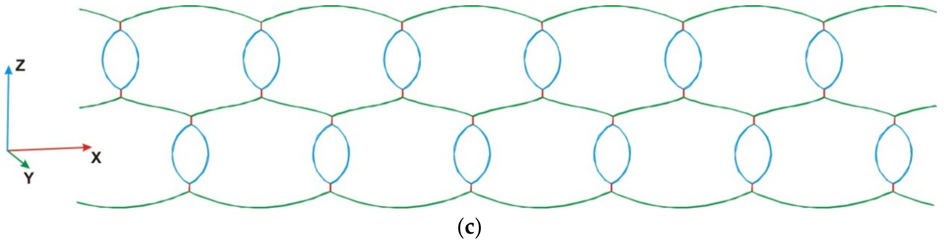
2. Atomistic Models of Layered Graphene/CNT Composite Films

To construct the super-cells of the mono- and bilayer graphene/CNT composite films under study, we used an original approach called the “magnifying glass method” [29]. As part of this approach, an atomistic model, in the form of a large fragment of graphene/CNT composite with a number of atoms of several tens of thousands, was constructed at the initial stage. Using the molecular dynamics method and empirical adaptive intermolecular reactive bond-order (AIREBO) potential [31], the atomic network of the object was optimized by minimizing its total energy. At the next stage, a smaller fragment was cut out from the middle part of the optimized composite structure, which was reoptimized in a periodic box using the self-consistent charge density functional tight-binding quantum method (SCC-DFTB) [32]. The sizes of the periodic box were also optimized to find a configuration that meets the minimum total energy. At the final stage, a super-cell was cut out from the previously optimized fragment, which was again optimized in the periodic box using the SCC-DFTB method. In this case, the optimization parameters were both the atom coordinates and box sizes.
In this work, in silico studies were carried out for the super-cells of mono- and bilayer graphene/CNT composite structures with the nanotubes (10,0) and (12,0) at distances between the tubes of 10 and 12 hexagons. It was previously shown [30] that the super-cells of the atomistic models of graphene/CNT composite structures formed by a semiconductor (10,0) and metal (12,0) SWCNTs at a distance between the adjacent SWCNTs of 10 and 12 hexagons are the most energetically favorable in both the cases of the mono- and bilayer composites. The heat of formation of these structures lies in the range of −1.12–−0.15 kcal/molatom. The constructed super-cells of the mono- and bilayer graphene/CNT structures are shown in Figure 1a by the example of composites with CNTs (12,0) and a distance of 12 hexagons between them. Figure 1b,c shows a general view of the mono- and bilayer graphene/CNT composite films constructed by translating the super-cells shown in Figure 1a. Table 1 shows the geometric characteristics of all the considered atomistic models of the super-cells of the mono- and bilayer graphene/CNT composite films based on the SWCNTs (10,0) and (12,0): the translation vectors Lx and Ly in the directions of the X (perpendicular to the axis of the nanotube) and Y (along the axis of the nanotube) axes, respectively, the distance between the adjacent nanotubes, rt-t, and the parameter a/b, characterizing the degree of deformation of the nanotubes, where a is the semi-major axis of the ellipse and b is the semi-minor axis of the ellipse, are shown in Figure 1a. As shown in Table 1, the degree of deformation of the nanotubes during the formation of the graphene/CNT composite is the same for all the types of atomistic models and is equal to ~ 1.64−1.66. The length of the graphene/CNT covalent bond is 1.61–1.62 Å in all cases. All calculations were carried out using the Kvazar [33] and DFTB+ software packages [34].

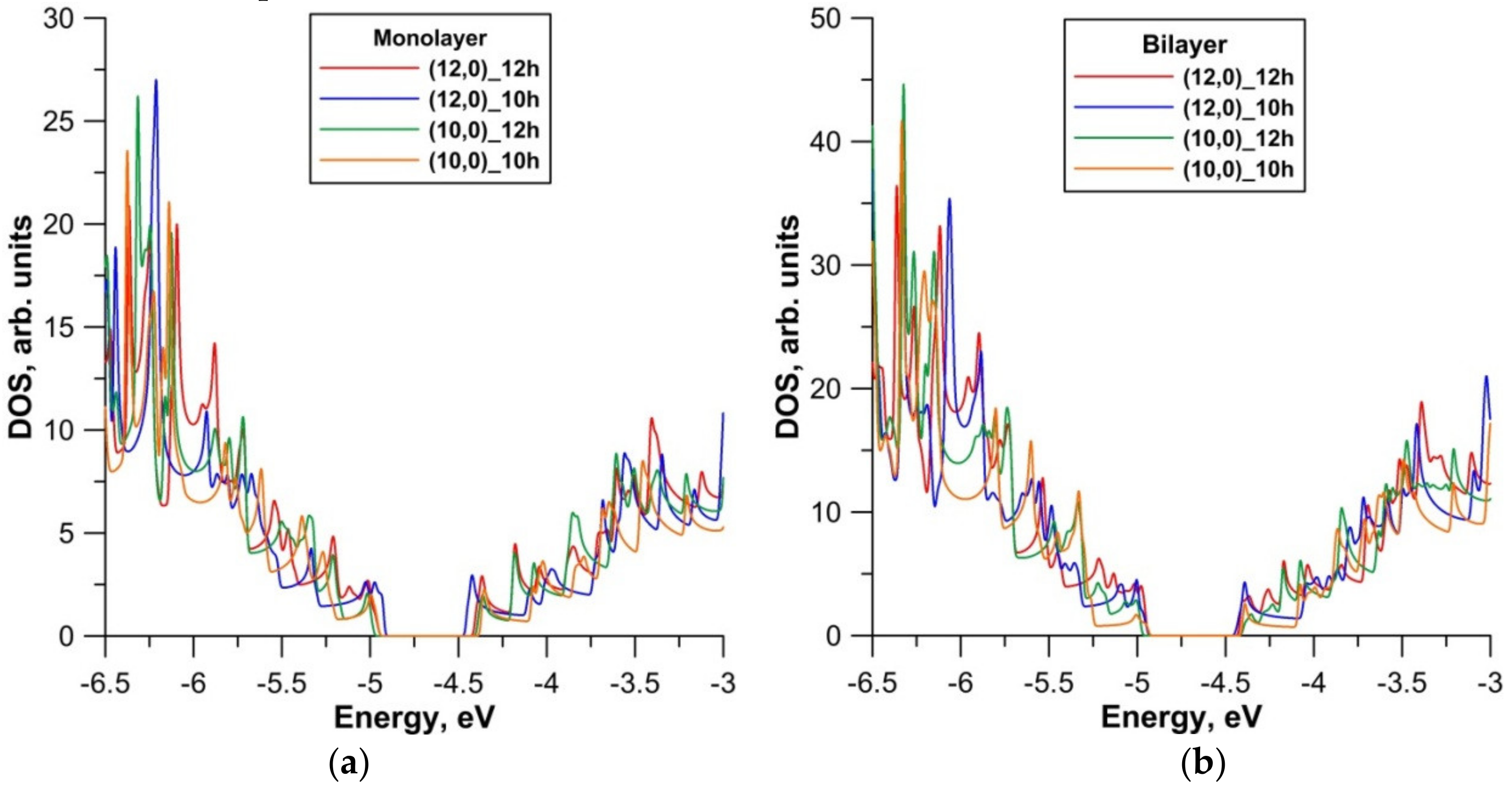
3. Electrical Properties of Layered Graphene/CNT Composite Films

To determine the type of conductivity of the graphene/CNT composite films under study, the distribution of the density of electronic states (DOS) was calculated using the SCC-DFTB method. The calculations were carried out in the sp-basis of atomic orbitals. The obtained DOS plots in the interval near the Fermi level are presented in Figure 2. Table 2 also presents the calculated values of the Fermi level, EF, and the energy gap, Egap, for all the considered topological variants of the graphene/CNT composite films.
From the data of Table 2 and Figure 2, one can see that the Fermi level for all the considered topological variants is approximately the same and amounts to −4.66–−4.69 eV. The energy gap between the valence and conduction bands is present in the band structure of all the studied atomistic models of graphene/CNT composite films and is in the range 0.47–0.59 eV. Therefore, regardless of the type of conductivity of the nanotube, all the considered graphene/CNT composite films are semiconductors. The energy gap for the composite films with CNTs (10,0) narrows and amounts to 0.57–0.59 eV relative to the energy gap of the individual CNTs (10,0), equal to 0.9 eV. In contrast, the energy gap of the composite films with CNTs (12,0) broadens to an interval of 0.47–0.54 eV, as compared with the individual CNTs (12,0), which are characterized by a metallic type of conductivity and have an energy gap of only 0.07 eV.
In order to identify the patterns of current flow in graphene/CNT composite films, the current–voltage characteristics were calculated for all the considered atomistic models. The current through the graphene/CNT composite film was calculated using the Landauer–Buttiker formula [35]
I = e T ( E ) d E f 1 ( E ) f 2 ( E ) ,
where T(E) is the transmission function, which determines the total quantum-mechanical transparency of the conducting structure over all the independent conduction channels for an electron with energy E; f1 and f2 are the Fermi–Dirac functions that characterize the energy levels of source and drain. When calculating the current–voltage characteristics, only one direction of current transfer was considered; that is, along the nanotubes, since there is no current in the perpendicular direction. The calculated families of the current–voltage characteristics of the mono- and bilayer graphene/CNT composite films are presented in Figure 3.
Figure 3 shows that in the case of the bilayer structures, the maximum current values at a voltage of 2.2 V are demonstrated by the graphene/CNT composite films with CNTs (12,0) and a distance of 12 hexagons between them, as well as the films with nanotubes (10,0) and a distance of 10 hexagons between them. In the case of the monolayer structures, the graphene/CNT composite films with CNTs (12,0) at a distance between them of 12 and 10 hexagons and composite films with CNTs (10,0) at a distance of 12 hexagons between them showed almost identical maximum current values. The maximum current for the bilayer composite films (104.8 μA) is almost twice as large as for the monolayer graphene/CNT composite films (62.5 μA), since the nanotube packing density in the case of a bilayer is also twice as large. Thus, we can conclude that the type of conductivity of the nanotubes does not fundamentally affect the patterns of current flow in graphene/CNT composite films. The key topological parameter, apparently, is the distance between the adjacent nanotubes.

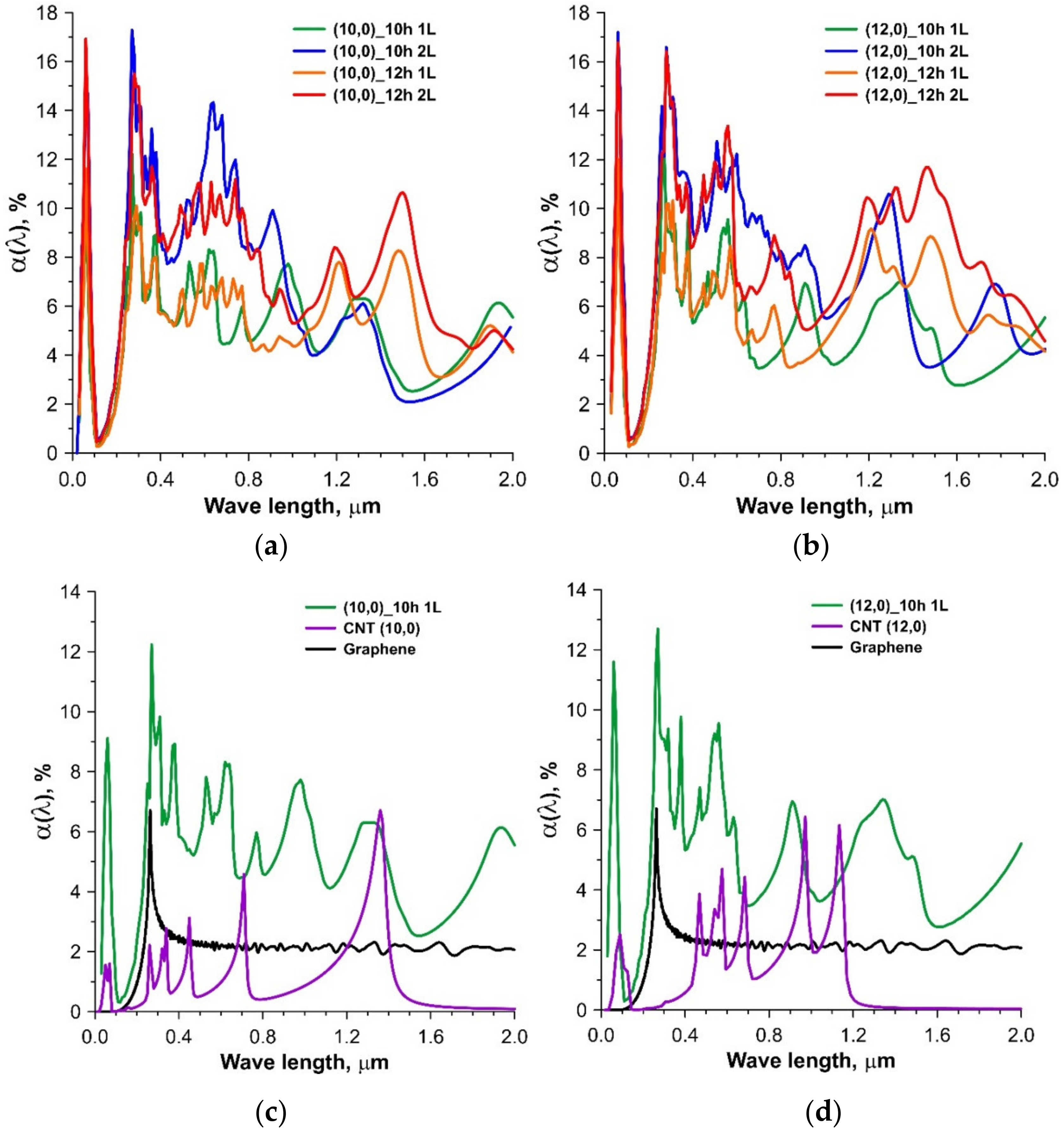
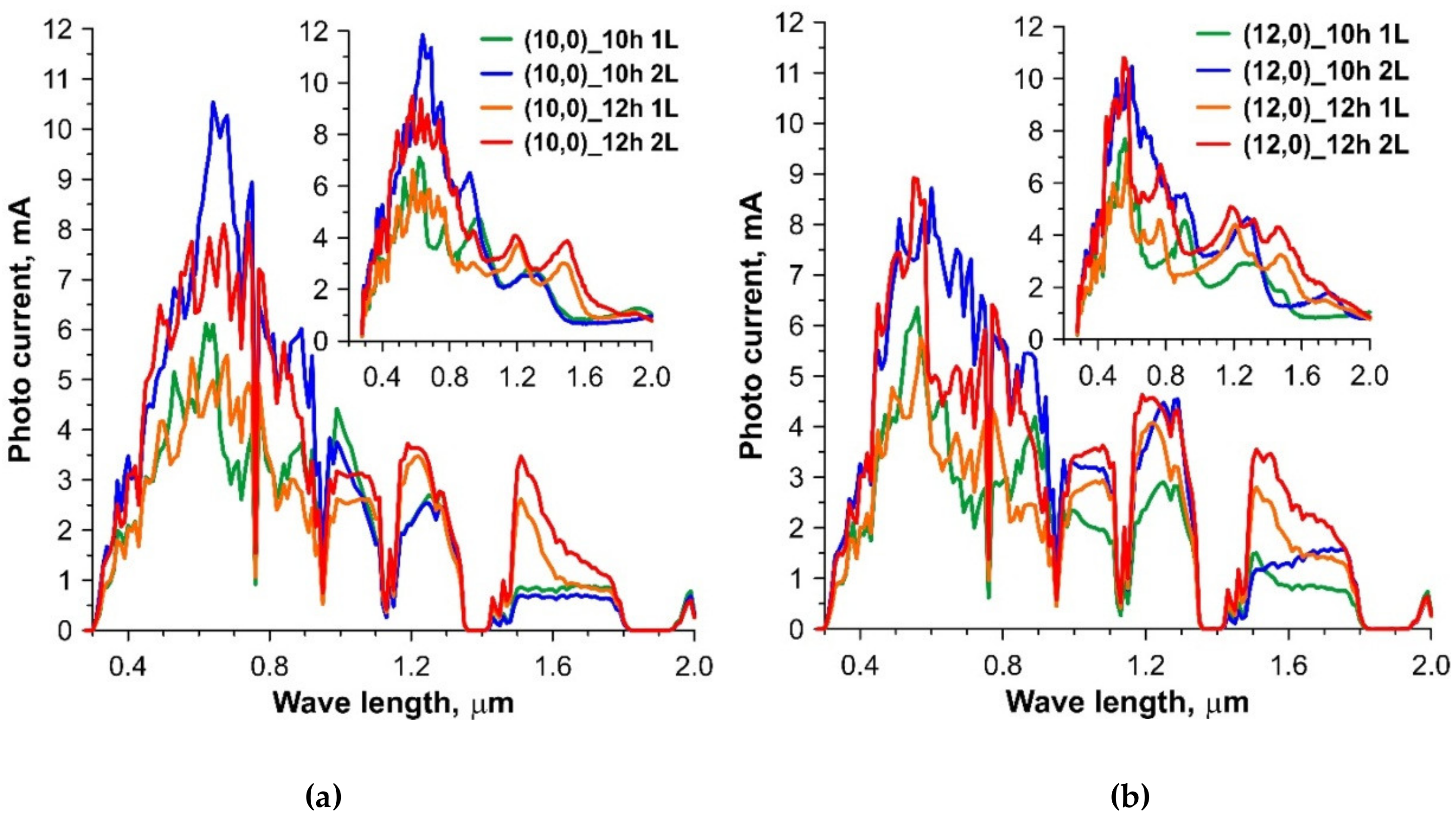
4. Photovoltaic Properties of Layered Graphene/CNT Composite Films

We studied the photovoltaic properties based on the analysis of the profile of the spectra of the maximum photocurrent in the wavelength range λ from 280 to 2000 nm (with a step of 10 nm). The integral values of the maximum photocurrent were also calculated. The maximum photocurrent value for a given frequency ω is calculated by the equation
I max ( ω ) = e P i n ω α ( ω ) ,
where Pin is the power of the incident solar radiation, α(ω) is the absorption coefficient. Equation (2) allows us to calculate the maximum photocurrent because it does not take into account the electron-hole partial recombination. It is applicable to the case of an internal quantum yield of 100%, when each absorbed photon generates an electron. However, the spectrum of the maximum photocurrent allows us to assess the potential possibilities of using this composite for photovoltaics. The absorption coefficient is determined by the well-known equation
α ( ω ) = 1 R ( ω ) 2 T ( ω ) 2 ,
where R(ω) is the reflection coefficient, and T(ω) is the transmittance coefficient. The R(ω) and T(ω) coefficients are calculated using the optical conductivity tensor σαβ(ω) [36]. The optical conductivity tensor σαβ(ω) was calculated using the Kubo–Greenwood formula [37].
The calculated absorption spectra in the range of 20–2000 nm for the monolayer (1L) and bilayer (2L) graphene/CNT composite films with CNTs (10,0) are shown in Figure 4a, and with CNTs (12,0) in Figure 4b. Also, for an effective analysis of the relief of the spectra, the absorption spectra of a graphene monolayer (black curve) and the individual CNTs (10,0) and (12,0) (purple curves) were calculated. These spectra are shown in Figure 4c,d. An analysis of the relief of the spectra shows that a peak at a wavelength of 265 nm is characteristic of all the topological variants of graphene/CNT composite film. This peak is also observed in the spectrum of a graphene monolayer. Another intense peak at a wavelength of 60 nm is explained by the peak in the spectra of the individual CNTs (10,0) and (12,0), as seen in Figure 4c,d. The presence of the numerous peaks in the visible region for the mono- and bilayer graphene/CNT composite films is explained by the peaks in the spectra of the individual nanotubes of this wavelength range. An interesting phenomenon is the appearance of a clear peak at a wavelength of 1500 nm in the spectra of the mono- and bilayer graphene/CNT composite films with a distance between the adjacent nanotubes of 12 hexagons. Moreover, the presence of these peaks is typical for graphene/CNT composite films with CNTs (10,0) and CNTs (12,0). These peaks are shown in Figure 4a,b by the red and orange curves. Their appearance at this wavelength cannot be explained by the spectra of the individual CNTs. Therefore, it can be argued that they are caused by the presence of sp3-hybridized electron clouds, which provide a covalent bond between the CNTs and graphene layers. The phenomenon of sp3-hybridization also explains the appearance of the additional peaks in the near-infrared range (IR), as well as in the visible region.
Based on the data of the absorption spectra and solar radiation spectra, the photocurrent spectra were calculated. The spectrum of solar radiation outside the Earth’s atmosphere, AM0, and the spectrum at the Earth’s surface, AM1.5, were taken from the National Renewable Energy Laboratory (NREL) website [38], where solar spectra are presented in the wavelength range of 280–2000 nm. The photocurrent spectra of the monolayer (1L) and bilayer (2L) graphene/CNT composite films at AM1.5 are shown in Figure 5. The photocurrent spectra at AM0 are presented in the insets in Figure 5. The photocurrent values are given for a surface area of 1 cm2. From the data in Figure 5, it can be seen that, with a change in the diameter of the nanotubes, the spectral peaks shift slightly and, with a change in the distance between the nanotubes, the peak intensity changes. Among all the considered models of graphene/CNT composite films, the highest photocurrent value is observed at a wavelength of 650 nm for a bilayer film with CNTs (10,0) at a distance of 10 hexagons, i.e., in the case of the densest packing of the nanotubes. This photocurrent value is ~ 10.5 mA at the Earth’s surface and ~ 12 mA outside the Earth’s atmosphere. As is the case for the absorption spectra, the photocurrent spectrum also exhibits characteristic peaks in the IR range at a wavelength of 1500 nm.
One of the most important physical characteristics of solar cells and other photovoltaic devices is the magnitude of the integrated photocurrent. It is calculated as the integral of the photocurrent spectrum. Table 3 shows the integrated photocurrent values calculated for the wavelength range of 280–2000 nm for all the considered atomistic models of graphene/CNT composite films with different distances between the nanotubes. It can be seen that as the distance between the nanotubes increases, the photocurrent increases slightly. However, it is impossible to judge the effect of distance from two cases. Therefore, we conducted additional studies for the monolayer films, where the distance between the nanotubes could vary in increments of one hexagon. For the bilayer films, the distance between the nanotubes should be a multiple of two, as shown above. According to the results of an additional study, it was found that there is no obvious dependence of the integrated photocurrent on the distance between the nanotubes, and the photocurrent varies between 3%–4%. As shown in Table 3, the highest photocurrent values are inherent in graphene/CNT composite films with a distance of 12 hexagons between the nanotubes. This is due to the presence of high-intensity peaks in the IR range, as noted above.

5. Conclusions

Some of the physical parameters of mono- and bilayer composite graphene/CNT composite films were determined to identify the prospects for their use in electronics and photovoltaics. Composite films with the CNTs (10,0) and (12,0), regularly located relative to each other at different distances, were studied. In all cases, the nanotubes were covalently bonded to the graphene layers. All types of the composite films exhibit semiconductor properties with an energy gap of 0.47–0.54 eV, which is an important condition for creating solar cell elements based on these composite films. Based on the calculated families of the current–voltage characteristics, we can conclude that, at a voltage of 2 V, the electric current reaches ~ 50 μA for the monolayer films and ~ 90 μA for the bilayer films. Therefore, the distance between the adjacent nanotubes affects the magnitude of the current. This fact indicates the possibility of having topological control of the electrophysical properties of the considered composite films.
Based on the results of the studies of the photovoltaic and optical properties of graphene/CNT composite films, it can be concluded that control of the diameter of the nanotubes and the distance between them allows us to control the profile of the absorption spectrum of the electromagnetic waves in the range of 20–2000 nm. In particular, a change in the diameter of the CNT leads to a shift in the peaks of maximum intensity. The control of the distance between SWCNTs allows one to control the absorption intensity without a significant peak shift. The calculated characteristics show that graphene/CNT composite films are a very effective material for generating a photocurrent. The values of the integrated photocurrent (outside the Earth’s atmosphere) are ~ 22% higher than those of some of the best materials for generating a photocurrent, namely transition metal dichalcogenides MoS2 (3.9 mA/cm2), MoSe2 (4.6mA/cm2) and WS2 (2.3mA/cm2) [39]. These conclusions relate to all the considered graphene/CNT composite films, almost independently of the diameter of the nanotubes and the distance between them, which is extremely important from the point of view of their application in photovoltaics and optoelectronics.

Author Contributions

Conceptualization, O.E.G.; Methodology, O.E.G. and I.S.N.; Funding acquisition, O.E.G., V.V.M., M.M.S.; Investigation, O.E.G., I.S.N., V.V.M., M.M.S.; Writing—Original Draft Preparation, V.V.M. and M.M.S.; Writing—Review and Editing, I.S.N. and O.E.G.; Supervision, O.E.G. All authors have read and agreed to the published version of the manuscript.

Funding

This study was supported by the Ministry of Science and Higher Education of the Russian Federation in the framework of the government task (project No. FSRR-2020-0004).

Conflicts of Interest

The authors declare no conflict of interest.

References

  1. Kim, H.; Kim, J.; Jeong, H.S.; Kim, H.; Lee, H.; Ha, J.M.; Choi, S.M.; Kim, T.H.; Nah, Y.C.; Shin, T.J.; et al. Spontaneous hybrids of graphene and carbon nanotube arrays at the liquid-gas interface for Li-ion battery anodes. Chem Commun. 2018, 54, 5229–5232. [Google Scholar] [CrossRef] [PubMed]
  2. Biswas, C.; Lee, Y.H. Graphene versus carbon nanotubes in electronic devices. Adv. Funct. Mater. 2011, 21, 3806–3826. [Google Scholar] [CrossRef]
  3. Nardecchia, S.; Carriazo, D.; Ferrer, M.L.; Gutiérreza, M.C.; del Monte, F. Three dimensional macroporous architectures and aerogels built of carbon nanotubes and/or graphene: Synthesis and applications. Chem. Soc. Rev. 2013, 42, 794–830. [Google Scholar] [CrossRef] [PubMed]
  4. Moghadam, A.D.; Omrani, E.; Menezes, P.L.; Rohatgi, P.K. Mechanical and tribological properties of self-lubricating metal matrix nanocomposites reinforced by carbon nanotubes (CNTs) and graphene—A review. Compos. B Eng. 2015, 77, 402–420. [Google Scholar] [CrossRef]
  5. Xia, K.; Zhan, H.; Gu, Y. Graphene and Carbon Nanotube Hybrid Structure: A Review. Procedia IUTAM 2017, 21, 94–101. [Google Scholar] [CrossRef]
  6. Prajapati, A.K.; Omrani, E.; Menezes, P.L.; Rohatgi, P.K. Fundamentals of Solid Lubricants. In Self-Lubricating Composites, 1st ed.; Menezes, P., Rohatgi, P., Omrani, E., Eds.; Springer: Berlin, Germany, 2018; Chapter 1; pp. 292–325. ISBN 978-3-662-56527-8. [Google Scholar]
  7. Dang, V.T.; Nguyen, D.D.; Cao, T.T.; Le, P.H.; Tran, D.L.; Phan, N.M.; Nguyen, V.C. Recent trends in preparation and application of carbon nanotube–graphene hybrid thin films. Adv. Nat. Sci. Nanosci. Nanotechnol. 2016, 7, 033002. [Google Scholar] [CrossRef] [Green Version]
  8. Tristán-López, F.; Morelos-Gómez, A.; Vega-Díaz, S.M.; García-Betancourt, M.L.; Perea-López, N.; Elías, A.L.; Muramatsu, H.; Cruz-Silva, R.; Tsuruoka, S.; Kim, Y.A.; et al. Large Area Films of Alternating Graphene–Carbon Nanotube Layers Processed in Water. ACS Nano 2013, 7, 10788–10798. [Google Scholar]
  9. Lv, R.; Cruz-Silva, E.; Terrones, M. Building Complex Hybrid Carbon Architectures by Covalent Interconnections: Graphene–Nanotube Hybrids and More. ACS Nano 2014, 8, 4061–4069. [Google Scholar] [CrossRef]
  10. Kim, S.H.; Song, W.; Jung, M.W.; Kang, M.A.; Kim, K.; Chang, S.J.; Lee, S.S.; Lim, J.; Hwang, J.; Myung, S.; et al. Carbon Nanotube and Graphene Hybrid Thin Film for Transparent Electrodes and Field Effect Transistors. Adv. Mater. 2014, 26, 4247–4252. [Google Scholar] [CrossRef]
  11. Gan, X.; Lv, R.; Bai, J.; Zhang, Z.; Wei, J.; Huang, Z.H.; Zhu, H.; Kang, F.; Terrones, M. Efficient photovoltaic conversion of graphene–carbon nanotube hybrid films grown from solid precursors. 2D Mater. 2015, 2, 034003. [Google Scholar] [CrossRef]
  12. Kholmanov, I.N.; Magnuson, C.W.; Piner, R.; Kim, J.Y.; Aliev, A.E.; Tan, C.; Kim, T.Y.; Zakhidov, A.A.; Sberveglieri, G.; Baughman, R.H.; et al. Optical, electrical, and electromechanical properties of hybrid graphene/carbon nanotube films. Adv. Mater. 2015, 27, 3053–3059. [Google Scholar] [CrossRef] [PubMed]
  13. Yan, Z.; Peng, Z.; Casillas, G.; Lin, J.; Xiang, C.; Zhou, H.; Yang, Y.; Ruan, G.; Raji, A.R.O.; Samuel, E.L.G.; et al. Rebar Graphene. ACS Nano 2014, 8, 5061–5068. [Google Scholar] [CrossRef] [PubMed]
  14. Chuc, N.V.; Thanh, C.T.; Tu, N.V.; Phuong, V.T.Q.; Thang, P.V.; Tam, N.T.T. A Simple Approach to the Fabrication of Graphene-Carbon Nanotube Hybrid Films on Copper Substrate by Chemical Vapor Deposition. J. Mater. Sci. Technol. 2015, 31, 479–483. [Google Scholar] [CrossRef]
  15. Li, L.; Li, H.; Guo, Y.; Yang, L.; Fang, Y. Direct synthesis of graphene/carbon nanotube hybrid films from multiwalled carbon nanotubes on copper. Carbon 2017, 118, 675–679. [Google Scholar] [CrossRef]
  16. Zhang, J.; Chen, Z.; Xu, X.; Liao, W.; Yang, L. A simple and efficient approach to fabricate graphene/CNT hybrid transparent conductive films. RSC Adv. 2017, 7, 52555–52560. [Google Scholar] [CrossRef] [Green Version]
  17. Lin, X.; Liu, P.; Wei, Y.; Li, Q.; Wang, J.; Wu, Y.; Feng, C.; Zhang, L.; Fan, S.; Jiang, K. Development of an ultra-thin film comprised of a graphene membrane and carbon nanotube vein support. Nat. Commun. 2013, 4, 2920. [Google Scholar] [CrossRef]
  18. Liu, Y.; Wang, F.; Wang, X.; Wang, X.; Flahaut, E.; Liu, X.; Li, Y.; Wang, X.; Xu, Y.; Shi, Y.; et al. Planar carbon nanotube–graphene hybrid films for high-performance broadband photodetectors. Nat. Commun. 2015, 6, 8589. [Google Scholar] [CrossRef] [Green Version]
  19. Shi, J.; Li, X.; Cheng, H.; Liu, Z.; Zhao, L.; Yang, T.; Dai, Z.; Cheng, Z.; Shi, E.; Yang, L.; et al. Graphene Reinforced Carbon Nanotube Networks for Wearable Strain Sensors. Adv. Funct. Mater. 2016, 26, 2078–2084. [Google Scholar] [CrossRef]
  20. Kim, Y.K.; Min, D.H. Durable Large-Area Thin Films of Graphene/Carbon Nanotube Double Layers as a Transparent Electrode. Langmuir 2009, 25, 11302–11306. [Google Scholar] [CrossRef]
  21. Dong, X.; Li, B.; Wei, A.; Cao, X.; Chan-Park, M.B.; Zhang, H.; Li, L.J.; Huang, W.; Chen, P. One-step growth of graphene–carbon nanotube hybrid materials by chemical vapor deposition. Carbon 2011, 49, 2944–2949. [Google Scholar] [CrossRef]
  22. Nguyen, D.D.; Tai, N.H.; Chena, S.Y.; Chueh, Y.L. Controlled growth of carbon nanotube–graphene hybrid materials for flexible and transparent conductors and electron field emitters. Nanoscale 2012, 4, 632–638. [Google Scholar] [CrossRef] [PubMed]
  23. Nguyen, D.D.; Tiwari, R.N.; Matsuoka, Y.; Hashimoto, G.; Rokuta, E.; Chen, Y.Z.; Chueh, Y.L.; Yoshimura, M. Low vacuum annealing of cellulose acetate on nickel towards transparent conductive CNT-graphene hybrid films. ACS Appl. Mater. Interfaces 2014, 6, 9071–90777. [Google Scholar] [CrossRef] [PubMed]
  24. Hong, T.K.; Lee, D.W.; Choi, H.J.; Shin, H.S.; Kim, B.S. Transparent, flexible conducting hybrid multilayer thin films of multiwalled carbon nanotubes with graphene nanosheets. ACS Nano 2010, 4, 3861–3868. [Google Scholar] [CrossRef] [PubMed]
  25. Maarouf, A.A.; Kasry, A.; Chandra, B.; Martyna, G.J. A graphene–carbon nanotube hybrid material for photovoltaic applications. Carbon 2016, 102, 74–80. [Google Scholar] [CrossRef] [Green Version]
  26. Liu, Y.; Liu, Y.; Qin, S.; Xu, Y.; Zhang, R.; Wang, F. Graphene-carbon nanotube hybrid films for high-performance flexible photodetectors. Nano Res. 2017, 10, 1880–1887. [Google Scholar] [CrossRef]
  27. Cui, X.; Lv, R.; Sagar, R.U.R.; Liu, C.; Zhang, Z. Reduced graphene oxide/carbon nanotube hybrid film as high performance negative electrode for supercapacitor. Electrochim. Acta 2015, 169, 342–350. [Google Scholar] [CrossRef]
  28. Cheng, Q.; Tang, J.; Shinya, N.; Qin, L.C. Co(OH)2 nanosheet-decorated graphene-CNT composite for supercapacitors of high energy density. Sci. Technol. Adv. Mater. 2014, 15, 014206. [Google Scholar] [CrossRef]
  29. Mitrofanov, V.V.; Slepchenkov, M.M.; Zhang, G.; Glukhova, O.E. Hybrid carbon nanotube-graphene monolayer films: Regularities of structure, electronic and optical properties. Carbon 2017, 115, 803–810. [Google Scholar] [CrossRef]
  30. Slepchenkov, M.M.; Glukhova, O.E. Mechanical and Electroconductive Properties of Mono- and Bilayer Graphene–Carbon Nanotube Films. Coatings 2019, 9, 74. [Google Scholar] [CrossRef] [Green Version]
  31. Stuart, S.J.; Tutein, A.B.; Harrison, J.A. A reactive potential for hydrocarbons with intermolecular interactions. J. Chem. Phys. 2000, 112, 6472–6486. [Google Scholar] [CrossRef] [Green Version]
  32. Elstner, M.; Seifert, G. Density functional tight binding. Phil. Trans. R. Soc. A 2014, 372, 20120483. [Google Scholar] [CrossRef] [PubMed] [Green Version]
  33. Glukhova, O.E. Molecular Dynamics as the Tool for Investigation of Carbon Nanostructures Properties. In Thermal Transport in Carbon-Based Nanomaterials, 1st ed.; Zhang, G., Ed.; Elsevier: Oxford, UK, 2017; pp. 267–289. [Google Scholar]
  34. Aradi, B.; Hourahine, B.; Frauenheim, T. DFTB+, a sparse matrix-based implementation of the DFTB method. J. Phys. Chem. A 2007, 111, 5678–5684. [Google Scholar] [CrossRef] [PubMed]
  35. Datta, S. Quantum Transport: Atom to Transistor, 2nd ed.; Cambridge University Press: New York, NY, USA, 2005; pp. 217–251. [Google Scholar]
  36. Glukhova, O.E.; Nefedov, I.S.; Shalin, A.S.; Slepchenkov, M.M. New 2D graphene hybrid composites as an effective base element of optical nanodevices. Beilstein J. Nanotechnol. 2018, 9, 1321–1327. [Google Scholar] [CrossRef] [Green Version]
  37. Calderín, L.; Karasiev, V.V.; Trickey, S.B. Kubo-Greenwood electrical conductivity formulation and implementation for projector augmented wave datasets. Comput. Phys. Commun. 2017, 221, 118–142. [Google Scholar] [CrossRef] [Green Version]
  38. National Renewable Energy Laboratory (NREL). Available online: https://www.nrel.gov/ (accessed on 15 January 2020).
  39. Bernardi, M.; Palummo, M.; Grossman, J. Extraordinary Sunlight Absorption and One Nanometer Thick Photovoltaics Using Two-Dimensional Monolayer Materials. Nano Lett. 2013, 13, 3664–3670. [Google Scholar] [CrossRef]
Figure 1. Atomistic structure of mono- and bilayer graphene/carbon nanotubes (CNT) composite films: (a) super-cells; (b) the general view of the monolayer; (c) general view of the bilayer.
Coatings 10 00324 g001aCoatings 10 00324 g001b
Figure 2. Density of electronic states (DOS) distribution of graphene/CNT composite films with nanotubes (10,0) and (12,0) at distances between adjacent CNTs of 10 and 12 hexagons: (a) monolayer; (b) bilayer.
Coatings 10 00324 g002
Figure 3. Families of current–voltage characteristics of graphene/CNT composite films: (a) monolayer films; (b) bilayer films.
Coatings 10 00324 g003
Figure 4. Absorption spectra of monolayer (1L) and bilayer (2L) graphene/CNT composite films: (a) composite films with CNTs (10,0); (b) composite films with CNTs (12,0); (c) individual CNT (10,0) and graphene, composite films with CNTs (10,0); (d) individual CNT (12,0) and graphene, composite films with CNTs (12,0).
Coatings 10 00324 g004
Figure 5. Photocurrent spectra of monolayer (1L) and bilayer (2L) graphene/CNT composite films at AM1.5: (a) with CNTs (10,0); (b) with CNTs (12,0). The insets show the photocurrent spectra at AM0.
Coatings 10 00324 g005
Table 1. Geometrical characteristics of super-cells of mono- and bilayer graphene/CNT films.
ParametersMonolayer FilmBilayer Film
(10,0)(12,0)(10,0)(12,0)
10 hexagons
Lx, Å24.57024.30024.00024.630
Ly, Å4.2304.2704.2804.290
rt-t, Å18.31416.92017.78417.131
a/b1.6411.6621.6601.654
12 hexagons
Lx, Å29.43029.40028.92029.200
Ly, Å4.3004.3004.2904.290
rt-t, Å23.18721.70222.70621.726
a/b1.6401.6621.6601.655
Table 2. Electron and energy characteristics of mono- and bilayer graphene/CNT composite films.
ParametersMonolayer FilmBilayer Film
(10,0)(12,0)(10,0)(12,0)
10 hexagons
EF, eV−4.66−4.68−4.67−4.69
Egap, eV0.580.470.540.49
12 hexagons
EF, eV−4.68−4.68−4.69−4.68
Egap, eV0.590.540.570.53
Table 3. Integrated photocurrent values of mono- and bilayer graphene/CNT composite films.
ParametersMonolayer FilmBilayer Film
(10,0)(12,0)(10,0)(12,0)
10 hexagons
Photocurrent at AM1.5, mA·cm-23.324.914.715.04
Photocurrent at AM0, mA·cm-24.564.386.216.70
12 hexagons
Photocurrent at AM1.5, mA·cm-23.403.534.915.05
Photocurrent at AM0, mA·cm-24.714.936.677.00

