Effects of Laser Fluence and Pulse Overlap on Machining of Microchannels in Alumina Ceramics Using an Nd:YAG Laser


1
Advanced Manufacturing Institute, King Saud University, P.O. Box 800, Riyadh 11421, Saudi Arabia
2
Industrial Engineering Department, College of Engineering, King Saud University, P.O. Box 800, Riyadh 11421, Saudi Arabia
*
Author to whom correspondence should be addressed.
Appl. Sci. 2019, 9(19), 3962; https://doi.org/10.3390/app9193962
Submission received: 5 August 2019
/
Revised: 5 September 2019
/
Accepted: 17 September 2019
/
Published: 20 September 2019
(This article belongs to the Special Issue Microfluidics in Biomedical Engineering)
Abstract
:The quality of micro-features in various technologies is mostly affected by the choice of the micro-fabrication technique, which in turn results in several limitations with regard to materials, productivity, and cost. Laser beam micro-machining has a distinct edge over other non-traditional methods in terms of material choices, precision, shape complexity, and surface integrity. This study investigates the effect of laser fluence and pulse overlap while developing microchannels in alumina ceramic using an neodymium-doped yttrium aluminum garnet (Nd:YAG) laser. Microchannels 200 µm wide with different depths were machined using different laser peak fluence and pulse overlap (percentage of overlap between successive laser pulses) values. It was found that high pulse overlaps and fluences should be avoided as they give rise to V-shaped microchannels i.e., 100% bottom width errors. The optimal peak fluence range was found to be around 125–130 J/cm2 corresponding to 3–5 µm depth per scan. In addition, channels fabricated with moderate pulse overlap were found to be of good quality compared to low pulse overlaps.
1. Introduction
Structural ceramics find many applications in microfeature products due to their exceptional properties such as wear resistant, chemical inertness, high temperature strength, and dimensional stability. One of the most important and readily available structural ceramic is Alumina. Alumina micro-featured products have applications in many areas like microelectronics due to their excellent dielectric strength and in microreactors as heat and corrosive-resistant material with low thermal expansion. Similarly, they are being utilized for many wear resistance applications like parts in micro- pumps, valves, and thread/wire guides.
Conventional processing methods to fabricate micro features in structural ceramics are not able to meet the designed requirements in various areas like micro-electronics, bio-medical applications and microreactors etc. The microfeatures in these applications require high dimensional accuracy with very fine surface finish. In addition, absence of microcracks, residual stresses, and heat affected zones is crucial to ensure smart product architecture resulting in high performance integration [1,2].
Traditionally structural ceramics are processed using techniques similar to powder metallurgy. However, manufacturing of high precision and defect free ceramic micro parts using these methods poses significant challenges in terms of tool development and raw material preparation. Good quality ceramic parts require high precision molds and very fine powder preparation. These constraints restrict the technology to high volume production and thus are not suitable for applications requiring customized parts and shorter product development times. Other processing methods like electrochemical deposition and photolithography are also being investigated for ceramic micro features. However, these methods are not easy to implement, involve chemical handling, and are associated with long processing times [3,4].
Additive manufacturing methods which have been primarily developed for polymeric materials are also being adapted to manufacture metallic and ceramic micro parts. These methods do not require any mold preparation and processing is computer controlled. However, the quality of the micro parts is not comparable to other methods in terms of porosity, residual stresses, and surface finish [5].
Micro-machining through mechanical cutting is the most prevalent method to fabricate micro parts. With precision machine tools, it is possible to produce good surface finish and form accuracy. However, at the same time, these tool contact-based methods are subjected to excessive tool wear and micro-cracks especially for ceramic micro parts. In contrast non-conventional machining methods like micro-electric-discharge machining (Micro-EDM), micro-ultrasonic machining (Micro-USM), and micro-laser-beam machining (Micro-LBM) are able to produce extremely fine accuracy and better surface integrity with little or no tool wear. Specifically, Micro-LBM is an excellent choice for machining ceramic parts as it provides better process control, improved dimensional accuracy, and easier set-up in comparison to other methods [6].
Microprocessing of ceramics using an Nd:YAG or excimer laser has been investigated by many researchers using pulse widths in milli-, micro-, nano-, and pico-second range while generating different microstructures. Effects of laser intensity/fluence, wavelength, scan speed, pulse repetition rate, pulse width, and air pressure were investigated on different performance measures like dimensional accuracy, ablation efficiency, heat affected zone, recast layers, surface roughness, and microcracks etc.
Microstructure development in titanium nitrate using femtosecond lasers was carried out by Bonse et al. [7]. They compared circularly polarized radiation with linearly polarized radiation and concluded that the former produces good surface finish and increased ablation rates using the same laser fluence. Chen and Darling [8] utilized a near ultraviolet Nd:YAG laser for micromachining of sapphire and silicon. They found higher ablation efficiency when laser fluence increased slightly above the threshold values. However further increase in fluence did not show any improvement in ablation efficiency possibly due to laser attenuation.
A short pulse Nd:YAG laser having wavelength of 355 nm and pulse duration of 15 ns was utilized by Otani et al. [9] to generate microfeatures in diamond, silicon, and stainless steel. They showed that 1 mm thick silicon wafers can be machined easily without any microcracks but a small increase in pulse width resulted in thermal damage. For diamond, the third harmonic of an Nd:YAG laser was found to be suitable due to high absorption at this wavelength whereas steel was found to be less sensitive to the wavelength and microholes of good quality could be created at 1064, 532, and 355 nm wavelengths. Wernicke et al. [10] produced microholes in Aluminum Gallium Nitride/Gallium Nitride transistors utilizing single crystal silicon carbide as substrate. They concluded that laser micromachining is a better choice in comparison to lithography and dry etching for these hard and chemically inert materials.
Super hard nano polycrystalline diamond was machined by Okuchi et al. [11] using three types of lasers: (a) nanosecond near-ultraviolet, (b) nanosecond near-infrared, (c) femtosecond near-infrared. It was found that rough surfaces were produced by ns laser with high average power. In contrast smooth surfaces were obtained using femtosecond laser with low average power. Mutlu et al. [12] performed micro-drilling on alumina ceramic plate using a second and third harmonic Nd:YAG laser with a 6 ns pulse width. They showed that the plasma shielding mode is dominant at this wavelength and the increase of the diameter is more than the depth with the increase in average power. They also reported a decrease in crater diameter with increase of ambient pressure. A dual prism optical system with a UV Nd:YAG laser was utilized by Pan et al. [13] to make different microfeatures on silicon wafers. They were able to develop microfeatures up to an aspect ratio of 10 that could be used for signal transducing elements in micro-electro-mechanical systems (MEMS). They reported that the efficiency of laser micromachining is not affected by the orientation of the silicon substrate.
Matsuoka [14] examined trepanned drilling of through holes in borosilicate glass using fourth harmonic Nd:YAG laser. They reported an increase in the number of pulses and a decrease in the number of circular scans by increasing the number of lines per circular scans. Microhole drilling in metals, alloys, and ceramics using a picosecond laser was studied by Hu et al. [15]. They utilized laser of wavelengths of 532 nm and 1064 nm with a percussion drilling technique and holes less than 50 µm were produced in steel, silicon nitride and silicon carbide. They concluded that high quality microstructures can be produced in different materials by picosecond lasers.
Microstructures in fused silica were examined by Vukelic et al. [16] and they analyzed different mechanisms at very high laser fluence. According to them the ablation phenomenon is mainly dependent on feedrate while pulse energy mainly accounts for feature size. Analysis of microholes in alumina ceramic using a nanosecond laser was carried out by Li et al. [17] and they reported an improvement in the quality of microholes using laser repeat drilling in static water.
Liu et al. [18] studied the micro-groove development by nanosecond laser in green ZrO2 ceramics. They investigated the effects of power, frequency, and scanning speed on morphology and the heat-affected zone around the machined textured grooves. They suggested power below 6 watts, frequency below 40 Hz, and scanning speed above 60 Hz for good surface quality. Femtosecond laser with helical drilling technique was utilized by Zhang et al. [19] to make blind and through holes in titanium carbide. The quality of holes was analyzed by changing the spiral number, processing time, laser fluence, and repetition rate. The concluded that ablation efficiency and quality is mainly dependent on laser fluence and pulse repetition rate.
Xing et al. [20,21] developed nano-textures in Al2O3/TiC and Si3N4 ceramics using a femtosecond laser. They showed that pulse energy and scanning speed are the dominant factors for the surface morphology and ablation depth and optimum settings were found to be 1.75 μJ with 500 μm/s or 2 μJ with 500 μm/s. Microholes in alumina ceramics were studied by Hanon et al. [22] using a millisecond pulsed laser. They reported that the peak power and pulse duration are the main factors in determining the crater depth for single pulse application.
Li et al. [23] used two different methods with nanosecond laser to develop a micro-surface texture on alumina ceramic. For single pulse interval processing, crater depth and diameter increase with the increase in pulse energy and number of pulses. With the ring cutting processing, the micro- pit depth increases with the average power and the micro-pit diameter is mainly controlled by the scan diameter. Microchannels fabrication in Al2O3/TiC ceramic by a nanosecond laser was analyzed by Xing et al. [24]. The effects of overscans, frequency, scanning speed, and voltage on dimensional accuracy and surface quality were investigated. It was reported that channel width and depth increase with the increase in voltage, frequency, and number of overscans and decrease with the scanning speed.
It is evident from the literature that studies related to microchannel development in alumina ceramic are rare and there is a need to assess the capabilities of Nd:YAG microsecond lasers with respect to dimensional accuracies. In this study the effects of laser fluence and pulse overlap were investigated while developing microchannels using Nd:YAG lasers having a pulse width in the microsecond range. In addition, the current study provides a relationship between laser fluence, pulse overlap, and depth of material removed per laser scan (D/S). The interpretation of relations between process parameters and microchannel quality is significant for the accurate fabrication of microchannels in alumina ceramics. The developed microchannels were analyzed in terms of variations in top width error, bottom width error, depth of material removed per laser scan, and the material removal rate.
2. Material and Method
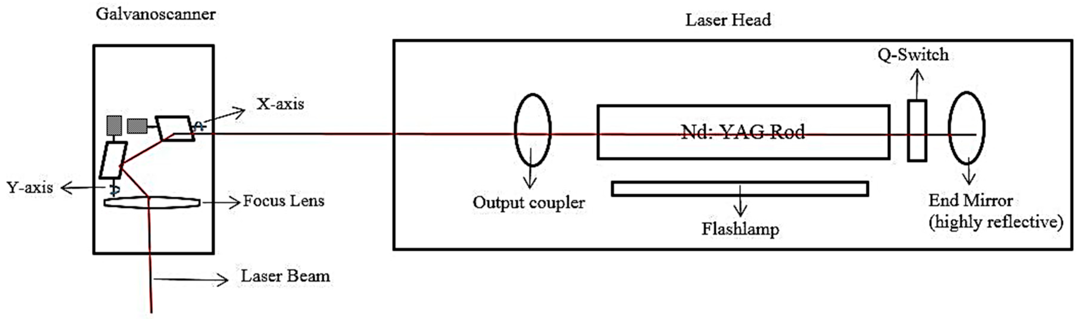
Alumina (Al2O3, 99.7%) samples of dimensions 50 × 50 × 10 mm from Ceram Tec® Germany were used as the workpiece material. The experimental setup used in this work was lasertec-40 from Deckel Maho Gildemeister, Germany. It is equipped with a Flashlamp pumped Nd:YAG laser with a wavelength of 1064 nm and maximum power of 30 W. The laser beam is operated in fundamental Gaussian mode (TEM00) and focused on the workpiece with the help of a galvanoscanner as shown in the schematic in Figure 1. The specifications and laser process parameters used in this study were as shown in Table 1.
Microchannels of dimension 200 µm width and 5 mm length were machined by varying the laser fluence at three different pulse overlaps 58%, 67%, and 75%.
Pulse overlap is the percentage of overlap between successive laser pulses and is given by the following Equation (1).
V is the laser scan speed which was varied at 75, 60, 45 mm/s, f is the pulse frequency and D is the laser spot size which were fixed at 6000 Hz and 0.03 mm respectively based on previous experimental findings.
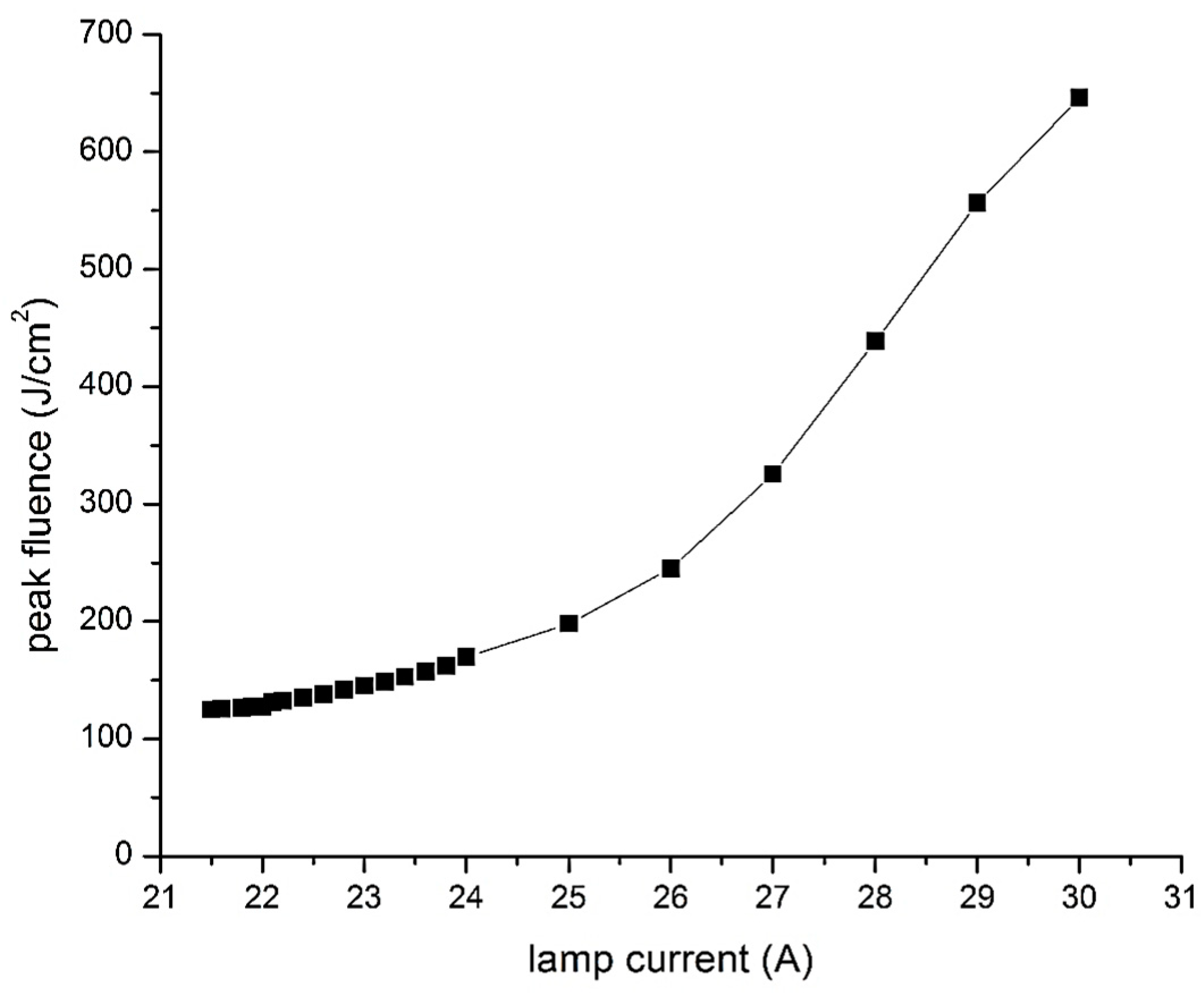
In this study laser fluence was varied by varying the Flashlamp current as shown in Figure 2. A laser power meter (Ophir Nova-II) in combination with a sensor (Ophir L50) was utilized to measure the average power input for each of the lamp intensity settings. Average power and pulse frequency together were used to calculate the laser peak fluence.
Two microchannels were machined at each experimental condition and the averages were utilized for the analysis. Channels were cut through the cross-section using an Isomet® 1000 precision saw from Bueler. The cross-sections were viewed under JEOL JSM-6610LV Scanning Electron Microscope (SEM). The channels were analyzed with respect to material removal rate (MRR) and width error, that is the difference between the actual width and the target width. At the top of the channel, referred to as top width error (TWE), and at the bottom, referred as bottom width error (BWE) and depth per scan (D/S), is the total depth obtained over the number of laser scans. The obtained channels were uniform throughout the 5 mm length. The cross-sections of a few channels were analyzed at three points along the length. The variation within the individual channel measurements was found to be within 1%. The process was found to have good repeatability, the average variation in the width and depth within the repetitions was found to be around 2%, and 3% respectively.
3. Results and Discussions
3.1. Effect of Laser Fluence and Pulse Overlap on Microchannel Geometry
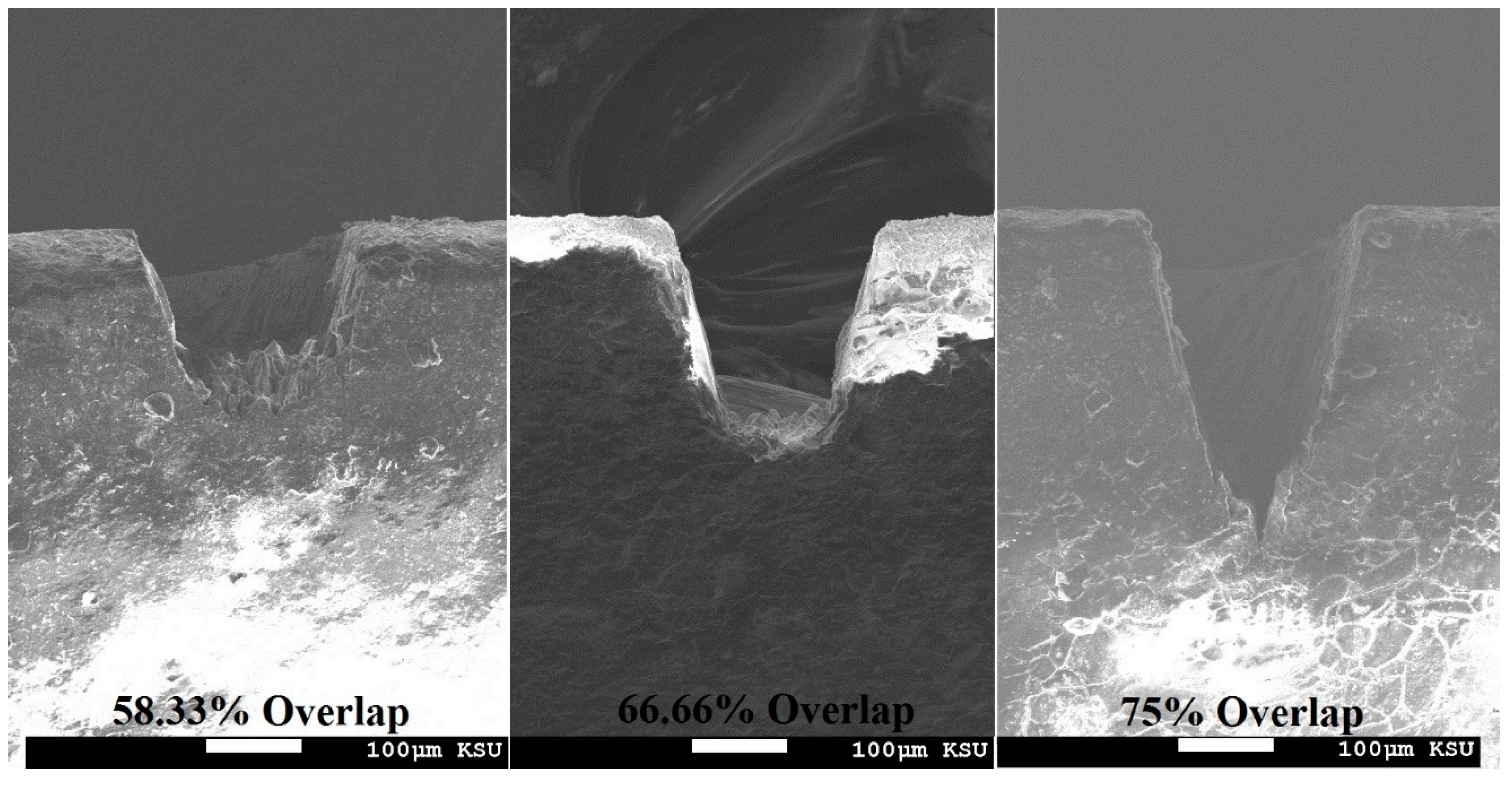
Table 2 shows the design array with the corresponding performance measures of the microchannels fabricated by varying peak fluence and pulse overlap for 24 laser scans. Figure 3 shows the SEM image of the microchannel cross-sections with varying pulse overlap at the peak fluence of 169.76 J/cm2. It was found that both peak fluence and pulse overlap had significant effects on the microchannel geometry. An increase in pulse overlap results in an increase in microchannel size and taper. The microchannels obtained at lower pulse overlaps were less deep and had minimum taper whereas at high pulse overlaps the microchannels were associated with high taper angle resulting in V-shaped channels as shown in Figure 3. In general, medium pulse overlap of 66.66% produced better channels.
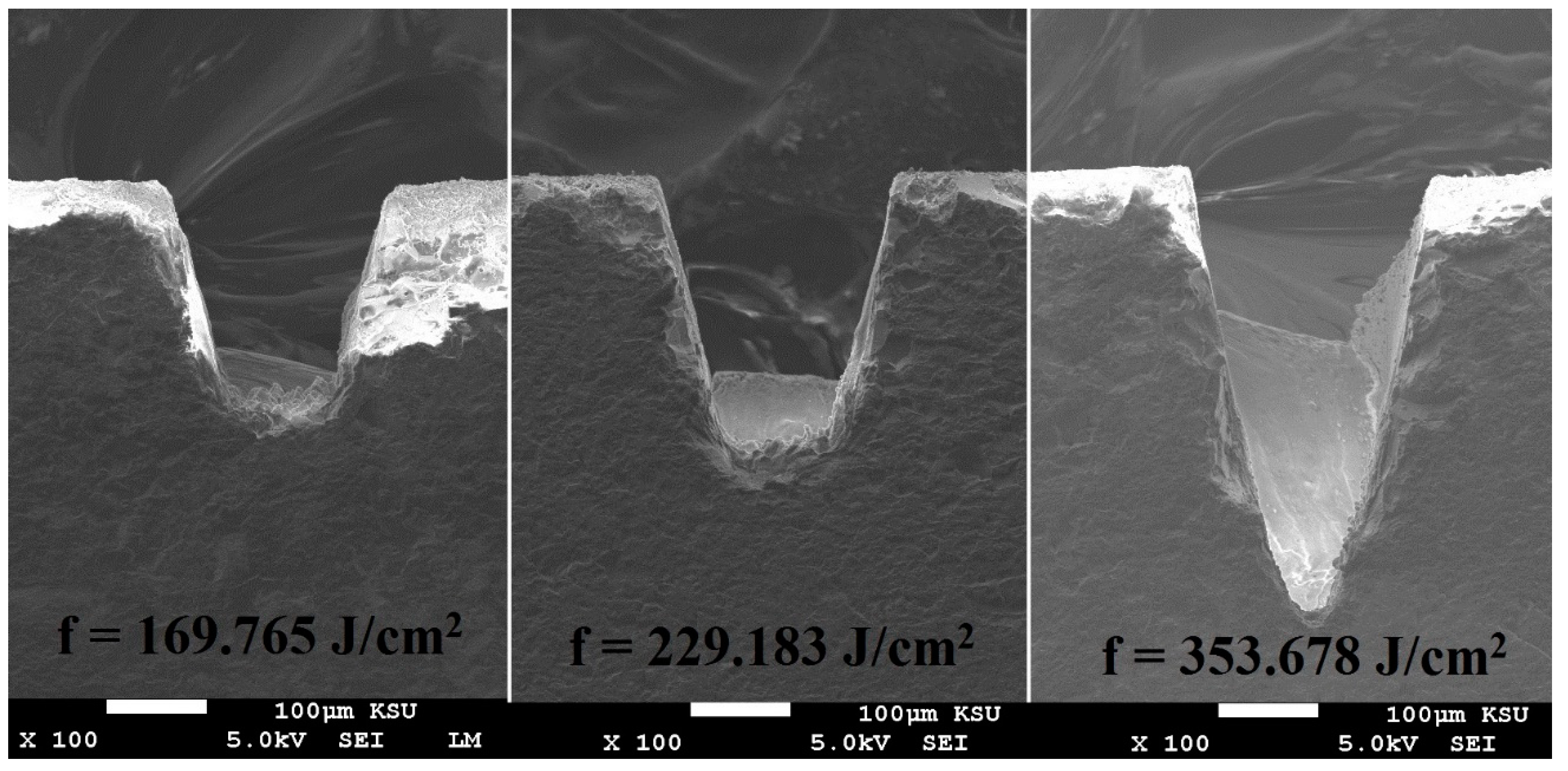
Figure 4 shows the variation of microchannel geometry with increasing peak fluence at a fixed pulse overlap of 66.66%. It can be seen that low and medium peak fluence result in a flat surface at the bottom of the channel whereas higher peak fluence results in V-shaped microchannels.
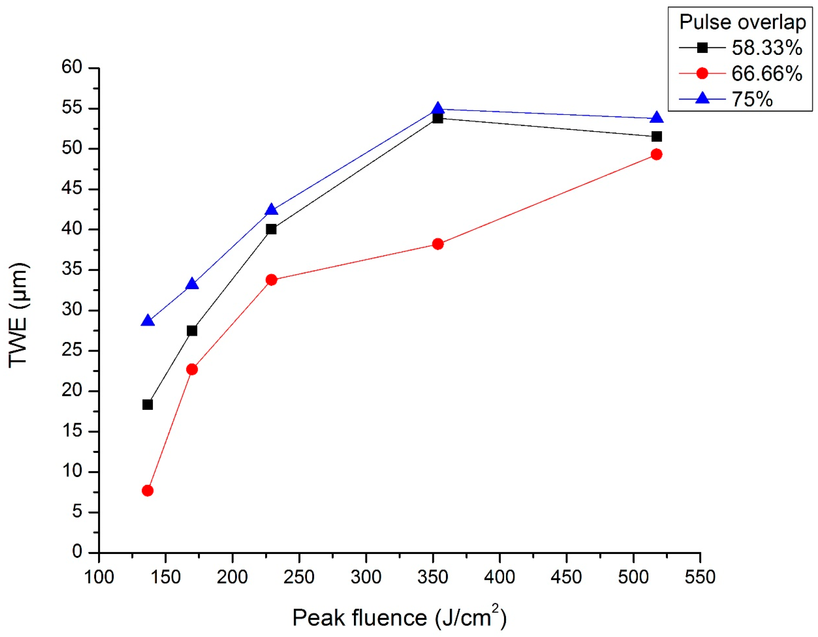
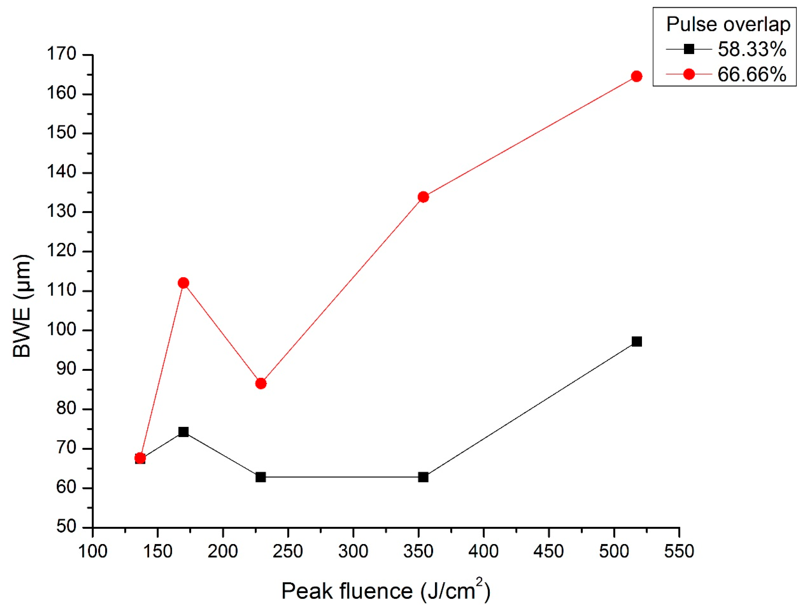
Both the laser peak fluence and pulse overlap have a significant effect on the channel width. The TWE increased with increase in peak fluence and the pulse overlap except for the 66.66% pulse overlap, which resulted in channels with TWE less than the lowest pulse overlap as shown in Figure 5. In general, low fluence and 66.66% pulse overlap resulted in microchannels with width closer to the target width. The increase in TWE with fluence and overlap is because at a higher fluence and overlap the energy density is higher which results in a high volume of molten material. This molten material is ejected out through the cross-section of the channel at high speed and erodes the top edge resulting in a greater width of the microchannel. Figure 6 shows the effect of peak fluence and pulse overlap on the bottom width of the channel. BWE increases with increase in peak fluence and pulse overlap. At low peak fluence, the difference in BWE for both the pulse overlaps of 58.33% and 66.66% is minimum; however, this difference increases significantly with the increase in peak fluence. This is because at higher fluence levels, the depth of material removed is higher and as the depth increases, it makes the ejection of molten material difficult from the channel resulting in taper and lower bottom width. The pulse overlap of 75% resulted in V-shaped microchannels. This is because at higher overlap, the energy density is higher which results in a high volume of molten material and a high depth of cut. Moreover, once the molten metal has adhered to the wall of the channel, the laser loses the focus for the subsequent layers resulting in a V-shaped channel.
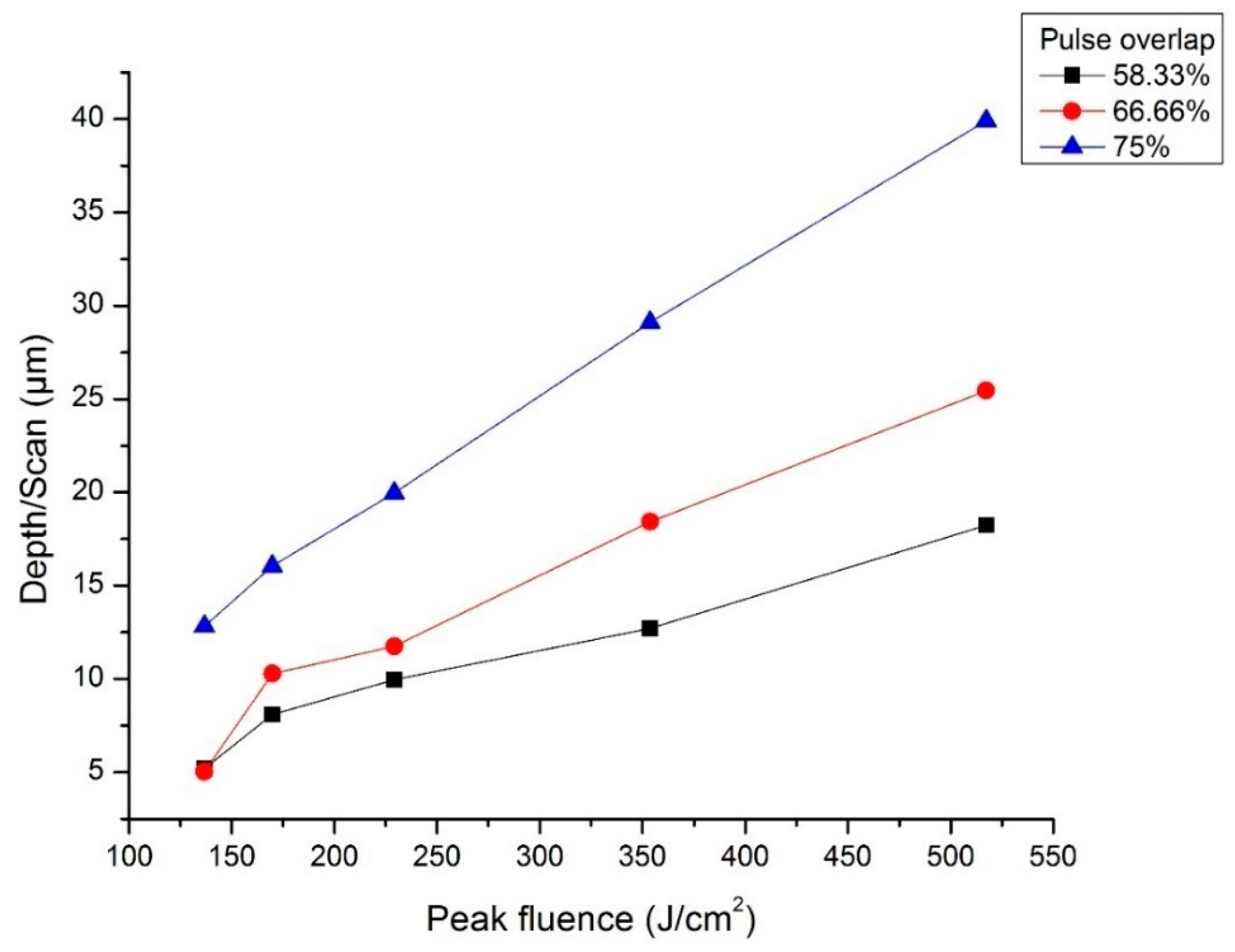
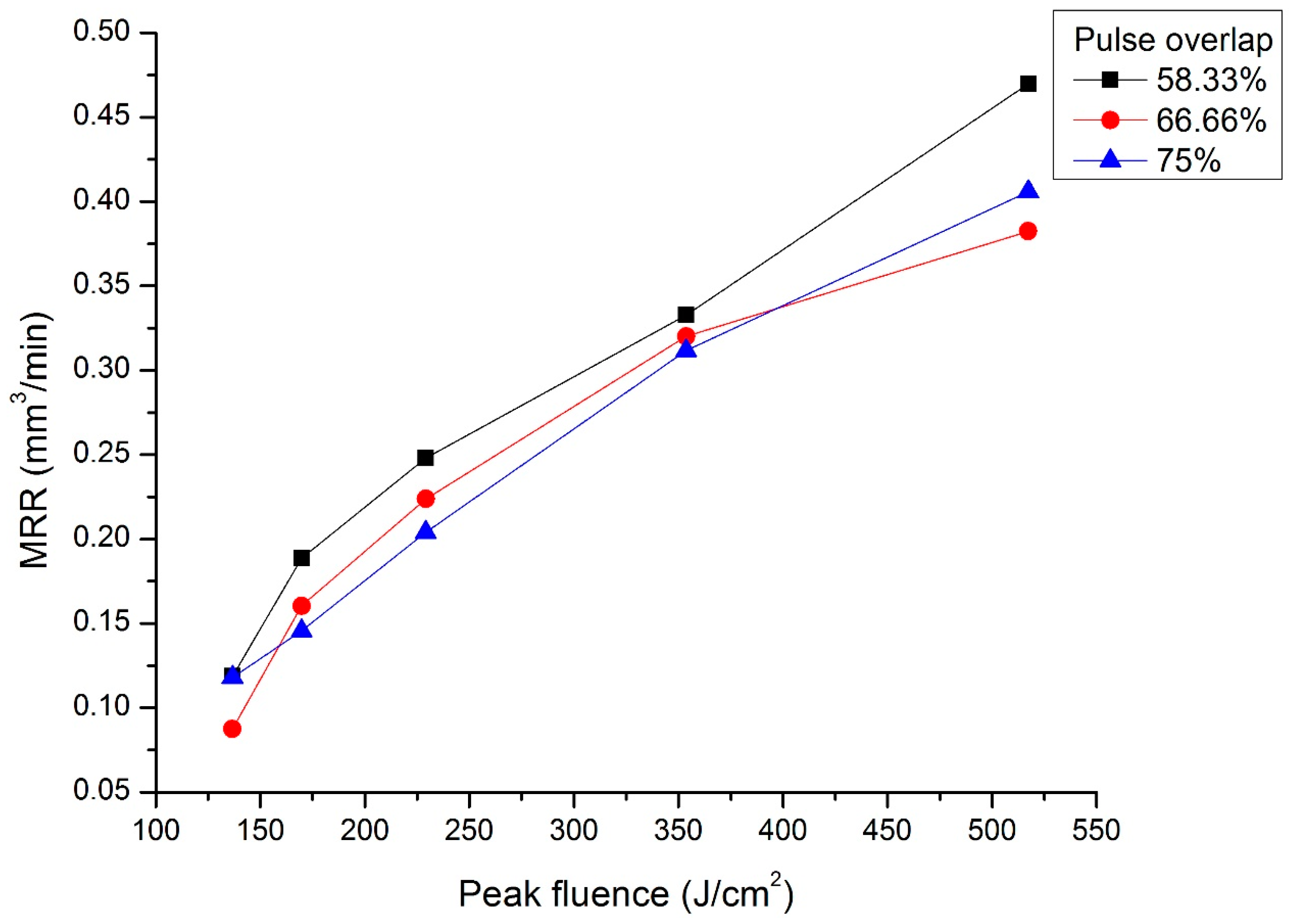
As expected, the channel depth increases with increase in peak fluence and pulse overlap. Increase in fluence and pulse overlap increases the energy density and laser penetration into the material, which results in a higher depth of material being removed for each laser scan, thereby producing a channel with higher depth. Figure 7 shows the effect of peak fluence and pulse overlap on the depth per scan. It can be seen that at lower fluence, the difference in depth is minimum for different pulse overlaps. However, this difference increases significantly as the fluence increases, because at higher fluence energy the density is higher which in conjunction with the overlap increases the depth of material removed. Figure 8 shows the variation of MRR with peak fluence and pulse overlap. In general, it was found that in the selected pulse overlap range a lower pulse overlap of 58.33% resulted in a higher MRR because of the reduced machining time. High pulse overlaps require the laser to move with less speed as compared to the lower overlaps resulting in increased machining time and hence reduced MRR.
3.2. Optimal Laser Fluence Range
SEM analysis of the microchannels revealed that in general the pulse overlap of 66.66% resulted in better surface at the bottom of the microchannel as compared to other pulse overlaps. The microchannels with 58.33% overlap resulted in craters at the bottom surface of the channel especially at lower levels of peak fluence. The higher pulse overlap of 75% resulted in V-shaped microchannels as shown in Figure 3. In order to find the optimal laser fluence range for the accurate fabrication of microchannels, the pulse overlap was fixed at 66.66% and laser fluence was varied in minimum possible increments with the help of the Flashlamp current as shown in Figure 2. The microchannels of dimension 200 µm width and 5 mm length were machined in the lower fluence range. The combination of lower fluence and increased number of laser scans was selected so as have a small depth of cut. Table 3 shows the design array of the microchannels fabricated by varying peak fluence at a fixed pulse overlap of 66.66% for 48 laser scans. In this, experimental strategy microchannel geometry varied with respect to peak fluence similar to the study in the previous section but peak fluence greater than 140 J/cm2 resulted in V-shaped channels. This is because of the increase in the number of scans which results in increased depth and hence a V-shape.
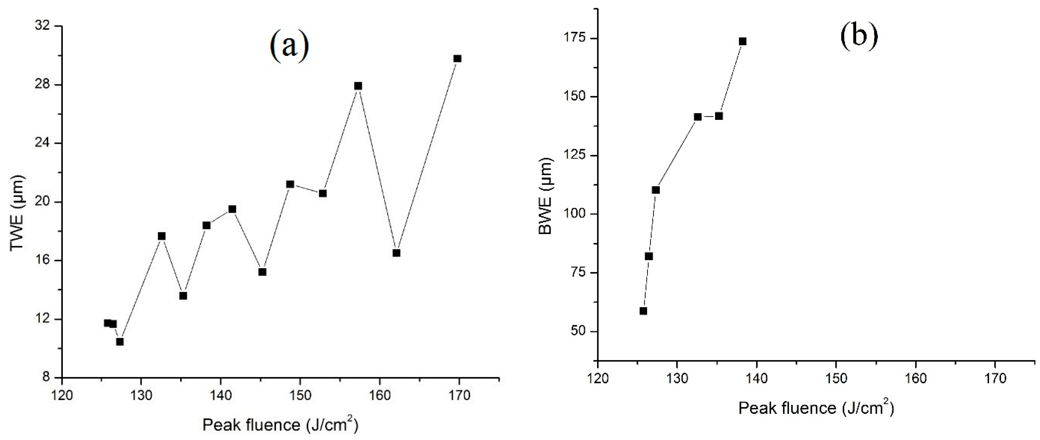
The microchannel width varied within a 210–229 µm range in the selected fluence range and the variation of TWE with varying peak fluence is shown in Figure 9a. The fluence range of 125–130 J/cm2 resulted in channels with width closer to the target width of 200 µm. The bottom width of the channel however varied drastically with peak fluence up to a certain fluence range after which any increase in peak fluence resulted in V-shaped microchannels. The variation of BWE with respect to peak fluence is shown in Figure 9b. The maximum width obtained at the bottom of the channel was 142 µm at a peak fluence of 125.76 J/cm2.
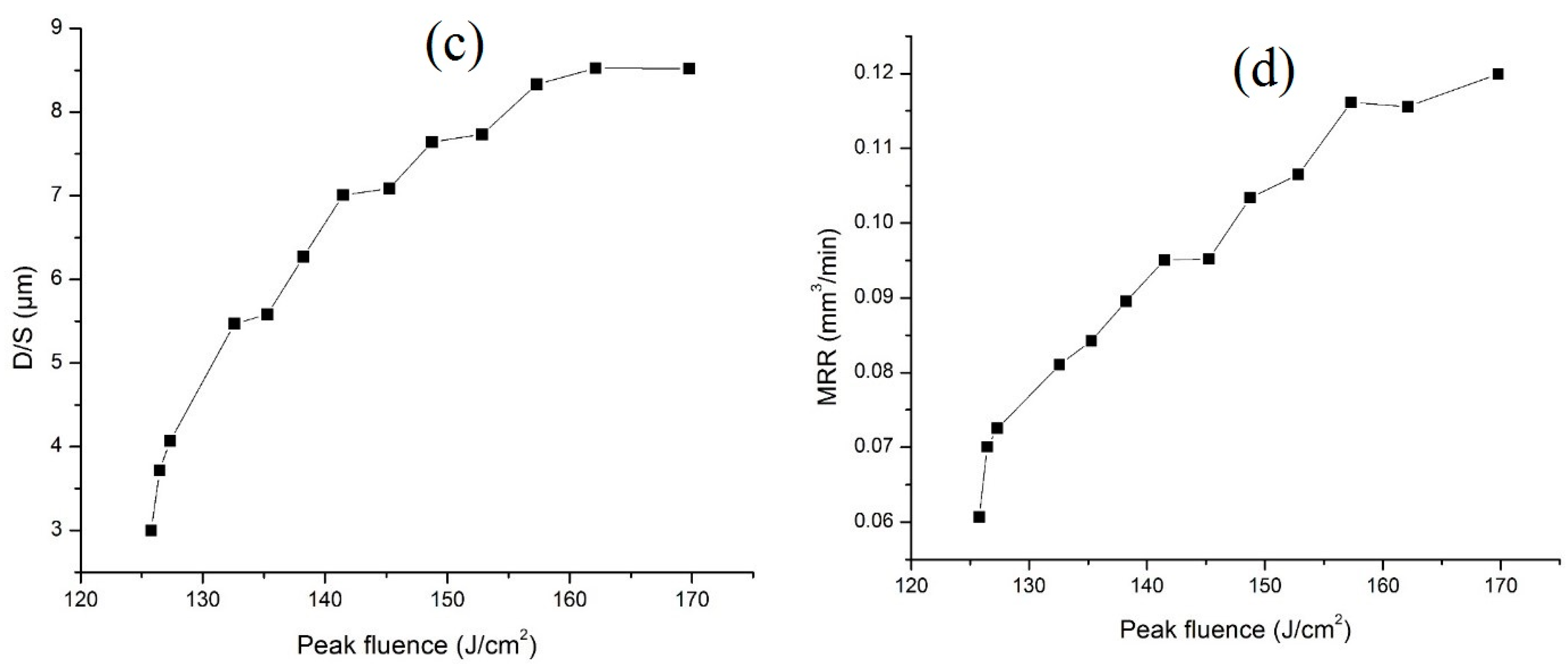
Depth per each laser scan increases with the increase in peak fluence as shown in Figure 9c. The increase is higher in the lower fluence range because the energy absorption into the material is higher at lower fluence, whereas in the high fluence range it reaches saturation limit hence there is minimum variation in depth removed. Depth per scan and total number of laser scans define the final depth of the channel. It is important in order to have the accurate depth of the channel. Depth per scan of less than 5 µm was found to give favorable results considering the TWE and BWE. A similar trend was observed for the MRR—it increases with the increase in peak fluence and the increase is quite significant in the lower fluence range as shown in Figure 9d.
Based on this study, the optimal peak fluence range for fabrication of microchannels was found to be 125–130 J/cm2. This peak fluence range resulted in microchannels with low dimensional error and medium depth of cut of about 3–5 µm.
3.3. Effect of Laser Scans on Channel Accuracy
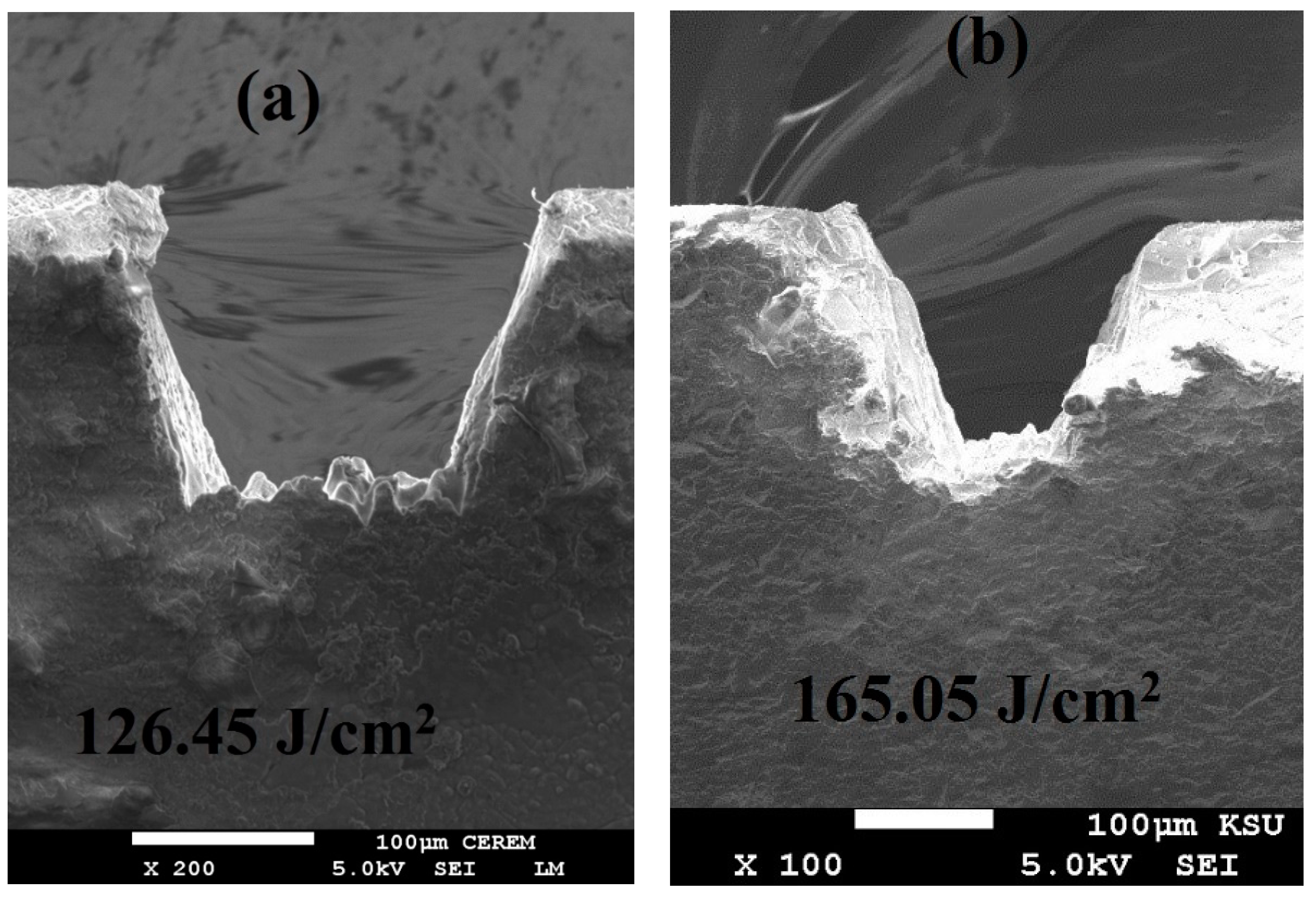
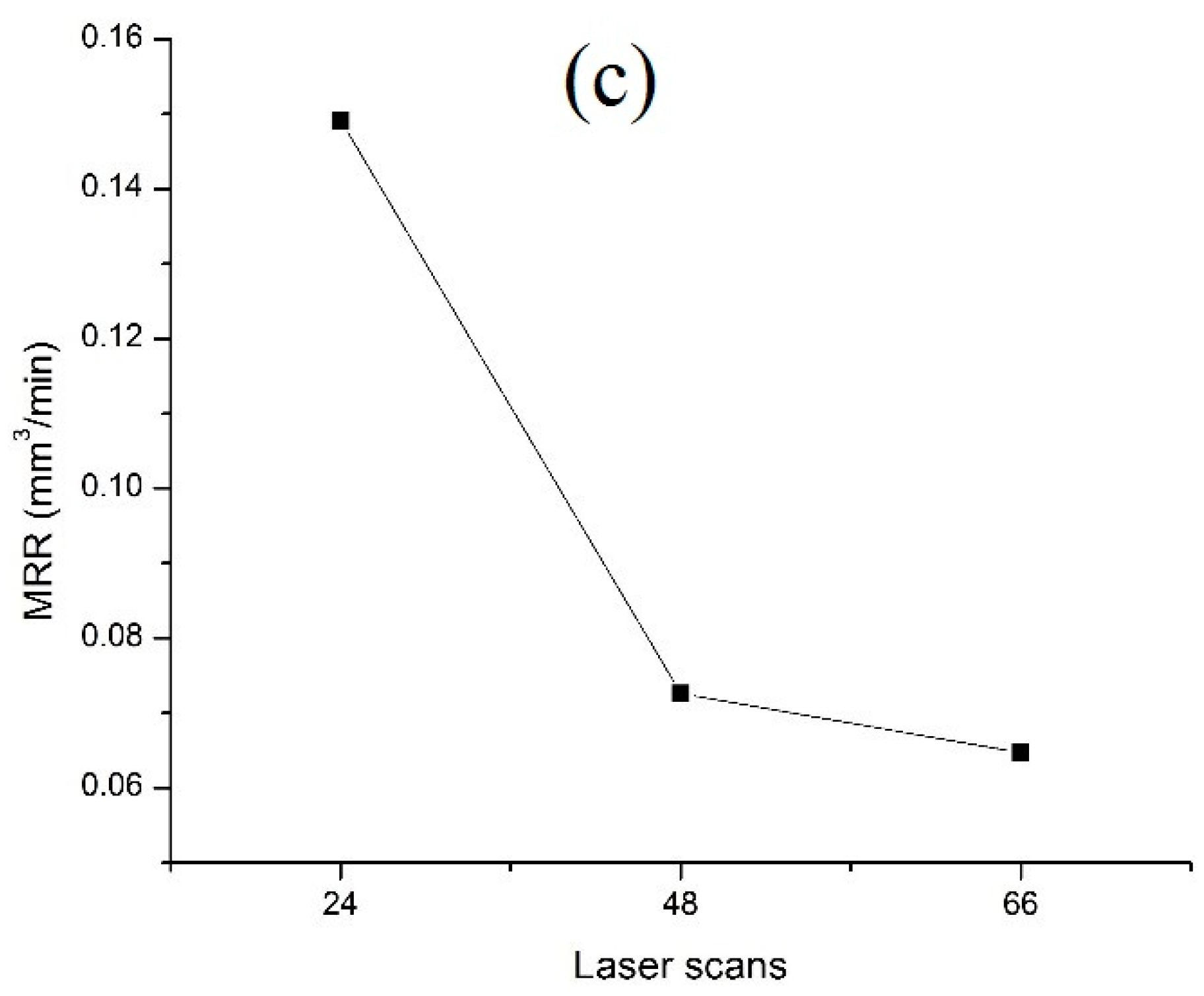
The number of laser scans along with depth per scan determine the final depth of the microchannel. This can be realized with different strategies such as a low number of scans with high depth per scan, a high number of scans in combination with low depth per scan or a medium depth per scan with medium laser scans. In order to study the effect of laser scans on microchannel accuracy, three different combinations of laser scans and depth per scan were tested for fabrication of microchannels with 200 µm width and 200 µm depth. Figure 10 shows the SEM images of the microchannel cross-section fabricated with 66 and 24 laser scans with 3 µm and 8 µm depth per scan respectively. The laser peak fluence was selected accordingly based up on the depth per scan. It can be seen that the geometry of the microchannel is more accurate with 3 µm depth per scan and 66 total scans. Higher depth per scan and lower laser scans resulted in a high degree of taper.
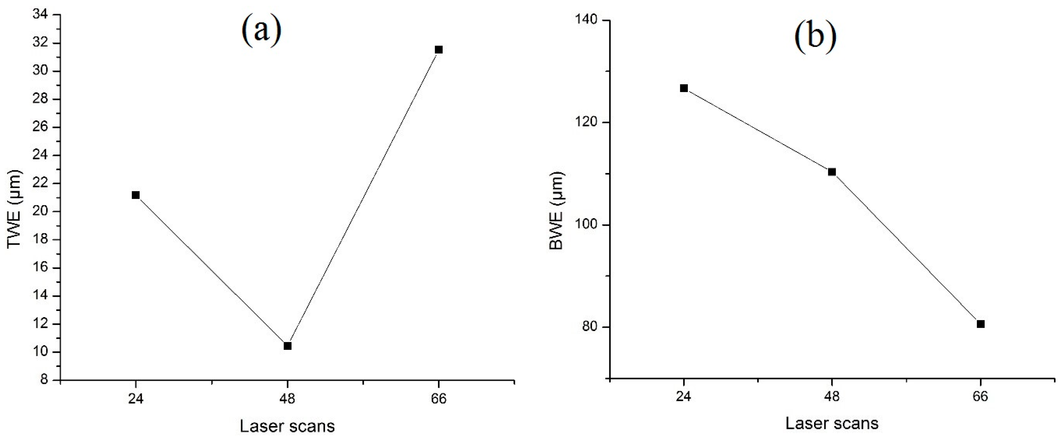
The microchannel geometry and MRR was found to vary with laser scans. Figure 11 shows the effect of laser scans on TWE, BWE, and MRR. In general, lower scans resulted in more accurate microchannels as compared to higher scans this is because with a lower number of laser scans the depth per scan and MRR is higher, which results in geometrical inaccuracies. However, the TWE was found to be minimum for the 48 laser scans suggesting that there exists an optimal number of scans for which the TWE is minimum. At a lower number of laser scans, the high depth of cut and MRR causes high TWE and with higher laser scans, the interaction of the laser beam with the edge is higher resulting in increased TWE. It can be seen that 66 laser scans in combination with 3 µm depth per scan resulted in microchannels with the least BWE and less taper. Figure 12 shows the SEM images of the microchannels fabricated using 3 µm depth per scan strategy with a peak fluence of 126.45 J/cm2. A total of 66 and 99 scans were carried out for the target depth of 200 µm and 300 µm respectively.
4. Conclusions
In this study the development of ceramic microchannels using an Nd:YAG laser was presented. In contrast to the previous research based on expensive low pulse width systems, this study assessed the performance of the Nd:YAG laser in the microsecond range to develop good quality microchannels in structural ceramics. It is evident that both the laser fluence and pulse overlap are significant parameters in controlling the quality and dimensional accuracy of microchannels. It was found that the depth of material removed per laser scan is an important indicator of the overall quality of the microchannels. Afterwards, a methodology was presented for obtaining good quality microchannels with targeted depth. The following conclusions can be drawn from the study:
- The size and quality of microchannels are found to be strongly dependent on laser peak fluence and pulse overlap.
- Irrespective of the peak fluence, high pulse overlaps give rise to high bottom width error (BWE) i.e., formation of V-shaped channels.
- Moderate pulse overlaps are recommended over low pulse overlap as they can fabricate good quality microchannels.
- Based on the analysis, a laser peak fluence of around 125–130 J/cm2 corresponding to 3–5 µm depth per scan is recommended for better accuracy.
- Low depth per scan values with a greater number of laser scans are recommended to achieve the desired depth.
Author Contributions
Conceptualization, M.K.M. and U.U.; Methodology, M.K.M., and U.U.; Software, M.K.M. and U.U.; Validation, M.K.M., U.U., and H.A.; Formal Analysis, M.K.M. and H.A.; Investigation, M.K.M., U.U., and O.A.; Resources H.A.; Data Curation, M.K.M. and U.U.; Writing—Original Draft Preparation, M.K.M. and U.U.; Writing—Review & Editing, M.K.M. and H.A.; Visualization, M.K.M.; Supervision, M.K.M. and U.U.; Project Administration, U.U. and O.A.; Funding Acquisition, H.A.
Funding
This research was funded by Deanship of Scientific Research at King Saud University, grant number RG-1440-026.
Acknowledgments
The authors extend their appreciation to the Deanship of Scientific Research at King Saud University for funding this work through research group number RG-1440-026.
Conflicts of Interest
The authors declare no conflicts of interest.
References
- Ritzhaupt-Kleissl, H.J.; Johander, P. Ceramics Processing in Microtechnology; Whittles Publishing: Dunbeath, UK, 2017. [Google Scholar]
- Basu, B.; Balani, K. Ceramics: Definition and Characteristics. In Advanced Structural Ceramics; Wiley: Hoboken, NJ, USA, 2011; pp. 3–10. [Google Scholar]
- Riedel, R.; Chen, I.-W. Ceramics Science and Technology: Synthesis and Processing; John Wiley & Sons, Incorporated: Hoboken, NJ, USA, 2011; Volume 3. [Google Scholar]
- Koç, M.; Ozel, T. Fundamentals of Micro-Manufacturing. In Micro-Manufacturing: Design and Manufacturing of Micro-Products; Koç, M., Ozel, T., Eds.; John Wiley & Sons: Hoboken, NJ, USA, 2011; pp. 1–23. [Google Scholar]
- Arkin, W.T. Advances in Laser and Optics Research; Nova Science Publishers: Hauppauge, NY, USA, 2012. [Google Scholar]
- Wu, B.; Ozel, T. Micro-laser processing. In Micro-Manufacturing: Design and Manufacturing of Micro-Products; Koç, M., Ozel, T., Eds.; John Wiley & Sons: Hoboken, NJ, USA, 2011; pp. 159–195. [Google Scholar]
- Bonse, J.; Geuss, M.; Baudach, S.; Sturm, H.; Kautek, W. The precision of the femtosecond-pulse laser ablation of TiN films on silicon. Appl. Phys. A 1999, 69, s399–s402. [Google Scholar] [CrossRef]
- Chen, T.C.; Darling, R.B. Parametric studies on pulsed near ultraviolet frequency tripled Nd: YAG laser micromachining of sapphire and silicon. J. Mater. Process. Technol. 2005, 169, 214–218. [Google Scholar] [CrossRef]
- Otani, T.; Herbst, L.; Heglin, M.; Govorkov, S.V.; Wiessner, A.O. Microdrilling and micromachining with diode-pumped solid-state lasers. Appl. Phys. A 2004, 79, 1335–1339. [Google Scholar] [CrossRef]
- Wernicke, T.; Krüger, O.; Herms, M.; Würfl, J.; Kirmse, H.; Neumann, W.; Behm, T.; Irmer, G.; Tränkle, G. Analysis of materials modifications caused by UV laser micro drilling of via holes in AlGaN/GaN transistors on SiC. Appl. Surf. Sci. 2007, 253, 8008–8014. [Google Scholar] [CrossRef]
- Okuchi, T.; Ohfuji, H.; Odake, S.; Kagi, H.; Nagatomo, S.; Sugata, M.; Sumiya, H. Micromachining and surface processing of the super-hard nano-polycrystalline diamond by three types of pulsed lasers. Appl. Phys. A 2009, 96, 833–842. [Google Scholar] [CrossRef]
- Mutlu, M.; Kacar, E.; Akman, E.; Akkan, C.K.; Demir, P.; Demir, A. Effects of the laser wavelength on drilling process of ceramic using Nd: YAG laser. J. Laser Micro Nanoeng. 2009, 4, 84–88. [Google Scholar] [CrossRef]
- Pan, C.T.; Hwang, Y.M.; Hsieh, C.W. Dynamic characterization of silicon-based microstructure of high aspect ratio by dual-prism UV laser system. Sens. Actuators A Phys. 2005, 122, 45–54. [Google Scholar] [CrossRef]
- Matsuoka, Y. Trepanning of glass using the fourth harmonic of nanosecond pulse Nd: YAG laser. Appl. Phys. A 2007, 88, 319–322. [Google Scholar] [CrossRef]
- Hu, W.; Shin, Y.C.; King, G.B. Micromachining of metals, alloys, and ceramics by picosecond laser ablation. J. Manuf. Sci. Eng. 2010, 132, 11009–11016. [Google Scholar] [CrossRef]
- Vukelić, S.; Kongsuwan, P.; Yao, Y.L. Ultrafast laser induced structural modification of fused silica—Part I: Feature formation mechanisms. J. Manuf. Sci. Eng. 2010, 132, 61012–61020. [Google Scholar] [CrossRef]
- Li, G.; Hu, S.; Tang, H.; Chen, B. Laser repeat drilling of alumina ceramics in static water. Int. J. Adv. Manuf. Technol. 2018, 96, 1–7. [Google Scholar] [CrossRef]
- Liu, Y.; Liu, L.; Deng, J.; Meng, R.; Zou, X.; Wu, F. Fabrication of micro-scale textured grooves on green ZrO2 ceramics by pulsed laser ablation. Ceram. Int. 2017, 43, 6519–6531. [Google Scholar] [CrossRef]
- Zhang, Y.; Wang, Y.; Zhang, J.; Liu, Y.; Yang, X.; Zhang, Q. Micromachining features of TiC ceramic by femtosecond pulsed laser. Ceram. Int. 2015, 41, 6525–6533. [Google Scholar] [CrossRef]
- Xing, Y.; Deng, J.; Lian, Y.; Feng, X. Femtosecond pulsed laser nanotexturing of Al2O3/TiC ceramic. Laser Phys. 2013, 23, 66002. [Google Scholar] [CrossRef]
- Xing, Y.; Deng, J.; Lian, Y.; Zhang, K.; Zhang, G.; Zhao, J. Multiple nanoscale parallel grooves formed on Si3N4/TiC ceramic by femtosecond pulsed laser. Appl. Surf. Sci. 2014, 289, 62–71. [Google Scholar] [CrossRef]
- Hanon, M.M.; Akman, E.; Oztoprak, B.G.; Gunes, M.; Taha, Z.A.; Hajim, K.I.; Kacar, E.; Gundogdu, O.; Demir, A. Experimental and theoretical investigation of the drilling of alumina ceramic using Nd: YAG pulsed laser. Opt. Laser. Technol. 2012, 44, 913–922. [Google Scholar] [CrossRef]
- Li, D.; Chen, X.; Guo, C.; Tao, J.; Tian, C.; Deng, Y.; Zhang, W. Micro surface texturing of alumina ceramic with nanosecond laser. Procedia Eng. 2017, 174, 370–376. [Google Scholar] [CrossRef]
- Xing, Y.; Liu, L.; Wu, Z.; Wang, X.; Huang, P.; Tang, L. Fabrication and characterization of micro-channels on Al2O3/TiC ceramic produced by nanosecond laser. Ceram. Int. 2018, 44, 23035–23044. [Google Scholar] [CrossRef]
Figure 1.
Schematic diagram of laser setup.

Figure 2.
Laser fluence with respect to lamp current.

Figure 3.
SME images showing microchannel cross-sections with varying pulse overlap at laser fluence of 169.76 J/cm2.
Figure 3.
SME images showing microchannel cross-sections with varying pulse overlap at laser fluence of 169.76 J/cm2.

Figure 4.
SEM images showing microchannel cross-sections with varying peak fluence at constant pulse overlap of 66.66%.
Figure 4.
SEM images showing microchannel cross-sections with varying peak fluence at constant pulse overlap of 66.66%.

Figure 5.
Effect of peak fluence and pulse overlap on TWE.

Figure 6.
Effect of peak fluence and pulse overlap on BWE.

Figure 7.
Effect of peak fluence and pulse overlap on depth per scan.

Figure 8.
Effect of peak fluence and pulse overlap on MRR.

Figure 9.
Effect of peak fluence on (a) TWE (b) BWE (c) D/S (d) MRR for the channels fabricated with 48 laser scans.
Figure 9.
Effect of peak fluence on (a) TWE (b) BWE (c) D/S (d) MRR for the channels fabricated with 48 laser scans.


Figure 10.
SEM images of microchannel cross-section fabricated with (a) 66 scans and (b) 24 scans.

Figure 11.
Effect of laser scans on (a) TWE (b) BWE (c) MRR.


Figure 12.
SEM images of the microchannels (a) 200 µm depth (b) 300 µm depth.


Table 1.
Laser specifications.
| Process Parameter | Process Condition |
|---|---|
| Wavelength | 1064 nm |
| Power | 30 W |
| Pulse width | 10 µs |
| Spot size | 30 µm |
| Pulse frequency | 6 kHz |
Table 2.
Design array of the microchannels fabricated by varying laser fluence and pulse overlap.
| S.no | Peak Fluence J/cm2 | Pulse Overlap % | Channel Width µm | Channel Depth µm | TWE µm | BWE µm | D/S µm | MRR mm3/min |
|---|---|---|---|---|---|---|---|---|
| 1 | 136.755 | 58.33 | 218.3 | 124.6 | 18.3 | 67.4 | 5.2 | 0.119 |
| 2 | 169.765 | 58.33 | 227.5 | 194.4 | 27.5 | 74.2 | 8.1 | 0.189 |
| 3 | 229.183 | 58.33 | 240.1 | 239.0 | 40.1 | 62.8 | 10.0 | 0.248 |
| 4 | 353.678 | 58.33 | 253.8 | 305.2 | 53.8 | 62.8 | 12.7 | 0.333 |
| 5 | 517.313 | 58.33 | 251.5 | 437.8 | 51.5 | 97.1 | 18.2 | 0.470 |
| 6 | 136.755 | 66.66 | 207.7 | 120.9 | 7.7 | 67.7 | 5.0 | 0.088 |
| 7 | 169.765 | 66.66 | 222.7 | 246.7 | 22.7 | 112.1 | 10.3 | 0.160 |
| 8 | 229.183 | 66.66 | 233.8 | 282.0 | 33.8 | 86.5 | 11.7 | 0.224 |
| 9 | 353.678 | 66.66 | 238.2 | 442.3 | 38.2 | 133.9 | 18.4 | 0.320 |
| 10 | 517.313 | 66.66 | 249.3 | 610.8 | 49.3 | 164.5 | 25.4 | 0.382 |
| 11 | 136.755 | 75 | 228.6 | 307.5 | 28.6 | 12.8 | 0.118 | |
| 12 | 169.765 | 75 | 233.2 | 385.3 | 33.2 | 16.1 | 0.146 | |
| 13 | 229.183 | 75 | 242.4 | 479.0 | 42.4 | 20.0 | 0.204 | |
| 14 | 353.678 | 75 | 254.9 | 698.4 | 54.9 | 29.1 | 0.312 | |
| 15 | 517.313 | 75 | 253.8 | 958.1 | 53.8 | 39.9 | 0.406 |
Table 3.
Design array of the microchannels fabricated by varying the laser fluence for 48 laser scans at a fixed pulse overlap of 66.66%.
Table 3.
Design array of the microchannels fabricated by varying the laser fluence for 48 laser scans at a fixed pulse overlap of 66.66%.
| S.no | Fluence J/cm2 | Channel Width µm | Channel Depth µm | TWE µm | BWE µm | D/S µm | MRR mm3/min |
|---|---|---|---|---|---|---|---|
| 1 | 125.768 | 211.7 | 144.0 | 11.7 | 58.6 | 3.0 | 0.0607 |
| 2 | 126.455 | 211.7 | 178.3 | 11.7 | 82.1 | 3.7 | 0.0701 |
| 3 | 127.324 | 210.4 | 195.3 | 10.4 | 110.3 | 4.1 | 0.0725 |
| 4 | 132.590 | 217.7 | 262.6 | 17.7 | 141.4 | 5.5 | 0.0811 |
| 5 | 135.287 | 213.6 | 267.8 | 13.6 | 141.9 | 5.6 | 0.0843 |
| 6 | 138.227 | 218.4 | 301.0 | 18.4 | 173.7 | 6.3 | 0.0895 |
| 7 | 141.471 | 219.5 | 336.4 | 19.5 | 7.0 | 0.0951 | |
| 8 | 145.244 | 215.2 | 340.1 | 15.2 | 7.1 | 0.0952 | |
| 9 | 148.733 | 221.2 | 366.8 | 21.2 | 7.6 | 0.1034 | |
| 10 | 152.841 | 220.6 | 371.2 | 20.6 | 7.7 | 0.1065 | |
| 11 | 157.302 | 227.9 | 400.0 | 27.9 | 8.3 | 0.1161 | |
| 12 | 162.124 | 216.5 | 409.2 | 16.5 | 8.5 | 0.1156 | |
| 13 | 169.765 | 229.8 | 409.1 | 29.8 | 8.5 | 0.1199 |
© 2019 by the authors. Licensee MDPI, Basel, Switzerland. This article is an open access article distributed under the terms and conditions of the Creative Commons Attribution (CC BY) license (http://creativecommons.org/licenses/by/4.0/).
Share and Cite
MDPI and ACS Style
Mohammed, M.K.; Umer, U.; Abdulhameed, O.; Alkhalefah, H. Effects of Laser Fluence and Pulse Overlap on Machining of Microchannels in Alumina Ceramics Using an Nd:YAG Laser. Appl. Sci. 2019, 9, 3962. https://doi.org/10.3390/app9193962
AMA Style
Mohammed MK, Umer U, Abdulhameed O, Alkhalefah H. Effects of Laser Fluence and Pulse Overlap on Machining of Microchannels in Alumina Ceramics Using an Nd:YAG Laser. Applied Sciences. 2019; 9(19):3962. https://doi.org/10.3390/app9193962
Chicago/Turabian StyleMohammed, Muneer Khan, Usama Umer, Osama Abdulhameed, and Hisham Alkhalefah. 2019. "Effects of Laser Fluence and Pulse Overlap on Machining of Microchannels in Alumina Ceramics Using an Nd:YAG Laser" Applied Sciences 9, no. 19: 3962. https://doi.org/10.3390/app9193962
Note that from the first issue of 2016, this journal uses article numbers instead of page numbers. See further details here.