Article

A Proposal for Evading the Measurement Uncertainty in Classical and Quantum Computing: Application to a Resonant Tunneling Diode and a Mach-Zehnder Interferometer

1
Departament d’Enginyeria Electrònica, Universitat Autònoma de Barcelona, 08193-Bellaterra (Barcelona), Spain
2
Dipartimento di Scienze Fisiche, Informatiche e Matematiche, Università degli Studi di Modena e Reggio Emilia, Via Campi 213/A, I-41125 Modena, Italy
3
Max Planck Institute for the Structure and Dynamics of Matter and Center for Free-Electron Laser Science, Luruper Chaussee 149, 22761 Hamburg, Germany
4
S3, Istituto Nanoscienze-CNR, Via Campi 213/A, 41125 Modena, Italy
*
Author to whom correspondence should be addressed.
Appl. Sci. 2019, 9(11), 2300; https://doi.org/10.3390/app9112300
Submission received: 8 April 2019 / Revised: 7 May 2019 / Accepted: 29 May 2019 / Published: 4 June 2019
(This article belongs to the Special Issue (Quantum) Physical Informatics)

Abstract

:
Measuring properties of quantum systems is governed by a stochastic (collapse or state-reduction) law that unavoidably yields an uncertainty (variance) associated with the corresponding mean values. This non-classical source of uncertainty is known to be manifested as noise in the electrical current of nanoscale electron devices, and hence it can flaw the good performance of more complex quantum gates. We propose a protocol to alleviate this quantum uncertainty that consists of (i) redesigning the device to accommodate a large number of electrons inside the active region, either by enlarging the lateral or longitudinal areas of the device and (ii) re-normalizing the total current to the number of electrons. How the above two steps can be accommodated using the present semiconductor technology has been discussed and numerically studied for a resonant tunneling diode and a Mach-Zehnder interferometer, for classical and quantum computations, respectively. It is shown that the resulting protocol formally resembles the so-called collective measurements, although, its practical implementation is substantially different.

1. Introduction

Assessing the future of emergent technologies is not an easy task. Today there is a lively debate in the scientific community about whether classical or quantum computing will offer better performance in the coming future. At present, the field effect transistor is still the most efficient device to perform classical computations. The electronic industry is able to fit 10 10 transistors all together in a single chip, working at frequencies of a few GHz [1]. State-of-the-art transistors, with nanoscale dimensions, are quantum devices in the sense that their ability to convert the input into output information is based on quantum laws governing electron transport [2]. In digital binary classical computing, the logical state ‘1’ is encoded into a value of a well-defined measurable physical property of the transistor, while the logic state ‘0’ corresponds to a different value of such property. Usually the physical properties used in electron devices for classical computing are the electrical current or the voltage in different (input and output) terminals. It is important to notice that although the transistor is a quantum device whose performance is determined by the evolution of quantum states, these quantum states are not directly used to encode information in classical computing.
In quantum computing [3], contrarily, the logical state ‘1’ is directly encoded in a quantum state of the physical system, namely | 1 ψ 1 ( r , t ) where r represents the degrees of freedom of the system. Similarly, the logical state ‘0’ corresponds to another quantum state | 0 ψ 0 ( r , t ) . Because of the quantum superposition principle, a sum of the two physical states, a | 1 + b | 0 where a and b are complex numbers, is also a valid physical state of the system. As a consequence, quantum mechanics offers the possibility of operating simultaneously on the logical states ‘1’ and ‘0’. This opens classically inaccessible computing possibilities.
Many companies and researchers are advocating for quantum computing. Among many others, for example, Google has said that its state-of-the-art quantum chip will be the first to perform calculations beyond the best existing classical supercomputers [4]. Other companies and researchers, on the contrary, understand quantum computing as an exciting discipline, with an unquestionable scientific interest, but argue that quantum technologies will not substitute our classical computing machines at home (because quantum computers are complex, expensive and built using a more immature technology) [5,6]. In any case, without making any risky prediction, what seems clear today is that classical and quantum computing are both valuable research avenues.
Any classical or quantum computation using quantum devices is implemented following three main steps: (i) initial preparation of the quantum state, (ii) unitary evolution of the state and (iii) the final measurement of the state. In this paper, we will focus on the last step for both classical and quantum computations. The measurement step is linked to the quantum uncertainty [7] that implies a practical inconvenience since it gives rise to quantum noise at the output of the device (The reader can argue that the uncertainty disappears when the quantum state is prepared as an eignestate of the projective (measuring) operator. However, typically, the preparation of the state of an electron being injected into the active device region from the contact (reservoir) is done by the contacts itself, which do not provide such eigenstates). Solid-sate quantum electron devices are unquestionably the best technology to implement classical computing. It is, however, not clear today which will be the best technology for quantum computing. In any case, it seems clear that the possibility of implementing quantum computing algorithms with solid-sate devices would benefit from the maturity of the existing technology and offers the possibility of making quantum computing platforms compatible with classical ones.
The paper is structured as follows. In Section 2, we will propose a simple protocol that allows evading the quantum uncertainty associated with the measurement process in quantum electron devices, for either classical or quantum computing applications. This is the main result of this work. In Section 3, we will first investigate the measurement of the electrical current under this protocol for a resonant tunneling diode (RTD) understood as a quantum electron device useful for classical computing. Later, in Section 4, we will analyze the measurement of the electrical current in a Mach-Zehnder interferometer (MZI) which is tailored to design the logic gates suitable for implementing quantum computing. We will conclude in Section 5. More technical details are presented in the appendices.

2. Quantum Uncertainty: The Problem and the Solution

In this section, in order to simplify the discussion and better understand the problem and the solution explained here, we made the following simplifying assumptions. First, we will focus on a quantum electron device with just one degree of freedom indicated by r . The consideration of more realistic situations, with many degrees of freedom in a quantum device, would not modify the conclusions drawn here and would only complicate the notations and understanding of the results. See Appendix A for the straightforward generalization of the present results to an unmodified (original) quantum device with many degrees of freedom in the active region.
Second, we will assume that the measurement of the electrical current of the quantum electron device is done through a projective (strong) operator and that the state of the system after the measurement is just an eigenstate of this operator. In other words, we will assume that the measurement process is done with a projective value measure (PVM), while it has been argued that the realistic type of measurement of the electrical current is better described by a positive operator valued measure (POVM) [8,9]. In any case, the explicit consideration of a POVM to describe the measurement process will not add any relevant point in the discussion. In Appendix C, we explain with more detail the measurement of the electrical current in a realistic quantum electron device as a POVM.

2.1. The Problem

The first step to implement a classical or quantum computing algorithm using quantum devices is the initial preparation of the quantum state associated with the quantum electron device ψ i n ( r , 0 ) . In quantum computing, the initial state is directly linked to a combination of two states, ψ 1 ( r , 0 ) and ψ 0 ( r , 0 ) , respectively associated with the logical values ‘1’ and ‘0’, whereas in classical computing, the link between logical information and initial quantum state is not direct. Typically, a quantum device for classical computation is connected to the external world through the contacts (also know as reservoirs) that determine the electron wave function depending on temperature and doping conditions. The input logical information is then linked to a value of an observable I, not directly to the quantum state. We have used the symbol I to remind readers that hereafter, we will consider the electrical current as the physical magnitude where information is encoded.
The second step is the manipulation of the initial quantum state through the quantum electron device (also known as gate in the literature). Typically, such manipulation, whether in classical or quantum computing is done through a (usually unitary) operator U ^ ( t , 0 ) . In quantum computing, the final state ψ o u t ( r , t ) = U ^ ( t , 0 ) ψ i n ( r , 0 ) is directly linked to the output logical information, while in classical computing the output logical information is linked to an observable I associated with this final state through a measurement process that we describe below. See Figure 1a where different gates of an RTD which are connected to exemplify a classical computation gate connected through output values of the electrical current (or voltage), while the connection among different gates of the quantum computing device is done through the wave function itself as depicted in Figure 1b.
The third and last step, both in classical or quantum computing algorithms, is the measurement step. To get the final observable value I in classical computing, the quantum electron device has to be measured through a (non-unitary) process. Such non-unitary process is depicted as an ammeter in Figure 1. The evolution from the final state to the measured state, ψ o u t ( r , t ) ψ I ( r , t ) , is called collapse or reduction of the wave function. The subindex I here refers to the measured state of the current which corresponds to an eigenvalue I of the eigenfunction ψ I ( r , t ) associated with the operator I ^ . In quantum computing, the final wave function ψ o u t ( r , t ) is not directly measurable in a single shot measurement. Instead, the logical information assigned to this final quantum state has to be indirectly deduced from the measurement of an observable assigned to such final state. See Figure 1b. Notice that the measurement in quantum computing has to be done only once, at the end of the gate, because each measurement collapses the wave function, destroying the required superpositions of different states in the quantum computing algorithms.
The process of measurement involves a quantum uncertainty which is a consequence of the fact that each time a quantum measurement is done, the wave function collapses into an eigenstate of the operator I ^ associated with the measuring apparatus. The observable output I o u t is a random value equal to the eigenvalue associated with the mentioned eigenstate. In general, and this is true for the measurement of the electrical current, the final state before measurement ψ o u t ( r , t ) is not an eigenstate of the current ψ I ( r , t ) ψ o u t ( r , t ) . In fact, the final state can be written as a superposition of many different current eigenstates. Thus, each time we repeat an experiment to obtain information about the output current, we get different values. This randomness in the output values can be quantified through the probability distribution P ( I ) = | ψ I ( r ) | ψ o u t ( r , t ) | 2 given by Born’s law. From a quantum engineering point of view, this quantum uncertainty (seen as noise in the current) is inconvenient for efficiently processing logical (either classical or quantum) information.
In classical computations, the uncertainty on the electrical current can be eliminated by using the ensemble value of the current I computed from a large number of identical experiments, each one giving I i , with the subindex i identifying the experiment. The ensemble value is defined as I = ( i = 1 N e x p I i ) / N e x p , where N e x p is the number of experiments. In principle, this ensemble value would require repeating the same experiment for a large set of N e x p identical quantum electron devices. In practice, by invoking ergodic arguments, the repetition of the experiment is substituted by measuring at different times in the same quantum electron device. Thus, instead of defining the signal of the output logical value as the instantaneous current I 1 (which has noise) one defines it as the DC value of the electrical current I computed during a large time interval (which has no noise). This solution is efficient for reducing the noise, but it requires a large measuring time. (In our simulation example with an RTD with a device active region length of 10 nm, the injection time of 0.05 ps and the velocity of electrons as 10 4 m/s, the time after which we get the non-fluctuating value of the current is around 50 ps. In any case, the measuring time is again a parameter that depends on many factors, like injection time, velocity of electrons, electron density, level of tolerable uncertainty. etc., and that can be enlarged or reduced as desired by manipulating these parameters.)
The quantum uncertainty described above represents also a problem for quantum computing. In fact, although the logical output information in quantum computing is encoded in the final wave function ψ o u t ( r , t ) (not in an observable I i ), the quantum state ψ o u t ( r , t ) is not itself an observable (i.e., it cannot be measured in a single shot measurement). Thus, the quantum state of the system needs to be deduced from the expectation value I . Again, the measurement process of such observable I has the same inconveniences mentioned above for classical computing, due to the quantum uncertainty. We notice that in a quantum computing algorithm, with many interconnected quantum gates, the measurement of the observable is done only at the last gate. In fact, trying to measure at an intermediate gate would be understood as a type of decoherent phenomena that would dramatically perturb the unitary evolution required in typical quantum algorithms. In Figure 1 we encircle the regions of the connected gates where the dynamics of electrons are supposed to be governed by unitary quantum evolutions. From Figure 1, one can understand why decoherence is a serious problem for quantum computing, but not for classical computing. In an array of interconnected classical computing devices, the decoherence that can appear at the output of each particular device due to the measurement does not affect the performance of the algorithm because the interconnection between devices is done in terms of observables (not in terms of wave functions).
In summary, the electrical current in nanoscale devices, for classical or quantum computing, has an inherent quantum uncertainty, seen as noise in the measured value of the electrical current. Since the information is usually encoded in the average value I of the electrical current, we require an effort to wash out the noise from the measured current to get valid information. The typical solution in the literature to wash out the noise is repeating the experiment many times (or using the ergodic theorem to get I after a large time).

2.2. The Solution

In this work, we explain a novel solution to the problem discussed above about reducing the quantum noise induced by the measurement process. We argue in this paper that such noise can be eliminated by modifying the quantum device to accommodate N electrons, simultaneously. We will show that the dispersion of a random distribution of the (normalized) electrical current of N electrons tends to zero, which implies eliminating the quantum noise.
Let us consider an original or unmodified quantum electron device (before applying our protocol) that has only one transport electron, at each time, responsible for the measured current. Such electron at time t i n is described by a single particle quantum state | ψ 1 ( t i n ) where the superindex 1 refers to this first electron. We are measuring the current through a single particle operator I ^ 1 . If the state | ψ 1 ( t i n ) is not an eigenstate of the operator I ^ , then, the measurement of the I gives rise to the quantum noise discussed in the previous subsection (we notice again that the generalization to more electrons is done in Appendix A).
The solution that we propose to minimize the quantum noise requires designing a new quantum device (that we will refer to as the modified quantum device or just the quantum device) so that this new device satisfies the following two conditions:
  • Condition 1: We enlarge the original quantum electron device in order to accommodate a large number of electrons N simultaneously. Then, the many-particle wave function Ψ T ( t i n ) that defines this N electrons at time t i n is:
    | Ψ T ( t i n ) = | ψ 1 ( t i n ) | ψ 2 ( t i n ) . | ψ N ( t i n ) ,
    where the wave function | ψ i ( t i n ) is the single electron wave function that corresponds to the i-th electron prepared under the same conditions that we have used to prepare the wave function | ψ 1 ( t i n ) in the original quantum electron device.
    Strictly speaking, the condition N is inaccessible in a practical scenario. We will see numerically in the following sections that a finite number of electrons is enough to drastically reduce the quantum noise. Identically, if the number of transport electrons in the original (unmodified) quantum electron device is already larger than one, the solution proposed here is still perfectly valid. See Appendix A for a generalization of the present protocol to more than one electron in the unmodified electron device. Finally, as can be seen in Equation (1), we assume a many-particle wave function of non-interacting electrons. This is obviously an approximation in realistic quantum devices since these electrons will suffer exchange and Coulomb interactions. In Appendix D, we test our protocol under the exchange symmetry for two electrons. Under the assumption of an initial negligible overlap of the wavepackets our protocol does not deviate from the actual result. These issues will be further elaborated in the practical implementation of this protocol in next two section.
    We mention that some (small) variation in the preparation of the state | ψ 1 ( t i n ) , | ψ 2 ( t i n ) ,… forming Ψ T ( t i n ) is allowed. For example, the time delay between the injection of different single electron wave packets can vary. Also the central position of the wave packets along the lateral dimension of the device can be different. Similarities between different wave packets have to be enough to justify that the probability distribution of the values of the current is identical for all single electron wave packets.
  • Condition 2: We substitute the measuring apparatus associated with the single particle operator I ^ 1 with a new measuring apparatus whose associated many-body operator I ^ T is:
    I ^ T = I 1 ^ + I 2 ^ + . + I N ^ N ,
    where I i ^ = I ^ . I ^ i I ^ acts only on the quantum state | ψ i ( t i n ) and I ^ is the identity operator in the small Hilbert space of each degree of freedom. Notice the presence of the factor N in the denominator of the operator I ^ T .
    In next section, we will show the physical soundness of the many-particle operator in Equation (2) for typical semiconductor electron device technology.
Now let us formally demonstrate that the dispersion of the electrical current of the modified quantum device (satisfying condition 1 and condition 2) is zero. For the operator I ^ T defined in Equation (2), we calculate the variance of the I T 2 as the mean square value of the operator I ^ T as:
Ψ T | ( I ^ T ) 2 | Ψ T = 1 N 2 i N ψ i | I ^ i I ^ i | ψ i + i , j i N 1 N 2 ψ i | I ^ i | ψ i ψ j | I ^ j | ψ j .
By construction of the wave function in Equation (1), we know that the mean values ψ j | I ^ j | ψ j are all identical for any j. Therefore, we can consider ψ j | I ^ j | ψ j = ψ 1 | I ^ 1 | ψ 1 because all electrons are described by the same wave function and we can rewrite Equation (3) as follows,
Ψ T | ( I ^ T ) 2 | Ψ T = N N 2 ψ 1 | ( I ^ 1 ) 2 | ψ 1 + N ( N 1 ) N 2 ψ | I ^ 1 | ψ 1 ψ 1 | I ^ 1 | ψ .
Therefore, when N , we get:
I ^ T 2 = Ψ T | ( I ^ T ) 2 | Ψ T = ψ 1 | I ^ 1 | ψ 1 ψ 1 | I ^ 1 | ψ 1 = I ^ 1 2 .
Now, we have to demonstrate that the logical information provided by the modified quantum device dealing with I T is the same as the one that one gets from the original quantum device. As we discussed, the logical information of the original quantum device was represented by the mean value of the current I ^ 1 and not by the instantaneous value I 1 (which was too noisy due to quantum uncertainty). It is quite simple to demonstrate that I T = I ^ 1 for N . By construction, we know I ^ 1 = I ^ j , from Equation (2) we get I ^ T = N I 1 / N = I ^ 1 and with Equation (5), we conclude that the dispersion σ I T of the distribution of the total current I T is zero:
σ I T 2 = I ^ T 2 I ^ T 2 = 0 .
The result σ I T = 0 in Equation (6) implies that the distribution of I T is a delta function around I ^ 1 . This implies that in every measurement one gets the mean value of the single particle average current I T = I 1 .
It can be easily checked that the state in Equation (1) in the limit N is, in fact, an eigenstate of any operator of the type of Equation (2) at any time. This state, with this unusual property, has been used by one of the co-authors to study the quantum-to-classical transition [10]. In addition, a similar state and operator as the ones invoked in our condition 1 and condition 2 has been used to develop the new concept of collective measurements [11,12]. Such collective measurements do really invoke multiple physical repetitions of the quantum system, while in our paper we make use of this idea in the same many-particle state and operator and in a single (modified) quantum device. In other words, the demonstration provided above is mathematically equivalent to the one that appears in the theory of collective measurements, but their physical implementation in the laboratory is radically different. In the rest of the paper, we will show how these two conditions can be effectively implemented with the semiconductor electron device technology in a single device for classical and quantum computing.

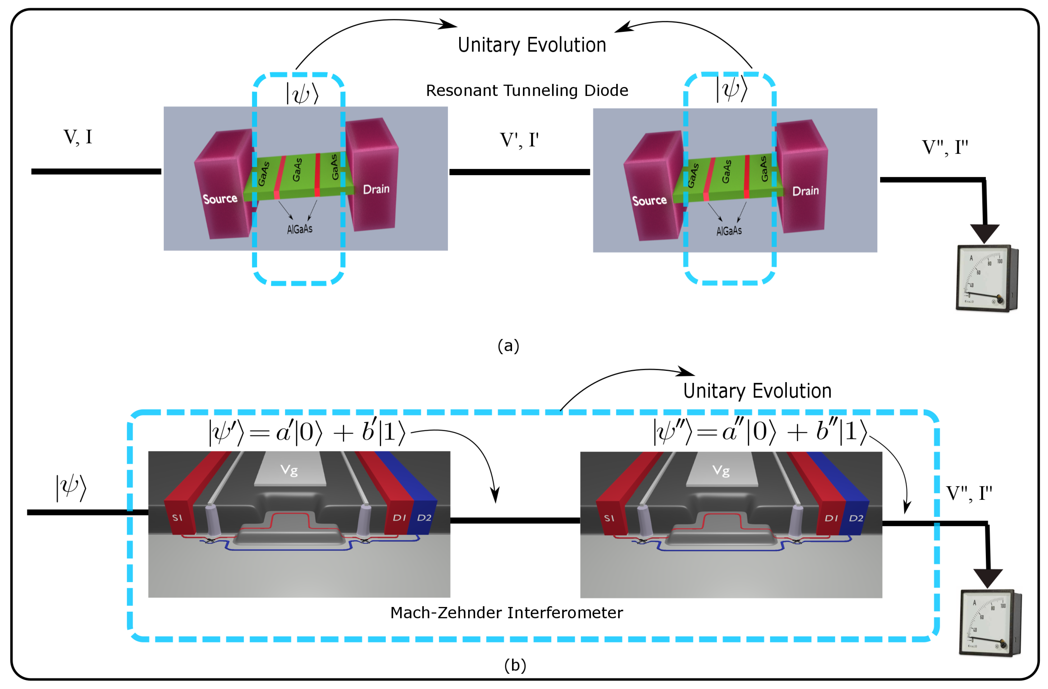
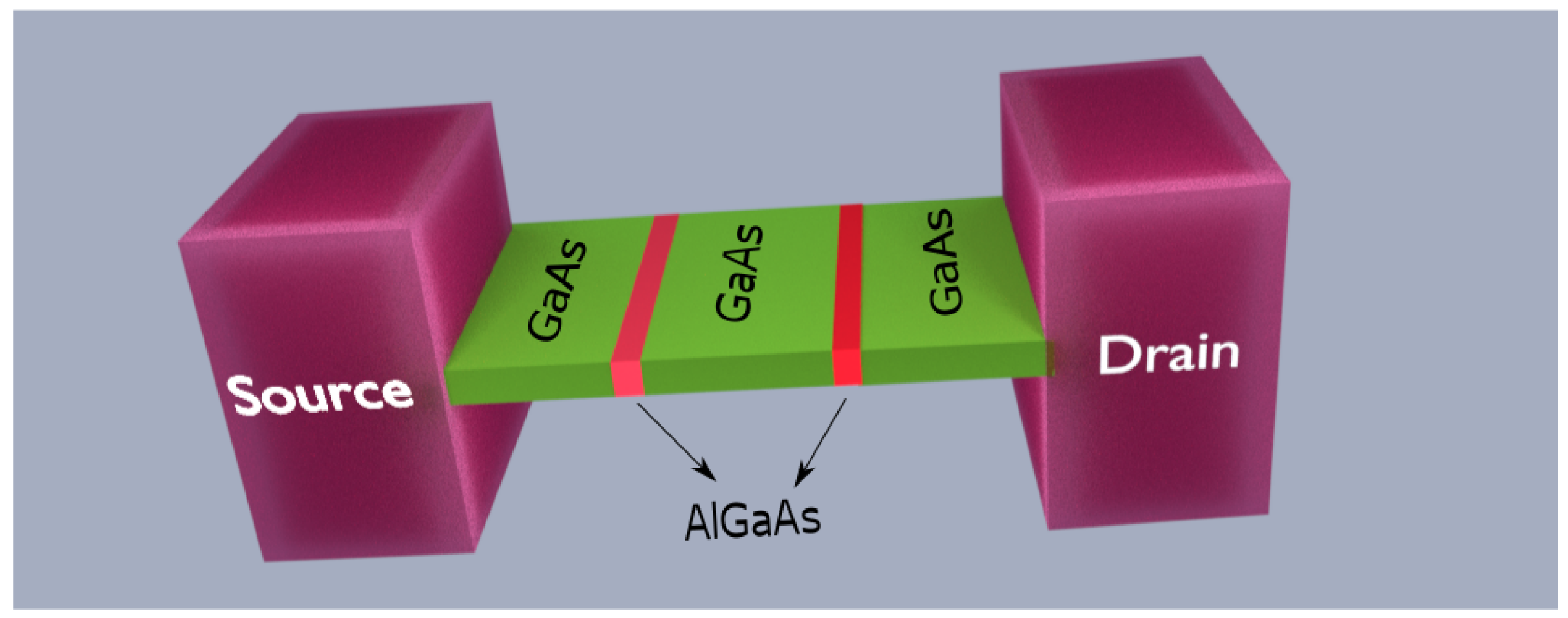
3. Application to Classical Computing Device: Resonant Tunneling Diode

As an example for the application of the discussed protocol in a classical computing device, we consider the computation of the electrical current in an RTD. This type of electron device is a pure quantum device, whose performance is based on tunneling, and has been successfully implemented in some particular high frequency applications particularly to explore the missing THz gap for various analog and digital applications [13,14,15,16]. The main element that defines an RTD is a double barrier potential created, for example, by alternating Gallium Arsenide (GaAs) and Aluminum Gallium Arsenide (AlGaAs) III-V semiconductors with different energy gaps, as shown in Figure 2. The combination of low band gap and high band gap semiconductors leads to the formation of a well in the potential energy profile, which gives rise to discrete set of energies inside, known as resonant energies.
As depicted in Figure 2, two reservoirs or contacts emit or collect the electrons through the RTD structure. We name the left contact as source (also known as emitter in the literature) and the right contact as drain (also known as collector in the literature). These contacts are responsible for the first step of classical computing algorithm: the preparation of the initial quantum states. The energy of the injected electrons is determined by the Fermi-Dirac statistics (depending on the doping conditions of the contacts). A regular injection of electrons is assumed according to the discussion of the Appendix B. The second step of the classical computing algorithm is carried out by the barrier structure that determines whether the injected electrons are effectively transmitted or not. An electron incident on the double barrier with an energy equal to one of the resonant energies tunnels through the barrier, being transmitted with a transmission coefficient T close to one, while electrons with other energies have a transmission coefficient close to zero. An external potential between the drain and source potentials, modifies the double barrier potential energy profile, controlling the ON and OFF currents. One value of the current can be assigned to the logical output information ’1’ and the other to the ’0’.
The last step of the classical computing algorithm is the measurement of the ON or OFF current which implies the measurements (collapse) of the quantum wave function assigned to electrons inside the RTD, which provides the undesired quantum uncertainty in the output values of the current. We discuss next how the conditions of Section 2.2 can be implemented.

3.1. Implementation of Condition 1 and Condition 2

We consider that the RTD depicted in Figure 2 corresponds to the modified design of the device that accommodates a large number of N electrons simultaneously inside. In this particular device, enlarging the lateral area A is enough to enlarge the number of electrons inside the RTD. We can reasonable assume that the contact prepares the wave packets of each electron in a similar way so that the condition 1 of our protocol in Equation (1) is easily satisfied. Certainly, a point that requires further discussion is how to ensure that the many-body wave function of electrons in the active region of this modified device can be approximated by the non-interacting wave function in Equation (1). In the Appendix A and Appendix B some qualitative indications are mentioned. A different solution for minimizing the undesired Coulomb and exchange interactions will be discussed in next section, for quantum computing.
To satisfy the second condition we have to ensure that all electrons inside the device contribute equivalently to the measured value of the electrical current. A detailed discussion of the conditions that have to be satisfied by the quantum device to ensure this point is provided in the Appendix C. We anticipate here that such discussion is greatly simplified by associating to each electrons a quantum (Bohmian) trajectories, whose positions and velocities are well-defined even in absence of a measurement, in addition to the orthodox wave function. Then, the electrical current due to the simultaneous contribution of all electron leads to the following expression,
I e x p ( t ) = i = 1 N ( t ) I i ( t ) = i = 1 N ( t ) q v x i ( t ) L ,
As discussed in the Appendix C the above expression assumes that the lateral dimensions of the (two terminal) electron device are much larger than the longitudinal one, and that the contacts are formed by metals with a fast screening time in comparison with that on the active region. The condition 2 of our protocol to define the current operator as in Equation (2), requires to define the output instantaneous value of the current as,
I T ( t ) = I e x p ( t ) N ( t ) ,
The value of N ( t ) N can be assumed to be proportional to the enlarged lateral area, and the value I T ( t ) computed from I e x p ( t ) after knowing the ratio of the modified/unmodified areas. The detailed discussion on the definition of the current and the implications of condition 2 is given in Appendix C.

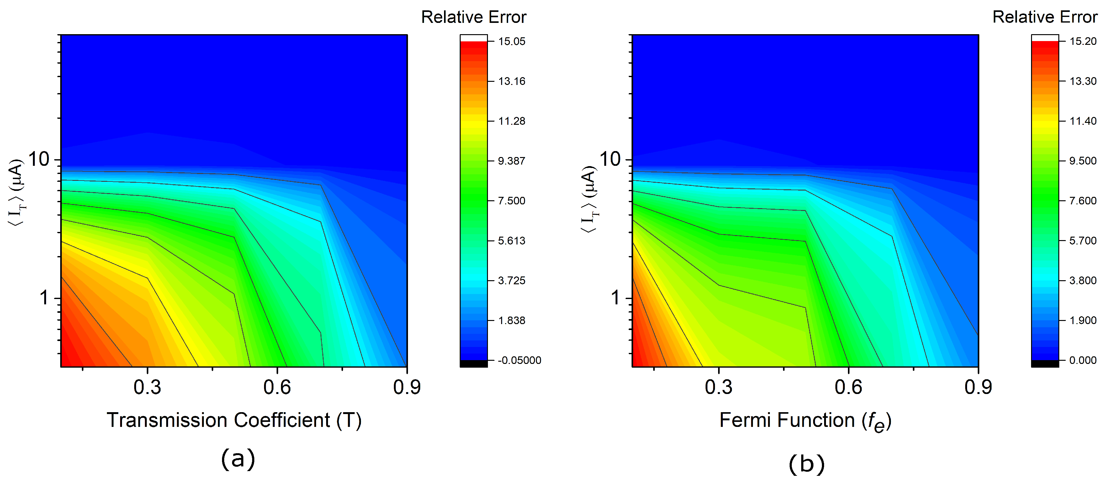
3.2. Numerical Results

In this subsection, to show how the quantum uncertainty of the values of the measured electrical currents can be controlled, we compute the autocorrelation function of the current I T defined as:
I T ( t 2 ) I T ( t 1 ) = d I T k d I T ω I T k I T ω P ( I T k , I T ω ) ,
where P ( I T k , I T ω ) is the probability associated with the subsequent measurement of the multiparticle state | Ψ T at two times t 1 and t 2 > t 1 , with I T ω and I T k defined as the output values of the current at times t 1 and t 2 , respectively.
As indicated in the previous section, for practical reasons in the computation of the particle and displacement components of the current, we will use a wave function plus a Bohmian trajectory for each electron in the computation of the dispersion of I T in the modified quantum device through expressions in Equations (7) and (8). The measurement of the current in an electrical device is a weak measurement process [8] in the sense that the perturbation of the wave function due to the measurement process is not very dramatic. This type of measurement is mathematically represented by three subsystems: the quantum system, the measuring apparatus plus an intermediate system or ancilla. In fact, the system interacts with the ancilla during the measurement (not with the apparatus) and the apparatus measures the ancilla (not the system). This indirect way of getting information of the system by measuring the ancilla implying that the output value of the total current has the quantum noise of the system plus the quantum noise of the ancilla. In our particular example, the ancilla is just the cable (in fact there are a very large number of electrons) connecting the RTD with the ammeter [8]. As indicated in the previous section, for practical reasons in the computation of the particle and displacement components, in addition to the wave function, each electron will be described by a Bohmian trajectory.
As we have mentioned, the elimination of the quantum uncertainty in the measured current implies that the total wave function in Equation (1) is an eigenstate of the many-particle operator in Equation (2). Then, the first measured value of the current I T ( t 1 ) at time t 1 has no influence on the output of a second measurement I T ( t 2 ) at time t 2 , and it can be shown [17] that the two time probability of the autocorrelation given in Equation (9) can be written as the product of two independent probabilities, which leads to the following expression of the two time correlation in Equation (9),
I T ( t 2 ) I T ( t 1 ) = d I T k d I T ω I T k I T ω P ( I T k ) P ( I T ω )
= d I T k I T k P ( I T k ) d I T ω I T ω P ( I T ω )
= I T ( t 2 ) I T ( t 1 )
The condition in Equation (11) is a test of the fact that the quantum uncertainty has disappeared in the measurement process of the modified device. Please note that from a pure engineering point of view, the autocorrelation mentioned above contains rich information on the high frequency response of the quantum device. In order to get the frequency response of the device we compute the power spectral density which is just the Fourier transform of the autocorrelation function (since the current signal has a constant mean, it is in a wide sense a stationary process, hence the auto-correlation depends only on the time difference t = t 2 t 1 . Therefore the auto-correlation function and the PSD form a Fourier transform pair). We therefore define the power spectral density due to the unmodified system, i.e., the system where the protocol is not applied, as P u n m o d i f i e d = F { I T ( t 2 ) I T ( t 1 ) } while P m o d i f i e d = F { I T ( t 2 ) I T ( t 1 ) } for the modified system where the protocol is implemented. Here F represents the Fourier transform operator. Finally we can define the relative error (RE) as:
RE = P m o d i f i e d P u n m o d i f i e d P m o d i f i e d ,
which is plotted in Figure 3. The RE in Equation (12) contains quantum noise at all frequencies. Since all electrical devices are, in fact, a low pass filter, it is interesting for engineering purposes to quantify the error as a function of the frequency. A value of the RE equal to zero indicates that the quantum uncertainty (of the system and ancilla) has been eliminated which has a direct correspondence with the increase in the transport electrons in the device that can be further attributed to a large transmission or a large average current. Besides this it is also easy to see that to arrive at a zero quantum uncertainty we do not need an infinite number of electrons.
In our simulation the total number of electrons injected is given by N = t / τ i n where t is the total simulation time (the time after which the mean current reaches a constant value) and τ i n is the injection time of electrons. Now we know that I T = q T f e τ i n where T is the transmission coefficient and f e is the Fermi function which we assume to be unity. So it is straightforward to see that N = t I T q T f e . We used the total time of simulation as 50 ps, T = 0.7 , f e = 1 and I T = 5 μ A. These values correspond to a point in graph where the uncertainty starts to disappear which gives us the value of N 2232 . Which is a large value but not infinite.

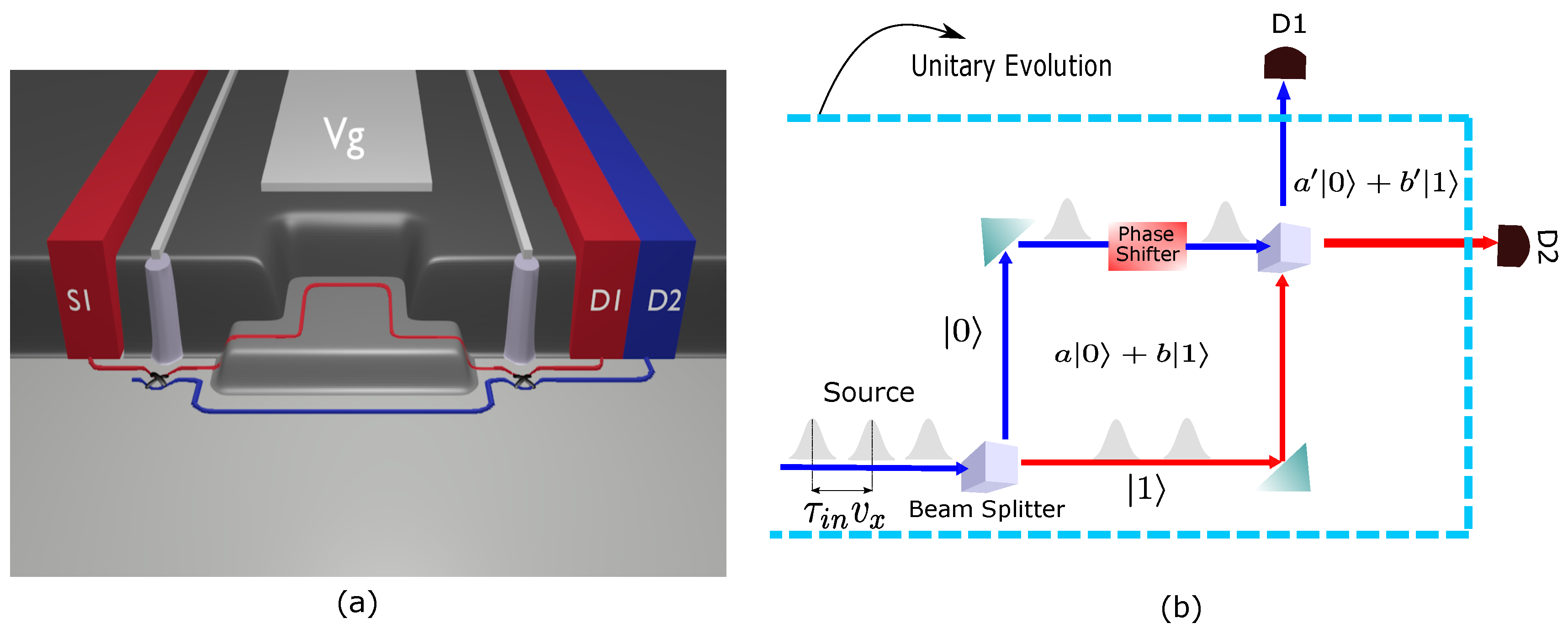
4. Application to Quantum Computing Devices: Mach-Zehnder Interferometer

We provide now an example of our protocol for reducing the quantum uncertainty in a quantum computing device. Quantum computing algorithms require a suitable set of quantum gates to reproduce logical operations [18,19,20]. With respect to most recent implementations, mainly based on superconducting [21] or single-ion qubits [22], solid-state devices are promising candidates because of their scalability and potential to be integrated into classical circuitry. In this section we will study how the quantum uncertainty can be eliminated in a solid-state MZI acting as quantum gate.
It is important to notice that any practical implementation of a quantum gate tends to have a non-negligible interaction between the quantum system and the environment (in terms of scattering with photons, background charges, impurities etc.) even when no measurement is designed. This interaction affects the expected unitary evolution of the state of the quantum system and produces loss of the logical information encoded in the state (decoherence). In solid-state MZI proposal, decoherence can be successfully minimized by injected electrons in edge states, chiral conductive channels generated in the Integer Quantum Hall regime [23]. Then, a strong enough magnetic field B is applied perpendicularly to a 2DEG, so that the band structure is discretized into Landau levels. In proximity to the confining potential of the device, the system eigenstates form chiral channels where an electron propagates coherently for large distances [24]. The chirality of such edge states prevents the electron to be back-reflected by eventual impurities on its path, unless it is scattered to the counterpropagating edge channel by a narrow quantum point contact [25,26]. Coherent transport of electrons in edge states has been tested in a large variety of semiconductor devices, as Fabry-Perot interferometers [27], Hanbury-Brown-Twiss [28] and Hong-Ou-Mandel interferometers [29], thus validating the Integer Quantum Hall regime as an ideal framework to implement solid-state quantum logic gates [30].
Our MZI is schematically depicted in Figure 4. To simplify the discussion, as done along the whole paper, only one degree of freedom (one qubit) is considered for the unmodified quantum device. The generalization of the present protocol to a realistic quantum computing gate with more qubits, is explained in Appendix A. We consider that a contact or reservoir (as elaborated in Appendix B) is connected to the source contact (S1) in Figure 4a filling only one Landau level and all injected electrons have the same wave function | 0 , but displaced in time by the distance τ i n v x , as depicted in Figure 4b. At this point, we have not yet constructed the superposition of states to get our initial qubit. In our device setup, a potential dip or a quantum point contact acts as a half-reflecting beam splitter by randomly scattering the electron in one of the two available edge channels [31,32,33] so that the description of the quantum electron in the central region of our MZI is given by the quantum bit a | 0 + b | 1 . This conclude the first step of the preparation of the quantum state. Then, a tunable potential mesa generated by top gates further separates the two quantum rails, so that the traveling electron accumulates a different phase according to its path [34] as shown in Figure 4a. The two electron beams are then recollected at the second beam splitter to produce the electron interference which is the second step in a quantum device for the (unitary) manipulation of our initial quantum logical information. The final step is the measuring of the observable associated with the final qubit a | 0 + b | 1 by the detectors D 1 and D 2 in Figure 4. As in the case of the RTD, typically the electrical current (which is proportional to the transmission probability from source i = 1 to detector j = 1 , 2 ) is used to indirectly identify the final qubit [35].
The magnetically dependent transmission probability T 21 ( B ) for an electron in the input channel S1 to be detected at D2 can be analytically computed by means of a simplified 1D model based on the scattering matrix approach, as in Ref. [34] and reads:
T 21 ( B ) = 2 T ( 1 T ) ( 1 + cos ( Φ ) ) ,
where T is the transmission coefficient of the single beam splitter and Φ is the total phase difference accumulated in the MZI:
Φ = q B A + φ .
Aharonov-Bohm oscillations in the transmission amplitude [36] are then driven by a variation of the magnetic field B or the loop area A , affecting the phase Φ . This platform can be used to implement other electron interferometry schemes for single electrons, e.g., Fabry-Perot geometries [27], or two interacting electrons [31,37,38]. Let us notice that the consideration of more qubits in the unmodified quantum device will just require occupying different Landau levels, but the basic understanding of how the uncertainty in the measurement can be controlled will not be modified by the presence of more qubits.

4.1. Implementation of Condition 1 and Condition 2

As with Section 3, here too we ensure that our modified quantum device satisfies the conditions mentioned in Section 2.2. Here condition 1 can be obtained with a different strategy than the one used for the RTD since electrons are entering in the MZI one by one (as in a quantum wire). The strategy is enlarging the length L of the arms of the active region of the device (between S 1 and D 1 , D 2 ) to increase the number of simultaneous single particle wave packets that fit inside the device. We argue in the Appendix B that a natural way in the injection of electrons from the contacts in the device is at time intervals τ i n , as defined in Equation (A8) in Appendix B. Neglecting the thermal noise of the contacts the spatial separation between electrons is therefore given by τ i n v x as plotted in Figure 4. Notice that such spatial separation ensures that the consideration of non-interacting electrons required in Equation (1) is more accurate for our modified MZI than for the RTD mentioned before.
As indicated in Appendix C, the consideration of metallic contacts with a lateral area A satisfying A L is necessary condition to be able to successfully use Equation (7) in the computation of the experimental current. Notice that enlarging the lateral area A does not imply an increment of the number N of electrons here since electrons can only enter inside the device, one by one, in the 1D edge channels. Besides this condition 2 can again be obtained by post-processing the experimental current I e x p as indicated in Section 3, by fixing the total time T that we allow the electrons to enter inside the enlarged active device region, N = T / τ i n .

4.2. Numerical Results

To prove the discussions in the previous sections numerically we implemented the Mach-Zehnder like behaviour in the simulations. We were able to attain the Aharonov-Bohm oscillations where the maximum and the minimum value of the current obtained in one of the drains of the MZI oscillates with the change in the magnetic field (see Figure 5a). These oscillations are a signature of the correct working of our simulations. As expected, we observe that the instantaneous current I T ( t ) computed in the quantum device with a large number of electrons is much less noisy than the ones with fewer electrons, as plotted in Figure 5b. The noise in the current value due to fewer electrons results in very high fluctuations in the instantaneous value (black line in Figure 5b) which forces the experimenter to record the values in several experiments to finally get an ensemble value which is non-fluctuating. However, with the successful application of our protocol the fluctuation of the instantaneous value of the current almost disappears (cyan line in Figure 5b) as a result one needs to make just one measurement to get the correct value of the current. The final step of this protocol is determining the value of N which as discussed above can be given by N = T / τ i n .

5. Conclusions

The measured current associated with a quantum device with few electrons has a quantum uncertainty due to the intrinsic stochastic process of the quantum measurement of the electrical current. From an engineering point of view, this quantum uncertainty becomes an undesired quantum noise that makes the discrimination of the final state in classical or quantum gates more difficult. To avoid the quantum uncertainty in the evaluation of the output value, one usually repeats the measurement at different time (using ergodic arguments) to compute a time-averaged value free from uncertainties. We have presented in this paper a new protocol that modifies the original quantum electron device to accommodate a larger number of electrons inside, so that the total electrical current of the modified device (when normalized to the number of electrons inside) gives the value of the output current without quantum uncertainty. We provide numerical examples for classical and quantum computing, with an RTD and MZI, respectively. We demonstrate that the many-particle wave function associated with the modified device is, in fact, an eigenstate of the many-particle electrical current operator. The similitude and differences of our protocol with the collective measurements is mentioned in the text. The results of our protocol can be alternatively understood as a consequence of the central limit theorem (see Appendix E). Although the assumption of non-interacting quasi-particles can seem reasonable in nanoscale electron devices, further work is needed to check whether or not the presence of strong Coulomb and exchange correlations among electrons located inside the device can affect the present predictions. In addition, the discussion on the advantages of the protocol presented here needs to be explored for the quantum measurements of transient currents and delay time of classical and quantum gates.

Author Contributions

Conceptualization, D.P., L.B., M.V., G.A., P.B., A.B. and X.O.; Formal analysis, D.P., L.B., M.V., G.A., P.B., A.B. and X.O.; Investigation, D.P., L.B., M.V., G.A., P.B., A.B. and X.O.; Methodology, D.P., L.B., G.A., P.B., A.B. and X.O.; Software, D.P., L.B., M.V., G.A., P.B., A.B. and X.O.; Supervision, G.A. and X.O.; Validation, D.P., L.B., M.V., G.A., P.B., A.B. and X.O.; Visualization, D.P., L.B., M.V. and X.O.; Writing—original draft, D.P., L.B., M.V., G.A., P.B., A.B. and X.O.; Writing—review and editing, D.P., L.B., M.V., G.A., P.B., A.B. and X.O.

Acknowledgments

The authors acknowledge funding from Fondo Europeo de Desarrollo Regional (FEDER), the “Ministerio de Ciencia e Innovación” through the Spanish Project TEC2015-67462-C2-1-R, the European Union’s Horizon 2020 research and innovation programme under grant agreement No Graphene Core2 785219 and under the Marie Skłodowska-Curie grant agreement No 765426 (TeraApps), and the EC Research Innovation Action under the H2020 for the Project HPC-EUROPA3 (INFRAIA-2016-1-730897), together with the support provided by Barcelona Supercomputing Center (project HPC17D8XLY).

Conflicts of Interest

The authors declare no conflict of interest.The funders had no role in the design of the study; in the collection, analyses, or interpretation of data; in the writing of the manuscript, or in the decision to publish the results’.

Appendix A. Generalization to an Unmodified Quantum Device with Many Electrons

In the text, to simplify the notation and the discussion of our protocol, we have assumed that the unmodified (original) quantum device has only one electron in the active region.This assumption is obviously unrealistic in many scenarios for either classical or quantum computing. For example, in quantum computing, we need a nanoscale devices with, at least, the number of electrons equal to the number of qubits we want to deal with. We show in this appendix that the very same protocol described in the text for one electron can be straightforwardly generalized to deal with an unmodified (original) quantum device with many electrons present in the active region of the nanoscale device.
We consider an unmodified (original) quantum device with M electrons in the active region. To simplify the discussion, we will write the quantum state in the position representation. Then, each electron is described by the degree of freedom x j with j = 1 , 2 , , M . Such quantum system is described by the M-particle wave function:
ψ ( x 1 , x 2 , , x M , t i n )
Notice that we do not assume any particular shape of this M-particle wave function so that exchange and Coulomb interaction among the M electrons is taken into account in the definition of this M-particle system (without any restriction).
Now, we consider N set of M electrons which are prepared under the same conditions as the ones in Equation (A1). In other words, the quantum dynamics of each set of these M electrons can be described by the same wave function in Equation (A1). Thus, we define N × M degrees of freedom for the modified quantum device as x j i with i = 1 , 2 , , N counting the repetitions and j = 1 , 2 , , M counting the number of electrons in each repetition. We define N wave function identical to Equation (A1), but with a superindex i = 1 , 2 , , N indicating which is the repetition we are dealing with:
ψ i ( x 1 i , x 2 i , , x M i , t i n )
Introducing the wave function in Equation (A2) into the quantum state of the modified quantum device written in Equation (1), in the position representation, we have:
Ψ T ( x 1 1 , x M N , t i n ) = ψ 1 ( x 1 1 , , x M 1 , t i n ) · ψ 2 ( x 1 2 , , x M 2 , t i n ) · . · ψ N ( x 1 N , , x M N , t i n )
Clearly, we have assumed in our definition of Ψ T ( x 1 1 , x M N , t i n ) in Equation (A3) that there is no Coulomb or exchange interaction between the subset of electrons { x 1 k , , x M k } (for a treatment of the effect of exchange interaction see Appendix D) and the subset of electrons { x 1 l , , x M l } for any j k , but no restriction is imposed on the interaction among the M electrons of each subset. The rest of the demonstration till the final result in Equation (6) with σ I T 2 = 0 are basically the same that we wrote in Equations (3)–(5) for the evaluation of mean values.
A relevant point in our discussion is that even with our best technological means to exactly reproduce the same wave function in Equation (A1) with another set of M electrons, the quantum dynamics of these new set of electrons is not exactly identical to the previous one because of the inherent quantum uncertainty. The key element in our demonstration is that all these N different uncertainties of the set of M electrons have to follow an identical probability distribution given by the same wave function ψ in Equation (A1).
We notice that we have discussed in this appendix that if a system of N × M electrons are described by Equation (A3) (what we call condition 1 in the text) and if we use a (center-of-mass-type) operator in Equation (2) (what we called condition 2 in the text), then, the uncertainty in the measurement disappears in the lim N . A different question is how to ensure that a modified quantum device is effectively described by Equation (A3) and the measurement by the operator in Equation (2). This last point is what we discussed in detail in the implementations of our protocol with a RTD and a MZI in the text.
Finally, let us notice that the results in this appendix can be understood in a quite different way. It can be used to justify that some amount of Coulomb interaction (between nearest neighbors) can be accepted between the different N subsets. Let us consider again an unmodified system with only one electron described by the wave function ψ ( x 1 , t i n ) . Let us consider that some of the electrons of the N subsets (not all) do have interaction among them. We define M as the number of electrons that have interaction among them (for example we can consider two-electron interaction, but neglect three-electron interaction). Then, the wave function that define these interacting electrons is ψ i ( x 1 i , x 2 i , , x M i , t i n ) . If we assume that the (normalized to the number of electrons) probability distribution of the electrical current assigned to ψ i ( x 1 i , x 2 i , , x M i , t i n ) is not much different than the probability distribution of the electrical current assigned to ψ ( x 1 , t i n ) , then, the demonstration in this appendix can be used to justify that our protocol can be reasonably valid when some interaction is accepted between nearest neighbors { x 1 k , , x M k } and { x 1 l , , x M l } .

Appendix B. The Injection Time

The phase space density of electrons in a reservoir can be anticipated by assuming that each degree of freedom of an electron needs a phase space area equal to 2 π , which is usually derived by using the single particle wavefunction of electrons as the Bloch states and then introducing the Born-von Karman boundary conditions. The interpretation of this result for two wave packets with spatial dispersion σ x and wave vector dispersion σ k = 1 / σ x , center positions x 01 and x 02 , and center wave packets k 01 and k 02 is simple. When they are far away from each other in the phase space, i.e., | x o 1 x o 2 | > > σ x or | k o 1 k o 2 | > > σ k , the norm of the two-electron wave function is equal to the unity. However, when the wave packets are approaching each other, the probability decreases. In particular, for x o 1 = x o 2 and k o 1 = k o 2 , we get ψ 1 ( x ) = ψ 2 ( x ) and Φ ( x 1 , x 2 ) = ψ 1 ( x 1 ) ψ 1 ( x 2 ) ψ 1 ( x 2 ) ψ 1 ( x 1 ) = 0 . This is the time-dependent wave packet version of the Pauli exclusion principle (or exchange interaction) mentioned for time-independent Hamiltonian eigenstates.
For example, for electrons in a 2D space (with the position r = { x , y } and wave vector k = { k x , k y } ), we consider a volume of the phase space equal to Δ x Δ z Δ k x Δ k z , with the degrees of freedom { x 0 , z 0 , k x , k z } satisfying x 0 < x < x 0 + Δ x , z 0 < z < z 0 + Δ z , k x 0 < k x < k x 0 + Δ k x and k z 0 < k z < k z 0 + Δ k z . The total number of electrons in this phase space cell taking into account the properties of a fermion are,
n p = Δ x Δ z Δ k x Δ k z ( 2 π ) 2 ,
where ( 2 π ) 2 is the volume occupied by a single electron in the 2D phase space. Then, the time of injection of an electrons in the x direction from this volume of the phase space will be given by:
τ i n = Δ x v x n p = ( 2 π ) 2 1 v x Δ z Δ k x Δ k z ,
where v x is the electron velocity in the phase space volume. It can be demonstrated [39] that interpretation of Δ x and Δ k x in terms of the wave packets mentioned above implies:
Δ x = σ x 2 π ,
Δ k x = σ k 2 π .
We notice that the condition σ x · σ k = 1 implies the desired condition Δ x · Δ k x = 2 π . Then, the injection time in Equation (A5) is just:
τ i n = σ x v x ,
which only depends on the properties of the reservoir.

Appendix C. Description of the Current Signal and Condition 2

We discuss here which are the necessary considerations to design the modified (new) quantum device that allows us to assume that all electrons inside it have identical simultaneous contribution to the total current I T .
The first step is identifying the proper single particle operator I ^ 1 . Then, once we identify I ^ 1 , we can compute the eigenstates | ψ 1 ( t i n ) and the eigenvalues I 1 that will correspond to the measured output results. However, identifying the electrical current operator is not so simple for several reasons. First, the measured current in an ammeter at time t i n is not just the particle current, defined as the number of particles crossing a particular surface of the device, but it also includes the displacement current. The latter component of the electrical current is proportional to the time-dependent variations of the electric field on a particular surface of the device. Typically, such component is not relevant at low frequencies, but at larger frequencies no instantaneous current conservation at time t i n can be guaranteed without it. What is the operator associated with the measurement of the total, particle plus displacement, current? The answer is not trivial at all. In fact, the measurement of the electrical current in quantum electron devices has an additional difficulty. The measurement of the electrical current corresponds to a generalized or weak measurement, which are mathematically described by a POVM. So, the proper question is even more complicated now: What is the POVM associated with the measurement of the total, particle plus displacement, current?
Fortunately, we can describe the measurement of the total electrical current in a quantum electron device without having to anticipate the POVM. We will use in this appendix an explanation of the measurement process of the total electrical current using the Bohmian quantum theory. Such theory is formally equivalent to the orthodox quantum theory, it gives the same empirical results, but it does not require to identify a priori the measurement operator. Such theory defines a quantum system assigned to one electron by the orthodox wave function ψ 1 ( r , t ) plus a quantum trajectory r 1 ( t ) = { x 1 ( t ) , y 1 ( t ) , z 1 ( t ) } constructed from a velocity field given by the wave function itself. Such trajectory allows the definition of the properties of a quantum system, like the instantaneous electrical current I 1 ( t ) , independently of the fact of being measured or not. An identically prepared state for a second experiment will be described by the same wave function ψ 2 ( r , t ) = ψ 1 ( r , t ) , but with a different trajectory r 2 ( t ) = { x 2 ( t ) , y 2 ( t ) , z 2 ( t ) } . The quantum uncertainty in the output value of the electrical current is due to the different initial positions of the trajectories, which describe an ensemble of identical experiments. The selection of the initial positions of the i-th trajectories is selected according to the quantum equilibrium [40].
According to the Bohmian theory, for the electron with trajectory r 1 ( t ) = { x 1 ( t ) , y 1 ( t ) , z 1 ( t ) } and velocity v 1 ( t ) = { v x 1 ( t ) , v y 1 ( t ) , v z 1 ( t ) } , the electrical (particle plus displacement) current I 1 ( t ) generated in a surface of the quantum device is given by the Ramo-Shockley-Pellegrini theorem [41]. If we assume that each dimension of the lateral contact area A of the quantum device is much larger than the length L between contacts (from source to drain), i.e., A L , and this contacts are ideal metals (with an instantaneous screening time), then the total current generated by an electron crossing the device between the metals is given by the expression:
I 1 ( t ) = q v x 1 ( t ) L [ Θ ( t t i n 1 ) Θ ( t o u t 1 t ) ] ,
where Θ ( t ) is the Heaviside function representing the time dependence of the single electron current pulse with t i n 1 and t o u t 1 = t i n 1 + t r being the entering and leaving times, respectively, and t r is the electron transit time. The pulse starts when the electron enters the device and ends when the electron leaves it. We notice that the integration in time of Equation (A9), during the time interval L / v x , gives the fundamental electron charge t i n 1 t o u t 1 I ( t ) d t = q .
As discussed in the Appendix B, we do not have a perfect control on the preparation of the electrons leaving the contacts and entering inside the device but, assuming the contact to be in (quasi) thermodynamic equilibrium we can anticipate the energy distribution of the injected electrons (Fermi-Dirac distribution) and the interval time between consecutive injection of electrons. The total (particle plus displacement) instantaneous current I e x p of the device is then given by:
I e x p ( t ) = i = 1 N ( t ) I i ( t ) = i = 1 N ( t ) q v x i ( t ) L ,
where N ( t ) is the number of electrons inside the device at time t. Expression (A10) has the desired property that the current due to all electrons inside the device is just the sum of currents due to individual electrons. Notice, however, that I e x p in terms of Bohmian currents is not exactly equal to the I T defined in Equation (2) reinterpreted in terms of Bohmian currents, because a factor N in the denominator of Equation (2) is missing in Equation (A10).
Finally, we emphasize that the Bohmian trajectories have been introduced in this last part just to simplify our practical discussion about the measurement of the total (particle plus displacement) current in quantum electron devices, but it has no fundamental role in the demonstration of the proposed protocol. In other words, the validity of the main result in Equation (6) can be equivalently demonstrated with orthodox quantum mechanics (as we have done) or with Bohmian quantum mechanics. The knowledge that we gain from the Bohmian development done here is that the total (particle plus displacement) current measured in experiments do satisfy the required superposition of currents associated with individual electrons and that a factor N ( t ) has to be added into the experimentally measured current of the modified quantum device I e x p to properly define I T as I T ( t ) = I e x p ( t ) N ( t ) where two proper ways of computing N ( t ) are explained in the RTD and MZI applications mentioned in th text.

Appendix C.1. On the Assumption of a Large Lateral Area in the Active Region

The size of the lateral area A is a very important point in our protocol since we want that each electron inside the device active region contribute to the measured electrical current. If the electrical current were only due to the particle (conduction) current component, then, only the electrons crossing the drain (or source) surface, would have contributed to the current. However, it is well known that the electrical current is due to both particle and displacement currents. In fact, an electron far from the drain surface can still affect the current if its dynamics generates a significant perturbation in the electric field. If the lateral area is large compared to the longitudinal ones i.e., A L , then, effectively all electrons inside the active device region can contribute to the measured current, as required by the operator in Equation (2). The formal derivation of this issue is presented in Ref. [8]. Thus, the large lateral area is an important point of our protocol.
Only when L W , H , then, one can ensure that all electrons are equally contributing (through the displacement current) to the total current and hence condition 2 in the main text is satisfied.

Appendix C.2. On the Assumption of an Instantaneous Screening Time in the Metallic Contacts

Next we discuss the motivation behind approximating the screening time in the metalic contacts to be instantaneous. The fact that we assume a screening time in the contacts (metals) much smaller than in the active region is something usual in electron semiconductor devices. Typically, the screening time in metals is considered to be negligible in comparison with the screening time in a semiconductor. The implications of this condition is that we do not need to simulate the electrons deep inside the source/drain contact (without entering in the device) generating displacement current in the drain (or source) contact. This is possible only if we assume the screening time in the metals to be (almost) instantaneous.

Appendix D. Effects of Exchange Symmetry on the Total Current Many Body Operator

In the text, we have assumed that the many-particle wave function in Equation (1) has no exchange symmetry. Here, we discuss the physical soundness of such approximation. Let us evaluate the effects of exchange symmetry on the squared total current of Equation (2) for two particle case, which can be rewritten as:
I ^ T 2 = 1 4 i = 1 2 I i I i + 1 4 i = 1 , j i 2 I i I j ,
where indexes i , j refers to the particle with coordinate x i in the phase space. We assume the system wave function described by the two-fermion state with exchange symmetry
Ψ ( x 1 , x 2 ) = 1 2 ( ψ 1 ( x 1 ) ψ 2 ( x 2 ) ψ 2 ( x 1 ) ψ 1 ( x 2 ) ) ,
where the superindex k of the state ψ k refers to the injection time (e.g., ψ 1 is injected at t i n , while ψ 2 is injected at t i n + τ i n ). Within this definition of the state, the diagonal average values of the first value in Equation (A11) read:
I 1 I 1 = 1 4 ( ψ 1 | ( I 1 ) 2 | ψ 1 ψ 2 | ψ 2 + ψ 2 | ψ 2 ψ 1 | ( I 1 ) 2 | ψ 1 ψ 1 | ( I 1 ) 2 | ψ 2 ψ 2 | ψ 1 ψ 2 | ( I 1 ) 2 | ψ 1 ψ 1 | ψ 2 ) ,
for i = 1 , 2 . We reasonably assume an initial negligible overlap of the wave packets,
ψ α | ψ β δ α , β ,
which is conserved during the evolution of the two electrons, carrying out the same procedure for the second diagonal element we get:
I 1 I 1 + I 2 I 2 = 1 2 ( ψ 1 | ( I 1 ) 2 | ψ 1 + ψ 2 | ( I 2 ) 2 | ψ 1 ) ,
as for distinguishable particles. Similarly, the first non-diagonal term of Equation (A11) is computed:
I 1 I 2 = 1 4 ( ψ 1 | I 1 | ψ 1 ψ 2 | I 2 | ψ 2 + ψ 2 | I 1 | ψ 2 ψ 1 | I 2 | ψ 1 ψ 1 | I 1 | ψ 2 ψ 2 | I 2 | ψ 1 ψ 2 | I 1 | ψ 1 ψ 1 | I 2 | ψ 2 ) ,
Computing the same for the second non-diagonal element we get,
I 1 I 2 + I 2 I 1 = 1 2 ψ 1 | I 1 | ψ 1 ψ 2 | I 2 | ψ 2 .
So using Equations (A15) and (A17) in Equation (A11) we get,
I ^ T 2 = 1 4 i = 1 2 I i I i + 1 4 i = 1 , j i 2 I i I j = 1 4 i = 1 2 ( ψ i | ( I i ) 2 | ψ i + 1 4 i = 1 , j i 2 ψ i | I i | ψ i ψ j | I j | ψ j ,
The mean value of the squared of the total current for distinguishable particles is therefore recovered by assuming ψ i | I | ψ j δ i , j . This constraint is fulfilled by Equation (A14), together with the definition of the current operator, which is related to momentum (proportional to a spatial derivative in the real space) and position operators. Indeed, we expect that for a weak measurement of the current discussed in the text, the state | ψ j produced by its application to a wave packet ( | ψ j = I | ψ j ) is characterized by a spatial localization that does not significantly differ from the unperturbed state | ψ j , so that ψ i | I | ψ j 0 is valid.

Appendix E. The Ontological Meaning of the Total Measured Current I ^ T and the Classical Central Limit Theorem

We discuss here a simple interpretation of the main result given in Section 2.2. The ammeter mentioned in the text does only measure the value of the total current I ^ T . Therefore, strictly speaking, the currents I 1 ^ , I 2 ^ , etc. contributed by the single electrons, have not been measured, so the electrons have no (orthodox) definite value of their current. We are invoking here the well known eigenvalue-eigenstate link. The i-th electron has a well-defined value of the current when its wavefunction is an eigenstate of the single particle current operator I i ^ . However as explained in Section 2.1, the single particle state describing the i-th electron is not a current eigenstate. Therefore there is no orthodox value for the current assigned to the i-th electron.
In any case, let us assume that we can assign (unmeasured) values of the current of each electron (for i = 1 , , N ) at any time (The physical correctness of this assumption will be provided below). Thus, the definition of the total current in Equation (2) in terms of operators can be translated into an expression in terms of variables which takes well-defined values:
I T = I 1 + I 2 + . + I N N ,
We eliminate the “hat” in Equation (A19) to clarify that now I i is not an operator, but a variable. Then, assuming again the independence among the variables I i and that the total current can be given by the above sum, the simple application of the classical central limit theorem will be enough to certify that the variance of I T goes to zero when N is large enough.
However, the reader can argue that such simple understanding is not appropriate because, as we emphasized at the beginning of this appendix, the current of each electron has no well-defined value. Such values are not measured by the ammeter and, strictly speaking, the values associated with the current operators I 1 ^ , I 2 ^ are undefined in the orthodox theory.
In any case, the simple understanding based on the central limit theorem, can be invoked by using a quantum theory with a definition of the reality of the properties of electrons independent of the measurement process. This understanding is supported for example from modal interpretation of the quantum world where the reality of some properties of electrons (like its electrical current) has a well-defined value independently of the fact that they are measured or not. This understanding is consistent with our paper where the Bohmian theory [40], which is the most famous modal interpretation today, is invoked for the computation of the currents. At the end of the day, the discussion about the (hidden) reality of the values of the current of each electron are not relevant for the empirical results presented along the work. Bohmian and orthodox theories are empirically equivalent for all known experiments. The above discussion provides a simple and intuitive understanding of the physical soundness of providing a many-body quantum state in Equation (1) with no quantum uncertainty.

References

  1. Le, H.Q.; Van Norstrand, J.A.; Thompto, B.W.; Moreira, J.E.; Nguyen, D.Q.; Hrusecky, D.; Kroener, M. IBM POWER9 processor core. IBM J. Res. Dev. 2018, 62, 2:1–2:12. [Google Scholar] [CrossRef]
  2. Cory, C.D.; Datta, S. Nanoscale transistors—Just around the gate? Science 2013, 341, 140–141. [Google Scholar]
  3. Nielsen, M.A.; Chuang, I.L. Quantum computation. In Quantum Information; Cambridge University Press: Cambridge, UK, 2000. [Google Scholar]
  4. Boixo, S.; Isakov, S.V.; Smelyanskiy, V.N.; Babbush, R.; Ding, N.; Jiang, Z.; Neven, H. Characterizing quantum supremacy in near-term devices. Nat. Phys. 2018, 14, 595. [Google Scholar] [CrossRef]
  5. Classical and quantum computers are vying for superiority. Nature 2018, 564, 302. [CrossRef] [PubMed]
  6. Tang, A.E. Quantum-inspired classical algorithm for recommendation systems. arXiv 2018, arXiv:1807.04271. [Google Scholar]
  7. Deutsch, D. Uncertainty in quantum measurements. Phys. Rev. Lett. 1983, 50, 631. [Google Scholar] [CrossRef]
  8. Marian, D.; Zanghì, N.; Oriols, X. Weak values from displacement currents in multiterminal electron devices. Phys. Rev. Lett. 2016, 116, 110404. [Google Scholar] [CrossRef] [PubMed]
  9. Zhan, Z.; Kuang, X.; Colomés, E.; Pandey, D.; Yuam, S.; Oriols, X. Time-dependent quantum Monte Carlo simulation of electron devices with two-dimensional Dirac materials: A genuine terahertz signature for graphene. Phys. Rev. B 2019, 99, 155412. [Google Scholar] [CrossRef] [Green Version]
  10. Oriols, X.; Benseny, A. Conditions for the classicality of the center of mass of many-particle quantum states. New J. Phys. 2017, 19, 063031. [Google Scholar] [CrossRef] [Green Version]
  11. Lloyd, S.; Slotine, J.J.E. Quantum feedback with weak measurements. Phys. Rev. A 2000, 62, 012307. [Google Scholar] [CrossRef] [Green Version]
  12. Hou, Z.; Tang, J.F.; Shang, J.; Zhu, H.; Li, J.; Yuan, Y.; Wu, K.D.; Xiang, G.Y.; Li, C.F.; Guo, G.C. Deterministic realization of collective measurements via photonic quantum walks. Nat. Commun. 2018, 9, 1414. [Google Scholar] [CrossRef] [PubMed]
  13. Encomendero, J.; Faria, F.A.; Islam, S.M.; Protasenko, V.; Rouvimov, S.; Sensale-Rodriguez, B.; Xing, H.G. New tunneling features in polar III-nitride resonant tunneling diodes. Phys. Rev. X 2017, 7, 041017. [Google Scholar] [CrossRef]
  14. Gaskell, J.; Eaves, L.; Novoselov, K.S.; Mishchenko, A.; Geim, A.K.; Fromhold, T.M.; Greenaway, M.T. Graphene-hexagonal boron nitride resonant tunneling diodes as high-frequency oscillators. Appl. Phys. Lett. 2015, 107, 103105. [Google Scholar] [CrossRef] [Green Version]
  15. Avedillo, M.J.; Quintana, J.M.; Roldán, H.P. Increased Logic Functionality of Clocked Series-Connected RTDS. IEEE Trans. Nanotechnol. 2006, 5, 606–611. [Google Scholar] [CrossRef] [Green Version]
  16. Park, J.; Lee, J.; Yang, K. A 24-GHz Low-Power RTD-Based ON-OFF Keying Oscillator with an RTD Pair Configuration. IEEE Microwave Wirel. Comp. Lett. 2018, 28, 521–523. [Google Scholar] [CrossRef]
  17. Pandey, D.; Albareda, G.; Oriols, X. Measured and unmeasured properties of quantum systems. arXiv 2018, arXiv:1812.10257. [Google Scholar]
  18. Bertoni, A.; Bordone, P.; Brunetti, R.; Jacoboni, C.; Reggiani, S. Quantum Logic Gates based on Coherent Electron Transport in Quantum Wires. Phys. Rev. Lett. 2000, 84, 5912. [Google Scholar] [CrossRef] [PubMed]
  19. Buscemi, F.; Bordone, P.; Bertoni, A. Carrier-carrier entanglement and transport resonances in semiconductor quantum dots. Phys. Rev. B 2007, 76, 195317. [Google Scholar] [CrossRef] [Green Version]
  20. Buscemi, F.; Bordone, P.; Bertoni, A. Quantum teleportation of electrons in quantum wires with surface acoustic waves. Phys. Rev. B 2010, 81, 045312. [Google Scholar] [CrossRef]
  21. Lanting, T.; Przybysz, A.J.; Smirnov, A.Y.; Spedalieri, F.M.; Amin, M.H.; Berkley, A.J.; Dickson, N. Entanglement in a Quantum Annealing Processor. Phys. Rev. X 2014, 4, 021041. [Google Scholar] [CrossRef] [Green Version]
  22. Debnath, S.; Linke, N.M.; Figgatt, C.; Landsman, K.A.; Wright, K.; Monroe, C. Demonstration of a small programmable quantum computer with atomic qubits. Nature 2016, 536, 63–66. [Google Scholar] [CrossRef] [PubMed] [Green Version]
  23. Büttiker, M. Absence of backscattering in the quantum Hall effect in multiprobe conductors. Phys. Rev. B 1988, 38, 9375. [Google Scholar] [CrossRef]
  24. Roulleau, P.; Portier, F.; Roche, P.; Cavanna, A.; Faini, G.; Gennser, U.; Mailly, D. Direct Measurement of the Coherence Length of Edge States in the Integer Quantum Hall Regime. Phys. Rev. Lett. 2008, 100, 126802. [Google Scholar] [CrossRef] [PubMed] [Green Version]
  25. Venturelli, D.; Giovannetti, V.; Taddei, F.; Fazio, R.; Feinberg, D.; Usaj, G.; Balseiro, C.A. Edge channel mixing induced by potential steps in an integer quantum Hall system. Phys. Rev. B 2011, 83, 075315. [Google Scholar] [CrossRef] [Green Version]
  26. Beggi, A.; Bordone, P.; Buscemi, F.; Bertoni, A. Time-dependent simulation and analytical modelling of electronic Mach–Zehnder interferometry with edge-states wave packets. J. Phys.: Condens. Matter 2015, 27, 475301. [Google Scholar] [CrossRef] [PubMed]
  27. Deviatov, E.V.; Lorke, A. Experimental realization of a Fabry-Perot-type interferometer by copropagating edge states in the quantum Hall regime. Phys. Rev. B 2008, 77, 161302. [Google Scholar] [CrossRef] [Green Version]
  28. Neder, I.; Ofek, N.; Chung, Y.; Heiblum, M.; Mahalu, D.; Umansky, V. Interference between two indistinguishable electrons from independent sources. Nature 2007, 448, 333–337. [Google Scholar] [CrossRef]
  29. Bocquillon, E.; Freulon, V.; Berroir, J.M.; Degiovanni, P.; Plaçais, B.; Cavanna, A.; Jin, Y.; Fève, G. Coherence and Indistinguishability of Single Electrons Emitted by Independent Sources. Science 2013, 339, 1054–1057. [Google Scholar] [CrossRef] [Green Version]
  30. Weisz, E.; Choi, H.K.; Sivan, I.; Heiblum, M.; Gefen, Y.; Mahalu, D.; Umansky, V. An electronic quantum eraser. Science 2014, 3444, 1363–1366. [Google Scholar] [CrossRef]
  31. Giovannetti, V.; Taddei, F.; Frustaglia, D.; Fazio, R. Multichannel architecture for electronic quantum Hall interferometry. Phys. Rev. B 2008, 77, 155320. [Google Scholar] [CrossRef] [Green Version]
  32. Karmakar, B.; Venturelli, D.; Chirolli, L.; Giovannetti, V.; Fazio, R.; Roddaro, S.; Pellegrini, V. Nanoscale Mach-Zehnder interferometer with spin-resolved quantum Hall edge states. Phys. Rev. B 2015, 92, 195303. [Google Scholar] [CrossRef] [Green Version]
  33. Bellentani, L.; Beggi, A.; Bordone, P.; Bertoni, A. Dynamics of copropagating edge states in a multichannel Mach-Zender interferometer. J. Phys.: Conf. Ser. 2017, 906, 012027. [Google Scholar] [CrossRef] [Green Version]
  34. Bellentani, L.; Beggi, A.; Bordone, P.; Bertoni, A. Dynamics and Hall-edge-state mixing of localized electrons in a two-channel Mach-Zehnder interferometer. Phys. Rev. B 2018, 97, 205419. [Google Scholar] [CrossRef] [Green Version]
  35. Ji, Y.; Chung, Y.; Sprinzak, D.; Heiblum, M.; Mahalu, D.; Shtrikman, H. An electronic Mach–Zehnder interferometer. Nature 2003, 422, 415. [Google Scholar] [CrossRef] [PubMed]
  36. Bird, J.P.; Ishibashi, K.; Stopa, M.; Aoyagi, Y.; Sugano, T. Coulomb blockade of the Aharonov-Bohm effect in GaAs/AlxGa1 − x As quantum dots. Phys. Rev. B 1994, 50, 14983–14990. [Google Scholar] [CrossRef]
  37. Marian, D.; Colomés, E.; Oriols, X. Time-dependent exchange and tunneling: Detection at the same place of two electrons emitted simultaneously from different sources. J. Phys.: Condens. Matter 2015, 27, 245302. [Google Scholar] [CrossRef]
  38. Bellentani, L.; Bordone, P.; Oriols, X.; Bertoni, A. Coulomb and exchange interaction effects on the exact two-electron dynamics in the Hong-Ou-Mandel interferometer based on Hall edge states. arXiv 2019, arXiv:1903.02581. [Google Scholar]
  39. Oriols, X. Non-universal conductance quantization for long quantum wires: The role of the exchange interaction. Nanotechnology 2004, 15, S167. [Google Scholar] [CrossRef]
  40. Oriols, X.; Mompart, J. Applied Bohmian Mechanics: From Nanoscale Systems to Cosmology; CRC Press: Boca Raton, FL, USA, 2012. [Google Scholar]
  41. Albareda, G.; Traversa, F.L.; Benali, A.; Oriols, X. Computation of quantum electrical currents through the Ramo–Shockley–Pellegrini theorem with trajectories. Fluctuat. Noise Lett. 2012, 11, 1242008. [Google Scholar] [CrossRef]
Figure 1. (a) Schematic of classical computing exemplified with RTD where only the active device is governed by unitary quantum evolutions (enclosed in the cyan color dashed line), while the contacts and the cable leads to quantum decoherence which provides a fixed value of the current obtained in the measuring apparatus (shown at the right end). (b) Schematic of quantum computing exemplified with an MZI where the quantum wholeness require that a coherent unitary evolution appears in all the gates (enclosed in the cyan color dashed line). Only at the end, when the wave function is measured, decoherence can be accepted.
Applsci 09 02300 g001
Figure 2. A 3D schematic of the RTD where the green material represents GaAs while the red represents AlGaAs. The alternating AlGaAs-GaAs-AlGaAs structure results in a potential well with discrete resonant energies.
Applsci 09 02300 g002
Figure 3. (a) Plot between the relative error, the transmission coefficient and the average current with the Fermi function fixed to unity. The relative error which is an indicator of quantum randomness, goes to zero, when the number of electrons in the device quantified by transmission coefficient and the mean current becomes very large (blue shaded region) while the relative probability of error is greater (in the red region) when the number of particles in the device is very small. In the green region the uncertainty already starts to disappear. (b) The same plot but with a constant transmission probability as unity and varying Fermi function also demonstrate the same outcome.
Applsci 09 02300 g003
Figure 4. (a) 3D view of the potential landscape felt by the electrons in the MZI at bulk filling factor 2 in the Integer Quantum Hall regime, in presence of a perpendicular magnetic field [34]. Electrons are injected in the first edge channel by the source S 1 , and collected at the end of the device by the drain D 1 ( D 2 ) . The paths of the electrons in the interferometer is defined by the red (blue) line for the first (second) Landau level. (b) Schematic diagram and functioning of the MZI. Electron injection with non-interacting and non-overlapping wavepackets is shown in gray, while the region encapsulated by the cyan color dashed line box defines the region where the unitary evolution of the quantum states is preserved.
Applsci 09 02300 g004
Figure 5. (a) The Aharonov-Bohm oscillations of the mean current resulting due to the interference of the wavepackets at the output of the Detector 2 oscillating between the maximum and minimum limit of the mean current. (b) The instantaneous current normalized to the number of particles is plotted at the output of the detector 2 of the MZI with respect to the simulation time, for different number of electrons N. As expected, the noise in the current reduces with the increase in the number of transport electrons due to the elimination of quantum uncertainty demonstrating the successful implementation of the protocol discussed in the text.
Applsci 09 02300 g005

