High Performance Asymmetric Coupled Line Balun at Sub-THz Frequency
by
 ,
,
Abdul Ali
1,2,* ,
,
Jongwon Yun
2,3,
Herman Jalli Ng
2,
Dietmar Kissinger
4,
Franco Giannini
1 and
Paolo Colantonio
1
1
Department of Electronics Engineering, University of Rome Tor Vergata, 00133 Rome, Italy
2
IHP—Leibniz-Institut für innovative Mikroelektronik, 15236 Frankfurt (Oder), Germany
3
Samsung Electronics, 18448 Gyeonggi, Korea
4
Institute of Electron Devices and Circuits, Ulm University, 89081 Ulm, Germany
*
Author to whom correspondence should be addressed.
Appl. Sci. 2019, 9(9), 1907; https://doi.org/10.3390/app9091907
Submission received: 2 April 2019
/
Revised: 3 May 2019
/
Accepted: 6 May 2019
/
Published: 9 May 2019
(This article belongs to the Special Issue Millimeter-wave and Terahertz Applications of Metamaterials)
Abstract
:In this paper, we report a high-performance balun with characteristics suitable for future broadband sub-THz differential circuits. The idea of the balun is based on three asymmetric coupled lines, which enhance the odd mode capacitances to equalize the even/odd mode phase velocities. The inner line of the three asymmetric coupled lines is configured to form the open stub (/2), while the outer lines form short stubs (/4). To further reduce the phase imbalance, the short stubs in one of the arms of the balun are connected with vias and a lower metal layer. The balun is developed using the standard 130-nm SiGe BiCMOSback-end process and EM simulated with ADS momentum and Sonnet. The −10-dB reflection coefficient (S) bandwidth of the balun is 136 GHz (88–224 GHz). It shows insertion loss (including RF pads) <1.5 dB, phase imbalance <7 degrees, and amplitude imbalance <1 dB at 94–177 GHz. Furthermore, a scaled-down version of the balun operates on the WR-6, WR-5, and WR-4 frequency bands without significant degradation in its performance. Such characteristics of the balun make it an ideal candidate for various broadband differential circuits.
1. Introduction
With the recent advance in the operating speeds of solid-state devices, high-frequency transistors based on SiGe BiCMOStechnology have been developed with up to 500 GHz [1]. This has allowed the development of various solid-state systems above 100 GHz. These systems have been successfully demonstrated for numerous applications including radar, sensing, radiometric imaging, high-speed wireless communication, and spectroscopy [2,3,4,5,6,7,8,9]. Generally, the basic circuit blocks used in these systems are designed to have fully-differential configurations, which have the advantage of high CMRR (common-mode rejection ratio) for common-mode noise cancellation.
Baluns are essential in constructing differential circuits as they transform single-ended (unbalanced) input signals to differential (balanced) output signals or vice versa [10,11]. They are required in the design and characterization of differential circuits such as voltage-controlled oscillators (VCO), mixers, push-pull amplifiers, and frequency multipliers. Furthermore, single-ended antennas can be connected to differential circuits via a balun. The parameters that assess the performance of a balun are its input/output reflection coefficient, bandwidth, insertion loss, and phase and amplitude imbalance. Depending on the application, any deviation in the balun’s performance from the ideal case can affect the inherent benefits of differential circuits. For instance, in characterizing broadband differential circuits, such as distributed amplifiers or frequency multipliers, the bandwidth of the balun itself must be larger than the circuits. In the case of mixers, the bandwidth, insertions loss, and phase and amplitude imbalance of the balun can directly influence its conversion gain.
Baluns can be broadly divided into active and passive baluns [10,11,12,13,14,15,16,17]. Active baluns have the advantage of a finite gain and occupy a very small area. However, they face linearity issues, which can limit the dynamic range of solid-state circuits. Unlike active baluns, passive baluns do not experiences noise and linearity issues. They can be further classified into lumped element and distributed baluns [14]. The Marchand balun is a type of distributed balun, which exhibits wideband characteristics. Several modifications of the conventional Marchand balun exist in the literature [14,15,16,17,18,19,20]. These modifications have been performed using different technologies (SiGe BiCMOS, CMOS) to improve bandwidth, return loss, reduce the size, and decrease the phase and amplitude imbalance. However, there are still some disadvantages associated with them in terms of limited operational bandwidth, higher losses, or large amplitude and phase imbalances. Furthermore, some of them occupy a larger chip area. Owing to the prominent applications above 100 GHz and the salient features of differential circuits, a broadband balun with minimal losses and amplitude and phase imbalances is highly desired.
Electromagnetic field theory plays a vital role in understanding the behavior of various systems in designing engineered materials and devices for different applications. Recently, electromagnetic field manipulation has been used to design various devices based on metasurfaces, metamaterials, graphene, and plasmonics [21,22,23,24,25,26]. In the field of THz electronics, the electromagnetic field analysis can assist in designing various passive structures such as baluns and power combiners and splitters.
In this work, we report the design of an edged coupled balun based on three asymmetric coupled lines. First, we presented different capacitances associated with coupled lines that control the phase velocities in the even/odd mode. Then, a balun based on three asymmetric coupled lines is designed with IHP’s 130-nm SiGe BiCMOS back-end process to cover the frequency band of 110–220 GHz. The three asymmetric coupled transmission lines increase odd mode capacitances, which improves the balun’s performance parameters. This paper is organized in the following sections. Section 2 presents the theoretical background of the balun. Then, in Section 3, the design and simulation results of the balun are discussed. Finally, Section 4 presents the conclusion and future aspects of the balun.
2. Theoretical Background
The conventional Marchand balun is a three-port network, which consists of a /2 section and two identical /4 sections. The principle operation of the balun relies on electromagnetic coupling between a /2 open/short stub and two /4 short/open stubs. It can be design using even/odd mode analysis of symmetric coupled transmission lines. The parameters that are important in its design are even/odd mode impedances (, ) and the electrical lengths of the coupled lines. Figure 1 shows coupled lines with ports’ assignment (a) and the Marchand balun (b). The corresponding admittance matrix of Figure 1a is given by [27,28],
If a homogeneous medium is considered for the coupled lines, then, under even and odd mode excitations, one can obtain the following equations,
If = 90° (/4), then Equation (2) can be further simplified to,
The conditions for ideal balun operations are,
Using Figure 1b and Equations (3) and (4), one can obtain the following design equations for the balun,
where the subscript x stands for odd or even mode excitation, is the characteristic impedance of the coupled line, is the phase velocity, is the effective dielectric constant, and c is the speed of light in a vacuum. The capacitance can be further expended using Figure 2.
where , , , , and are the parallel plate capacitance, fringing capacitance, gap capacitance in air, gap capacitance in a dielectric, and fringing capacitance in even mode, respectively. Equation (5) is valid if = 90, which requires even/odd mode phase velocities to be equal [20]. It also shows that the large even/odd mode characteristic impedance ratio is required for the design of the balun, which can result in low phase and amplitude imbalance. The ratio can be increased either by decreasing the odd mode impedance or increasing even mode impedance. The odd mode impedance can be decreased if the odd mode capacitances shown in Figure 2 are increased. Using three asymmetric coupled lines, the odd mode capacitances increase by almost twice the two coupled lines, which helps in equalizing the even/odd mode phase velocities. Thus, it can result in low phase and amplitude imbalance over a wide bandwidth.
A strong capacitive coupling is required for an edged coupled balun to have excellent performance, which is proportional to the dielectric material and the area of the coupled lines and inversely proportional to the gap separation between them. The coupling can be enhanced if either the lines are placed very close to each other or lines with a large area and a material with a high dielectric constant are used. However, the standard technologies such as 130-nm SiGe BiCMOS have some limitations in terms of minimum separation between two conductors, and they must be separated by some distance. Additionally, the dielectric constant of the material and thickness of the conductors (which in the case of edge coupling, defines the area of the conductors) are fixed. This makes the design of a wideband edged coupled balun based on two lines highly challenging. Alternatively, three asymmetric coupled lines can be used to design the edged coupled balun, which can assist in attaining the capacitive coupling needed for wideband performance without violating the design rules of standard technologies. The coupling between asymmetric coupled lines can be adjusted with two different sizes of gap separation. The two gaps together with the width of the coupled lines provide extra design flexibility in controlling the even/odd mode capacitances (see Equation (7)).
3. Design of the Asymmetric Coupled Line Balun
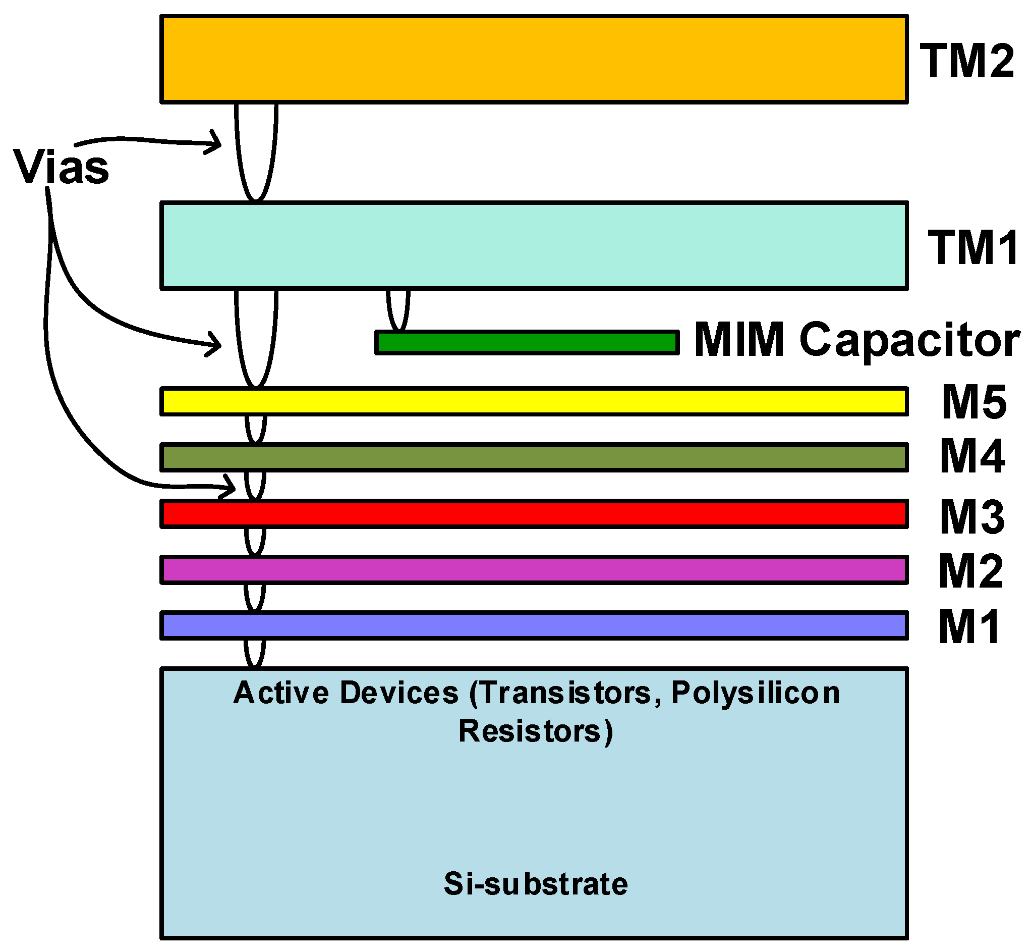
Figure 3 shows IHP’s 130-nm SiGe BiCMOS back-end of the line (BEOL) process cross-section [1,29,30]. The BEOL contains six metal layers including two thick low-loss metals (TM2and TM1), which provide flexibility in choosing different metal layers for the balun design. To design an edged coupled balun, one can use either lower metals (M1–M5) or top metals (TM2, TM1). The TM2 and TM1 have a thickness of 3 m and 2 m, respectively, while the lower metals have a thickness of roughly 0.49 m. In edge-coupling where the thickness of conductors defines the area of the parallel plate, TM2 and TM1, respectively, will give six- and four-times higher coupling than lower metals. This makes the lower metal not suitable to achieve strong mutual capacitive coupling in odd mode. Furthermore, they can increase the insertion loss. Therefore, TM2 and TM1 were utilized in the design of three asymmetric coupled lines, while M3 served as a ground plane.
Figure 4 shows the 3D views of the conventional edged coupled balun (a) and the three asymmetric coupled line balun (b). In the three asymmetric coupled line balun, the inner (/2) line is surrounded by two (/4) lines. The widths (W1, W2) of the lines and separations (S1, S2) among them can be adjusted to increase effective odd mode capacitance as discussed earlier. This helps in equalizing the phase velocities for even and odd mode. In order to match the single-ended input impedance () to 50 and differential output impedance () to 100 , the parameters (W1, W2, S1, and S2) were determined through the parametric study of bandwidth, return loss, insertion loss and the phase and amplitude imbalance of the balun. For instance, Figure 5 shows the effect of S1 and S2 on the input reflection coefficient (), bandwidth, insertion loss, amplitude imbalance, and phase difference of the asymmetric coupled line balun when all three ports were terminated in 50 except for the insertion loss, which was found by placing two baluns in a back-to-back configuration. As can be seen, lower values of S1 and S2 provided a wider bandwidth (Figure 5a,b) and a small amplitude imbalance (Figure 5c,d). However, the matching at the intermediate frequencies was not better than −15 dB, which caused higher mismatch losses (Figure 5e,f) and a phase difference (Figure 5g,h) less than 170 degrees (phase error ≥10 degrees). On the other hand, higher values of S1 and S2 enhanced the matching at the intermediate frequencies, which resulted in lower losses and phase error at a narrow bandwidth. The variation of S1 and S2 changed the even/odd capacitances discussed earlier (see Figure 2). Therefore, intermediate values can be selected, which provide a wider bandwidth with lower losses and amplitude and phase imbalance. A similar study can be performed on W1 and W2. The optimal values for the parameters of the balun were W1 = 5 m, W2 = 6.5 m, S1 = 2.75 m, and S2 = 4.75 m. The length of the /2 and /4 sections were adjusted around the center frequency () of 150 GHz. Furthermore, two adjustment lines made of top metal (TM1) were added in the second arm of the balun where the /2 was terminated in open circuit. These lines increased the length of the second arm slightly to decrease the phase imbalance without affecting the amplitude imbalance. A folded layout was used for the balun to reduce its size, which resulted in a small area of 0.0318 mm.
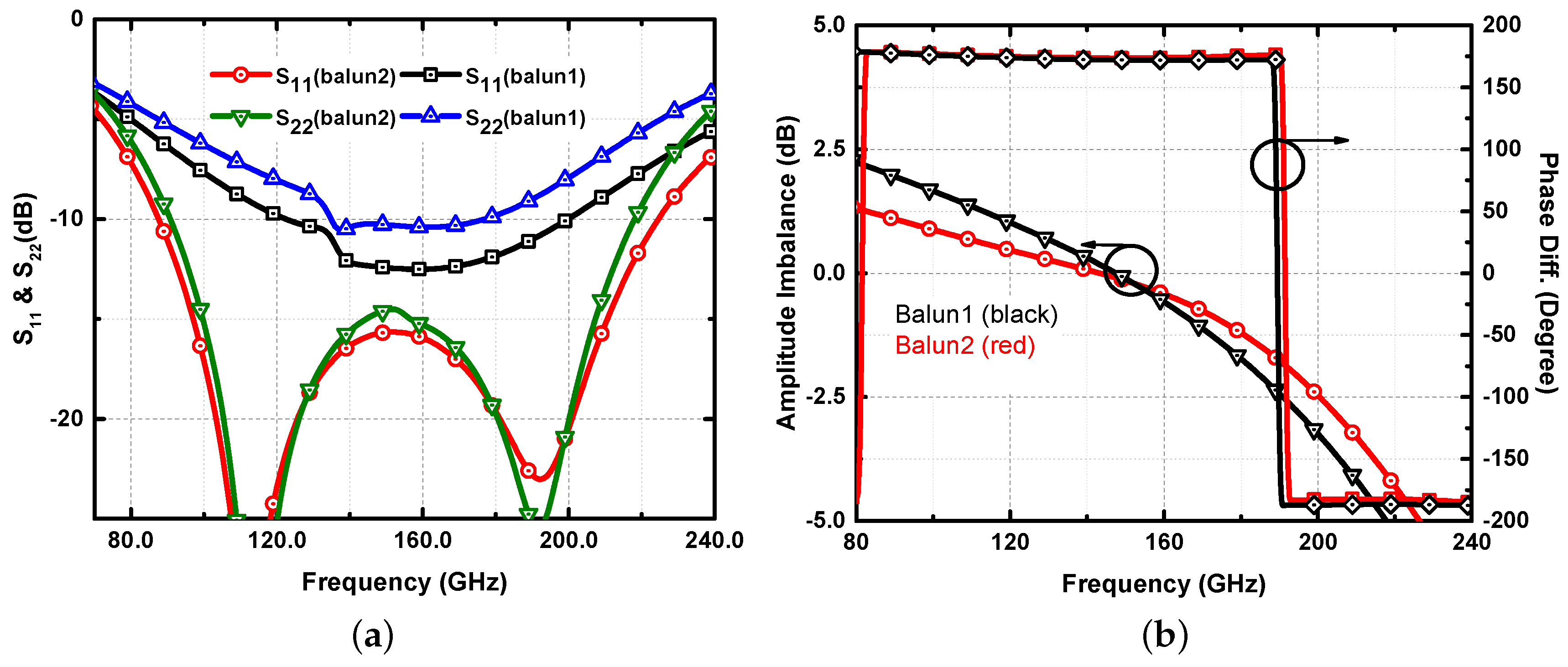
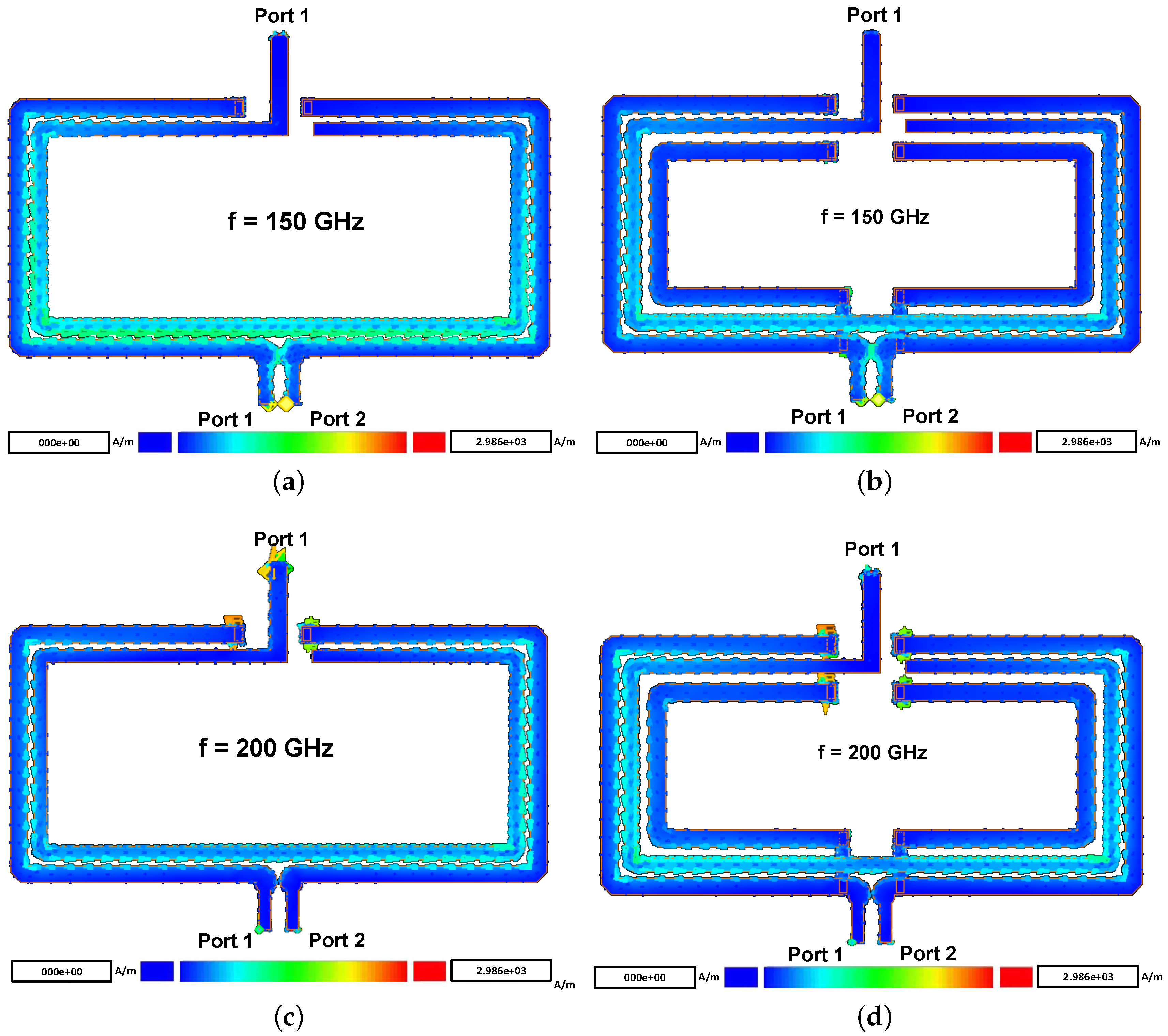
To see the advantages of three asymmetric coupled lines over the conventional two coupled lines in the balun design, the two baluns were EM-simulated in ADS momentum. The input and output reflection coefficients were found for the single-ended 50 and differential 100 loads, respectively. Figure 6 shows a comparison of the input and output reflection coefficients ( and ) (a) and the amplitude imbalance and phase difference (b) of the two baluns. In the case of Balun 1, and did not matched well to their respective port impedances over a wide bandwidth, which resulted in a large amplitude imbalance, as can be seen in Figure 6b. The main reasons for such performances were the weak coupling between the coupled lines and the lower even-odd mode impedance ratios, resulting in the even/odd mode phase velocity variation over the frequencies. In contrast, the asymmetric coupled line balun not only improved the capacitive coupling, it also adjusted the even/odd mode capacitances over a wider bandwidth, which enhanced the input and output matching and reduced the amplitude imbalance in the frequency band of 88–224 GHz. The phase difference was very close to ±180 in both cases. The surface current distribution of the two baluns is shown in Figure 7 at 150 and 200 GHz. At these two frequencies, the magnitude of the surface current was varying significantly for Balun 1, while it was almost similar for Balun 2. The surface current verified the performance of the proposed asymmetric three coupled line balun over the conventional two coupled line balun. Thus, the asymmetric coupled line balun improved the odd mode capacitances, which equalized the even/odd mode phase velocities needed for a high performance balun.
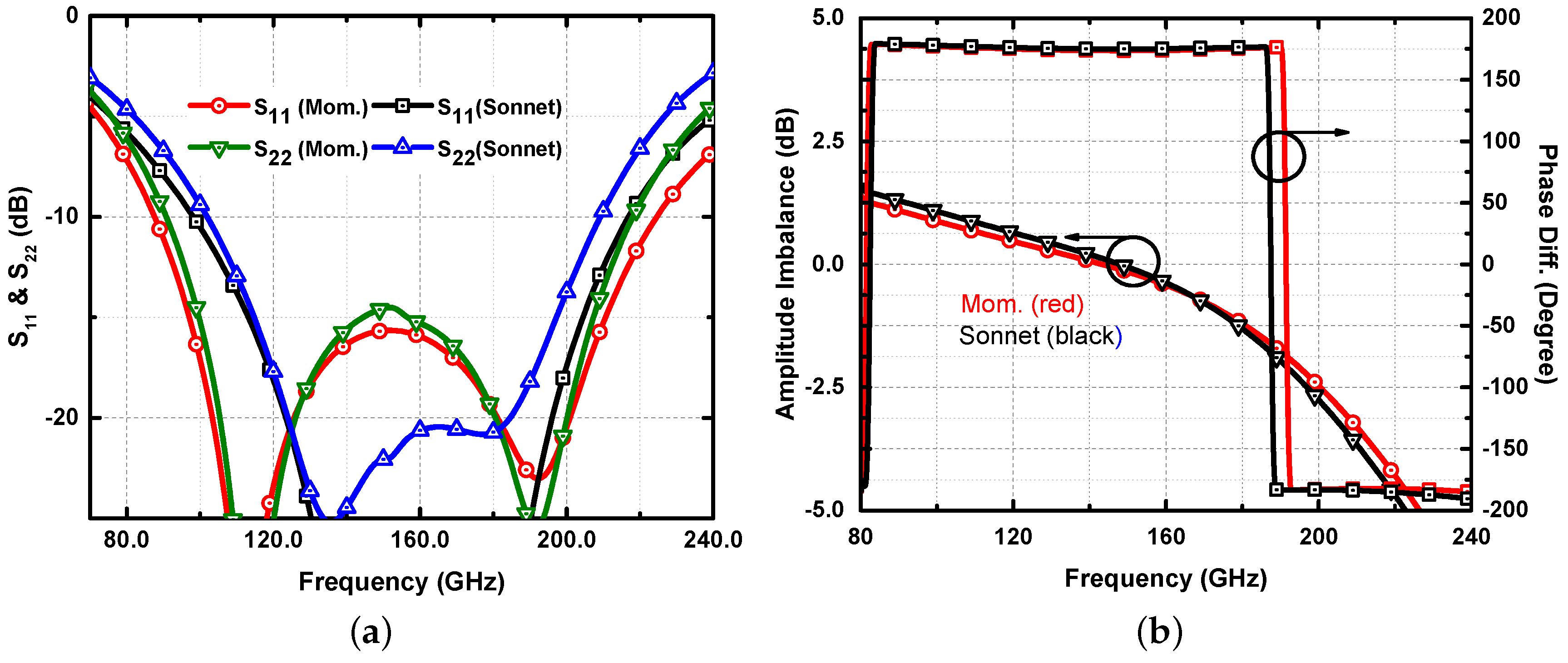
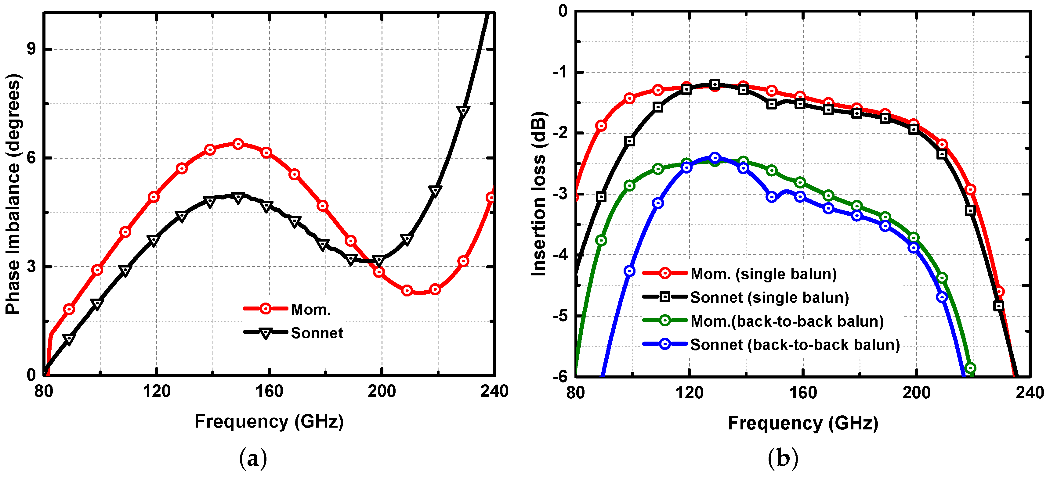
To validate the design of the asymmetric coupled line balun, it was also simulated in Sonnet EM-simulator. Figure 8 shows a comparison of and (a) and the amplitude imbalance and phase difference (b) of the balun in the two software programs. A good correlation was found between the two simulators. , were below −10 dB for the frequency band of 88–224 GHz, which covers the entire WR-6 (110–170 GHz) and WR-5 (140–220 GHz) frequency bands. The −10 dB reflection coefficient (S) bandwidth of the balun was 136 GHz. An amplitude imbalance of ±1 dB with a phase difference close to ±180 was found in the frequency range of 94–177 GHz.
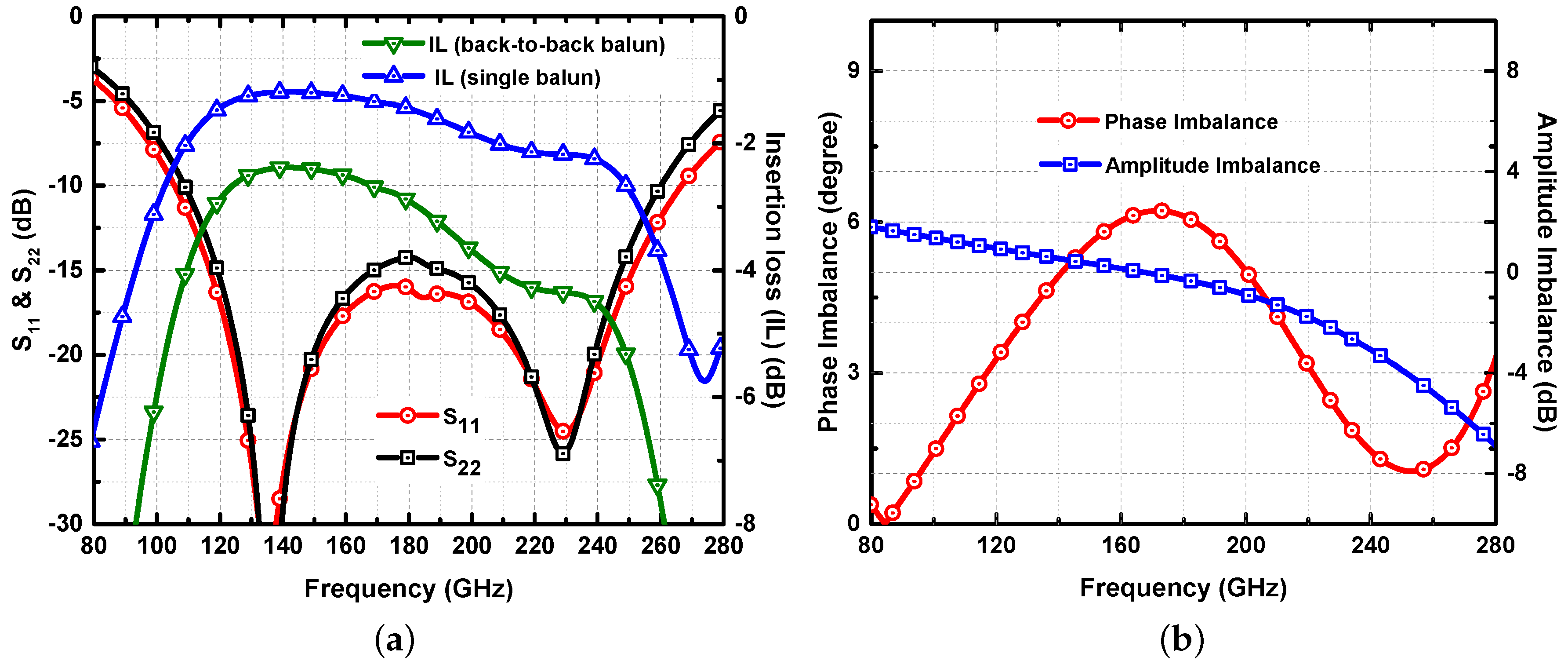
Figure 9 shows the phase imbalance (a) and insertion loss (b) of the balun. The phase imbalance was less than seven degrees. The minimum and maximum insertion losses of two back-to-back baluns including RF-pads in the D-band were 2.45 and 3 dB, respectively, which exhibited less than 1.5 dB of maximum insertion loss for the single balun. Above 200 GHz, the performances of the balun were degraded due to mismatches. A simple re-scaling of the size of balun can improve its performance. For this reason, the balun’s earlier dimensions of 215 × 148 m were modified to 175 × 148 m, and the resulting input/output reflection coefficients, insertion loss and phase and amplitude imbalances are shown in Figure 10. As can be seen, , and were improved over a wider frequency range of 106–266 GHz (WR-6, WR-5, and WR-4), which made the impedance bandwidth ( and <−10 dB) close to 160 GHz. The maximum losses of the single balun including RF-pad in WR-5 and WR-4 were 2.1 dB and 3.8 dB, respectively. The phase imbalance was less than seven degrees across all frequencies. Furthermore, the amplitude imbalance was <1 dB at most of the frequencies. However, there were some limitations arising from the frequency-dependent conductor losses and asymmetry of the balun itself. These limitations resulted in higher amplitude imbalances, which were more visible at the higher frequencies.
Table 1 shows a summary of the various state-of-the-art baluns at different frequencies. It can be clearly seen that both baluns reported in this paper outperformed, in terms of the critical parameter, the existing baluns based on similar technologies. Most of the earlier baluns either presented higher losses or limited bandwidth. Such performances of the balun are state-of-the-art, which makes it highly suitable for the future broadband differential circuits for various applications including imaging, spectroscopy, radar, and high-speed data communication. Furthermore, the balun reported in this paper can be easily re-scaled to cover other frequencies of interest. However, due to the frequency-dependent conductor losses and asymmetry of the balun, the re-scaling can cause slightly higher amplitude imbalances at some frequencies.
4. Conclusions
Two high performance baluns based on three asymmetric coupled lines have been presented. The asymmetric coupled lines improved the odd mode capacitances, which increased the even/odd mode impedance ratio over a wider bandwidth. Thus, lower values for the insertion loss and phase and amplitude imbalance can be achieved over a wider bandwidth. The baluns have been developed with the standard 130-nm SiGe BiCMOS BEOL process to cover the WR-6, WR-5, and WR-4 frequency bands. State-of-the-art performances have been achieved in terms insertion loss, reflection coefficients and phase and amplitude imbalances. In the future, the baluns can be utilized to design, test, or characterize broadband differential circuits at sub-THz frequencies for various applications including radar, imaging, spectroscopy, and high-speed data communication. Furthermore, the amplitude imbalances coming from the conductor losses and asymmetry of the balun at higher frequencies can be addressed in the future.
Author Contributions
Conceptualization, A.A.; Formal analysis, A.A.; Investigation, A.A.; Methodology, A.A.; Resources, D.K., P.C.; Software, D.K., P.C.; Supervision, P.C.; Writing—original draft, A.A.; Writing—review and editing, A.A., J.Y., H.J.N., D.K., F.G., and P.C.; For other cases, all authors have contributed equally.
Funding
This research was funded by H2020 ITN CELTA grant number 675683.
Acknowledgments
The authors would like to thank the H2020 ITNCELTAunder Grant Number 675683 of Call: H2020-MSCA-ITN-2015.
Conflicts of Interest
The authors declare no conflict of interest.
References
- Heinemann, B.; Barth, R.; Bolze, D.; Drews, J.; Fischer, G.G.; Fox, A.; Fursenko, O.; Grabolla, T.; Haak, U.; Knoll, D.; et al. SiGe HBT technology with fT/fmax of 300GHz/500GHz and 2.0 ps CML gate delay. In Proceedings of the 2010 International Electron Devices Meeting, San Francisco, CA, USA, 6–8 December 2010; pp. 30–35. [Google Scholar] [CrossRef]
- Kucharski, M.; Kissinger, D.; Ng, H.J. Scalable 79- and 158-GHz integrated radar transceivers in SiGe BiCMOS technology. In Proceedings of the 2018 22nd International Microwave and Radar Conference (MIKON), Poznan, Poland, 14–17 May 2018; pp. 342–344. [Google Scholar] [CrossRef]
- Wang, D.; Schmalz, K.; Eissa, M.H.; Borngräber, J.; Kucharski, M.; Elkhouly, M.; Ko, M.; Ng, H.J.; Kissinger, D. Integrated 240-GHz Dielectric Sensor With dc Readout Circuit in a 130-nm SiGe BiCMOS Technology. IEEE Trans. Microw. Theory Tech. 2018, 66, 4232–4241. [Google Scholar] [CrossRef]
- Laemmle, B.; Schmalz, K.; Scheytt, J.C.; Weigel, R.; Kissinger, D. A 125 GHz Permittivity Sensor With Read-Out Circuit in a 250-nm SiGe BiCMOS Technology. IEEE Trans. Microw. Theory Tech. 2013, 61, 2185–2194. [Google Scholar] [CrossRef]
- Sarkas, I.; Hasch, J.; Balteanu, A.; Voinigescu, S.P. A Fundamental Frequency 120-GHz SiGe BiCMOS Distance Sensor With Integrated Antenna. IEEE Trans. Microw. Theory Tech. 2012, 60, 795–812. [Google Scholar] [CrossRef]
- Dacquay, E.; Tomkins, A.; Yau, K.H.K.; Laskin, E.; Chevalier, P.; Chantre, A.; Sautreuil, B.; Voinigescu, S.P. D-Band Total Power Radiometer Performance Optimization in an SiGe HBT Technology. IEEE Trans. Microw. Theory Tech. 2012, 60, 813–826. [Google Scholar] [CrossRef]
- Zhao, Y.; Ojefors, E.; Aufinger, K.; Meister, T.F.; Pfeiffer, U.R. A 160-GHz Subharmonic Transmitter and Receiver Chipset in an SiGe HBT Technology. IEEE Trans. Microw. Theory Tech. 2012, 60, 3286–3299. [Google Scholar] [CrossRef]
- Eissa, M.H.; Malignaggi, A.; Wang, R.; Elkhouly, M.; Schmalz, K.; Ulusoy, A.C.; Kissinger, D. Wideband 240-GHz Transmitter and Receiver in BiCMOS Technology With 25-Gbit/s Data Rate. IEEE J. Solid-State Circuits 2018, 53, 2532–2542. [Google Scholar] [CrossRef]
- Kissinger, D.; Rothbart, N.; Schmalz, K.; Bornzraber, J.; Hx00FCbers, H.W. Sensitive Millimeter-Wave/ Terahertz Gas Spectroscopy Based on SiGe BiCMOS Technology. In Proceedings of the 2018 43rd International Conference on Infrared, Millimeter, and Terahertz Waves (IRMMW-THz), Nagoya, Japan, 9–14 September 2018; pp. 1–2. [Google Scholar]
- Ang, K.S.; Robertson, I.D. Analysis and design of impedance-transforming planar Marchand baluns. IEEE Trans. Microw. Theory Tech. 2001, 49, 402–406. [Google Scholar] [CrossRef]
- Ang, K.S.; Leong, Y.C.; Lee, C.H. Analysis and design of miniaturized lumped-distributed impedance-transforming baluns. IEEE Trans. Microw. Theory Tech. 2003, 51, 1009–1017. [Google Scholar] [CrossRef]
- Howard, D.C.; Cho, C.S.; Cressler, J.D. A broadband, millimeter wave, asymmetrical Marchand balun in 180 nm SiGe BiCMOS technology. In Proceedings of the 2012 IEEE Radio Frequency Integrated Circuits Symposium, Montreal, QC, Canada, 17–19 June 2012; pp. 425–428. [Google Scholar] [CrossRef]
- Zheng, S.; Pan, Y. A new Marchand balun with harmonic suppression. In Proceedings of the 2014 XXXIth URSI General Assembly and Scientific Symposium (URSI GASS), Beijing, China, 16–23 August 2014; pp. 1–4. [Google Scholar] [CrossRef]
- Johansen, T.; Krozer, V. Analysis and design of lumped element Marchand baluns. In Proceedings of the MIKON 2008—17th International Conference on Microwaves, Radar and Wireless Communications, Wroclaw, Poland, 19–21 May 2008; pp. 1–4. [Google Scholar]
- Chiou, H.; Yang, T. Low-Loss and Broadband Asymmetric Broadside-Coupled Balun for Mixer Design in 0.18-μm CMOS Technology. IEEE Trans. Microw. Theory Tech. 2008, 56, 835–848. [Google Scholar] [CrossRef]
- Xu, L.; Sjöland, H.; Törmänen, M.; Tired, T.; Pan, T.; Bai, X. A Miniaturized Marchand Balun in CMOS With Improved Balance for Millimeter-Wave Applications. IEEE Microw. Wirel. Compon. Lett. 2014, 24, 53–55. [Google Scholar] [CrossRef]
- Yen, H.; Huang, G.; Shiao, Y.J.; Huang, F. A compact millimeter-wave broadband stacked coupled balun. In Proceedings of the 2012 Asia Pacific Microwave Conference Proceedings, Kaohsiung, Taiwan, 4–7 December 2012; pp. 992–994. [Google Scholar] [CrossRef]
- Chiou, H.; Lin, J. Symmetric Offset Stack Balun in Standard 0.13-μmCMOS Technology for Three Broadband and Low-Loss Balanced Passive Mixer Designs. IEEE Trans. Microw. Theory Tech. 2011, 59, 1529–1538. [Google Scholar] [CrossRef]
- Song, I.; Schmid, R.L.; Howard, D.C.; Cressler, J.D. A 34-110 GHz wideband, asymmetric, broadside-coupled Marchand balun in 180 nm SiGe BiCMOS technology. In Proceedings of the 2014 IEEE MTT-S International Microwave Symposium (IMS2014), Tampa, FL, USA, 1–6 June 2014; pp. 1–4. [Google Scholar] [CrossRef]
- Ahmed, F.; Furqan, M.; Stelzer, A. A 200-325-GHz wideband, low-loss modified Marchand balun in SiGe BiCMOS technology. In Proceedings of the 2015 European Microwave Conference (EuMC), Paris, France, 7–10 September 2015; pp. 40–43. [Google Scholar] [CrossRef]
- La Spada, L. Metasurfaces for Advanced Sensing and Diagnostics. Sensors 2019, 19, 355. [Google Scholar] [CrossRef] [PubMed]
- Mohammadi Estakhri, N.; Edwards, B.; Engheta, N. Inverse-designed metastructures that solve equations. Science 2019, 363, 1333–1338. [Google Scholar] [CrossRef] [PubMed]
- La Spada, L.; Spooner, C.; Haq, S.; Hao, Y. Curvilinear MetaSurfaces for Surface Wave Manipulation. Sci. Rep. 2019, 9, 3107. [Google Scholar] [CrossRef] [PubMed]
- Vakil, A.; Engheta, N. Transformation Optics Using Graphene. Science 2011, 332, 1291–1294. [Google Scholar] [CrossRef] [PubMed]
- Spada, L.L.; Vegni, L. Near-zero-index wires. Opt. Express 2017, 25, 23699–23708. [Google Scholar] [CrossRef] [PubMed]
- Greybush, N.J.; Pacheco-Peña, V.; Engheta, N.; Murray, C.B.; Kagan, C.R. Plasmonic Optical and Chiroptical Response of Self-Assembled Au Nanorod Equilateral Trimers. ACS Nano 2019, 13, 1617–1624. [Google Scholar] [CrossRef] [PubMed]
- Mongia, R.; Bahl, I.; Bhartia, P. RF and Microwave Coupled-Line Circuits; Artech House: Norwood, MA, USA, 1998; pp. 109–114. [Google Scholar]
- Zhang, Z.Y.; Guo, Y.X.; Ong, L.C.; Chia, M.Y.W. A new planar marchand balun. In Proceedings of the IEEE MTT-S International Microwave Symposium Digest, Long Beach, CA, USA, 17 June 2005; pp. 1207–1210. [Google Scholar] [CrossRef]
- Ali, A.; Cipriani, E.; Johansen, T.K.; Colantonio, P. Study of 130 nm SiGe HBT Periphery in the Design of 160 GHz Power Amplifier. In Proceedings of the 2018 First International Workshop on Mobile Terahertz Systems (IWMTS), Duisburg, Germany, 2–4 July 2018; pp. 1–5. [Google Scholar] [CrossRef]
- Ali, A.; Cipriani, E.; Colantonio, P. Common emitter and cascode topologies at G band: A comparative study on a single stage 183 GHz power amplifier. In Proceedings of the 2018 International Conference on IC Design Technology (ICICDT), Otranto, Italy, 4–6 June 2018; pp. 81–84. [Google Scholar] [CrossRef]
Figure 1.
Symmetric coupled line with ports’ definition (a) and the conventional Marchand balun (b).
Figure 1.
Symmetric coupled line with ports’ definition (a) and the conventional Marchand balun (b).

Figure 2.
Capacitances of coupled lines under odd mode excitation (a) and even mode excitation (b).

Figure 3.
The 130-nm SiGe BEOLprocess cross-section [29].
Figure 3.
The 130-nm SiGe BEOLprocess cross-section [29].

Figure 4.
3D views of the conventional edged couple balun (a) and a three asymmetric coupled lines balun (b), where different important parameters are shown. For the sake of simplicity, the ground plane is not shown. The size of each balun is 215 × 148 m. Balun 1: conventional coupled line balun without the inner lines; Balun 2: the three asymmetric coupled lines balun. W, width; S, separation.

Figure 5.
Simulated input reflection coefficient (), amplitude imbalance, and phase difference for the two gap (S1 and S2) variations with fixed widths of W1 = 5 m and W2 = 6.5 m. under S1 (a) and S2 (b) variation, amplitude imbalance under S1 (c) and S2 (d) variation, insertion loss of a single balun under S1 (e) and S2 (f) variation, and phase difference under S1 (g) and S2 (h) variation. All parameters are in m, while absolute values of the phase difference are shown to clearly see the phase imbalance.

Figure 6.
Simulated input/output reflection coefficients (, ) (a) and amplitude imbalance and phase difference (b) of the two baluns.
Figure 6.
Simulated input/output reflection coefficients (, ) (a) and amplitude imbalance and phase difference (b) of the two baluns.

Figure 7.
Simulated surface current distribution at 150 GHz of Balun 1 (a) and Balun 2 (b) and at 200 GHz of Balun 1 (c) and Balun 2 (d).
Figure 7.
Simulated surface current distribution at 150 GHz of Balun 1 (a) and Balun 2 (b) and at 200 GHz of Balun 1 (c) and Balun 2 (d).

Figure 8.
Simulated , (a) and amplitude imbalance and phase difference (b) of the asymmetric coupled line balun in Sonnet and ADS momentum.
Figure 8.
Simulated , (a) and amplitude imbalance and phase difference (b) of the asymmetric coupled line balun in Sonnet and ADS momentum.

Figure 9.
Simulated insertion loss (a) and phase imbalance (b) of the asymmetric coupled line balun in Sonnet and ADS momentum.
Figure 9.
Simulated insertion loss (a) and phase imbalance (b) of the asymmetric coupled line balun in Sonnet and ADS momentum.

Figure 10.
Simulated S, S insertion loss (a) and amplitude and phase imbalance (b) of the re-scaled asymmetric coupled line balun.
Figure 10.
Simulated S, S insertion loss (a) and amplitude and phase imbalance (b) of the re-scaled asymmetric coupled line balun.


Table 1.
State-of-the-art balun comparison.
| f (GHz) | Technology | Topology | Insertion Loss (min.–max.) (dB) | Amplitude Imbalance (dB) | Phase Imbalance (degree) | Ref. |
|---|---|---|---|---|---|---|
| 16.5–67 | 180-nm CMOS | Asymm.stack | (1.1–4) | 1 | 5 | [15] |
| 57–67 | 65-nm CMOS | With groundedT-bars | (1.5–3.5) | 0.5 | 1 | [16] |
| 27.6–65.5 | 65-nm CMOS | Stack | (2.8–4.2) | 0.8 | 8 | [17] |
| 20–67 | 130-nm CMOS | Symm.offset stack | (1.4–3) | 1 | 4 | [18] |
| 34–110 | 180-nm SiGe BiCMOS | Stack | (1.7–4.7) | 1.5 | 7 | [19] |
| 200–325 | 130-nm SiGe BiCMOS | 3-line symm. edge coupled | (2.5–3.3) | 1.5 | 10 | [20] |
| 88–224 | 130-nm SiGe BiCMOS | 3-line asymm. edge coupled | (1.2–1.5) (1.2–3) | <1 | <7 | This Work |
| 106–262 | 130-nm SiGe BiCMOS | 3-line asymm. edge coupled | (1.2–1.9) (1.2–2.1) (1.35–3.8) | <1 <1.8 | <6.2 | This Work |
Results using EM simulation of the baluns in ADS momentum. The 3-dB loss due to splitting is not included. Valid in the frequency band of 200–273 GHz. Valid for the WR-6 band (110–170 GHz). Valid for the WR-5 band (140–220 GHz). Valid for the WR-4 band (170–260 GHz).
© 2019 by the authors. Licensee MDPI, Basel, Switzerland. This article is an open access article distributed under the terms and conditions of the Creative Commons Attribution (CC BY) license (http://creativecommons.org/licenses/by/4.0/).
Share and Cite
MDPI and ACS Style
Ali, A.; Yun, J.; Jalli Ng, H.; Kissinger, D.; Giannini, F.; Colantonio, P. High Performance Asymmetric Coupled Line Balun at Sub-THz Frequency. Appl. Sci. 2019, 9, 1907. https://doi.org/10.3390/app9091907
AMA Style
Ali A, Yun J, Jalli Ng H, Kissinger D, Giannini F, Colantonio P. High Performance Asymmetric Coupled Line Balun at Sub-THz Frequency. Applied Sciences. 2019; 9(9):1907. https://doi.org/10.3390/app9091907
Chicago/Turabian StyleAli, Abdul, Jongwon Yun, Herman Jalli Ng, Dietmar Kissinger, Franco Giannini, and Paolo Colantonio. 2019. "High Performance Asymmetric Coupled Line Balun at Sub-THz Frequency" Applied Sciences 9, no. 9: 1907. https://doi.org/10.3390/app9091907
Note that from the first issue of 2016, this journal uses article numbers instead of page numbers. See further details here.