Perovskite Thin Film Materials Stabilized and Enhanced by Zinc(II) Doping


1
Molecular Photonics Group, Van ’t Hoff Institute for Molecular Sciences (HIMS), Universiteit van Amsterdam, Postbusnummer 94157, 1090 GD Amsterdam, The Netherlands
2
Center for Nanophotonics, Institute AMOLF, Science Park 104, 1098 XG Amsterdam, The Netherlands
*
Author to whom correspondence should be addressed.
Appl. Sci. 2019, 9(8), 1678; https://doi.org/10.3390/app9081678
Submission received: 2 April 2019
/
Revised: 16 April 2019
/
Accepted: 17 April 2019
/
Published: 23 April 2019
(This article belongs to the Special Issue Materials and Optical Strategies for Solar Cells: Recent Advances and Challenges)
Abstract
:Featured Application
Doping lead perovskite materials with a few percent of zinc-halides increases their stability at ambient conditions, enhances their properties and improves the efficiency of the corresponding solar cell devices.
Abstract
Recent work of ten different groups shows that the application of zinc-halides in lead perovskite materials results in a contraction of the d-space, stronger interaction with the organic cation, improved crystallization with larger crystal domains, a Goldschmidt factor closer to unity, smoother and denser thin films and an even distribution of Zn(II) (at the Pb(II) sites) throughout the material. These combined effects may lead to: (1) a substantially higher stability (even at ambient or high humidity conditions); (2) enhanced luminescent properties; (3) a higher power conversion efficiency (PCE) of the corresponding solar cell devices (up to PCE ~20%, with enhancement factors of 1.07 to 1.33 relative to undoped material).
1. Introduction: Perovskite Solar Cells on the Rise
The search for novel photovoltaic materials has intensified over the past few decades as the demand for cleaner energy sources grows. A huge surge in research focusing on third generation photovoltaic devices has brought forth dramatic improvements in device performances as power conversion efficiencies start approaching the Shockley–Queisser limit [1]. In particular, perovskites have received a tremendous amount of attention, since these materials provide a cheap route to highly efficient photovoltaic materials. The rapid increase in performance of lead-based metal-halide perovskite solar cells over the past years has resulted in solar cells with efficiencies of 24.2% [2]. In conjunction with reports that perovskite devices are stable over longer periods of time [3,4] this demonstrates that it is not unimaginable that perovskites will be suitable for commercialization in the foreseeable future. In this quest it is imperative to compositionally tailor the devices by engineering the ionic composition of the ABX3 lattice [5]. The bandgap of a device can be tuned by using mixed halides [6]. Similarly, the thermal stability and photo-stability of lead-based perovskites can be improved by (partially) replacing the conventional organic cation, methylammonium (MA), by formamidinium (FA) [5]. Despite the extensive research efforts focusing on these perovskites, there have been surprisingly few reports discussing the effects of the partial substitution of the Pb2+ ions at the B-site of the perovskite crystal lattice. It remains elusive how partial substitution of the lead ions in the B-site with a particular alternative metal species influences the material properties and photovoltaic performance. It has been demonstrated that the introduction of certain hetero-valent metals in perovskite films influences both the optoelectronic and crystallographic properties of the resulting film. The introduction of In3+ increases crystallinity and morphology of the film [7]. Through the homo-valent substitution of Pb2+ with Sn2+ the first example successfully replacing lead on the B-site of the crystal lattice (with tin) was observed, resulting in a narrower bandgap [8]. However, a big drawback is the ability of Sn2+ to oxidize to Sn4+ in situ making Sn less suitable as doping material. In 2017, a whole new set of homo-valent metals were explored as dopants in perovskite lattices. It was soon discovered that lead could partially be replaced by Co2+, Zn2+, Mg2+, Mn2+, Ni2+ due to their similar atomic radii and divalent nature [9], also in perovskite nanocrystals [10]. Not long after this, several extensive studies focused on doping with Zn2+ commenced [11,12,13,14,15,16]. Zinc is particularly interesting due to its non-toxic nature, its inability to oxidize or reduce easily, and its abundance on Earth. The result of doping with several percentages of Zn(II) were smoother and denser films with fewer pinholes. Zn2+ features a stronger interaction towards the MA+ cation and I− anion. The smaller ionic radius of Zn(II) compared to Pb(II) causes a unit cell contraction of the hh0-plane and this results in enhanced nucleation and crystallization during fabrication, resulting in bigger grains and fewer pinholes. This is beneficial for efficiency because non-radiative losses are generally attributed to Grain Boundaries (GBs), so by reducing the number of GBs (due to the enlargement of perovskite domains) losses are also reduced. However, this also induces increased stabilization of the resulting film towards degradation, which commences at grain boundaries and at pinholes.
In this review, we compile recent results on the use of zinc–iodide and zinc–chloride for doping or alloying of perovskite materials for solar cells. We highlight important results and give an overview of unifying comprehension obtained in the last two years regarding the aspects that play a role in the effects of Zn(II) in perovskites. This review focusses on papers reporting about Zn(II) in perovskites published between 8 December 2016 and 5 December 2018. For more background information on perovskites and their solar cells we refer to several extensive recent reviews on this general topic [17,18,19].
2. Doping of Perovskites with Mono- and Tri-Valent Metals
Doping of perovskites with hetero-valent cations is an intriguing subject and there is little consensus on the exact mechanism behind improved properties of hetero-valent doped perovskites. Abdi-Jalebi et al. [20] reported the doping of MAPbI3 with monovalent halide-based salts such as NaI, CuBr, CuI and AgI. The formed structures were studied with scanning electron microscopy (SEM) and the resulting structures are depicted in Figure 1.
On the left, PbI2 is depicted and on the right the pristine MAPbI3 and after doping with CuBr, CuI, NaI and AgI, respectively. Undoped MAPbI3 appears in large tetragonal shaped perovskite crystals on top of the TiO2 but when the material is doped with CuBr, the TiO2 is relatively better covered (Figure 1b). Moreover, the TiO2 layer is considerably better covered with continuous and uniform perovskite when the material is doped with CuI and AgI (Figure 1c,e). The perovskite films including CuI and AgI additives are reported to be nearly pinhole free as compared to pristine and other samples. Additionally, it was concluded that such doping has had significant effects on the absorption and hole motilities when compared to pristine MAPbI3. The exact roles of these proposed “dopants” are still not entirely clear.
Reports with inconsistent conclusions are published on doping of perovskite structures with Bi3+. Snaith et al. reported [21] on the introduction of Bi3+ in MAPbBr3. They referred to earlier reports [7] by Abdelhady and co-workers. Abdelhady et al. claimed that hetero-valent doping of MAPbBr3 with Bi3+ caused a four orders of magnitude conductivity enhancement and a significant bandgap narrowing within the resulting material. Snaith, on the other hand, reported that no metal-halide octahedral lattice tilting was observed. The angle between X-B-X in two unit cells in a lattice is directly correlated with the bandgap of the overall material. The bandgap-change due to Bi3+ doping was a result of misinterpretation from light transmission measurements that were caused by a color change that arose due to the introduction of crystal defects. Snaith additionally reported that Bi3+ introduction is detrimental to device performance at all concentrations. Crystal defects are introduced upon doping and unfavorable non-radiative recombination is facilitated as a consequence.
A report [22] from 2016 by Snaith et al. described the doping of perovskite with Al3+. The ionic radius of Al3+ is much lower than Pb2+ (53 vs 119 pm) and it was therefore not expected that Al would replace Pb in the lattice. Extensive analysis with crystallography and mass spectroscopy revealed that Al3+ was not significantly incorporated in the lattice but expelled to the surface and grain boundary edges during the crystallization process. All evidence considered, Snaith et al. conclude that a small amount of Al3+ doping results in better crystallization with fewer crystal defects in the film.
The exact mechanism behind this is difficult to determine; however, they postulate a mechanism as follows: impurity ions can slow down crystallization by absorbing to the surface of the crystal and sterically inhibiting growth. Another mechanism could be that these impurities alter the surface energy of the crystal growth front, accelerating crystallization. In low concentrations, they infer that Al3+ facilitates enhanced crystallization and especially the growth of the (hh0)-plane, resulting in better orientated crystalline domains. In Figure 2, a schematic diagram of the perovskite grown under the influence of the Al3+ doping is depicted. In the left column of Figure 2, it is illustrated how crystal defects, which potentially exist in the form of terraces, grow under normal conditions. On the right it is indicated how Al3+ doping selectively enhances growth of these sites, aiding the formation of a smoother perovskite surface with less defects.
These examples (Na1+, Cu1+, Ag1+, Bi3+, Al3+) show that the presence of mono- or tri-valent metal ions strongly influences the crystallization properties of perovskite films. No clear general behavior can be inferred, predicting which metal ions improve properties.
3. Doping of Perovskites with Zinc(II)
Following up on the Belcher report [9] (2016), much more effort was put into research on the partial replacement of lead with zinc. Belcher et al. reported that the perovskite lattice is tolerant to non-VI group elements, such as: Co2+, Cu2+, Sn2+ and Zn2+ (from zinc–acetate). Among these elements, Zn stands out due to certain characteristics that make it particularly interesting. At first, Zn is abundantly available in the Earth’s crust, non-toxic and therefore a welcome partial replacement for lead. Zn(II) is a medium-sized transition metal and its atomic radius (74 pm) is considerably smaller than the one of lead(II) (119 pm [22]). Furthermore, zinc has a suitable valence state and is reported to be resistant against reduction and oxidation processes [16]. The theoretical Goldsmith tolerance factor (t) for a generic ABX3 perovskite is calculated as shown in Equation (1).
Here, rA, rB, and rX are the (average) ionic radii for the cation (A), metal (B), and halide (X) sites, respectively. If the tolerance factor is in the range 0.813–1.107, perovskites can form. The Goldsmith factor expresses how close the geometry is to an ideal undistorted perovskite packing, with a perfect cubic base as the ideal 1. For MAPbI3 and FAPbI3 these reported factors range between 0.92–0.95 and 1.03–1.04, respectively. The tolerance factor of CH3NH3ZnI3 is calculated to be 1.05. In this calculation the atomic radii for methyl ammonium (RA) and iodine (RX) are 0.18 nm and RX = 0.22 nm, respectively [12]. Due to the tolerance factor of CH3NH3ZnI3 being very close to 1, it is expected that Zn2+ has the ability to form CH3NH3Pb1−xZnIxI3−yCly and this can be considered a first step in the assumption that Zn2+ (in contrast to Al3+) actually incorporates in the perovskite lattice and that Zn can have profound effects on the electronic and structural properties of the resulting material [13]. Values of t between 0.94 and 0.98 have been correlated with optimal device efficiencies. The Goldsmith tolerance factor (t) is a simple first limited approach to correlate structure to function. Crystal size, grain boundaries effects and dark quenching states however, are of more practical importance for device performance of perovskite materials. It is important to note that for some ions various radii are available depending on coordination.
Muscarella et al. reported [16] FA/MA-based lead perovskite materials with enhanced stabilization due to doping with 2.5% ZnI2 and the addition of 3-chloropropyl ammonium chloride (CPACl). The material, FA0.85MA0.15Pb0.975Zn0.025I2.85Br0.15-[CPACl] was spin-coated and annealed and resulted in a compact dense homogenous pinhole-free layer. (Additives are denoted in square brackets in this review). During the annealing step CPACl was gradually evaporated from the structure gradually changing the FA/MA: CPACl ratio. During this gradual change, the lattice organization is induced and leads to the stacking of preformed crystalline units yielding an organized and protected final product. Goldsmith tolerance factor for the perovskite containing 2.5wt% Zn(II) is 0.981 compared to 0.978 for the full Pb-perovskite. The process is schematically depicted in Figure 3. They used X-ray diffraction (XRD) to confirm that that Zn2+ is incorporated in the lattice on a Pb2+ position. This composition can also be used in a solvent free grinding method, giving easy access to perovskite pellets. The final product featured protective alkyl tails that stabilized the structure. The photoluminescence of the thin film material was studied with confocal microscopy, directly deposited on indium tin oxide (ITO), leading to charge injection (see Figure 4). The confocal microscopy indicates a dense network of similarly shaped hexagonal and pentagonal perovskite microcrystals, with ~500 nm dimensions. The ratio (lifetime/intensity) accentuates the special character of the grain boundaries, that show properties different from the bulk (or the centers of the crystals). These materials remain black without substantial loss of sharp XRD features even after 1440 h at ambient (Dutch) indoor conditions.
In 2017, Zhao et al. reported [15] the partial replacement of Pb2+ by Zn2+ in MAPbI3 perovskites. The emphasis was on the effects of zinc doping (with ZnI2) on morphology, optical, electronic and photovoltaic performance. The zinc substituted perovskite layers, here denoted as MA(Pb:Zn)I3, were prepared through solution processing. It appears that no chloride components were used. Soon it was clear that the addition of small quantities of Zn strongly enhances the charge carrier collection efficiency of the cell leading to a higher overall efficiency. It was witnessed that the carrier lifetime of the device increased linearly with the increasing Zn content up to 15%. Other important enhancements were the morphology and crystallinity of the film. The presence of Zn enlarges the grain size and reduces the grain boundary surface. Nonradiative recombination takes place at these grain boundary surface and as a consequence the presence of zinc reduces the non-radiative recombination having an advantageous effect on efficiency. Because morphology and coverage of the perovskite film is of such essence, Zhao et al. tried various preparation conditions to create a densely packed perovskite film with large grains and a highly covered surface. As shown in the first entries of Figure 5a–c, undoped perovskite features small grains and therefore a high grain boundary area. When the Zn concentration is raised the grain size increases, which suggest that Zn has a profound effect on the nucleation and subsequent crystal growth processes that occur during the fabrication processes. When the structure is doped with 15% Zn the material contains many pinholes that can cause low-resistant leakage pathways. The search for optimal Zn concentrations and annealing temperatures yielded a film with a 5% Zn content annealed for 10 min at 120 °C. Large grains are visible and no pinholes are present in this film.
By studying the XRD spectrum shown in Figure 6 it became clear that pure tetragonal perovskite was formed and that there were no impure phases, such as PbI2, present. When the spectrum was locally enlarged, the peak with the diffraction angle (θ) of 110 (see Figure 6b), a shift towards a higher degree was observed upon increase of Zn content. This is attributed to the Zn atoms with smaller atomic radii occupying larger Pb-sites. This finding is a second strong indication that Zn dopants are incorporated in the perovskite lattice.
Dai et al. came forward with a thorough work [14] on the doping of Pb perovskite with 3% of the transition metals Zn2+, Mn2+ and Ni2+. The resulting materials were mixed dimensional perovskite films (MA(Pb:M)I3) with a higher stability and in the case of the Zn2+ (from ZnI2), a superior photovoltaic performance of 18.35% (PCE, power conversion efficiency) (a 30% increase relative to undoped devices). Especially interesting was the moisture resistance and enhanced thermal resistance of the devices. The device operated for 800 h at 50% relative humidity and for 100 h at 60 °C. The results regarding blue shift, lattice contraction and XRD peak-shifts were similar to other papers discussed in this review. However, a deep reasoning behind the improved stability was provided by the authors. Three reasons were provided to unravel the mechanism behind the improved stability. At first, the doped perovskite features a much higher film quality with less internal defects. This suppresses degradation, which is taking place on those defect surfaces: the edges of pinholes. Secondly, the mixed dimensional perovskite now features a 2D layer that forms an insulating ’wall’ around the 3D material and consequently guards this system from decomposition. A third reason is that the tolerance factor of the doped mixed dimensional perovskite structures yields tolerance factors much closer to 1 than pristine perovskite, thus, displaying improved stability against humidity and heat. It appears that no chloride or bromide components were used in this work.
4. Influence of Zinc(II) on the Crystallization Mechanism
Han et al. published [13] a thorough reasoning on the positive effects that Zn content has on the properties of perovskite solar cells (MA(Pb:Zn)I3-[Cl-]). They hypothesized that Zn2+ forms a perovskite structure with MA+ and I−. Additionally, they report that Zn has a higher interaction with MA. This was confirmed by using attenuated total refraction Fourier Transform Infra-Red spectroscopy (ATF-FTIR) to study the stretching frequency of symmetrical NH3+ in a pristine sample of CH3NH3I and when incorporated in a perovskite structure. As shown, stretching vibration of symmetrical NH3+ in a CH3NH3I sample appears to be at 3086 cm−1 while the stretching vibration shifts to 3122 cm−1 in pure and doped perovskite due to its interaction with Pb or Zn. However, it is now obvious that the stretching intensity increases when CH3NH3I is in the direct presence of Zn. This indicates that there is a stronger interaction between CH3NH3I and Zn. From this it can be stated that Zn2+ increased the crystallinity of the hh0-plane of the unit cell in which the Pb is replaced by Zn. This contracts the distance between adjacent lattice planes (d-space), which could cause the formation of bigger grains.
A more exact mechanism is described as follows: the precursors that were used to prepare the device were PbCl2 and CH3NH3I. Zinc was introduced in the form of ZnCl2. After annealing the Cl- is released from the perovskite system by forming CH3NH3Cl gas and the resulting perovskite structure is CH3NH3Pb1-xZnxI3-yCly. Due to the replacement of a small quantity of Pb2+ by Zn2+, the crystallization process has been changed. As shown in Figure 7d, it was hypothesized that the stronger interaction of Zn2+ with the anions and the strong coordination with the organic group makes the perovskite system to grow into bigger grains. This is in line with the observation that the over-doped perovskite systems result in grains that are so big that areas with pinholes arise in between and the general coverage is affected. Note that we indicate additives in square brackets after the composition, e.g., [Cl−].
To fully confirm that Zn is indeed incorporated in the lattice X-ray diffraction measurements were carried out at different concentrations of Zn2+: upon increase of the Zn2+ content the peak representing the 110 plane is slightly shifted to a higher degree, which indicates that the d-space of cells contract when they are doped with Zn (as shown in Figure 6b, reported in Reference [15]). The contraction of the d-space can be explained the aforementioned higher chemical bond with MA+ and I and Zn’s smaller ionic radius [11,13,15]. Zinc chloride and lead chloride precursors were used in Reference [13].
A last conformation for the researchers that Zn was evenly dispersed over the lattice was obtained through elemental mapping using energy dispersive X-ray spectroscopy (EDS). The obtained image is displayed in Figure 8 and reveals that Zn2+ ions are uniformly distributed in the seeds of the perovskite film and not aggregated at the grain boundaries.
5. Optical Properties, Band Bending and Device Improvement
Next to improved stability and better device performance, a general observation upon doping with Zinc(II) is an enhanced emission intensity and a longer emission lifetime. Quantitative data of emission yield and lifetimes are easily influenced by various factors so that uniformity around data of different groups is not observed, but the general trend is that enhanced emission and longer lifetimes are reported for a certain doping level (relative to undoped materials), see Table 1. A representative example [11] is given in Figure 9. The optimum in optical properties observed here is clearly at ~3%, which is also reported by other groups.
It is important to note that for all thin films, Zn(II) incorporation enhances the photoluminescence lifetime for all doping levels. Furthermore, the lifetime of the composition reported by Muscarella et al. changes from 12 ns on ITO [16] to 1548 ns on quartz [24], indicating a quenching factor of 129 by ITO interaction (charge injection). This 1548 ns value is similar to the long emission lifetimes (2835 and 1105 ns) reported for recent record-breaking material compositions [25,26].
The addition of transition metals like Zn(II) can also be used to tailor the band bending [9]. These bands are important with regards to the barrier for charge injection into the charge transport layers of the solar cell devices. If we assume that the tailoring of the band bending for Zn(II) follows the same trend as for Co(II), an optimum between 1.6 and 6% of Zn(II) content [9] is anticipated. These results clearly set the stage for further optimization, where a clear distinction between MAPbI3 and FAPbI3-based materials has to be made. It also has to be noted that also the chemical source of Zn(II) can play a role, where zinc acetate, zinc chloride and zinc iodide not necessarily result in the exact same behavior.
Several groups have reported improved solar device performance upon Zn(II) incorporation. Power conversion efficiencies up to 20.06% [23] (with 1% of Zn(II) content) and enhancement factors of 1.07 to 1.33 (when comparing undoped and doped devices) are the trend. A PCE of 18.2% was reported by using 3% of ZnCl2 in 2017 [11] and 18.35% in 2018 [14] with 3% ZnI2. A similar value (PCE = 18.25%) was found for 5% Zn(II) [15]. The largest enhancement factor of 1.33 was obtained for 0.1% Zn(II), attaining a final PCE of 16.3% [13]. An overview of a selection of reported PCEs is given in Table 2. It is important to stress that the reported consecutive world record devices (e.g., see Reference [25] containing a phenethylammonium iodide additive (PEAI) and Reference [26] containing tri-iodide, (I3)− addition) do not contain Zn(II), but judging from the various reports reviewed here, it would certainly be interesting to look at the effect of Zn-doping on the PCE of record-breaking compositions.
Next to the clear effects of zinc doping, enhancing efficiency by a factor between 1.07 and 1.33, we also compile some record-breaking compositions in Table 2 (that do not contain zinc) as a historic overview. Since 2015, all record devices are based on FA/MA compositions. From Table 2, it can be seen that the compositional engineering that is accompanied by PCE increase is trending towards a higher FA content (compare References [5,27]) as well as a reduced Br content (compare References [25,26]). MA and Br however, seem to be essential for stability and phase-change behaviour. Iodide management [26] and alkyl-ammonium-based additives (see References [16,24,25]) are important factors to control defect states, which quench photoluminescence (see also Table 1). The presence of chloride (Cl−) in the precursor solution generally has a positive effect, but chloride is undetectable in the final thin films (see for example Reference [24]).
It has to be realized that these records are so-called “hero-devices”: in the statistical distribution of ~100 devices, they represent the high-end tailing of the gaussian distribution curve of the PCE. To reproduce these certified efficiencies of very small cells is highly challenging, even for research groups that specialize in perovskites. Exact experimental details and specific lab-based conditions and protocols that determine the perfect perovskite solar cell of a particular composition are not well understood. However, the whole field of perovskite solar cells is loaded with average PCEs around 20%, and many examples above. The composition of the two most recent certified PCE records (23.7% and 24.2% in Reference [2]) have not been disclosed yet.
6. Discussion
In the quest for a perovskite device structure and composition that features low production costs, low toxicity and great stability, compositional tailoring is a great avenue to pursue. In this context, many dopants have been tried and it was recently discovered that the introduction of a few percent of zinc has profound effects on device morphology, efficiency and stability. The bandgap however, remains virtually unchanged. Selecting suitable dopants is not a random process and the mechanisms behind the changing properties are (partly) known. The anionic composition influences the bandgap of the material, because the combination of metal cation and anion influences these properties, the organic cation is mainly responsible for the structural stability of the perovskite material. Belcher et al. [9] were the first to dope perovskites with non-group IV-metals and found out that perovskite was tolerant towards Co, Cu, Zn and Sn. Soon it was discovered that Zn had effects on morphology and stability and many groups started experimenting with Zn doping. Zn was immediately popular due to its non-toxic nature, its resistance towards oxidation and reduction reactions and its abundant presence in the Earth’s crust. Probably the most promising advantage is the improved morphology, efficiency and stability of the Zn-doped perovskite material. The exact mechanism behind these improved properties were only partially reported until recently.
Unlike the report, Reference [22], on hetero-valent doping with Al3+, where Al3+ concentrates at grain boundary edges aiding the formation of bigger grains and fewer pinholes, Zn is actually replacing Pb homogeneously over the thin film. Elemental mapping confirms that Zn does not accumulate on grain edges but is found to be evenly dispersed over the whole film. All reports indicate that Zn is incorporated in the lattice on a Pb position and XRD measurements confirm that lattice contraction takes place due to the presence of smaller Zn atoms on Pb positions in the crystal structure. Another consistent observation throughout literature is the increased grain size and smoother pinhole-free perovskite surface after the addition of Zn(II). This is attributed to the unit cell contraction, which has effects on the crystallization thermodynamics resulting results in a lower defect density within the film.
It is hard to speculate about effects of the presence of zinc on actual device production, but we do not anticipate interference with metal electrode deposition and sealing procedures, zinc being relatively inert and applied in industry in multiple areas. Exemption of RoHS (Regulations of Hazardous Substances) is certainly needed for Pb containing materials. If efficiency/price ratio of perovskite solar cells can be competitive towards silicon or if a combination of silicon/perovskite tandem cells (viz Oxford PV) can be (price) competitive relative to GaAs devices (viz Alta Devices) there are enough economic arguments for a unique market position, needed for this exemption. Furthermore, any reduction (by Zn substitution) will be beneficial. Profound sealing with leakage prevention upon glass breaking and a circular recycling system have to be envisaged to exclude any PbI2 exposure in the lifecycle analysis. Current obstacles for developing Zn-doped lead-based perovskite photovoltaics are a proven stability endurance of 20 years as well as a fool-proof system for containment and recycling of Pb. Compatible interface layers (electron transport material and hole transport material) that do not have a negative effect on the intrinsic stability of the (Zn-doped) perovskite materials are essential aspects for future developments.
7. Conclusions
The introduction of a few percent of Zn(II) in perovskites yields a smoother and more dense film with fewer pinholes. Zinc fully incorporates in the structure by occupying Pb(II) sites and due to its stronger chemical interaction and smaller ionic radius the unit cell is slightly contracted, which results in enhanced nucleation and crystallization.
The zinc-doped perovskite material has the characteristics of a liquid-like alloy, a material that behaves like a solid solution, an even dispersion of the different components throughout the lattice. The optimal percentage of Zn(II) is most likely to be between 2 and 6%, with 2.5% as anticipated optimum, especially for FA/MA materials [16,24]. The optimum content of Zn(II) may well depend on the exact composition of the perovskite as well as the additives used in the procedure. Even a material with 20% Zn content has been reported [30] for a MAPbI3-based material without any bromide content or chloride additives.
The zinc-doped films have bigger grains, a lower grain boundary density and a lower defect density. All these aspects contribute to an enhanced stability because decomposition tends to take place at film boundaries which are present at grain boundaries and pinholes. Another advantage of Zn’s different ionic radius is that it allows for the tolerance factor to be fine-tuned towards 1. The enhanced electronic properties are also a result of the lower defect density and the bigger grains in the Zn-doped perovskite material. Non-radiative recombination takes place at these edges and a smoother surface is in all cases beneficial for device performance.
Altogether, multiple research groups have reported several coherent interesting findings as a result of Zn(II) incorporation into perovskite solar cell materials and devices. In particular, the enhanced stability and enhanced properties obtained with Zn(II) combined with additives could have great technological relevance.
Author Contributions
Funding
This research received no external funding.
Acknowledgments
We thank the Erasmus+ exchange program for supporting L.A.M. We thank Charlotte McLure for her contribution to this work and Hysen Drogu for graphical design in Figure 3. The authors are grateful to the UvA (Universiteit van Amsterdam) for the structural support.
Conflicts of Interest
The authors declare no conflicts of interest.
References
- Polman, A.; Knight, M.; Garnett, E.C.; Ehrler, B.; Sinke, W.C. Photovoltaic materials: Present efficiencies and future challenges. Science 2016, 352, aad4424. [Google Scholar] [CrossRef]
- NREL Efficiency Chart. This Plot Is Courtesy of the National Renewable Energy Laboratory, Golden, CO. Available online: https://www.nrel.gov/pv/assets/pdfs/best-reserch-cell-efficiencies.20190411.pdf (accessed on 14 April 2019).
- Correa-Baena, J.P.; Abate, A.; Saliba, M.; Tress, W.; Jesper Jacobsson, T.; Grätzel, M.; Hagfeldt, A. The rapid evolution of highly efficient perovskite solar cells. Energy Environ. Sci. 2017, 10, 710–727. [Google Scholar] [CrossRef]
- Prakash, J.; Singh, A.; Sathiyan, G.; Ranjan, R.; Singh, A.; Garg, A.; Gupta, R.K. Progress in tailoring perovskite based solar cells through compositional engineering: Materials properties, photovoltaic performance and critical issues. Mater. Today Energy 2018, 9, 440–486. [Google Scholar] [CrossRef]
- Jeon, N.J.; Noh, J.H.; Yang, W.S.; Kim, Y.C.; Ryu, S.; Seo, J.; Seok, S. Il Compositional engineering of perovskite materials for high-performance solar cells. Nature 2015, 517, 476–480. [Google Scholar] [CrossRef]
- Weber, D. CH3NH3PbX3, a Pb(II)-System with cubic perovskite structure. Z. Naturforsch. B J. Chem. Sci. 1978, 1445, 1443–1445. [Google Scholar] [CrossRef]
- Abdelhady, A.L.; Saidaminov, M.I.; Murali, B.; Adinolfi, V.; Voznyy, O.; Katsiev, K.; Alarousu, E.; Comin, R.; Dursun, I.; Sinatra, L.; et al. Heterovalent dopant incorporation for bandgap and type engineering of perovskite crystals. J. Phys. Chem. Lett. 2016, 7, 295–301. [Google Scholar] [CrossRef] [PubMed]
- Hao, F.; Stoumpos, C.C.; Cao, D.H.; Chang, R.P.H.; Kanatzidis, M.G. Lead-free solid-state organic-inorganic halide perovskite solar cells. Nat. Photonics 2014, 8, 489–494. [Google Scholar] [CrossRef]
- Klug, M.T.; Osherov, A.; Haghighirad, A.A.; Stranks, S.D.; Brown, P.R.; Bai, S.; Wang, J.T.W.; Dang, X.; Bulović, V.; Snaith, H.J.; et al. Tailoring metal halide perovskites through metal substitution: Influence on photovoltaic and material properties. Energy Environ. Sci. 2017, 10, 236–246. [Google Scholar] [CrossRef]
- Van Aert, S.; Geuchies, J.J.; van den Bos, K.H.W.; de Mello Donega, C.; van der Stam, W.; Meeldijk, J.D.; Bals, S.; Altantzis, T.; Vanmaekelbergh, D. Highly emissive divalent-ion-doped colloidal CsPb1–xM xBr3 perovskite nanocrystals through cation exchange. J. Am. Chem. Soc. 2017, 139, 4087–4097. [Google Scholar] [CrossRef]
- Jin, J.; Li, H.; Chen, C.; Zhang, B.; Xu, L.; Dong, B.; Song, H.; Dai, Q. Enhanced performance of perovskite solar cells with zinc chloride additives. ACS Appl. Mater. Interfaces 2017, 9, 42875–42882. [Google Scholar] [CrossRef]
- Green, M.A.; Ho-Baillie, A.; Snaith, H.J. The emergence of perovskite solar cells. Nat. Photonics 2014, 8, 506–514. [Google Scholar] [CrossRef]
- Tian, H.; Zhu, Y.; Hou, D.; Hu, Z.; Zeng, Z.; Lu, C.; Han, L.; Zhang, J.; Liu, P.; Chen, R.; et al. Zinc ion as effective film morphology controller in perovskite solar cells. Sustain. Energy Fuels 2018, 1093–1100. [Google Scholar] [CrossRef]
- Zheng, H.; Liu, G.; Xu, X.; Alsaedi, A.; Hayat, T.; Pan, X.; Dai, S. Acquiring high-performance and stable mixed-dimensional perovskite solar cells by using a transition-metal-substituted pb precursor. ChemSusChem 2018, 11, 3269–3275. [Google Scholar] [CrossRef]
- Zhao, W.; Yang, D.; Yang, Z.; Liu, S.F. Zn-doping for reduced hysteresis and improved performance of methylammonium lead iodide perovskite hybrid solar cells. Mater. Today Energy 2017, 5, 205–213. [Google Scholar] [CrossRef]
- Muscarella, L.A.; Petrova, D.; Cervasio, R.J.; Farawar, A.; Lugier, O.; McLure, C.; Slaman, M.J.; Wang, J.; von Hauff, E.; Williams, R.M. Enhanced grain-boundary emission lifetime and additive induced crystal orientation in one-step spin-coated mixed cationic (FA/MA) lead perovskite thin films stabilized by zinc iodide doping. Chem. Rxiv. Preprint 2017. [Google Scholar] [CrossRef]
- Zhou, Y.; Chen, J.; Bakr, O.M.; Sun, H.T. Metal-doped lead halide perovskites: Synthesis, properties, and optoelectronic applications. Chem. Mater. 2018, 30, 6589–6613. [Google Scholar] [CrossRef]
- Zhou, Y.; Zhou, Z.; Chen, M.; Zong, Y.; Huang, J.; Pang, S.; Padture, N.P. Doping and alloying for improved perovskite solar cells. J. Mater. Chem. A 2016, 4, 17623–17635. [Google Scholar] [CrossRef]
- Li, B.; Li, Y.; Zheng, C.; Gao, D.; Huang, W. Advancements in the stability of perovskite solar cells: Degradation mechanisms and improvement approaches. RSC Adv. 2016, 6, 38079–38091. [Google Scholar] [CrossRef]
- Arora, N.; Grätzel, M.; Hu, Y.; Sadhanala, A.; Franckevičius, M.; Nazeeruddin, M.K.; Zakeeruddin, S.M.; Dar, M.I.; Friend, R.H.; Abdi-Jalebi, M.; et al. Impact of monovalent cation halide additives on the structural and optoelectronic properties of CH3NH3PbI3 Perovskite. Adv. Energy Mater. 2016, 6, 1502472. [Google Scholar] [CrossRef]
- Nayak, P.K.; Sendner, M.; Wenger, B.; Wang, Z.; Sharma, K.; Ramadan, A.J.; Lovrinčić, R.; Pucci, A.; Madhu, P.K.; Snaith, H.J. Impact of Bi3+ Heterovalent doping in organic-inorganic metal halide perovskite crystals. J. Am. Chem. Soc. 2018, 140, 574–577. [Google Scholar] [CrossRef]
- Wang, J.T.W.; Wang, Z.; Pathak, S.; Zhang, W.; Dequilettes, D.W.; Wisnivesky-Rocca-Rivarola, F.; Huang, J.; Nayak, P.K.; Patel, J.B.; Mohd Yusof, H.A.; et al. Efficient perovskite solar cells by metal ion doping. Energy Environ. Sci. 2016, 9, 2892–2901. [Google Scholar] [CrossRef]
- Miao, L.; Sun, P.; Cheng, F.; Shen, Y.; Wang, J.; Huang, W.; Chang, S.-Y.; Wang, M.; Zhu, B.; Shai, X.; et al. Achieving ordered and stable binary metal perovskite via strain engineering. Nano Energy 2018, 48, 117–127. [Google Scholar] [CrossRef]
- Muscarella, L.A.; Petrova, D.; Cervasio, R.J.; Farawar, A.; Lugier, O.; McLure, C.; Slaman, M.J.; Wang, J.; Ehrler, B.; von Hauff, E.; Williams, R.M. Air-stable and oriented mixed lead halide perovskite (FA/MA) by one-step deposition method using zinc iodide and alkylammonium additive. ACS Appl. Mater. Interfaces 2019. Accepted Manuscript. [Google Scholar] [CrossRef]
- Jiang, Q.; Zhao, Y.; Zhang, X.; Yang, X.; Chen, Y.; Chu, Z.; Ye, Q.; Li, X.; Yin, Z.; You, J. Surface passivation of perovskite film for efficient solar cells. Nat. Photonics 2019. [Google Scholar] [CrossRef]
- Yang, W.S.; Park, B.-W.; Jung, E.H.; Jeon, N.J.; Kim, Y.C.; Lee, D.U.; Shin, S.S.; Seo, J.; Kim, E.K.; Noh, J.H.; et al. Iodide management in formamidinium-lead-halide–based perovskite layers for efficient solar cells. Science 2017, 356, 1376–1379. [Google Scholar] [CrossRef]
- Yang, W.S.; Noh, J.H.; Jeon, N.J.; Kim, Y.C.; Ryu, S.; Seo, J.; Seok, S.I. High- performance photovoltaic perovskite layers fabricated through intramolecular exchange. Science 2015, 348, 1234–1237. [Google Scholar] [CrossRef]
- Kojima, A.; Teshima, K.; Shirai, Y.; Miyasaka, T. Organometal halide perovskites as visible-light sensitizers for photovoltaic cells. J. Am. Chem. Soc. 2009, 131, 6050–6051. [Google Scholar] [CrossRef]
- Shao, S.; Liu, J.; Portale, G.; Fang, H.-H.; Blake, G.R.; Brink, G.H.; Koster, L.A.; Loi, M.A. Highly reproducible SN-based hybrid perovskite solar cells with 9% efficiency. Adv. Energy Mater. 2018, 8, 1702019. [Google Scholar] [CrossRef]
- Soleimanioun, N.; Rani, M.; Sharma, S.; Kumar, A.; Tripathi, S.K. Binary metal zinc-lead perovskite built-in air ambient: Towards lead-less and stable perovskite materials. Sol. Energy Mater. Sol. Cells 2019, 191, 339–344. [Google Scholar] [CrossRef]
Figure 1.
SEM images of monovalent cation doped PbI2 (left) and MAPbI3 (right) for every panel. The dopants used are: (a) no doping; (b) CuBr; (c) CuI; (d) NaI; (e) AgI. Reproduced with permission from Adv. Energy Mater. 2016, 6, 1502472, Reference [20].
Figure 1.
SEM images of monovalent cation doped PbI2 (left) and MAPbI3 (right) for every panel. The dopants used are: (a) no doping; (b) CuBr; (c) CuI; (d) NaI; (e) AgI. Reproduced with permission from Adv. Energy Mater. 2016, 6, 1502472, Reference [20].

Figure 2.
The proposed perovskite thin film growth under the influence of Al3+. C, N, H, O, I, Pb and Al are depicted in black, blue, pink, red, yellow, grey and cyan respectively. Figure adapted with permission from Energy Environ. Sci. 2016, 9, 2892–2901, Reference [22].
Figure 2.
The proposed perovskite thin film growth under the influence of Al3+. C, N, H, O, I, Pb and Al are depicted in black, blue, pink, red, yellow, grey and cyan respectively. Figure adapted with permission from Energy Environ. Sci. 2016, 9, 2892–2901, Reference [22].

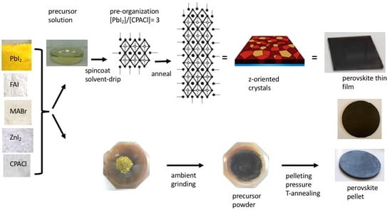
Figure 3.
Formation of films and pellets from their starting components. Decreasing ratio CPACl: FA/MA, annealing or grinding steps are indicated. The crystalline units form a larger well-organized and protected final product. See Reference [16] for more information on this composition.
Figure 3.
Formation of films and pellets from their starting components. Decreasing ratio CPACl: FA/MA, annealing or grinding steps are indicated. The crystalline units form a larger well-organized and protected final product. See Reference [16] for more information on this composition.

Figure 4.
Confocal microscopy image of FA0.85MA0.15Pb0.975Zn0.025I2.85Br0.15-[CPACl] obtained by dividing the photoluminescence lifetime-image by the intensity-image (INT) thereby accentuating the grain boundary areas, as processed with Image-J (lifetime/INT, fire-color coding). The network of light blue lines highlights the special grain boundary effect, which is in-fact induced by charge recombination interaction with the ITO surface (not observed on quartz). Pink spots are characterized by a very low emission intensity and long emissive lifetime. Image dimension is 20 × 20 μm. See also Reference [16]. This picture is best viewed on-screen.

Figure 5.
Field-emission scanning electron microscopy image of the perovskite doped with (from left to right) 0%, 5%, 10%, 15% Zn annealed at 80 °C (a), 100 °C (b) and 120 °C (c). MA(Pb:Zn)I3. Figure reprinted with permission from, Mater. Today Energy 2017, 5, 205–213, Reference [15].
Figure 5.
Field-emission scanning electron microscopy image of the perovskite doped with (from left to right) 0%, 5%, 10%, 15% Zn annealed at 80 °C (a), 100 °C (b) and 120 °C (c). MA(Pb:Zn)I3. Figure reprinted with permission from, Mater. Today Energy 2017, 5, 205–213, Reference [15].

Figure 6.
XRD spectrum of MA(Pb:Zn)I3-based thin films after incorporation of Zn2+ in concentrations of 0, 5, 10 and 15% (a). A shift of the peak representing the 110 plane is clearly visible in (b). Figure reprinted with permission from Mater. Today Energy 2017, 5, 205–213, Reference [15].
Figure 6.
XRD spectrum of MA(Pb:Zn)I3-based thin films after incorporation of Zn2+ in concentrations of 0, 5, 10 and 15% (a). A shift of the peak representing the 110 plane is clearly visible in (b). Figure reprinted with permission from Mater. Today Energy 2017, 5, 205–213, Reference [15].

Figure 7.
Binding energies of Pb 4f (a) and I 3d (b) which diminish upon increase of Zn2+ content. (c): Stretching vibration of the NH3+ group in pristine CH3NH3I and in perovskite. (d): Schematic representation of the lattice in which Zn2+ is incorporated. MA(Pb:Zn)I3-[Cl−]. Reproduced from Sustain. Energy Fuels 2018, 1093–1100, with permission from The Royal Society of Chemistry. Figure reprinted from Reference [13].

Figure 8.
EDS Elemental mapping of Zn atoms in the perovskite lattice. The Zn atoms are evenly dispersed over the structure and not aggregated at grain boundaries. MA(Pb:Zn)I3-[Cl−]. Reproduced from Sustain. Energy Fuels 2018, 1093–1100, Reference [13], with permission from The Royal Society of Chemistry.

Figure 9.
Changes of emission intensity (a) as well as emission decays (b) as a function of Zn(II) incorporation. MAPbI3-based material. MA(Pb:Zn)I3-[Cl−]. The optimum is at 3% for both graphs. Reprinted with permission from ACS Appl. Mater. Interfaces 2017, 9, 42875–42882, Reference [11]. Copyright 2017 American Chemical Society.


Table 1.
Photoluminescence lifetimes of different undoped and Zn(II) doped perovskite materials on glass or quartz (unless indicated). Additives are indicated in square brackets.
Table 1.
Photoluminescence lifetimes of different undoped and Zn(II) doped perovskite materials on glass or quartz (unless indicated). Additives are indicated in square brackets.
| Material | x (Zn) | τ (ns) Undoped (x = 0) | τ (ns) Doped | Reference |
|---|---|---|---|---|
| CsPb1-xZnxBr3 | <0.1 | 17 | 15 | [10] 1 |
| MAPb1-xZnxI3-[Cl−] | 0.03 | 74 | 154 | [11] |
| MAPb1-xZnxI3-[Cl−] | 0.001 | 10,740 | 12,910 | [13] 2 |
| MAPb1-xZnxI3 | 0.03 | 98 | 118 | [14] |
| MAPb1-xZnxI3 | 0.05 | 43 | 165 | [15] 3 |
| MAPb1-xZnxI3 | 0.10 | 43 | 247 | [15] 3 |
| MAPb1-xZnxI3 | 0.15 | 43 | 548 | [15] 3 |
| FA0.85MA0.15Pb1-xZnxI2.85Br0.15-[CPACl] | 0.025 | 7 | 12 | [16] 4 |
| FA0.85MA0.15Pb1-xZnxI2.85Br0.15-[CPACl] | 0.025 | - | 3.2; 8.5 | [16] 5 |
| MAPb1-xZnxI3-[Cl−] | 0.01 | 208 | 248 | [23] |
| FA0.85MA0.15Pb1-xZnxI2.85Br0.15 | 0.025 | 589 | 635 | [24] |
| FA0.85MA0.15Pb1-xZnxI2.85Br0.15-[CPACl] | 0.025 | - | 1548 | [24] |
| FA0.92MA0.08PbI3-[Cl−] | - | 364 | - | [25] |
| FA0.92MA0.08PbI3-[PEAI, Cl−] | - | 2835 | - | [25] |
| FA0.95MA0.05PbI2.85Br0.15 | - | 228 | - | [26] |
| FA0.95MA0.05PbI2.85Br0.15-[(I3)−] | - | 1105 | - | [26] |
1 Value of x is not exactly indicated, but is “low”, x < 0.1 for these nanoparticles in solution. 2 Lifetimes obtained with TPC (transient photo-current). 3 Average values on glass surface. 4 Average values on ITO surface. 5 Long components of emission of the center and grain boundaries of crystals on ITO surface. In References [14,15,26] we find no indication of chloride components used. PEAI is phenethylammonium iodide.
Table 2.
Reported power conversion efficiencies (PCE) for materials without zinc (undoped, ud) and Zn-doped (d) materials, together with their enhancement factors (d/ud). Compositions are estimated from their References. Additives are indicated in square brackets. A selection of certified world record efficiencies is given in the last seven entries.
| Material | x (Zn) | PCE (%) Undoped | PCE (%) Zn-Doped | d/ud | Reference |
|---|---|---|---|---|---|
| MAPb1-xZnxI3-[OAc−] | 0.016 | 7.27 | 9.69 | 1.33 | [9] 1 |
| MAPb1-xZnxI3-[Cl−] | 0.03 | 16.40 | 18.20 | 1.11 | [11] |
| MAPb1-xZnxI3-[Cl−] | 0.001 | 12.30 | 16.30 | 1.33 | [13] |
| MAPb1-xZnxI3 | 0.03 | 17.13 | 18.35 | 1.07 | [14] |
| MAPb1-xZnxI3 | 0.05 | 17.11 | 18.25 | 1.07 | [15] |
| MAPb1-xZnxI3-[Cl−] | 0.01 | 17.94 | 20.06 | 1.12 | [23] |
| FA0.92MA0.08PbI3-[PEAI, Cl−] | - | 23.32 | - | - | [25] 2 |
| FA0.95MA0.05PbI2.85Br0.15-[(I3)−] | - | 22.10 | - | - | [26] 3 |
| FA0.95MA0.05 PbI2.85 Br0.15 | - | 20.11 | - | - | [27] 4 |
| FA0.85MA0.15 PbI2.55 Br0.45 | - | 17.91 | - | - | [5] 5 |
| MAPbI3 | - | 3.81 | - | - | [28] 6 |
| FASnI3-[PEAI] | - | 9.00 | - | - | [29] |
| MASnIBr2 | - | 5.75 | - | - | [8] |
1 Average values of MA(63Pb:1Zn)I3 reported in Supporting info. 2 Record efficiency during part of 2018. 3 Record efficiency in 2017. 4 Record efficiency in 2015. 5 Record efficiency during part of 2014. 6 Record efficiency in 2009. In References [5,8,9,14,15,26,27,28,29] we find no indication of chloride components used in the precursor solutions.
© 2019 by the authors. Licensee MDPI, Basel, Switzerland. This article is an open access article distributed under the terms and conditions of the Creative Commons Attribution (CC BY) license (http://creativecommons.org/licenses/by/4.0/).
Share and Cite
MDPI and ACS Style
Kooijman, A.; Muscarella, L.A.; Williams, R.M. Perovskite Thin Film Materials Stabilized and Enhanced by Zinc(II) Doping. Appl. Sci. 2019, 9, 1678. https://doi.org/10.3390/app9081678
AMA Style
Kooijman A, Muscarella LA, Williams RM. Perovskite Thin Film Materials Stabilized and Enhanced by Zinc(II) Doping. Applied Sciences. 2019; 9(8):1678. https://doi.org/10.3390/app9081678
Chicago/Turabian StyleKooijman, Arjaan, Loreta A. Muscarella, and René M. Williams. 2019. "Perovskite Thin Film Materials Stabilized and Enhanced by Zinc(II) Doping" Applied Sciences 9, no. 8: 1678. https://doi.org/10.3390/app9081678
Note that from the first issue of 2016, this journal uses article numbers instead of page numbers. See further details here.