1. Introduction
During the last decades, an increasing research interest has been directed toward a variety of satellite services provided in the Ku-band frequency range, e.g., digital radio, TeleVision (TV) broadcasting, and broadband Internet. Moreover, new microwave communication systems designed for automotive, high velocity trains, boats, airplane radio navigation, 5G wireless, smart city, and industry 4.0 applications constitute a current research hot topic. In all of the aforesaid cases, the development of high-performance antennas can significantly contribute to increase the overall information capacity of an innovative communication system. Efficient satellite communication in the Ku-band requires antennas with high gains and a broadband of at least 2 GHz, from 10.5 to 12.5 GHz. High performance, flat-shaped, and wall-mounted antennas that have been optimized with the aim of reducing the environmental and/or visual impact, are promising devices. Patch antenna elements are largely utilized in the fabrication of high-performance arrays. Unfortunately, as patches resonate at a single frequency, they typically exhibit a narrow relative bandwidth of about 2%; this is a strong drawback that prevents their usage in wide-band applications.
There are various approaches to enhance the bandwidth including the employment of suspended substrates, multi-stack [
1,
2,
3], and metalized baking cavities [
4,
5,
6,
7].
Substrate integrated waveguide (SIW) technology has been largely employed for the construction of couplers, filters, oscillators, amplifiers, mixers, in addition to antennas since it allows for low-cost implementation, fast prototyping, and precise manufacturing [
8,
9,
10,
11,
12,
13,
14,
15,
16,
17,
18,
19]. It can be used to improve the antenna radiation characteristics, thus obtaining better performances than those of the conventional microstrip/printed board circuits (PCB) while maintaining the typical advantages of planar technologies. In fact, SIW technology allows for low cost, lightness, easy integration with both passive and active devices, high power levels, feasible mass production, and manufacturing repeatability. Several SIW cavity-backed antennas and feeding geometries have been reported in the literature [
16,
17,
18,
19,
20,
21,
22,
23,
24,
25]. For example, a reconfigurable SIW Cavity-Backed Slot (SIW-CBS) antenna with a one octave tuning range and six different tuning states was presented in [
16]. A new tuning method based on loading the SIW cavity with shortening posts and manipulating the field distribution within the cavity was proposed. In [
17], a SIW-slot feeding structure was introduced in a fully substrate-integrated thin Fabry-Pérot cavity (FPC) antenna in order to achieve boresight radiation free of beam squint and low backward radiation levels. Moreover, a single patch with truncated corners has been developed to provide a linear polarized antenna in SIW technology for the Ku-band range of frequency [
18]. This technology has been recently proposed as an example in the 57–71 GHz band for 5G [
23], X-band [
24], and dual-band in K-band [
25] applications.
In this paper, a broadband SIW cavity-backed microstrip patch antenna was designed and optimized for radiation in the Ku band. Starting from the antennas reported in [
18,
26,
27], the patch geometry has been enhanced by introducing lateral cuts and asymmetric feeding of each single radiating element to obtain a wider operation band and frequency downshift. This means that the radiating elements are smaller, allowing more space for the feeding network and improving the isolation among transmission lines. In addition, the particular shape of the radiating element allows for the use of a simpler matching network to the feeding line. A 16 × 16 element array was designed and fabricated to obtain a pre-prototype antenna. In particular, the radiating element spacing was optimized to minimize the secondary grating lobes while using the maximum allowable space in the substrate backplane. The single element antenna as well as the antenna arrays were fabricated by using two substrates (top and bottom ones) of the same material and different thicknesses. The top substrate contained the feeding network and patches. Each patch element of the array was coupled with an optimized SIW cavity (backed) lying in the bottom substrate. At first, simple screws were employed to connect the two substrates. In the final prototypes, a prepreg press compression molding process was employed to stack the multi-layer PCB. The design was performed by employing the CST Microwave Studio© software, and the SIW antenna prototypes were fabricated with the PCB process in the SOMACIS plant. A complete feasibility investigation is illustrated by reporting all of the steps toward the 16 × 16 antenna array optimization. Excellent characteristics, comparable or slightly better than those reported in [
18,
26], were obtained. In particular, the same gain but with a wider band compared with [
26], was obtained when the same number of array elements was considered. The 16 × 16 antenna array exhibited high gain, close to G = 29.2 dBi, and good return losses in a wide frequency region including the whole Direct Broadcast Satellite (DBS) band (i.e., in the range 10.7–12.7 GHz) and over. A practically squint-less main lobe was measured. Therefore, a 16 × 16 antenna array could be of practical interest in actual communication systems. Different materials have been considered in order to choose the best trade-off between the engineered prototypes.
The paper is organized as follows.
Section 2 presents the design of the single cavity backed antenna;
Section 3 shows the design of the antenna arrays;
Section 4 describes the fabrication and the characterization of the prototypes;
Section 5 details the feasibility and discussion on the material choice; and
Section 6 presents our conclusions.
2. Single Antenna Design
The design of high-performance antennas requires several trade-offs. High permittivity substrates can allow the construction of very compact microstrip antennas. Thick substrates with lower dielectric constants offer a better radiation efficiency and wide bandwidth, but larger sizes are needed. Further performance improvements can be obtained by employing SIW circular cavities backing the microstrip patch antennas. They also allow the suppression of surface waves, thus obtaining very high isolation from the surrounding elements of antenna arrays.
In this paper, a low-loss and low dielectric constant substrate was used. In particular, the Rogers Duroid 5880 with a dielectric constant of ε
rs = 2.2 and loss tangent of δ = 0.0009 was chosen for both (top and bottom) substrates. Among the Rogers Duroid 5880 commercially available substrates, the top substrate (on which the patch antennas were obtained via etching) had a thickness of h
s = 0.381 mm and the bottom one (including the cavity walls) had a thickness of h
c = 1.575 mm; the metal layers of both substrates were h
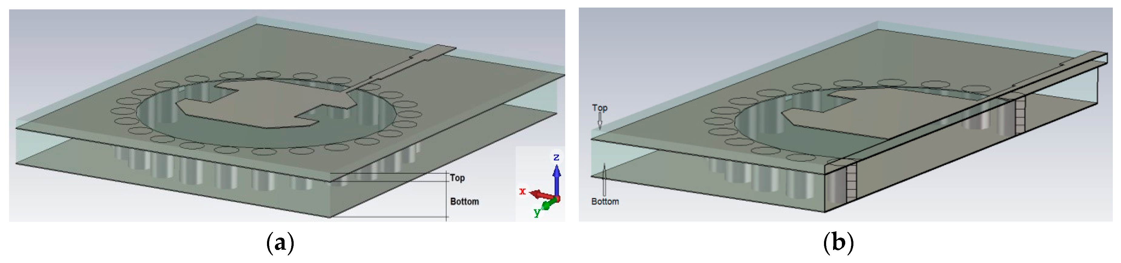
m = 0.035 mm thick. Metalized via holes circularly spaced constitute the SIW cavity side walls, as shown in
Figure 1a, which illustrates a global view, and
Figure 1b shows a section view of the single antenna.
The design was performed by using the 3D commercial software tool CST Microwave Studio©. Several simulations were performed to reach the best trade-off in terms of insertion loss reduction, bandwidth broadening, and radiation pattern characteristics.
The proposed antenna combined the attractive features of both cavity-backed patch antennas and patch antennas with truncated corners. Moreover, as a further improvement with respect to [
18,
26,
27], two suitable cuts on the sides of the rectangular patch were designed to provide a wider frequency band and a frequency downshift. The radiating element is then smaller, allowing a more compact size of the whole array.
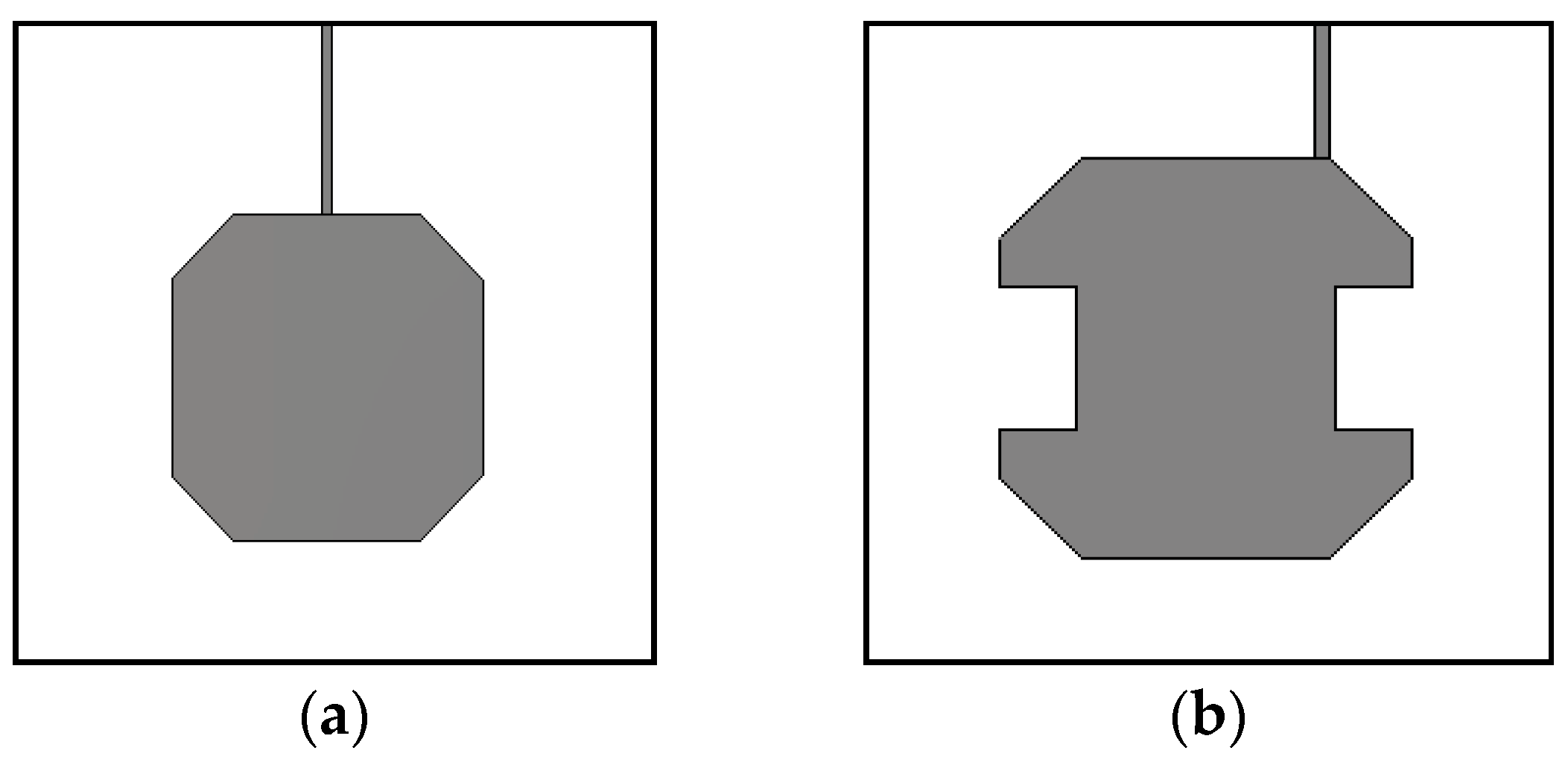
In order to identify the different contributions, a patch antenna without a backing cavity and with the feed located in the center is shown in
Figure 2a.
Figure 2b shows the modified patch obtained by performing suitable lateral cuts and by moving the feeding microstrip in the corner of the patch. Both patches had a side b = 7.7 mm, and a substrate thickness h
s = 0.381 mm with a metal thickness of h
m = 0.035 mm.
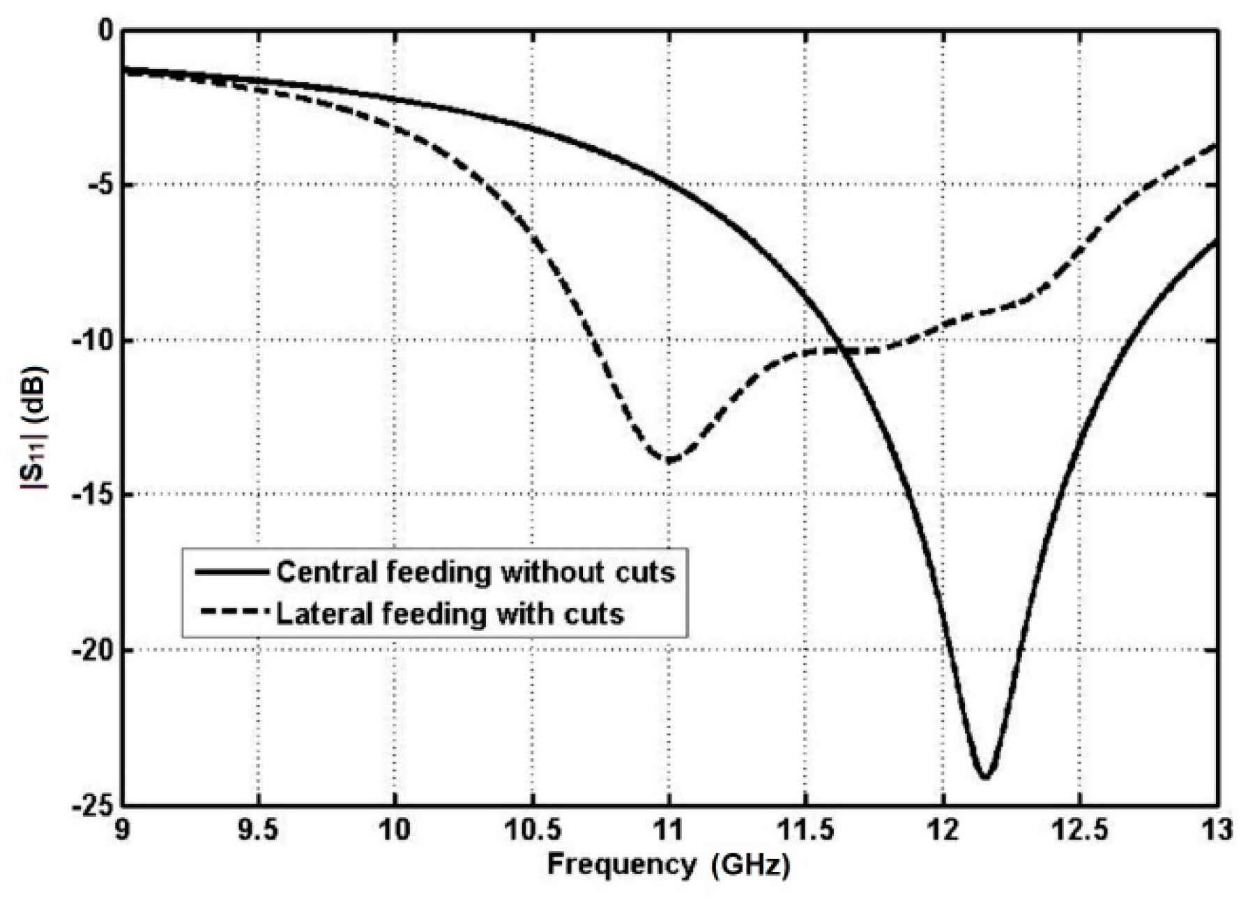
The comparison between the modulus of the scattering parameter S
11 of the antenna illustrated in
Figure 2a (solid curve) and the modulus of the scattering parameter S
11 of the antenna illustrated in
Figure 2b (dashed curve) is reported in
Figure 3. For the antenna with a lateral cut and feeding strip line in the corner, the minimum of the modulus of the scattering parameter S
11 shifted toward the lower frequency of about 1 GHz with respect to that of the antenna without a lateral cut and central feeding. The −10 dB bandwidth slightly increased (about 0.1 GHz), changing from 11.6–12.6 GHz to 10.7–11.8 GHz.
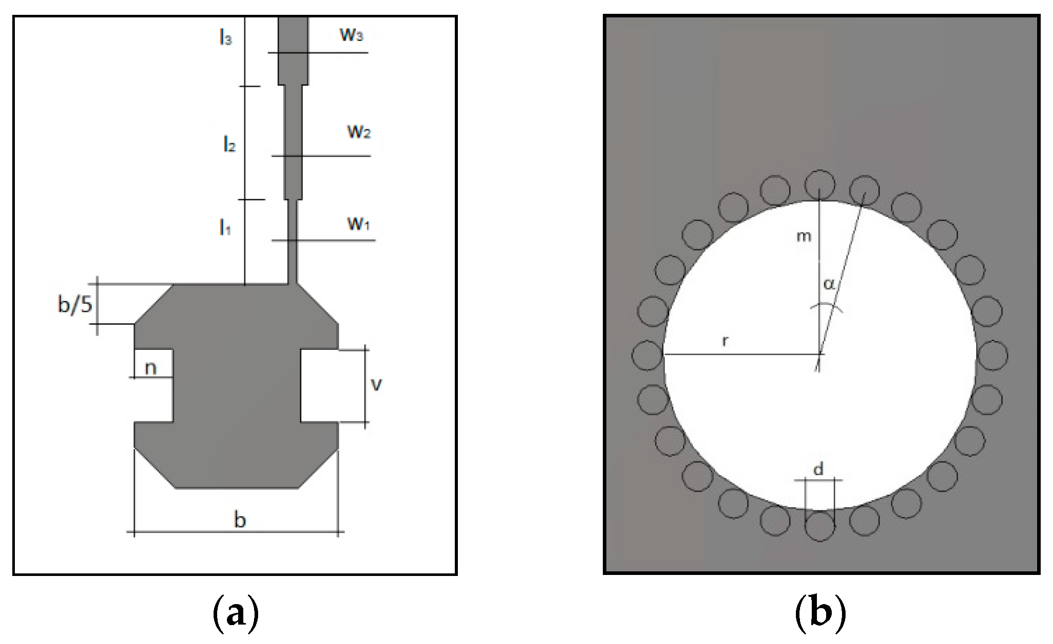
A suitable SIW cavity backing the patch antenna was designed. The optimized antenna patch parameters are shown in
Figure 4, illustrating the top view of (a) the top layer and (b) the bottom layer, and are listed in
Table 1.
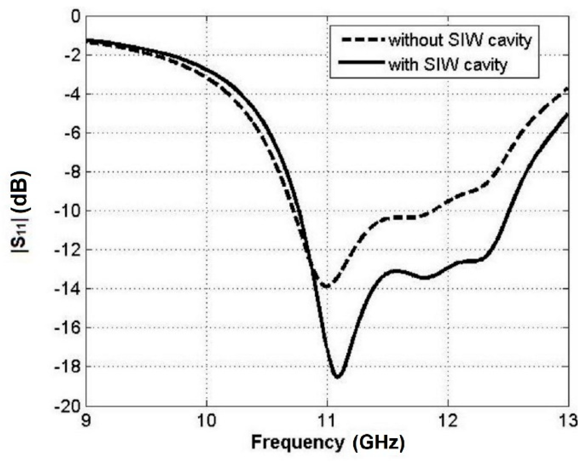
The effect of the SIW cavity backing on the antenna performance is illustrated in
Figure 5. The modulus of the S
11 parameter for the patch antenna with lateral cut and feeding in the corner was reported for both cases: without (dashed curve) and with (solid curve) SIW cavity. The bandwidth for the antenna with SIW cavity was about 2 GHz and covered the whole satellite communication Ku band. It is worthwhile noting (see
Figure 3 and
Figure 5) that the broadband operation was obtained by a proper design of both the patch antenna with lateral cut and feeding line in the corner and SIW cavity.
The designed single element geometry is simpler with respect to other interesting cavity backed antennas reported in the literature, requiring sophisticated matching sections [
19]. Moreover, a circular polarization could be obtained with slight patch shape changes.
3. Antenna Array Design
The most widely-used techniques for feeding microstrip patch arrays can be categorized into two main kinds: the series and the corporate (parallel) ones. Corporate feeding has a single input port and multiple feed lines arranged in parallel. Each line is terminated with an individual radiating element, e.g., a patch antenna. The basic corporate feed is composed of two-way power dividers, which can be either 3 dB splitters or dividers with different power at the output ports.
In this paper, the corporate feeding with 3 dB splitters was used, since it allows a feed with the same amplitude and phase of each radiating element. One drawback is that for long feeding lines, insertion losses cannot be negligible, this reducing the array efficiency. Arrays of uniform antennas consist of a repetition of radiating elements in a regular fashion. Each element is also located at a specific distance from the other.
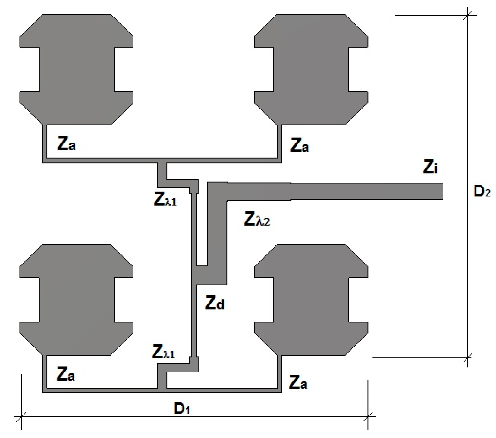
Figure 6 shows the base cell antenna employed in this paper to obtain the array and made by 2 × 2 patch antennas (four elements) spaced next to each other at 0.66 × λ
0 in both directions of the array plane, where λ
0 is the wavelength in vacuum at the central frequency of the Ku band f = 11.7 GHz, so that D
1 = D
2 = 25.2 mm. The input impedance of the antenna Z
a = 94.90 Ω was matched to the line of the first two-way power divider. A quarter-wave transformer with Z
λ1 = 67.10 Ω was used to match the lines with characteristic impedance Z
a (matched to the single radiating element) with the line of characteristic impedance Z
d = 47.45 Ω. The quarter-wave transformers with Z
λ2 = 48.70 Ω were designed to match the line with characteristic impedance Z
d with the input line with Z
i = 50 Ω.
A larger planar array can be obtained as a regular repetition in the horizontal and vertical directions of the base cell layout of
Figure 6. Following this approach, we designed the 4 × 4, 8 × 8, and 16 × 16 antenna arrays.
4. Antenna Fabrication and Characterization
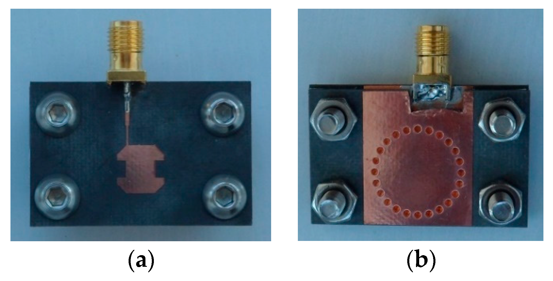
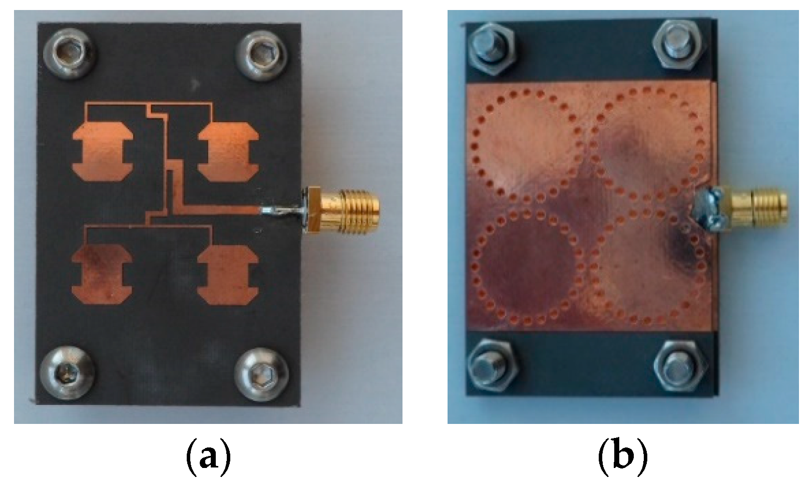
The single antenna prototype, manufactured by SOMACIS Spa, using a Rogers Duroid 5880 substrate with a dielectric constant ε
rs = 2.2 and loss tangent δ = 0.0009, is shown in
Figure 7. The top view (
Figure 7a) and the bottom view (
Figure 7b) are depicted. To keep the electrical continuity between the top layer and the bottom layer, four external screws were used.
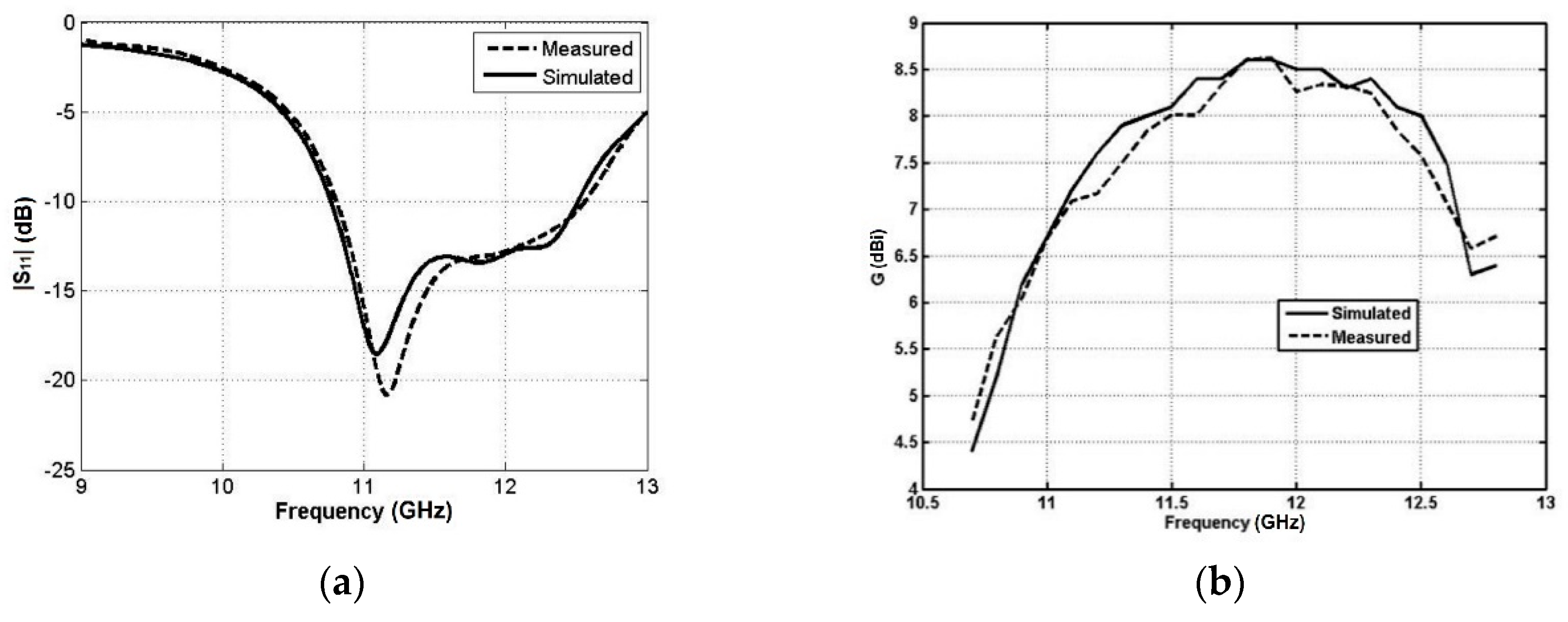
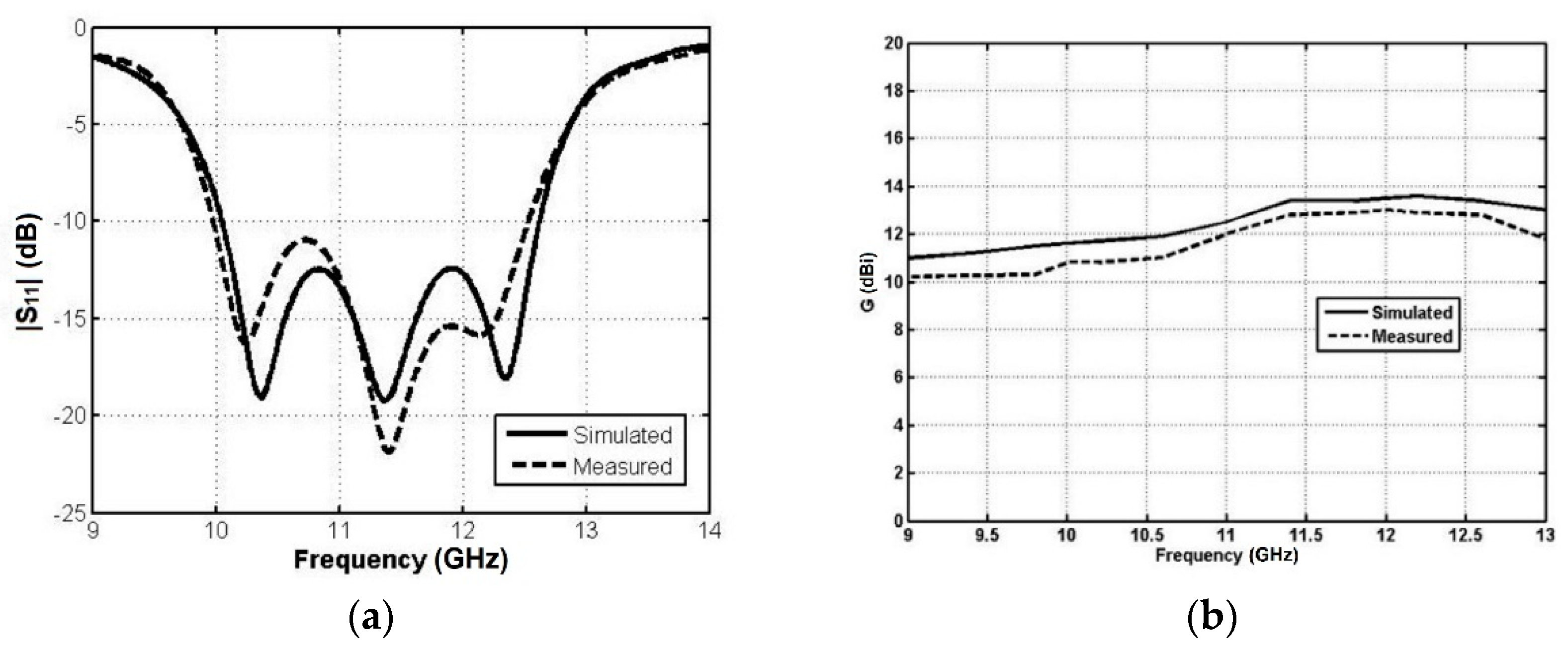
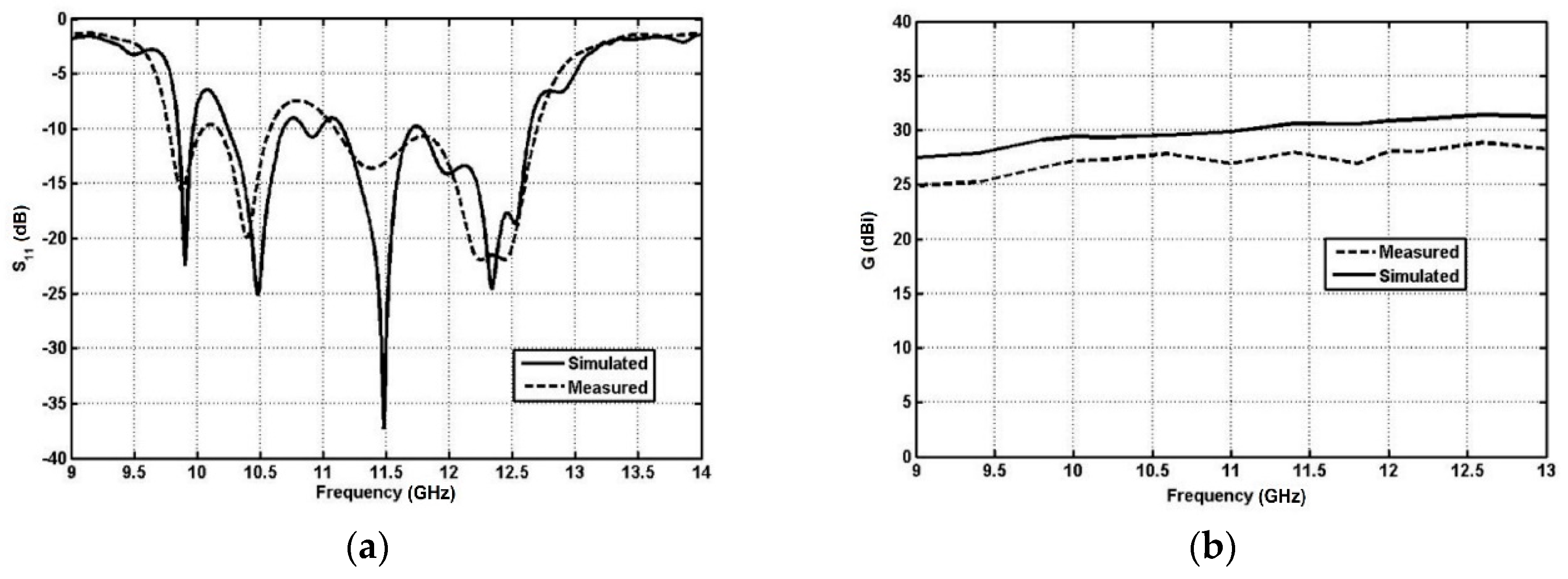
Figure 8a illustrates the simulated (solid curve) and measured (dashed curve) modulus of the S
11 scattering parameter of the single SIW cavity backed antenna. The measured and simulated curves were in good agreement in the overall Ku bandwidth (10.7–12.7 GHz). The measured −10 dB bandwidth was about 2 GHz, as expected.
Figure 8b illustrates the simulated (solid curve) and measured (dashed curve) gain G of the SIW cavity backed antenna versus the frequency. The gain of the antenna was higher than 6.8 dB in the frequency band 10.7–12.7 GHz. The maximum gain G = 8.6 dB occurred at the frequency f = 11.7 GHz.
Figure 9 shows the prototype of the 2 × 2 antenna array (base cell).
Figure 10a illustrates the simulated (solid curve) and measured (dashed curve) modulus of the S
11 scattering parameter.
Figure 10b shows the gain versus the frequency. The measured maximum gain is G = 13 dBi close to the frequency f = 12 GHz. The slight difference, less than 1.2 dBi, between the simulated and measured gain curves in the Ku band was due to both the power leakage of the feeding network and the substrate losses, which could be slightly different with respect to the values used in the simulation. As for the previous case, the good agreement between the simulated and the measured curve was apparent overall in the Ku bandwidth. The −10 dB bandwidth was about 2.5 GHz.
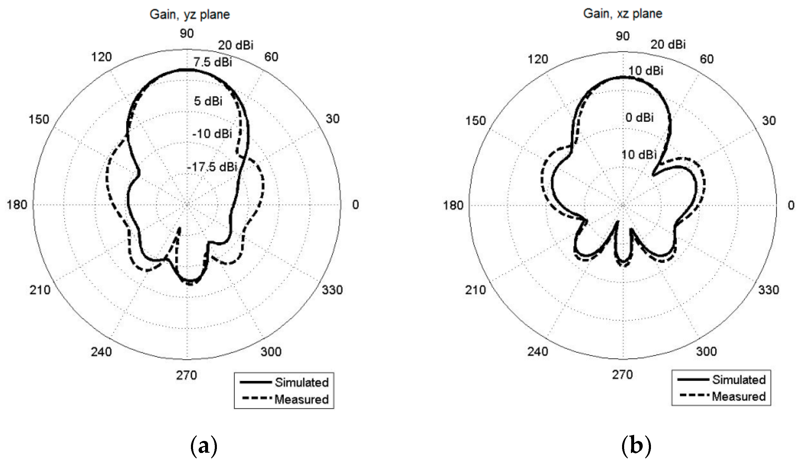
For the prototype of the 2 × 2 antenna array,
Figure 11a,b show the simulated (solid curves) and measured (dashed curves) gain G, at the frequency f = 11.7 GHz, in azimuth y-z plane and in elevation x-z plane, respectively. The half power beam width HPBW = 37.8° was measured at the frequency f = 11.7 GHz in the azimuth y-z plane. The radiation pattern and gain measurements were performed with StarLab Antenna Measurement Systems-Satimo©.
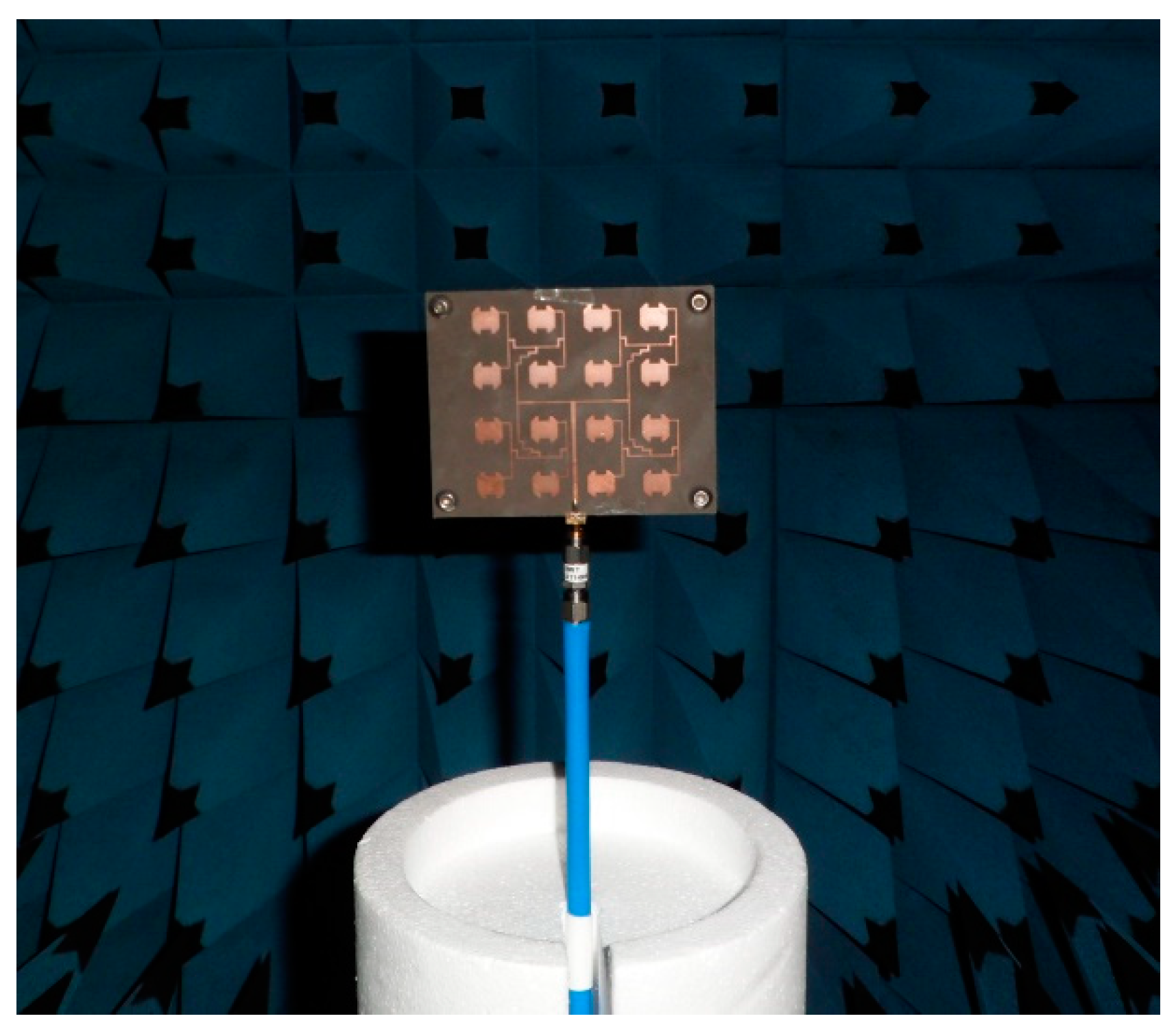
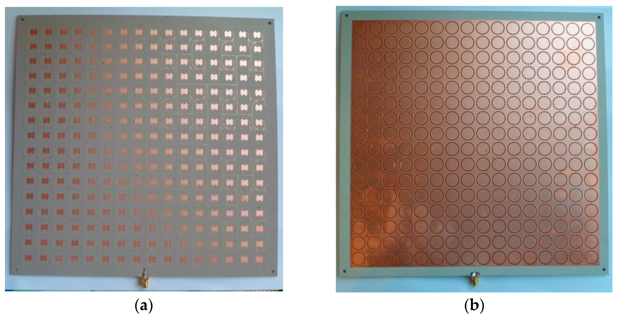
The 4 × 4 array was constructed, see the prototype in
Figure 12, by repeating the 2 × 2 base cell in both the x and y directions; then characterized, see
Figure 13, which illustrates the anechoic chamber.
The measured (dashed curves) and simulated (solid curves) gain G pattern in the azimuth y–z plane and in the elevation x–z plane are reported in
Figure 14a,b, respectively. In both cases, the figures show good agreement between the simulation and measurement. As expected, by increasing the number of the array elements, a narrower shape (pencil like) of the radiating main lobe occurred. In fact, for the 4 × 4 array, a half power beam width (HPBW) of 19.6° at the frequency f = 11.7 GHz was measured.
The simulated (solid curve) and measured (dashed curve) gain for the 4 × 4 array versus the frequency is illustrated in
Figure 15. The highest measured gain was G = 18.7 dBi at a 12.5 GHz.
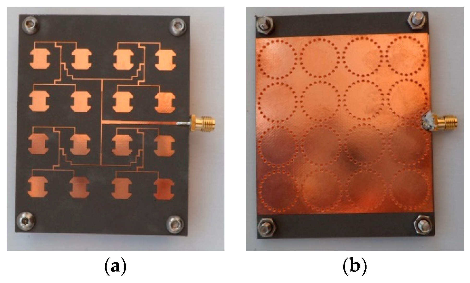
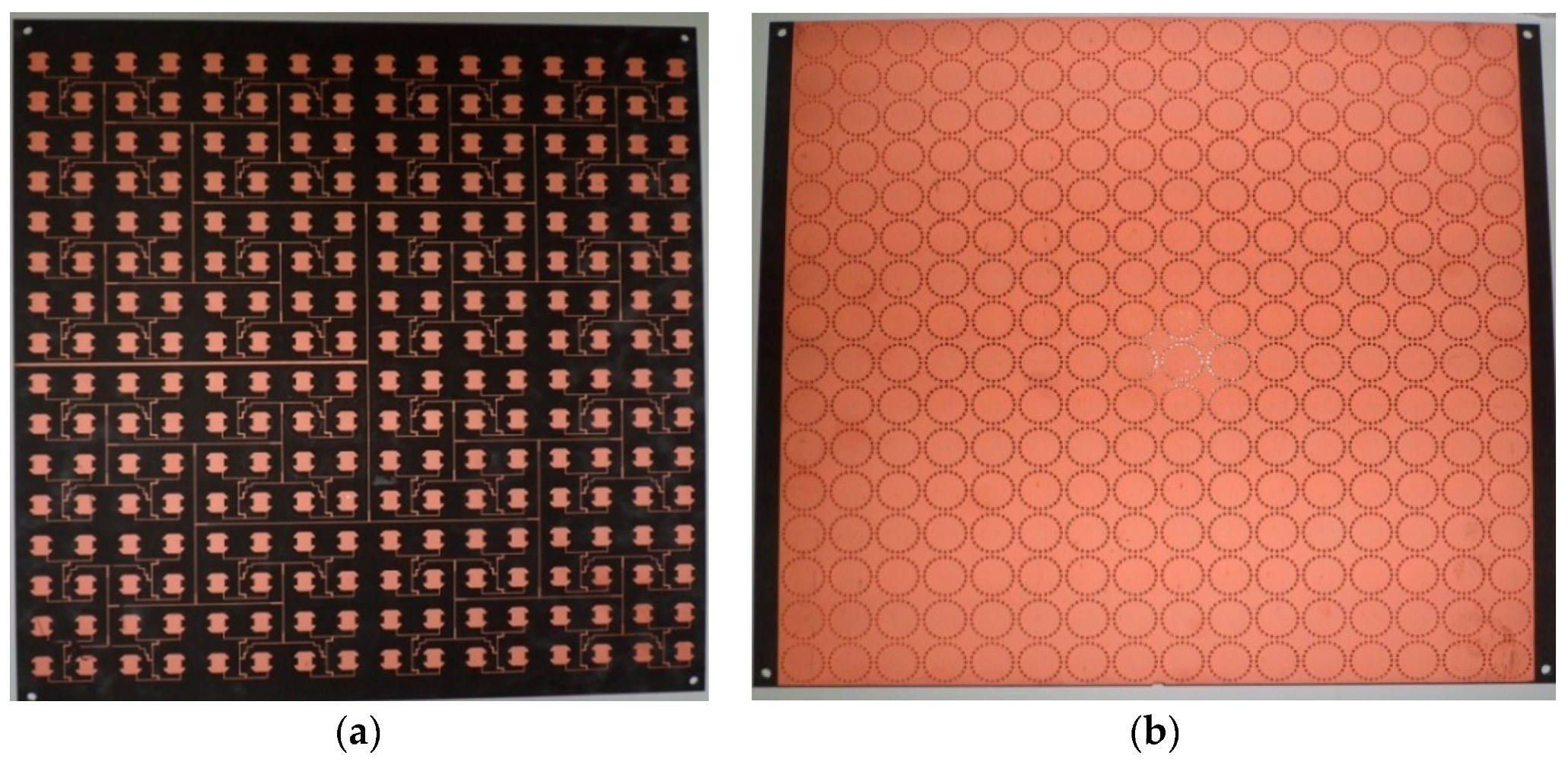
The 8 × 8 antenna array was constructed as seen in the prototype shown in
Figure 16.
Figure 17a shows the simulated (solid curve) and measured (dashed curve) modulus of the S
11 scattering parameter versus the frequency for the 8 × 8 antenna array. A −10 dB bandwidth was about 3. A little ripple of the measured modulus of the S
11 scattering parameter occurred close to the frequency f = 10.55 GHz and is most likely due to the thin air gap between the two layers fixed with external screws. A similar ripple can be obtained via simulation by considering an air gap g = 0.068 mm. This problem can be avoided by integrating the two layers via a prepreg/press procedure. In
Figure 17b, a difference of about 1.7 dBi between the simulated and measured gain occurred. The difference between the simulated and measured gain was due to the manufacturing tolerance. For the 8 × 8 antenna array, the measured maximum gain was G = 23.8 dBi at a 12.5 GHz. The gain G is practically coincident with the results reported in [
26] while the bandwidth 9.5–12.7 GHz almost doubled with respect to the antenna reported in [
26]. The radiation gain of the array 8 × 8 in the y–z and x–z planes is shown in
Figure 18a,b, respectively. The half power beam width in the azimuth y–z plane measured at a frequency of 11.7 GHz was HPBW = 9.5°. The maximum gain of the main lobe at the frequency f = 11.7 GHz was G = 22.6 dBi, the first side lobe level was −12.9 dBi.
In actual satellite application, a gain of about G = 30 dBi and a band of at least 2 GHz is required. A wider bandwidth is welcome to increase the communication capacity. To definitively prove the practical interest toward this kind of antenna [
18,
26,
28,
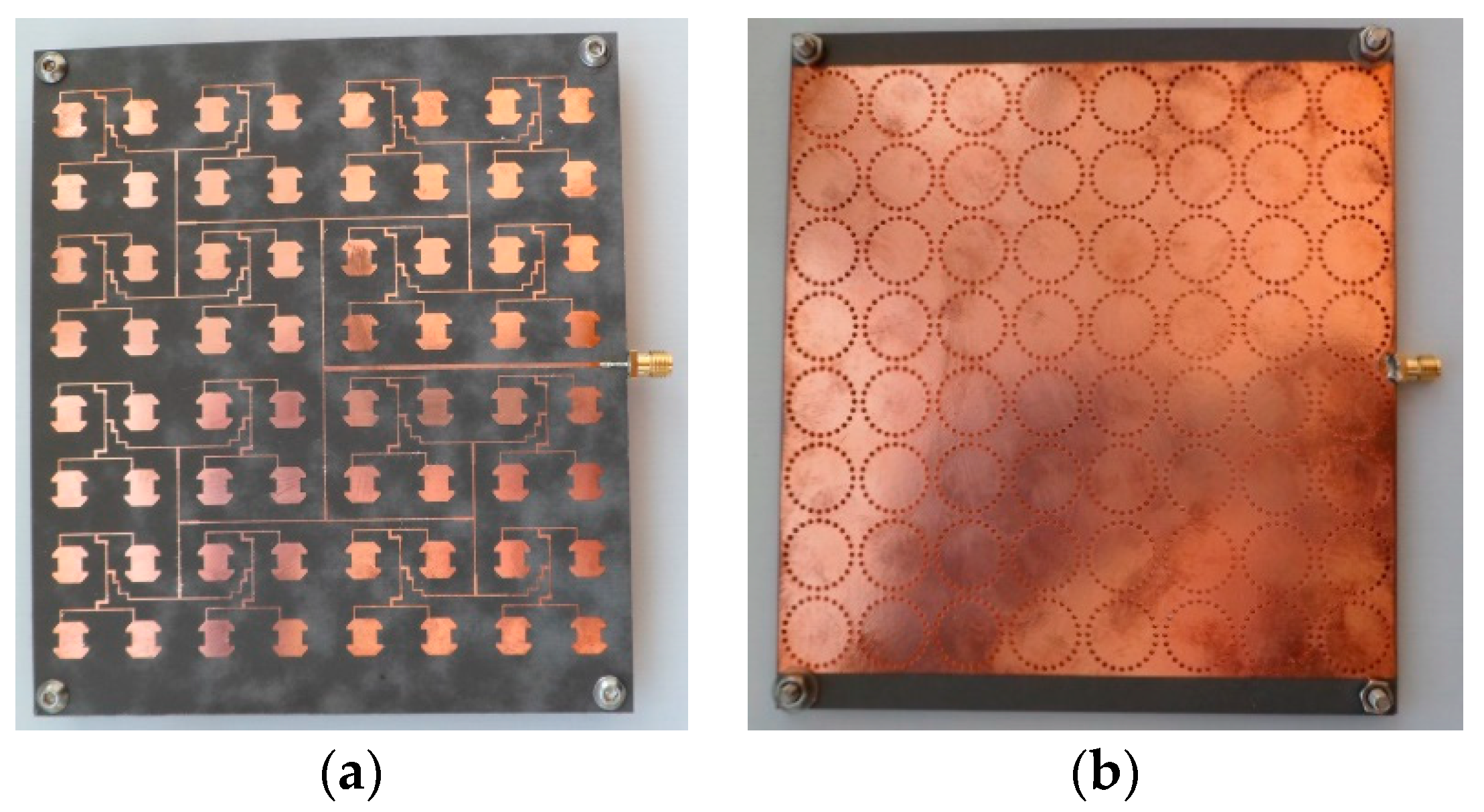
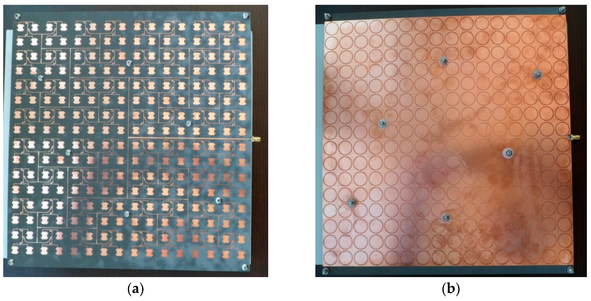
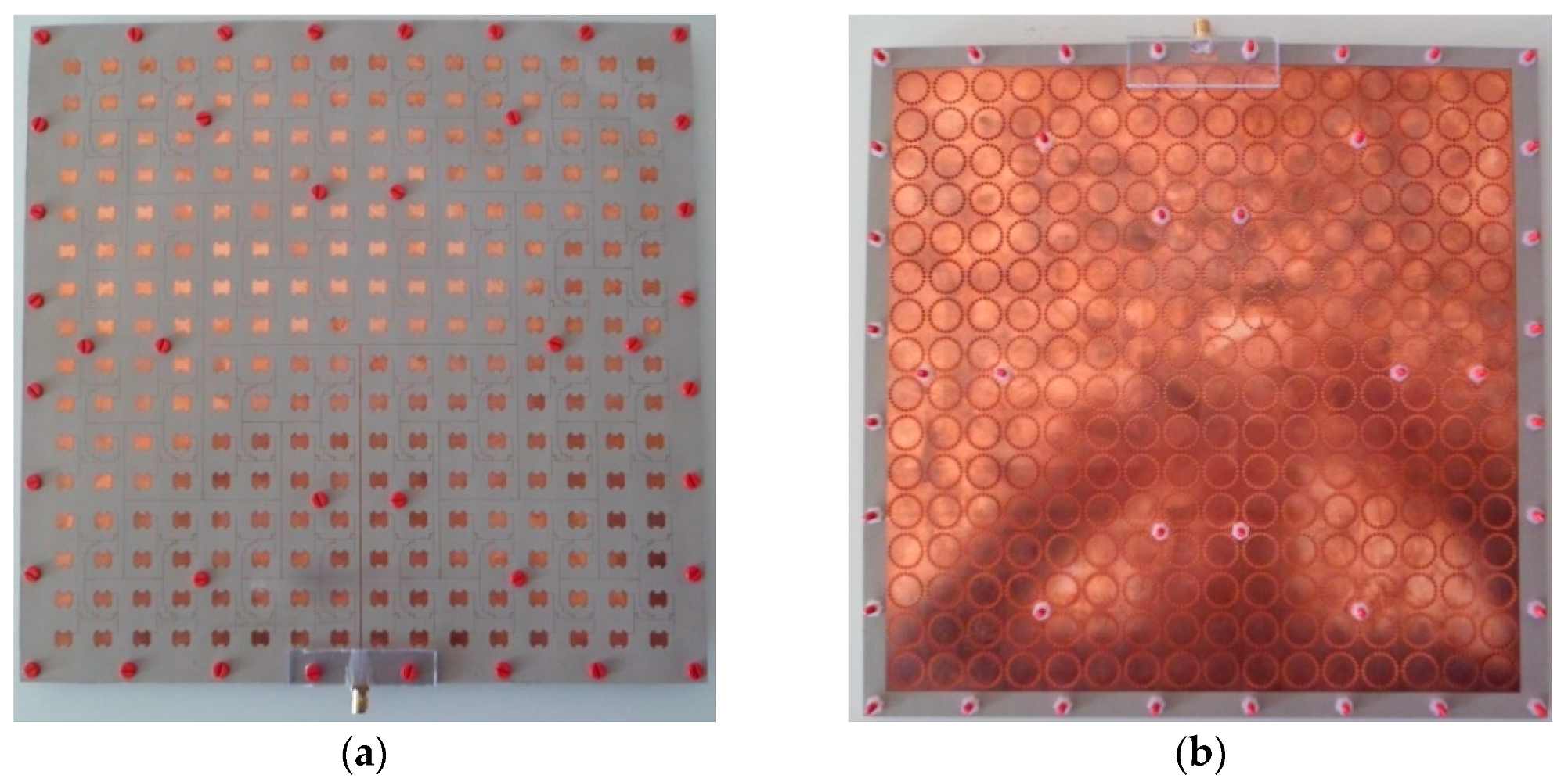
29] the investigation was further extended and an array with 256 elements (16 × 16 array) was built (see the prototype of
Figure 19).
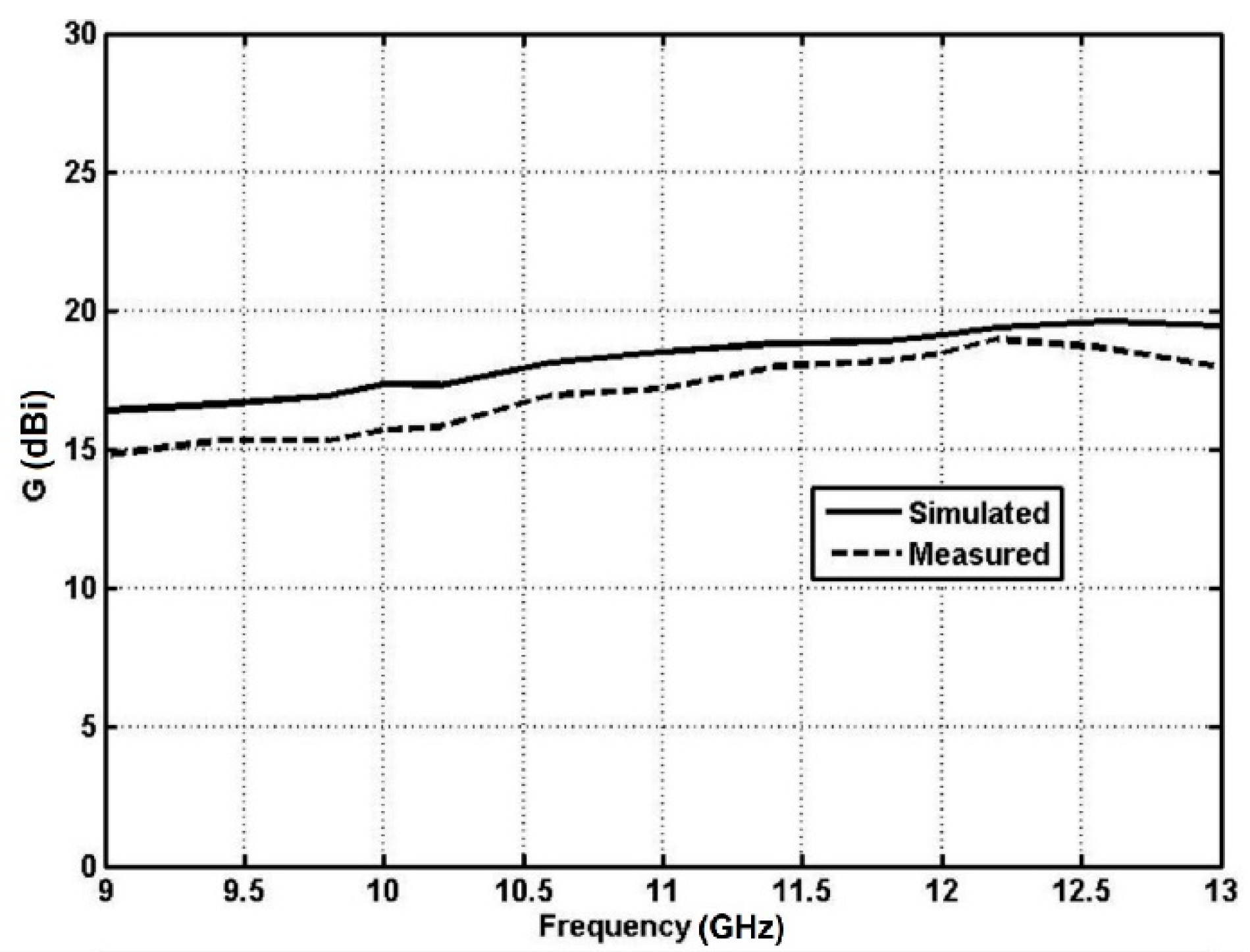
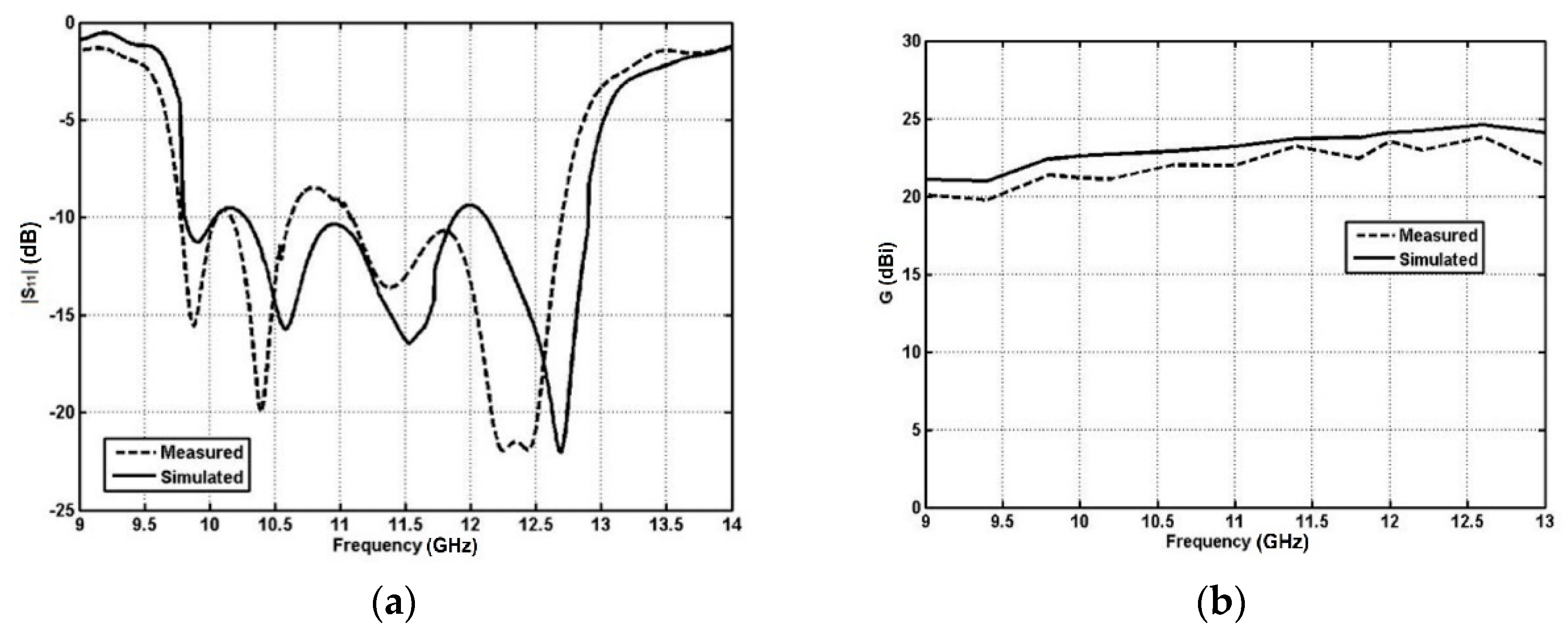
Figure 20a shows good agreement between the simulated and measured S
11 in a very wide range of frequencies (at −10 dB, the range was about 9.8–12.6 GHz). A flat behavior of the measured and simulated gain, with a difference of about 2.4 dBi between the two curves, is apparent in
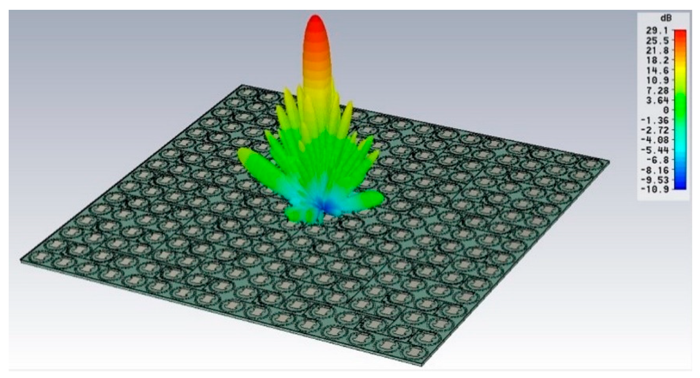
Figure 20b. The maximum gain value measured was obtained at a frequency of 12.6 GHz and it was close to G = 29.2 dBi. The simulated 3D radiated gain at a frequency of f = 11.8 GHz obtained with CST Microwave Studio© is shown in
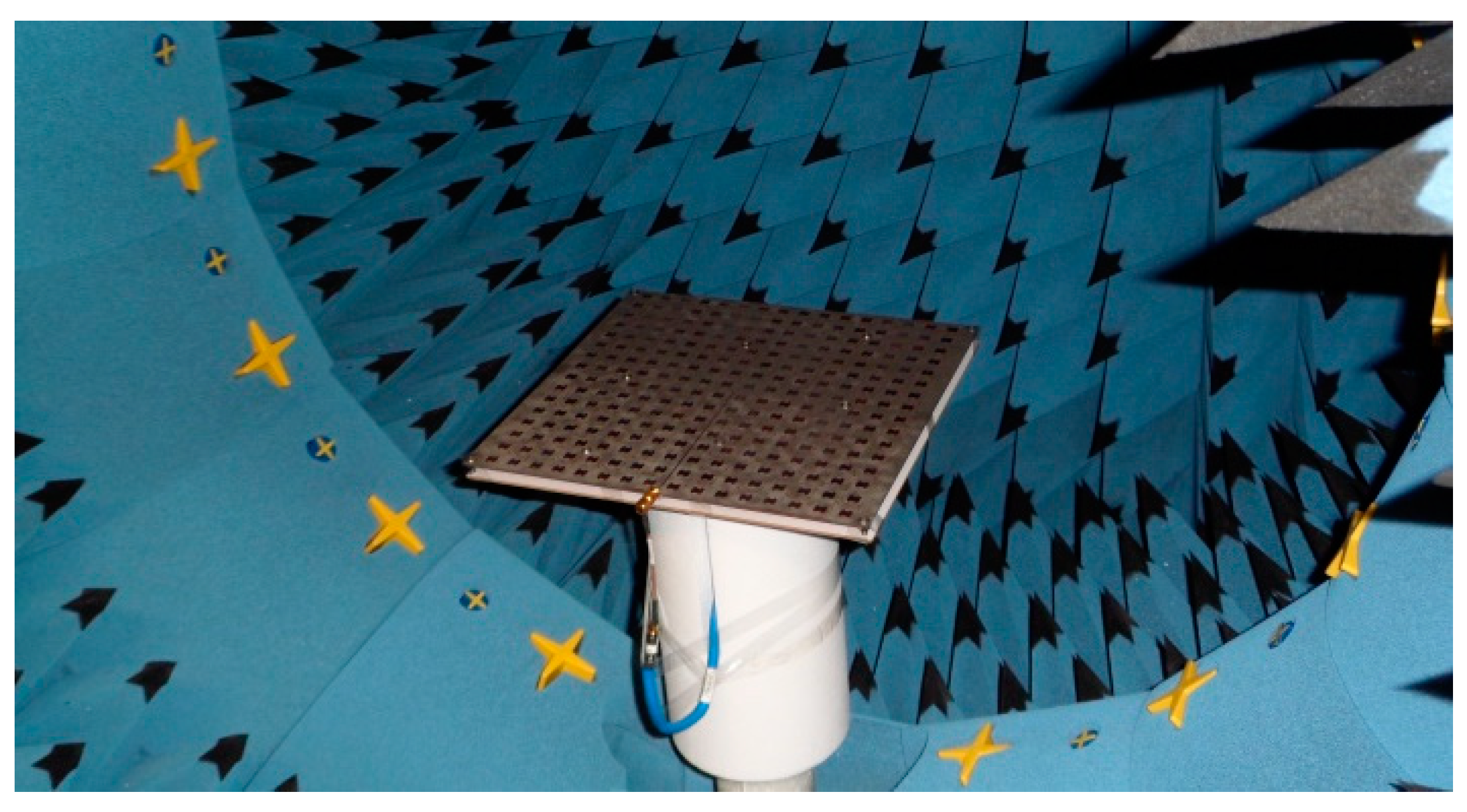
Figure 21, the maximum simulated gain was G = 30.59 dBi. The radiated gain measurement was made with a StarLab Antenna Measurement Systems-Satimo© anechoic chamber as shown in
Figure 22.
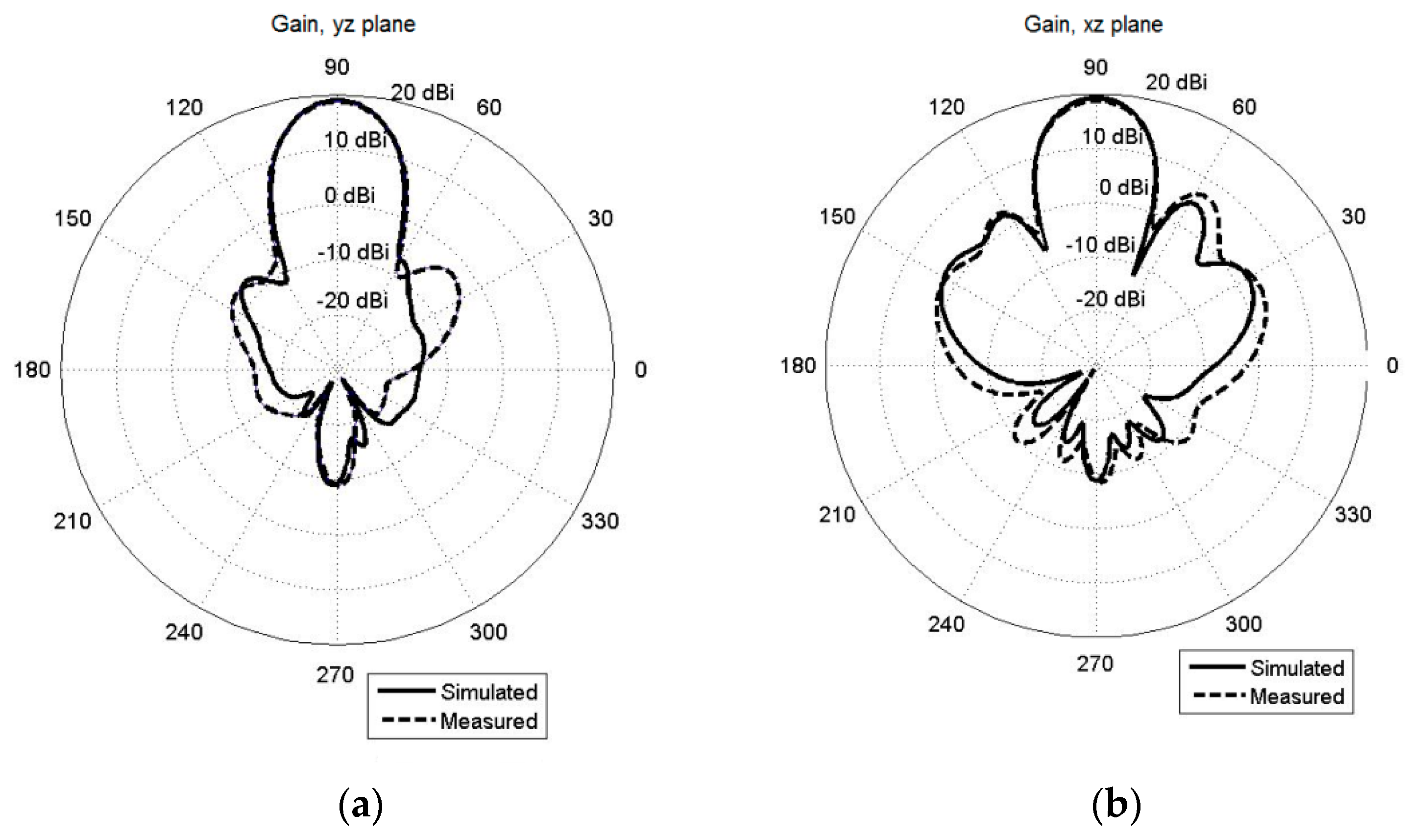
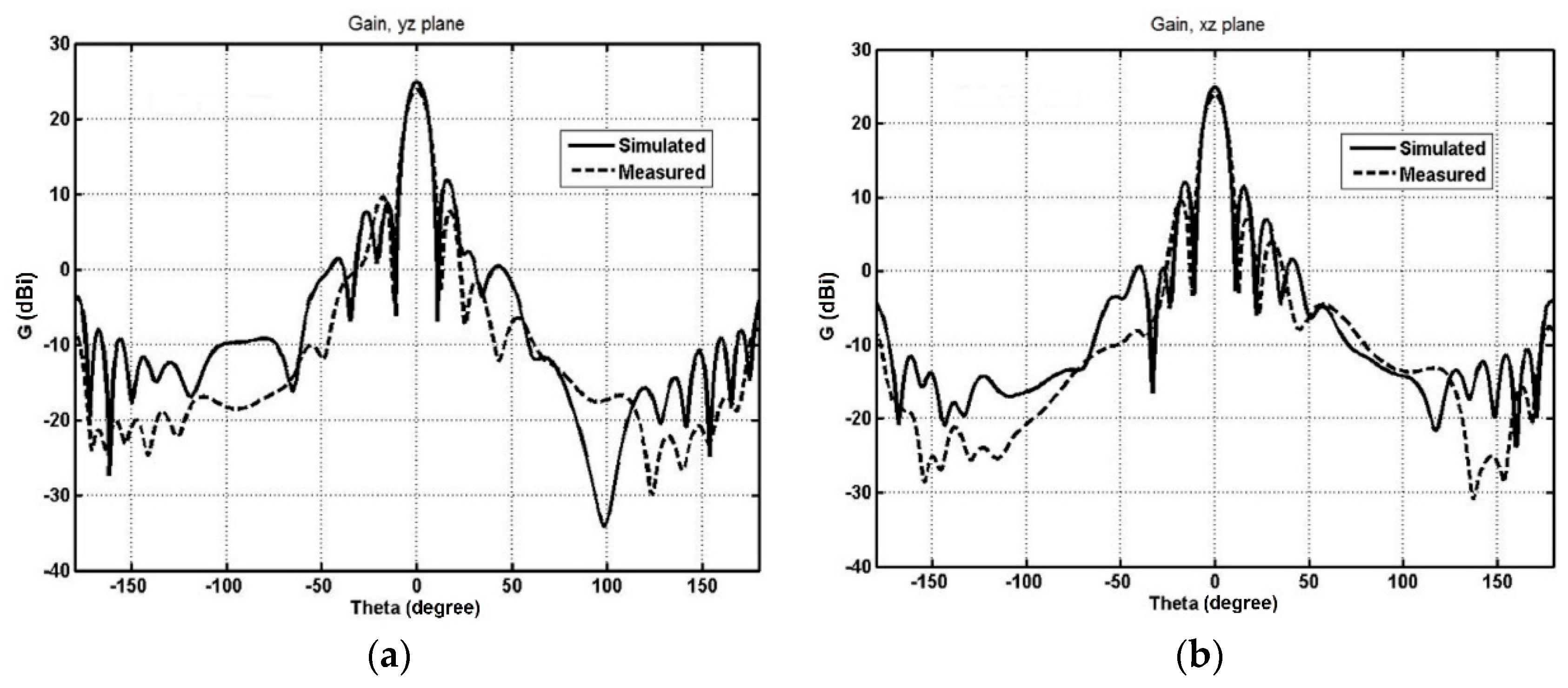
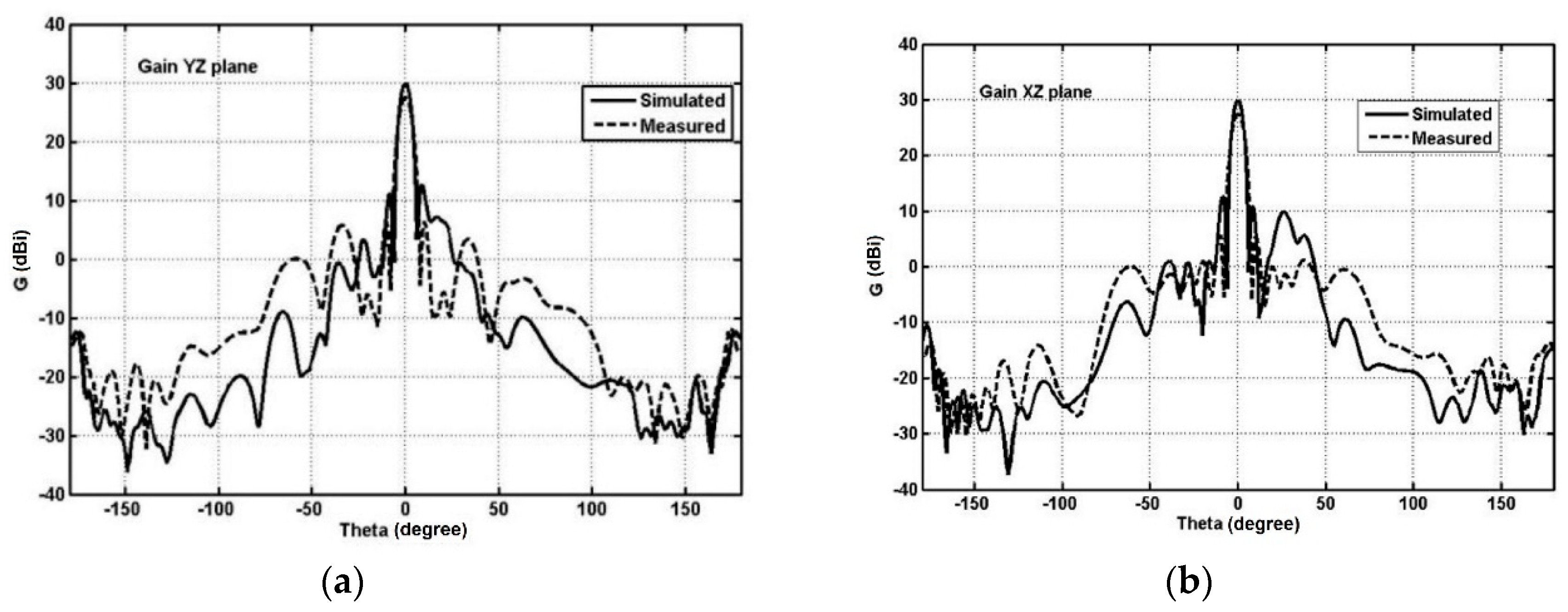
Figure 23a,b show the agreement between the simulated and measured gain G in azimuth y–z plane, and in elevation x–z, respectively, at a frequency of f = 11.8 GHz. A half power beam width (HPBW) of 4.8° was measured at a frequency of 11.8 GHz in the azimuth y–z plane. The measured gain at a frequency of f = 11.8 GHz was 26.8 dBi.
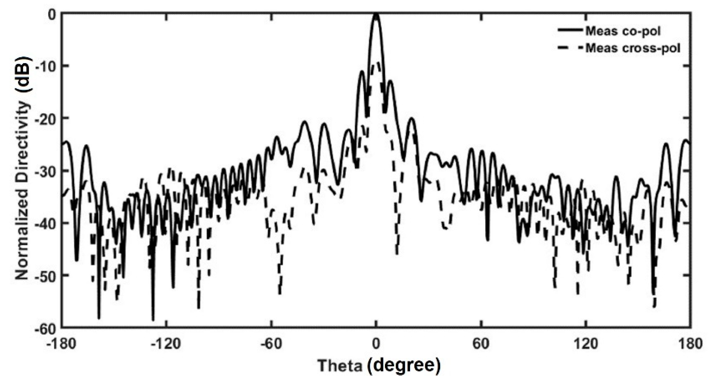
Figure 24 shows the cross polarization of the 16 × 16 array. The measured cross-polarization at a frequency of f = 11.8 GHz was −10 dB.
By increasing the number of the array elements, the insertion losses due to the larger feeding network and the coupling among the feeding lines and the radiating elements cannot be neglected. In fact, by increasing the number of array elements, the antenna radiation efficiency decreases. In particular, the measured efficiencies for the 2 × 2, 4 × 4, 8 × 8, and 16 × 16 arrays were 93%, 89%, 69%, and 52%, respectively, at a frequency of 11.7 GHz where the maximum gain was obtained. Even if these values are larger with respect to those reported in [
26], the efficiency behavior was confirmed.
By considering the beam shape, the negligible main lobe squint and the other measured characteristics, these planar antenna arrays seem very promising and are feasible for applications in the field of satellite communication.

 ,
, 


