Study of Implantation Defects in CVD Graphene by Optical and Electrical Methods

Institute of Electronic Materials Technology, Wolczynska 133, 01-919 Warsaw, Poland
*
Author to whom correspondence should be addressed.
Appl. Sci. 2019, 9(3), 544; https://doi.org/10.3390/app9030544
Submission received: 26 December 2018
/
Revised: 28 January 2019
/
Accepted: 31 January 2019
/
Published: 6 February 2019
(This article belongs to the Special Issue Novel Insights to Raman Spectroscopy: Advances and Prospects)
Abstract
:Featured Application
graphene in electronics.
Abstract
A Chemical Vapor Deposition graphene monolayer grown on 6H–SiC (0001) substrates was used for implantation experiments. The graphene samples were irradiated by He+ and N+ ions. The Raman spectra and electrical transport parameters were measured as a function of increasing implantation fluence. The defect concentration was determined from intensity ratio of the Raman D and G peaks, while the carrier’s concentration was determined from the relations between G and 2D Raman modes energies. It was found that the number of defects generated by one ion is 0.0025 and 0.045 and the mean defect radius about 1.5 and 1.34 nm for He+ and N+, respectively. Hole concentration and mobility were determined from van der Pauw measurements. It was found that mobility decreases nearly by three orders of magnitude with increase of defect concentration. The inverse of mobility versus defect concentration is a linear function, which indicates that the main scattering mechanism is related to defects generated by ion implantation. The slope of inverse mobility versus defect concentration provides the value of defect radius responsible for scattering carriers at about 0.75 nm. This estimated defect radius indicates that the scattering centres most likely consist of reconstructed divacancies or larger vacancy complexes.
1. Introduction
Ion implantation is a useful tool for changing graphene parameters. Examples of usefulness of ion implantation are modification of graphene electrochemical activity [1] or production of nano-sieves for water desalination [2]. The principal effect of the ion implantation is generation of crystal lattice disorder, which is connected with modification of the hexagonal carbon sp2 structure. In the most cases graphene, which have been used for implantation experiments was grown on Cu and later transferred on glass [3]. Such graphene already contains of many defects connected with growth and transfer process.
It is known that the best epitaxial graphene is obtained on SiC (0001) [4,5]. However, the epitaxial growth of graphene on SiC (0001) substrates is connected with the formation of a buffer layer [6,7]. The buffer layer comprised carbon atoms that are covalently bonded to the underlying SiC substrate and does not show graphitic electronic properties [6,7]. The electronically inactive reconstructed buffer layer on SiC (0001) may be converted into quasi-free-standing monolayer graphene after hydrogen intercalation [8]. It was demonstrated that hydrogen can migrate underneath epitaxial graphene and the interface layer, bind to the Si atoms of the SiC (0001) surface and decouple epitaxial graphene from its substrate. Intercalation of hydrogen atoms below the buffer layer forms weakly coupled bilayer graphene, leading to a completely sp2 hybridized graphene layers with improved electronic properties. It was found that after intercalation by hydrogen graphene layer become p-type [8]. The hydrogen intercalation opened up the possibility to produce quasi-free-standing epitaxial graphene on large SiC wafers. Such quasi-free-standing graphene was used in our implantation experiments. Using such graphene increase probability that defects present in it are generated by ion implantation, and allows to connect electrical measurements with optical ones.
Several experimental observations of defects induced in graphene by ion and electron irradiation show that defects consisting of different polygons may be formed under energetic particles bombardment [9,10,11,12,13]. Presented in [11,12,13] experimentally observed atomic configurations of the induced defects have areas essentially larger than vacancy or even divacancy, showing that even such large structures of the defects are possible.
However, defects generated by ion implantation have to modify the electrical properties of graphene as well. In this work, Raman spectroscopy was used to define the carrier concentrations [14] and confronted with the results of electrical measurements. It was already reported that the Raman spectroscopy is a useful tool for investigation of ion beam induced defects in graphene [3]. The most important parameter that connects defects generated by ion implantation with electrical properties of graphene is carrier mobility. The main motivation of this work is to connect density of defects generated by ion implantation with electrical properties of the defected graphene.
2. Materials and Methods
The Chemical Vapor Deposition (CVD) of graphene on 6H–SiC (0001) substrates was used for implantation experiments. The procedure of growth was performed along the lines described previously [15]. After the graphene growth, the samples were annealed in hydrogen at temperature 10000 C for 1 hour to separate graphene layer from the SiC surface. As the result of this process it was found by electrical measurements that the graphene layer was p-type.
The samples were annealed in vacuum in 10−3 Pa at a temperature of 300 °C for 30 minutes before ion implantation process to remove the residual moisture from the graphene surface. Two ions He+ and N+ at energy of 100 keV were implanted. This ion energy causes the range of ions in the target to be much larger than the thickness of the graphene layer, therefore graphene doping by implanted ions is very unlikely. Various ion fluencies were applied ranging from 1012 cm−2 up to 1016 m−2 for He+ ions and from 1011 cm−2 up to 4 × 1014 cm−2 for N+ ions. The whole sample surface was irradiated and ion fluence was increased step by step in subsequent processes. All ion implantation processes were performed at room temperature and no post implantation annealing of investigated samples was applied. The Hall mobility and carrier concentration and Raman spectra were measured after each step of ion irradiation.
Raman spectroscopy was performed at room temperature with Renishaw in Via Raman Microscope using 532 nm wavelength from Nd: YAG laser. The laser spot was focused on the sample using X 100 objective and numerical aperture NA = 0.9 in the backscattering geometry. The size of the laser spot was about 0.5 µm with an average power below 0.5 mW.
The electrical measurements were performed by van der Pauw method [16].
3. Results
3.1. Raman Measurements
The epi-ready surface of the 6H–SiC (0001) is composed of flat terraces of about several microns separated by narrow step edges. Thickness of graphene covering the 6H–SiC (0001) surface may be determined by Raman spectroscopy. The Raman spectra of pristine graphene consist of two distinctive modes. The first one is the G mode which is a one-phonon mode of wavenumber close to 1580 cm−1 originating from the center of the Brillouin zone. The other mode is the 2D one, which is a two phonon mode of wavenumber 2700 cm−2 originating from the K point of the Brillouin zone. The Full Width at Half Maximum (FWHM) of the 2D line may be used as a measure of graphene thickness [17]. The FWHM of the order of 20–30 cm−1 indicate a graphene monolayer. The increase of the FWHM to 40–70 cm−1 indicates a bilayer or even three layer graphene. Mapping of the FWHM of the 2D line is shown in Figure 1. It is seen that terraces of the 6H–SiC (0001) surface are covered by graphene monolayer. These terraces are separated by step edges which are covered by bilayer graphene. All our Raman measurements for ion implanted samples have been collected from terraces regions which are covered predominantly by monolayers.
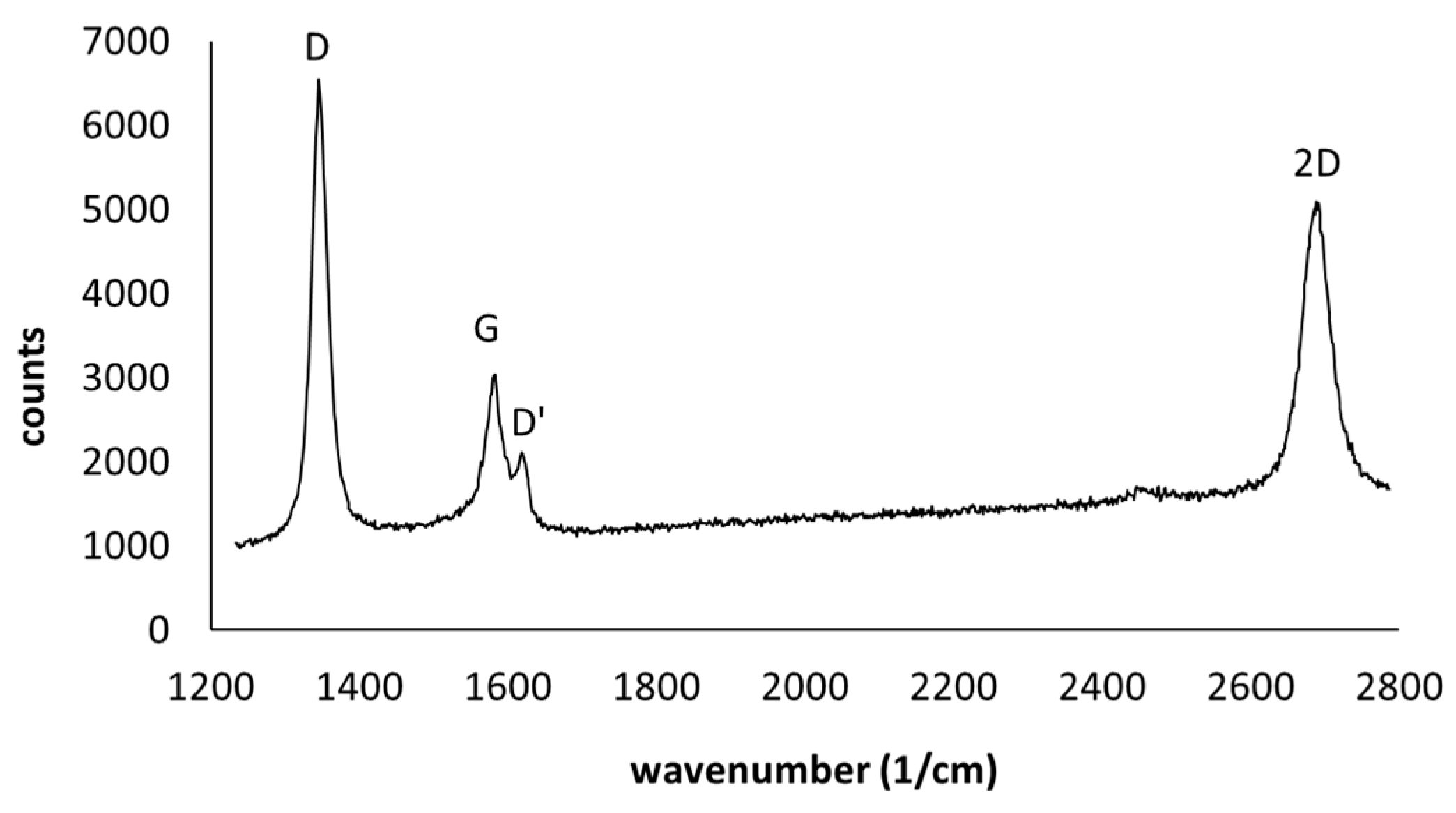
Two other lines, the D at wavenumber 1350 cm−1 and D’ at 1620 cm−1 show up after implantation. They are so called defect induced Raman modes. Example of the Raman spectrum after ion implantation is shown in Figure 2 and all four D, G, D’ and 2D lines are shown. The intensity ratio of the D and G modes I(D)/I(G) is a powerful tool for determination of the density of defects generated by ion implantation [18].
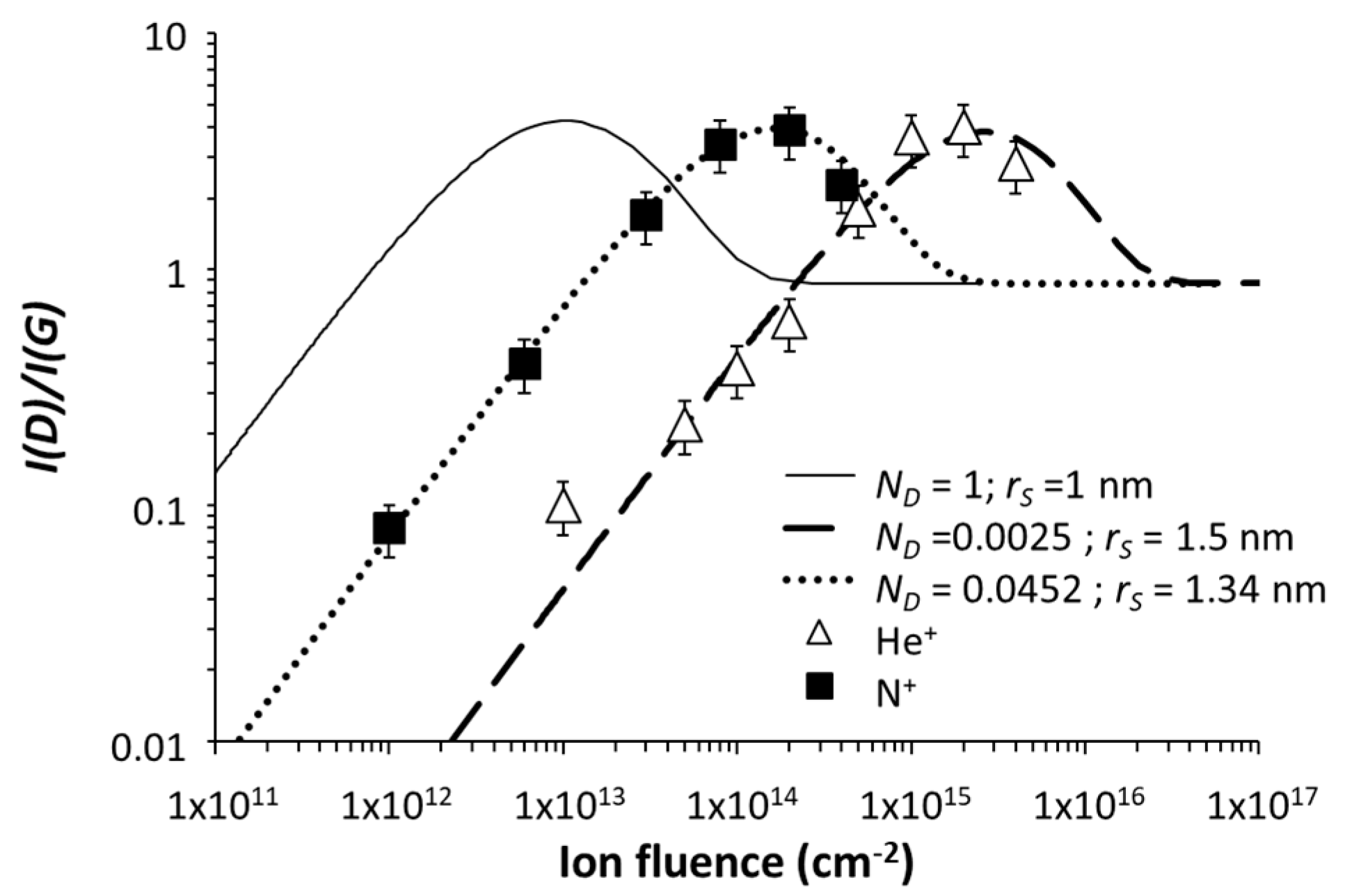
Phenomenological model proposed by Lucchese [18] predicts that the I(D)/I(G) ratio upon increase of defect density increases, reach maximum and next decreases down to some value. This model may be fitted to the experimental I(D)/I(G) ratio versus ion fluence. This fitting requires three parameters: the number of defects generated by one incident ion ND, the mean radius of ion induced defect rS, and the mean radius rA of the graphene surrounding the defect in which D mode of the Raman mode is generated. The circular area of width rA − rS surrounding the defect consists of graphene neighboring the defect boundary region and thus, is responsible for creation of the D Raman mode. The distance rA − rS = 2 nm was taken following [18] for both He+ and N+. The best fitting to the semi-empirical relation I(D)/I(G) versus ion fluence proposed in [18] with experimental data was obtained for the following fitting parameters: ND = 0.045 and ND = 0.0025 and rS = 1.34 nm and rS = 1.5 nm for N+ and He+ respectively.
The fitted curves with experimental points are shown in Figure 3. It should be noted that the mean distance between generated defects LD can be obtained directly from the defect density according to formula ND = 1/LD2.
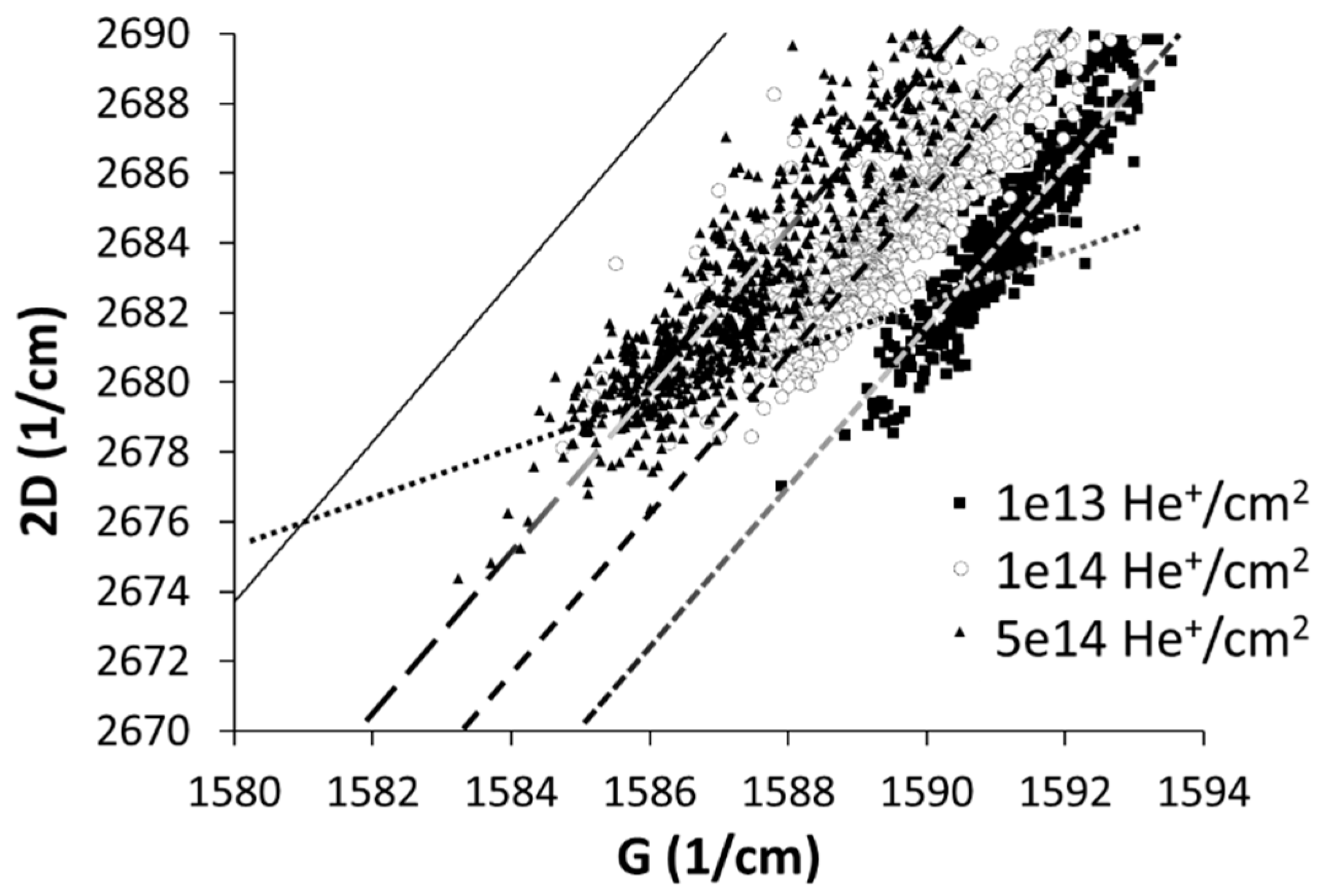
In addition to the information provided by the intensity of the D line, there are other conclusions which can be drawn from the positions of the G and 2D line. The relation between the 2D and the G line allows to evaluate the carrier concentration and strain in the graphene [19]. Such diagram of the 2D versus G line position for helium ion implantation at three different fluences is shown in Figure 4. Experimental points are arranged along parallel lines (shown in Figure 4 as broken lines) for each implantation fluence. Scatter of points along each line represents the spread of uniaxial strain existing in the graphene layer [20]. The solid line shown in Figure 4 represents the relation of 2D versus G for graphene of concentration smaller than 1 × 1012 cm−2. The drift of clouds of experimental points toward higher wave numbers of the G mode (along the dotted line) represents the increase of carrier concentration [14]. Groups of points shown in Figure 4 correspond to helium ion implantation fluences of 1 × 1013 cm−2, 1 × 1014 cm−2 and 5 × 1014 cm−2. It can be seen that with increase of implantation fluence the “clouds” of points move toward the lower wave numbers of the G mode, which indicates a decrease of carrier concentration [14].
Finally, the ratio of intensity of I(D)/I(D’) provides information about the nature of defects [21,22]. This ratio was found to be constant and close to 6–7 in the region where the D’ line was observed. This value indicates that the dominant graphene defects generated by ion implantation are vacancies.
3.2. Electrical Measurements
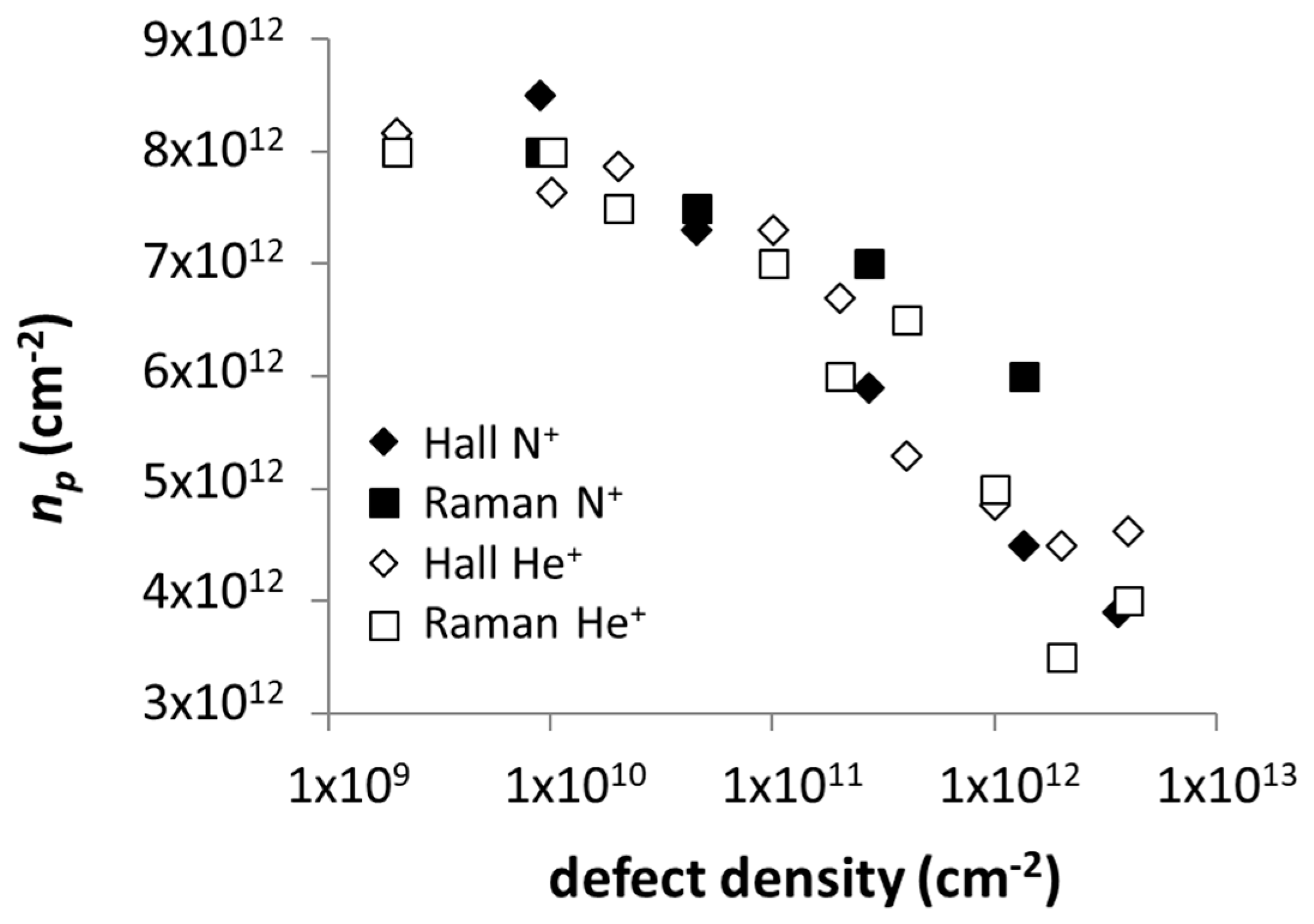
The Hall measurements have been performed after each step of ion implantation. Carrier concentration (holes) versus defect density after implantation of both helium and nitrogen ions is shown in Figure 5. It should be noted that defect density was determined from ion fluencies and ND values estimated using Raman data as was presented in Figure 3. In addition to the points obtained from electrical measurements there are also points which were determined from Raman measurements presented in Figure 5. It can be seen that there is an agreement between electrical and optical measurements for both types of ions. The carrier concentration is affected by implantation and decreases by factor of 2 for the highest defect concentration. This suggest that the decrease of hole concentration versus defect density is probably connected with defects generated inside of SiC substrate, which acts as deep donors, and therefore create traps of holes from the graphene layer.
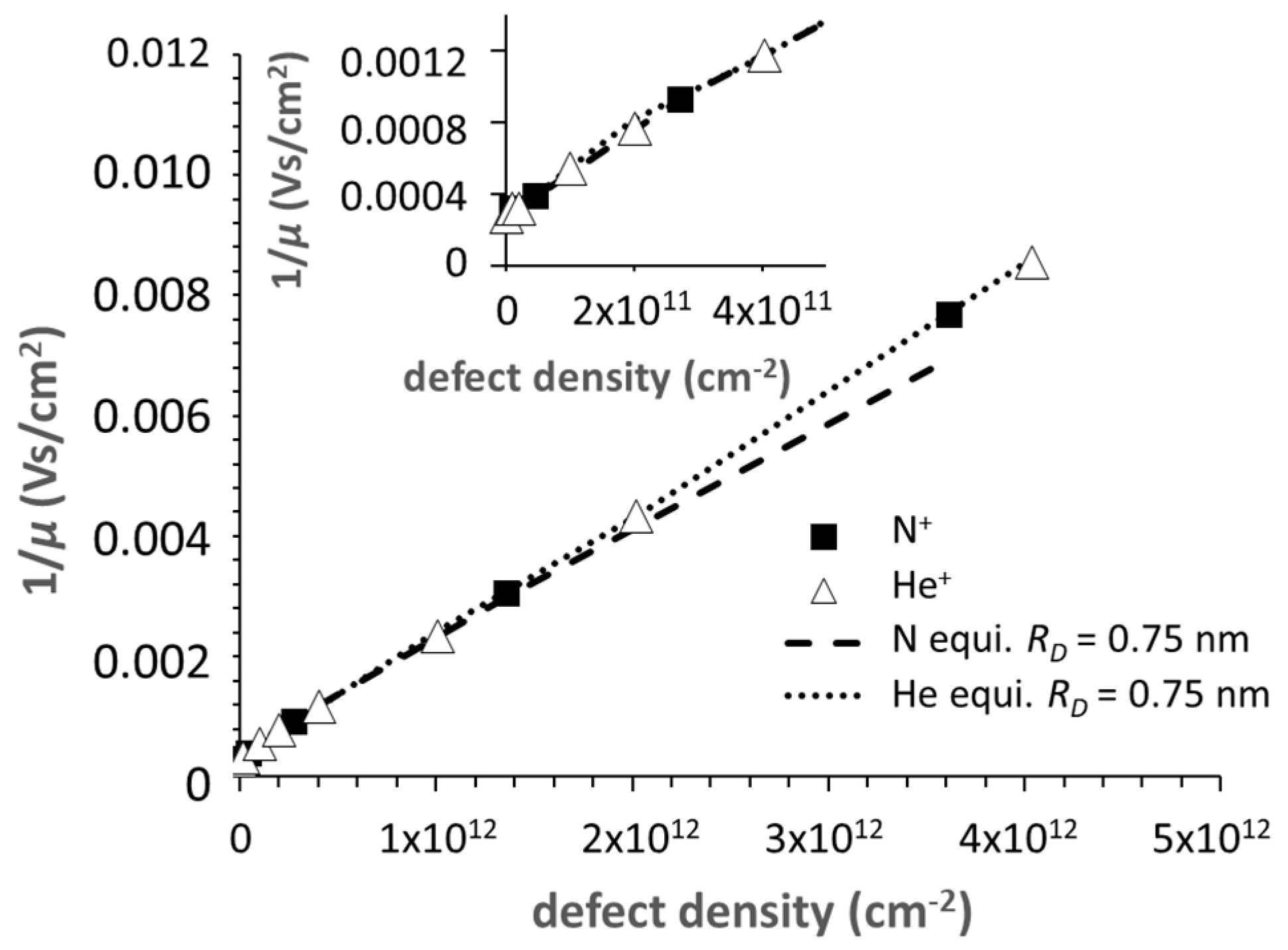
The dependence of inverse of carrier mobility versus defect density is a linear function as shown in Figure 6. This is an indication that the main scattering mechanism is connected to defects generated by ion implantation. The slope of this dependence is constant and provides information about the radius of the defect. The same slope for N+ and He+ implanted ions indicates that the carrier scattering centres created by ion implantation have the same radius RD for both ions. However, the logarithmic dependence of slope on radius of defect given in [23,24,25] assures that different defects contribute in a similar way. Equation (1) given in [23,24,25] for dependence of carrier mobility in graphene on scattering on neutral centres allows to estimate the radius of generated defects:
where µ is the mobility of holes, ND is the ion induced defect density established from the Raman measurements, n is the hole concentration determined from the electrical measurements, RD is a radius of defect which acts as a scattering centre.
1/µ = (πhND)/(2e ln2[(πn)1/2 RD])
First of all, a very good agreement with theoretical model suggests that the main scattering centre induced by ion implantation are indeed neutral centres. Defect radius RD = 0.75 nm: obtained from Hall measurements was found to be smaller than the one estimated on the basis of Raman experiments and will be discussed later on.
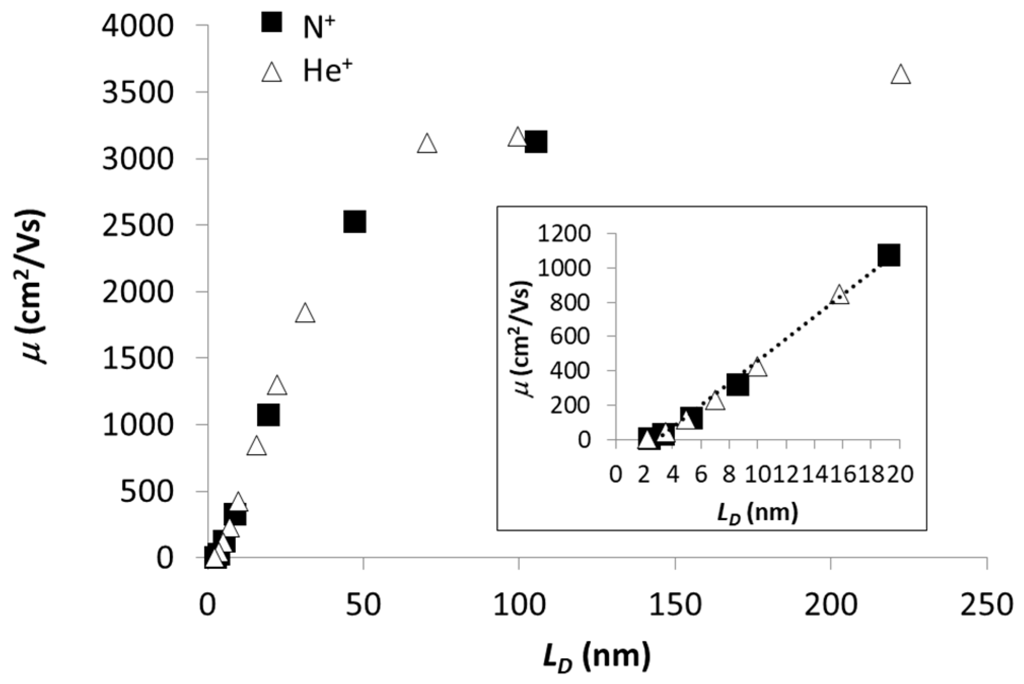
The carrier mobility versus defect distance established from defect density is shown in Figure 7. It can be seen that for well separated defects (above 50 nm) the ion implantation has a small effect on mobility value. The value of carrier mobility stays close to the initial 3000 cm2/Vs. For defect separation bellow 50 nm a strong decrease of mobility with increase of fluence of implanted He+ and N+ is observed. The mobility decreases by almost two orders of magnitude, which indicates that the main scattering mechanism is related to defects generated by ion implantation. It should be noted that there is no difference between N+ and He+ implantation which indicates that defects generated by N+ and He+ have the same nature. Moreover, a very good compliance between the effects of both applied ions suggests a correct estimation of the ion defect efficiencies for both nitrogen and helium ions determined from Raman measurements.
The region of mobility for high implanted fluences and thus for a small distance between defects shows that for LD close to 2 nm the mobility drops to zero. This is a clear indication that for distance between defects of about 2 nm a transition to hopping regime takes place. This distance is comparable to the 2rS defect size which is about 2.7–3 nm from Raman and about 2RD = 1.5 nm from Hall measurements. It means that most probably the graphene surface was covered by overlapped defects and transformed to a significant degree into amorphous carbon structures. This observation supports conclusion about a rather large size of the ion induced defects
4. Discussion and Conclusions
The probability of creating one defect by one implanted ion is relatively small. The fitting of the Raman I(D)/I(G) relation shows that this probability is 0.0025 for He+ and 0.042 for N+ ions. These small values suggest that defects have to be created by a direct collision of the falling ion with a carbon atom in the graphene lattice. This is supported by the I(D)/I(D’) ratio which is close to the value of 6–7. This value suggests that vacancy like defects play an essential role in the ion implantation process [21,22].
The Stopping and Range of Ions in Matter (SRIM) code was used for simulation of vacancy generation in the graphene lattice under the assumption that removing one carbon atom requires 21 eV [9]. The number of carbon vacancies produced by direct ion collisions are 0.00246 for He+ and 0.034 for N+. Thus, the SRIM simulations are close to the experimental results.
Therefore, it may be expected that as a result of such collisions vacancies are indeed created. The RD value established by Hall measurements at 0.75 nm is larger than the size of monovacancy. However, a missing carbon atom with three dangling bonds from graphene of lattice will not be stable. Reconstruction of the whole area may lead to a formation pentagon and polygon structure with one dangling bond. The formation energy of such defect is about 7.5–7.7 eV [26,27,28] with relatively low migration barrier of about 1.3–1.5 eV. Hence, the reconstructed monovacancy can migrate creating divacancy. Reconstructed divacancy may form one octahedron and two pentagons in the so called 5-8-5 defect without dangling bonds. Formation energy of such defect is 7.28 eV [29,30] with migration barrier about 7 eV [26]. Thus, such defect will be neutral and practically immobile. The diameter of such a defect is about 1nm, which is of the order of the defect size determined in our experiments.
Defect radius obtained from Hall measurements was about twice smaller than estimated on the basis of Raman experiments. However, it should be remembered that both methods are based on different physical phenomena and may probe different aspects of the same defect. Charge carrier mobility depends on low energy scattering associated with defect. Thus, the RD may reflect the core of the defect. The Raman measurements are based on activation of the D mode which is generated in the unaffected graphene outside of the defect in close vicinity to its limit. So, the Raman is probing the graphene area outside the defect boundary and may provide another defect size than obtained from mobility measurements. On the other hand, the distance from the defect limit at which D mode is activated rA-rS was after [18] assumed to be 2 nm. However, modification of this distance may affect the defect radius rS determined from Raman according to applied methodology [18].
The decrease of carrier mobility with the increase of defect density tends to zero for distances between defects of the order of 2 nm. This indicates that for such distances an overlap between defects takes place and leads to hopping transport. This observation supports the conclusion that the size of the ion induced defects is rather far larger than the size of a simple vacancy.
Both applied methods Hall mobility and Raman gave basically the same defect size for both applied ions of helium and nitrogen despite a big difference of their atomic masses and very different probability of the defect generation in elastic collisions. It suggests that a certain preferred configuration of the structure of the ion induced defects is created and indicates that the size of this structure is larger than mono- or divacancy.
The decrease of the carrier concentration with increasing ions fluences is probably caused by modification of the structure of SiC substrate by implantation.
We have a strong experimental evidence that our data are reflecting electrical properties of damaged graphene and not SiC implanted layer. We used semi-insulating 6H–SiC (0001), so for a low implantation range substrate does not influence the measured electrical properties. For the highest implantation fluences the electrical conductivity of graphene decreases to zero (due to mobility decreasing to zero). If implantation by He+ or N+ ions would convert damaged semi-isolated SiC to partly conductive layer it would be possible to measure a conductivity of the graphene/SiC system for the highest implantation fluence. However, this is not the case, the system of graphene/SiC does not conduct for the highest fluences of He+ or N+ implanted fluences as well. Doping of SiC by nitrogen ion implantation usually requires elevated temperature of the implanted sample during ion implantation process and subsequent annealing at high temperature as was presented in [31,32]. In our experiments, ion implantation was performed at room temperature and no annealing was applied after ion implantation. At these conditions SiC most probably was not doped by implanted nitrogen ions and did not affect electrical measurements.
In conclusion, our results proved that ion beam bombardment generates defects which act as neutral scattering centers in the graphene diminishing the carrier’s mobility. Defect sizes estimated with both experimental methods were different, however, of the same order of magnitude. The differences of defect sizes may be due to the different physical mechanism probed by the applied methods. However, the obtained defect sizes in both methods were essentially larger than for simple graphene vacancies. Thus, the most likely, defects generated in implantation process are predominantly reconstructed divacances or larger vacancy complexes.
Author Contributions
Conceptualization, P.C., G.G. and J.M.B.; methodology, P.C., G.G. and J.M.B.; validation, J.M.B., P.C. and G.G.; formal analysis, G.G., P.C. and J.M.B.; investigation, P.C. and G.G.; writing—original draft preparation, G.G., J.M.B. and P.C.; writing—review and editing, J.M.B., G.G. and P.C.
Funding
This research was funded by European Union Horizon 2020 research and innovation programme under grant agreement No. 785219 and by National Centre for Research and Development (grant PBS 3/B6/24/2015).
Acknowledgments
Sample of graphene was grown in the Department of Epitaxy and Characterization of IEMT.
Conflicts of Interest
The authors declare no conflict of interest.
References
- Ye, J.C.; Charnvanichborikarn, S.; Worslay, M.A.; Kucheyev, S.O.; Wood, B.C.; Wang, Y.M. Enhanced electrochemical performance of ion beam treated 3D graphene aerogels for lithium ion batteries. Carbon 2015, 85, 269–278. [Google Scholar] [CrossRef]
- O’Hern, S.C.; Boutillier, M.S.H.; Song, Y.; Kong, J.; Laoui, T.; Atieh, M.; Karnik, R. Selective ionic transport through tunable subnanometer pores in single-layer graphene membranes. Nano Lett. 2014, 14, 1234–1241. [Google Scholar] [CrossRef] [PubMed]
- Gawlik, G.; Ciepielewski, P.; Baranowski, J.M.; Jagielski, J. Ion beam induced defects in CVD graphene on glass. Surf. Coat. Technol. 2016, 306, 119–122. [Google Scholar] [CrossRef]
- Berger, C.; Song, Z.; Li, X.; Wu, X.; Brown, N.; Naud, C.; Mayou, D.; Li, T.; Hass, J.; Marchenkov, A.N.; et al. Electronic confinement and coherence in patterned epitaxial graphene. Science 2006, 312, 1191–1196. [Google Scholar] [CrossRef] [PubMed]
- Emtsev, K.V.; Bostwick, A.; Horn, K.; Jobst, J.; Kellogg, G.L.; Ley, L.; McChesney, J.L.; Ohta, T.; Reshanov, S.A.; Ruohrl, J.; et al. Towards wafer-size graphene layers by atmospheric pressure graphitization of silicon carbide. Nat. Mater. 2009, 8, 203–207. [Google Scholar] [CrossRef] [PubMed] [Green Version]
- Emtsev, K.V.; Seyller, T.; Speck, F.; Ley, L.; Stojanov, P.; Riley, J.D.; Leckey, R.G.C. Initial Stages of the Graphite-SiC(0001) Interface Formation Studied by Photoelectron Spectroscopy. Mater. Sci. Forum 2007, 556–557, 525–528. [Google Scholar] [CrossRef]
- Emtsev, K.V.; Speck, F.; Seyller, T.; Ley, L.; Riley, J.D. Interaction, growth, and ordering of epitaxial graphene on SiC{0001} surfaces: A comparative photoelectron spectroscopy study. Phys. Rev. 2008, 77, 155303. [Google Scholar] [CrossRef]
- Riedl, C.; Coletti, C.; Iwasaki, T.; Zakharov, A.A.; Starke, U. Quasi-Free-Standing Epitaxial Graphene on SiC Obtained by Hydrogen Intercalation. Phys. Rev. Lett. 2009, 103, 246804. [Google Scholar] [CrossRef]
- Kotakoski, J.; Brand, C.; Lilach, Y.; Cheshnovsky, O.; Mangler, C.; Arndt, M.; Meyer, J.C. Toward two-dimensional all-carbon heterostructures via ion beam pattering single layer graphene. Nano Lett. 2015, 15, 5944–5949. [Google Scholar] [CrossRef]
- Pan, C.-T.; Hinks, J.A.; Ramasse, Q.M.; Greaves, G.; Bangert, U.; Donnelly, S.E.; Haigh, S.J. In-situ observation and atomic resolution imaging of the ion irradiation induced amorphisation of graphene. Sci. Rep. 2014, 4, 6334. [Google Scholar] [CrossRef] [Green Version]
- Robertson, A.W.; Allen, C.S.; Wu, Y.A.; He, K.; Olivier, J.; Neethling, J.; Kirkland, A.I.; Warner, J.H. Spatial control of defect creation in graphene at the nanoscale. Nat. Commun. 2012, 3, 1144. [Google Scholar] [CrossRef] [PubMed] [Green Version]
- Björkman, T.; Kurasch, S.; Lehtinen, O.; Kotakoski, J.; Yazyev, O.V.; Srivastava, A.; Skakalova, V.; Smet, J.H.; Kaiser, U.; Krasheninnikov, A.V. Defects in bilayer silica and graphene: Common trends in diverse hexagonal two-dimensional systems. Sci. Rep. 2013, 3, 3482. [Google Scholar] [CrossRef] [PubMed]
- Gong, C.; Robertson, A.W.; He, K.; Lee, G.-D.; Yo, E.; Kirkland, A.I.; Warner, J.H. Thermally Induced Dynamics of Dislocations in Graphene at Atomic Resolution. ACS Nano 2015, 9, 10066–10075. [Google Scholar] [CrossRef] [PubMed]
- Das, A.; Pisana, S.; Chakraborty, B.; Piscanec, S.; Saha, S.K.; Waghmare, U.V.; Novoselov, K.S.; Krishnamurthy, H.R.; Geim, A.K.; Ferrari, A.C.; et al. Monitoring dopants by Raman scattering in an electrochemically top-gated graphene transistor. Nat. Nanotechnol. 2008, 3, 210–215. [Google Scholar] [CrossRef] [PubMed] [Green Version]
- Strupinski, W.; Grodecki, K.; Wysmolek, A.; Stepniewski, R.; Szkopek, T.; Gaskell, P.E.; Gruneis, A.; Haberer, D.; Bozek, R.; Krupka, J.; et al. Graphene Epitaxy by Chemical Vapor Deposition on SiC. Nano Lett. 2011, 11, 1786–1791. [Google Scholar] [CrossRef] [PubMed]
- Bierwagen, O.; Ive, T.; Van de Walle, C.G.; Speck, J.S. Caused of incorrect carrier-type identification in van der Pauw-Hall measurements. Appl. Phys. Lett. 2008, 93, 242108. [Google Scholar] [CrossRef]
- Ferrari, A.C.; Meyer, J.C.; Scardaci, V.; Casiraghi, C.; Lazzeri, M.; Mauri, F.; Piscanec, S.; Jiang, D.; Novoselov, K.S.; Roth, S.; et al. Raman spectrum of graphene and graphene layers. Phys. Rev. Lett. 2006, 97, 187401. [Google Scholar] [CrossRef]
- Lucchese, M.M.; Stavale, F.; Ferreira, E.H.M.; Vilani, C.; Moutinho, M.V.O.; Capaz, R.B.; Achete, C.A.; Jorio, A. Quantifying ion-induced defects and Raman relaxation length in graphene. Carbon 2010, 48, 1592–1597. [Google Scholar] [CrossRef]
- Lee, J.E.; Ahn, G.; Shim, J.; Lee, Y.S.; Ryu, S. Optical separation of mechanical strain from charge doping in graphene. Nat. Commun. 2012, 3, 1024. [Google Scholar] [CrossRef] [Green Version]
- Mohiuddin, T.M.G.; Lombardo, A.; Nair, R.R.; Bonetti, A.; Savini, G.; Jalil, R.; Bonini, N.; Basko, D.M.; Galiotis, C.; Marzari, N.; et al. Uniaxial strain in graphene by Raman spectroscopy: G peak splitting, Grüneisen parameters, and sample orientation. Phys. Rev. B 2009, 70, 205433. [Google Scholar] [CrossRef]
- Eckmann, A.; Felten, A.; Mishchenko, A.; Britelli, L.; Krupke, R.; Novoselov, K.S.; Casiraghi, C. Probing the nature of defects in graphene by Raman spectroscopy. Nano Lett. 2012, 12, 3925–3930. [Google Scholar] [CrossRef] [PubMed]
- Ochendovski, O.; Lehtinen, O.; Kaiser, U.; Turchanin, A.A.; Ban-d’Etat, B.; Lebius, H.; Karlusić, M.; Jaksić, M.; Schleberger, M. Nanostructuring graphene by dense electronic excitation. Nanotechnology 2015, 26, 465302. [Google Scholar] [Green Version]
- Chen, J.-H.; Cullen, W.G.; Jang, C.; Fuhrer, M.S.; Williams, E.D. Defect Scattering in Graphene. Phys. Rev. Lett. 2009, 102, 236805. [Google Scholar] [CrossRef] [PubMed]
- Ni, Z.H.; Ponomarenko, L.A.; Nair, R.R.; Yang, R.; Anissimova, S.; Grigorieva, I.V.; Schedin, F.; Shen, Z.X.; Hill, E.H.; Novoselov, K.S.; et al. On resonant scatterers as a factor limiting carrier mobility in graphene. Nano Lett. 2010, 10, 3868–3872. [Google Scholar] [CrossRef] [PubMed]
- Buchowicz, G.; Stone, P.R.; Robinson, J.T.; Cress, C.D.; Beeman, J.W.; Dubon, O.D. Correlation between structure and electrical transport in ion-irradiated graphene grown on Cu foils. Appl. Phys. Lett. 2011, 98, 032102. [Google Scholar] [CrossRef] [Green Version]
- El-Barbary, A.A.; Telling, R.H.; Ewels, C.P.; Heggie, M.I.; Briddon, P.R. Structure and energetics of the vacancy in graphite. Phys. Rev. B 2003, 68, 144107. [Google Scholar] [CrossRef]
- Li, L.; Reich, S.; Robertson, J. Defects energies of graphite: Density-functional calculations. Phys. Rev. B 2005, 72, 184109. [Google Scholar] [CrossRef]
- Krasheninnikov, A.V.; Lehtinen, P.O.; Foster, A.S.; Nieminen, R.M. Bending the rules: Contrasting vacancy energetics and migration in graphite and carbon nanotubes. Phys. Lett. 2006, 418, 132–136. [Google Scholar] [CrossRef]
- Lee, G.-D.; Wang, C.Z.; Yoon, E.; Hwang, N.-M.; Kim, D.-Y.; Ho, K.M. Diffusion, coalescence, and reconstraction of vacancy defects in graphene layers. Phys Rev Lett. 2005, 95, 205501. [Google Scholar] [CrossRef]
- Lee, G.-D.; Wang, C.; Yoon, E.; Hwang, N.-M.; Ho, K. Vacancy defects and formation of local haeckelite structures in graphene from tight-binding molecular dynamics. Phys. Rev. B 2006, 74, 245411. [Google Scholar] [CrossRef]
- Miyajima, T.; Tokura, N.; Fukumoto, A.; Hayashi, H.; Hara, K. Nitrogen Ion Implantation and Thermal Annealing in 6H-SiC Single Crystal. Jpn. J. Appl. Phys. 1996, 35, 1231–1234. [Google Scholar] [CrossRef]
- Gaedner, J.; Rao, M.V. Elevated temperature nitrogen implants in 6H-SiC. J. Electron. Mater. 1996, 25, 885–892. [Google Scholar] [CrossRef]
Figure 1.
The spatial map of FWHM (Full Width at Half Maximum) of the 2D Raman mode. The FWHM within 20–30 cm−1 shown by black color indicates single graphene layer.
Figure 1.
The spatial map of FWHM (Full Width at Half Maximum) of the 2D Raman mode. The FWHM within 20–30 cm−1 shown by black color indicates single graphene layer.

Figure 2.
Example of the Raman spectrum of graphene after He+ ions implantation with ion fluence 1015 cm−2.
Figure 2.
Example of the Raman spectrum of graphene after He+ ions implantation with ion fluence 1015 cm−2.

Figure 3.
Ratio of intensities of Raman lines I(D)/I(G) versus ion fluence for graphene on 6H–SiC (0001) bombarded with nitrogen ions (squares) and helium ions (triangles). Solid line represents theoretical curve of I(D)/I(G) vs. ion fluence according to [18] for ND = 1 and rS = 1 nm. Dotted and dashed lines represent theoretical dependence of I(D)/I(G) for rS = 1.34 nm and rS = 1.5 nm and ion defect efficiencies ND = 0.045 and 0.0025 for N+ and He+ respectively.

Figure 4.
The Raman 2D mode versus the G mode wave numbers for 1 × 1013 cm−2, 1 × 1014 cm−2 and 5 × 1014 cm−2 helium ion implantation fluences. The broken lines represent average of the observed ‘clouds’ of points. The solid line corresponds to slope of 2D versus G equal 2.2 resulting from pure strain [19], and the dotted line corresponds to slope 0.7 appropriate to strain free p-type graphene [19].

Figure 5.
Hole concentration np versus defect density obtained from Hall (diamonds) and from Raman measurements (squares) after nitrogen (solid points) and helium (open points) ion implantation.
Figure 5.
Hole concentration np versus defect density obtained from Hall (diamonds) and from Raman measurements (squares) after nitrogen (solid points) and helium (open points) ion implantation.

Figure 6.
Dependence of inverse of hole mobility on defect density. Black points correspond to N+ and open triangle points to He+ implanted results. Dotted line is a linear approximation of the experimental points. Dashed and dotted lines represent formula (1) with defect radius RD = 0.75 nm using Hall carrier concentration data for N+ and He+ implanted samples respectively. The offset along the y-axis shown in insert indicates the presence of other types of scatters which are not created by implantation.

Figure 7.
Hole mobility versus defect distance established from defect density. Black points correspond to N+ and open triangle points to He+. The magnified part of graph for low LD is presented in the insert.
Figure 7.
Hole mobility versus defect distance established from defect density. Black points correspond to N+ and open triangle points to He+. The magnified part of graph for low LD is presented in the insert.

© 2019 by the authors. Licensee MDPI, Basel, Switzerland. This article is an open access article distributed under the terms and conditions of the Creative Commons Attribution (CC BY) license (http://creativecommons.org/licenses/by/4.0/).
Share and Cite
MDPI and ACS Style
Gawlik, G.; Ciepielewski, P.; Baranowski, J.M. Study of Implantation Defects in CVD Graphene by Optical and Electrical Methods. Appl. Sci. 2019, 9, 544. https://doi.org/10.3390/app9030544
AMA Style
Gawlik G, Ciepielewski P, Baranowski JM. Study of Implantation Defects in CVD Graphene by Optical and Electrical Methods. Applied Sciences. 2019; 9(3):544. https://doi.org/10.3390/app9030544
Chicago/Turabian StyleGawlik, Grzegorz, Paweł Ciepielewski, and Jacek M. Baranowski. 2019. "Study of Implantation Defects in CVD Graphene by Optical and Electrical Methods" Applied Sciences 9, no. 3: 544. https://doi.org/10.3390/app9030544
Note that from the first issue of 2016, this journal uses article numbers instead of page numbers. See further details here.