Article

Scalable Production of Graphene/Semiconducting Single-Wall Carbon Nanotube Film Schottky Broadband Photodiode Array with Enhanced Photoresponse

1
State Key Laboratory of Surface Physics and Key Laboratory of Micro and Nano Photonic Structures (Ministry of Education), Department of Physics, Fudan University, Shanghai 200433, China
2
Laboratory of Advanced Materials, Fudan University, Shanghai 200433, China
3
Collaborative Innovation Center of Advanced Microstructures, Fudan University, Shanghai 200433, China
*
Authors to whom correspondence should be addressed.
Appl. Sci. 2018, 8(12), 2369; https://doi.org/10.3390/app8122369
Submission received: 24 October 2018 / Revised: 14 November 2018 / Accepted: 20 November 2018 / Published: 23 November 2018
(This article belongs to the Section Applied Physics General)

Abstract

:
A general approach was developed to fabricate graphene/semiconducting single-wall carbon nanotube (graphene/s-SWCNT) film Schottky junctions on a large scale. The graphene/s-SWCNT film photodiodes array based on the vertically stacked Schottky junction were fabricated. The all-carbon cross-shaped structure consisted of multielement graphene/s-SWCNT Schottky photodiodes and presented a rich collection of electronics and photonics. The as-fabricated carbon-based photodiode presented an ultra-broadband photodetection characteristic with a high responsivity of 1.75 A/W at near-infrared wavelengths and a fast response rise time of 15 μs. The as-fabricated device clearly showed gate-tunable and wavelength-dependent photoelectric characteristic. Moreover, the corresponding photocurrent excitation spectrum was also demonstrated. In particular, the Si compatible and high throughput fabrication process for the devices made it conducive for large-area multielement optoelectronics devices.

1. Introduction

Carbon nanomaterials, such as graphene and carbon nanotubes (CNT), are taken as the most promising candidates for next-generation materials for integrated electronic device application because of their astonishing physical properties [1,2,3,4]. However, the zero-band gap in graphene limits its application for digital electronics. Meanwhile, the single-wall carbon nanotube (SWCNT) has been investigated widely for nano integrated circuit application based on the purification technology of CNTs [3,4,5,6]. The single semiconducting SWCNT(s-SWCNT)-based devices have been especially developed for nano electronic and photonic devices [4,6], although the device manufacturing based on a single SWCNT is technically complex and not compatible with the traditional Si process, hindering their wide applications. Hence, it is important to utilize a suitable approach to maximize the advantage of carbon nanomaterials for large-scale application. Meanwhile, hybrid graphene/CNT materials show intriguing potential for widespread application [7,8,9], which offers new opportunities for optoelectronics applications. It is particularly significant for the practical preparation and development of the carbon-based optoelectronic devices, which has attracted increasing attention [9,10,11]. In a variety of devices, the metal/semiconductor Schottky photodiode—the basic key component in integrated circuits and the semiconductor industry—reveals multiple advantages, such as simple device architecture, high response speed, and high photoconductive gain [12,13,14,15,16,17]. Meanwhile, with the development of multielement detectors, high-density photodetector arrays are highly demanded. Until now, great efforts have been made to produce carbon-based photodiode, and scalable production of carbon-based Schottky photodiode arrays with well controlled architectures is still a great challenge. Recently, the high-purity SWCNT thin-film transistors have been successful fabricated [5,18] and the growth and transfer of graphene is becoming increasingly sophisticated [19,20,21], which make it feasible to construct high-quality and large-area all-carbon optoelectronic devices.
Here, we present a controllable approach for fabricating graphene/s-SWCNT film Schottky junctions and the cross-shaped film photodiode array structures based on the as-fabricated s-SWCNT/graphene Schottky junctions in a large scale. The cross-shaped structure consists of multielement graphene/s-SWCNT Schottky photodiode, which present a rich collection of electronics and photonics. The as-fabricated all-carbon Schottky photodiode was demonstrated with an ultra-broadband photodetection characteristic from ultraviolet to near infrared range with high responsivity and a fast response rise time. The gate-tunable and wavelength-dependent photoelectric characteristics of our device were also demonstrated. By virtue of the simple device architecture and the Si compatible fabrication process, the all-carbon graphene/s-SWCNT photodiode array can provide low-cost and high throughput solutions for future nano multielement optoelectronic devices.

2. Materials and Methods

The cross-shaped carbon-based structure is illustrated schematically in Figure 1a and was fabricated as follows: Firstly, the s-SWCNT dispersions was prepared using the method reported in Reference [5]. Raw arc-discharge SWCNTs were purchased from Carbon Solution Inc. (Riverside, CA, USA). Dispersants 9-(1-octylonoyl)-9H-carbazole-2,7-diyl (PCz) (Aladdin Industrial Corporation, Shanghai, China) and SWCNT (2 mg) were mixed in toluene (6 mL). The solutions were ultrasonicated with a top-tip dispergator (Sonics VC500, Newtown, Connecticut, USA) for 30 min at an amplitude level of 30% and were then centrifuged at 20,000× g for 1 h (Allegra X-22R centrifuge, Beckman China Inc., Shanghai, China) to remove the bundles and insoluble material. The supernatants were collected for characterization and fabrication of photoelectrical devices. A dip-coating method was used to fabricate the uniform s-SWCNT film on wafer-scale Si substrates with 285 nm thermal oxide. The N-doped Si substrates were purchased from Suzhou Crystal Silicon Electronic & Technology Co., Ltd. (Suzhou, China). The thickness of the SiO2 layer was allowed to fluctuate within a certain range, which did not affect the deposition of SWCNT film and the function of gate oxide in electrical characterization. The wafer-scale was immersed in SiO2/Si substrates in obtained supernatants for 6 h to form uniform s-SWCNT film. The as-fabricated s-SWCNT film was annealed at 450 °C for 15 min, which was carried out in an argon gas environment.
After the fabrication of s-SWCNT film on SiO2/Si substrates, a lithographic and oxygen plasma process was used to fabricate the s-SWCNT film pattern (Figure 1a). The corresponding real optical and SEM images of the microstructure for s-SWCNT film are shown in Figure 1a,b respectively. Next, the chemical vapor deposition (CVD)-grown graphene was transferred on top of the s-SWCNT film and a second photolithography and oxygen plasma etch was used to fabricate a graphene channel (Figure 1a). The corresponding Raman spectrum in G-band regions for as-used graphene is shown in Figure 1c, in which the intensity ratio of I2D/IG > 2.5 indicates the high crystal quality of the as-used graphene [22,23]. Finally, source-drain electrodes were deposited with Au metal contacts (100 nm) using a photolithography and electron beam evaporation process. The Cr was used to improve Au adhesion to the graphene and s-SWCNT surface. The back-gate electrode was deposited with In metal contacts (50 nm).
The SEM images were taken on a Zeiss Sigma 500 field-emission SEM system (Zeiss-China, Shanghai, China) with the acceleration voltage of 3 KV. A Renishaw RM3000 Raman microscope (laser: 514 nm with a 2 μm spot size) (Renishaw Inc., Gloucestershire, England, UK) was used to perform the Raman spectra measurement. The atomic force microscopy (AFM) (Dimension ICON, Bruker-China, Beijing, China) observations were performed in the tapping mode. For photoresponse characterization, the continuous scanning wavelength photocurrent testing platform was constructed. The light source was a high-power supercontinuum source (SC-Pro) purchased from YSL Co., Ltd. (Wuhan, China) and a monochromator was used for automatic wavelength changing (YSL Co., Ltd. Wuhan, China) The electrical measurements were carried out in a cryogenic vacuum experiment system and the data were collected by a set of circuit systems consisting of the DC power (Yokogawa 7651, Tokyo, Japan), amperemeters (Keithely 2000, Tektronix-China Inc., Shanghai, China), preamplifiers (Exclusive C7a, Pioneer Inc., Tokyo, Japan), oscilloscopes (TDs5054B, Tektronix-China Inc., Shanghai, China), and Lock in amplifiers (SRS 830, SRS Inc., Sunnyvale, CA, USA).

3. Results

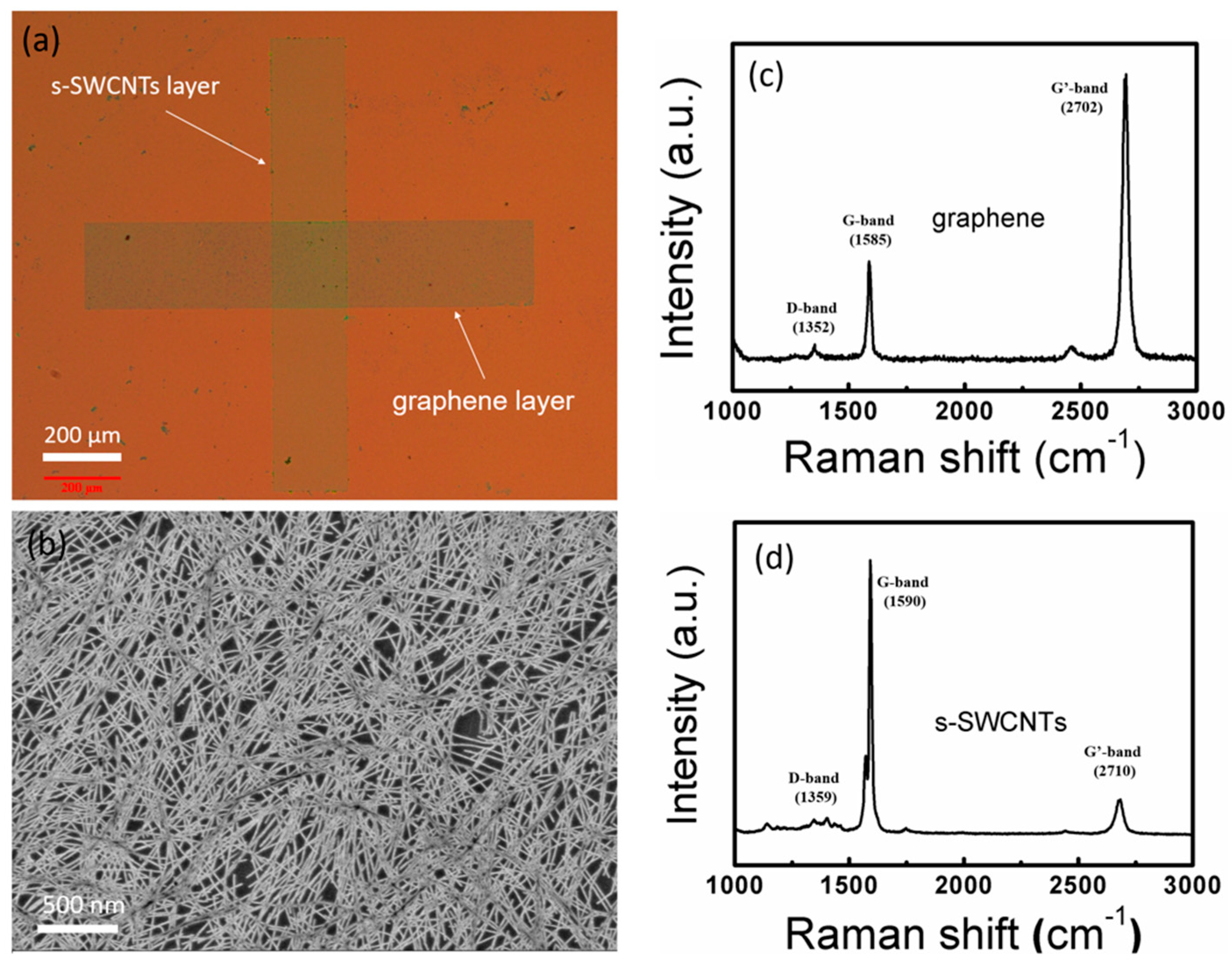
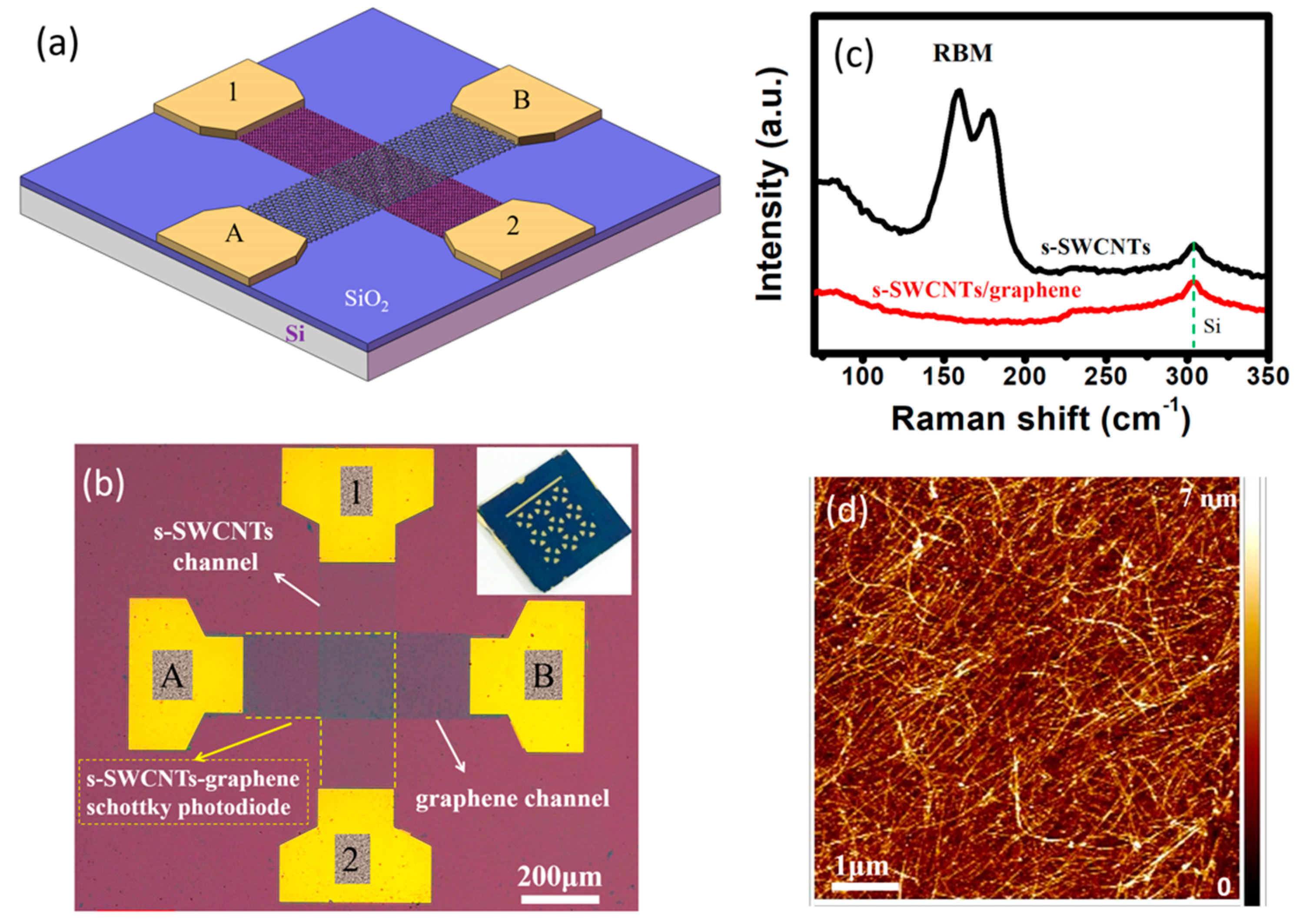
3.1. Structure and Morphology of the As-Fabricated Device

Figure 2a shows the schematic structure of the as-fabricated device, which presents a typical cross-shaped structure composed of two stacked carbon-based films, the top graphene layer, and the high-purity s-SWCNT film below. The ultraviolet-visible-near infrared (UV-Vis-NIR) absorption spectrum (Tianjin Tuo Pu Instrument Co., Ltd. Tianjin, China)and the corresponding electrical characterization of the s-SWCNTs are shown in Figure S1 in the supplementary materials, which indicates the semiconducting characteristic of the SWCNTs. The integrated semi-metallic graphene and semi-conducting s-SWCNT film were tightly stacked with uniform contrast and constructed Schottky junctions in the interface. In the process of preparation for the carbon-based devices, a dip-coating method was used to fabricate the uniform s-SWCNT film on wafer-scale Si substrates. Graphene has been used in a large-scale fabricating process by the CVD method. Based on this, our device array was expected to be fabricated in wafer scale. The Si compatible fabrication process made it conducive for large-area optoelectronic array devices. The inset in Figure 2b shows the optical image of as-fabricated graphene/s-SWCNT photodiode arrays, which cover an area of over 30 mm2, and the real optical microscope image of a single cross-shaped phototransistor structure based on the graphene/s-SWCNT Schottky junctions is shown in Figure 2b, which consists of multielement graphene/s-SWCNT photodiodes that improve the density of the phototransistor. The Raman spectrum of the as-deposited s-SWCNT film in Figure 1d presents a typical spectral characteristic for SWCNT [24,25]. From the radial breathing mode (RBM) of the Raman spectra shown in Figure 2c, we conclude the diameter of our as-deposited s-SWCNT is ~1.4 nm [25]. After stacking graphene, the RBM characteristic peak of s-SWCNT was covered up (red curve). It is speculated that the variation of the RBM Raman spectrum for graphene/s-SWCNT junctions was attributed to the unusual electron transition induced by an electrostatic doping scenario between graphene and SWCNTs. The AFM image in Figure 2d shows the surface microstructure of the graphene/s-SWCNT film overlap area, which also demonstrates the tight stacking of the two carbon layers.

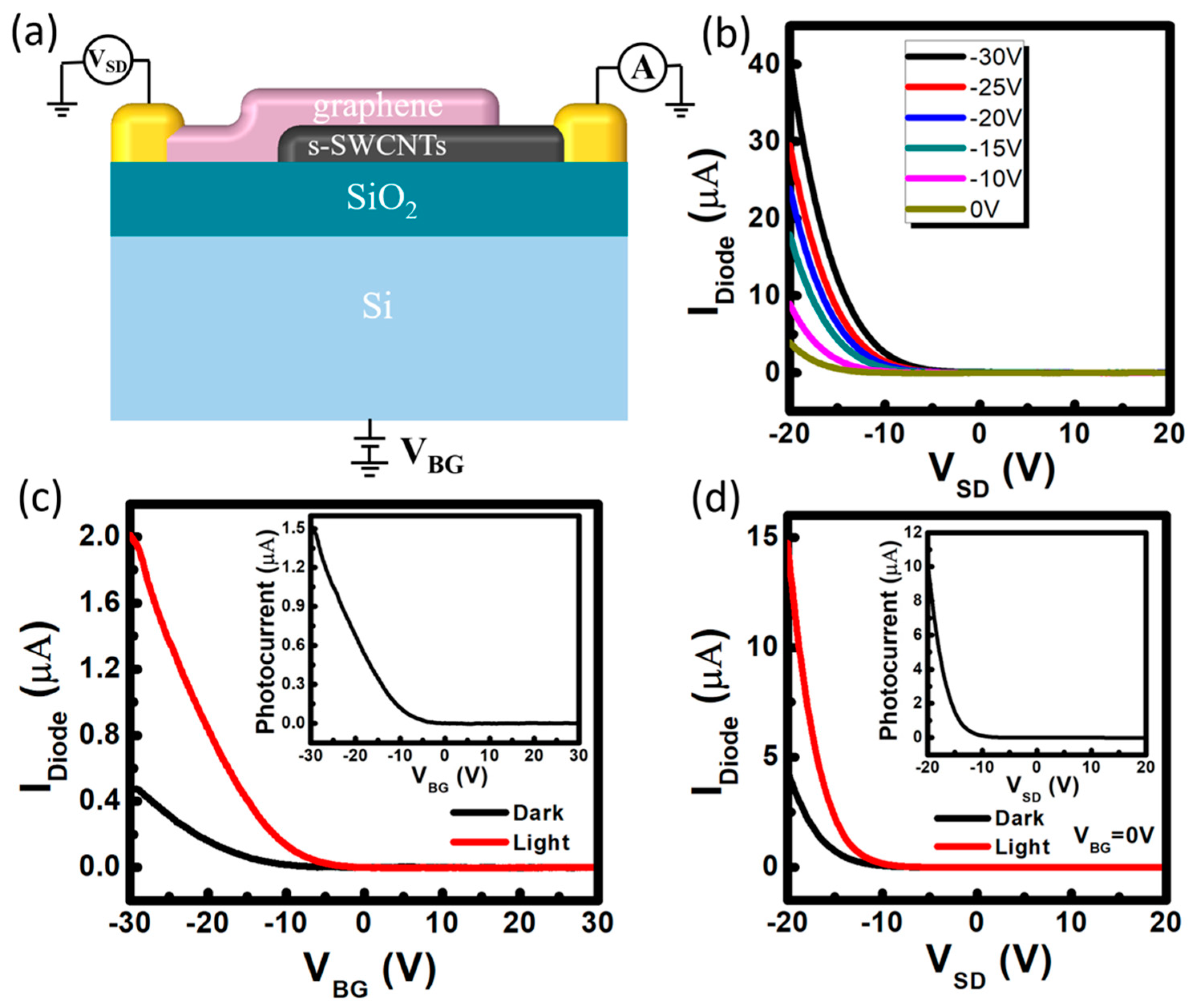
3.2. The Optoelectronic Characteristics of the Carbon-Based Photodiode

A single graphene/s-SWCNT film Schottky photodiode and the executive circuit is illustrated schematically in Figure 3a. The chemical residues created from the transfer process and the oxygen from the surrounding generally rendered a p-type graphene sheet [26]. The source-drain current of the Au–graphene–Au transistor as a function of VBG was tested, which is shown in Figure S3. An 8 V voltage of the Dirac point (VD) was observed, indicating the p-type characteristics of as-used graphene. The transfer curves of the graphene/SWCNT hybrid transistor formed by the A–B ends of the cross-shaped carbon-based structure (Figure 1 and the inset in Figure S2) were compared. We observed that the Dirac point of the hybrid transistor shifted from 8 to 15 V, indicating deeper p-type doping of the graphene/SWCNT junction. Figure 3b shows a set of output curves of the Schottky devices at different back-gate voltage (VBG) without illumination. The as-fabricated device presents a typical p-type doping characteristic ascribed to the doping effect by the surroundings and clearly exhibits a near perfect rectifying behavior. According to the electrical characteristic of SWCNTs analyzed in the supplementary materials (Figure S3a), it presents ohmic or near-ohmic contact between SWCNTs and Au electrodes [27]. In view of the fact that there is no obvious contact resistance between the graphene and Au metal, the Schottky characteristic observed in our device can be principally attributed to the graphene/SWCNT junction. By applying a reverse VBG, the diode current (IDiode) can be dramatically increased and an order of magnitude difference was observed at VBG = −30 V. The photocurrent shown in Figure 3c exhibits a continuous and monotone increasing with increasing reverse VBG (source-drain voltage (VSD) = −5 V). The back-gate tunability of the photocurrent is associated with the gate-tunable carrier density and polarity in the photoelectric conversion system. The IDiode−VSD curves of the Schottky devices at zero back-gate voltage before and after illumination is shown in Figure 3d, in which a turn-on voltage (VT) of −6.5 V was observed. Upon illumination of 1000 nm, VT was slightly decreased, which was ascribed to the enhanced image force barrier lowering (IFBL) induced by photoexcited carriers in s-SWCNTs [28,29]. This resulted in an increased diode current. Hence, the dramatically increased photocurrent with the increasing of source-drain voltage is observed in the inset of Figure 3d. The corresponding curves of the carbon-based devices in log scale are shown in Figure S2.

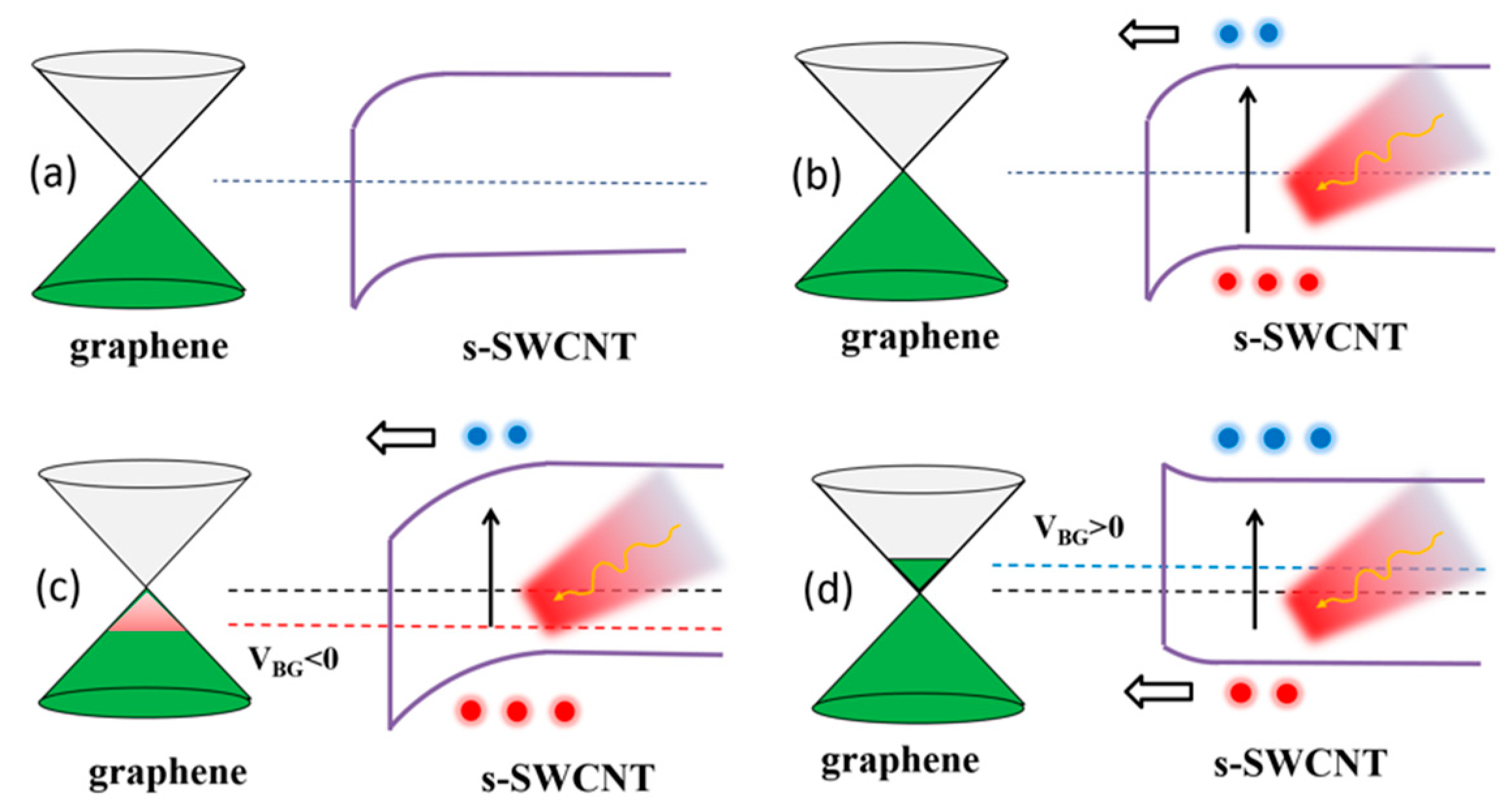
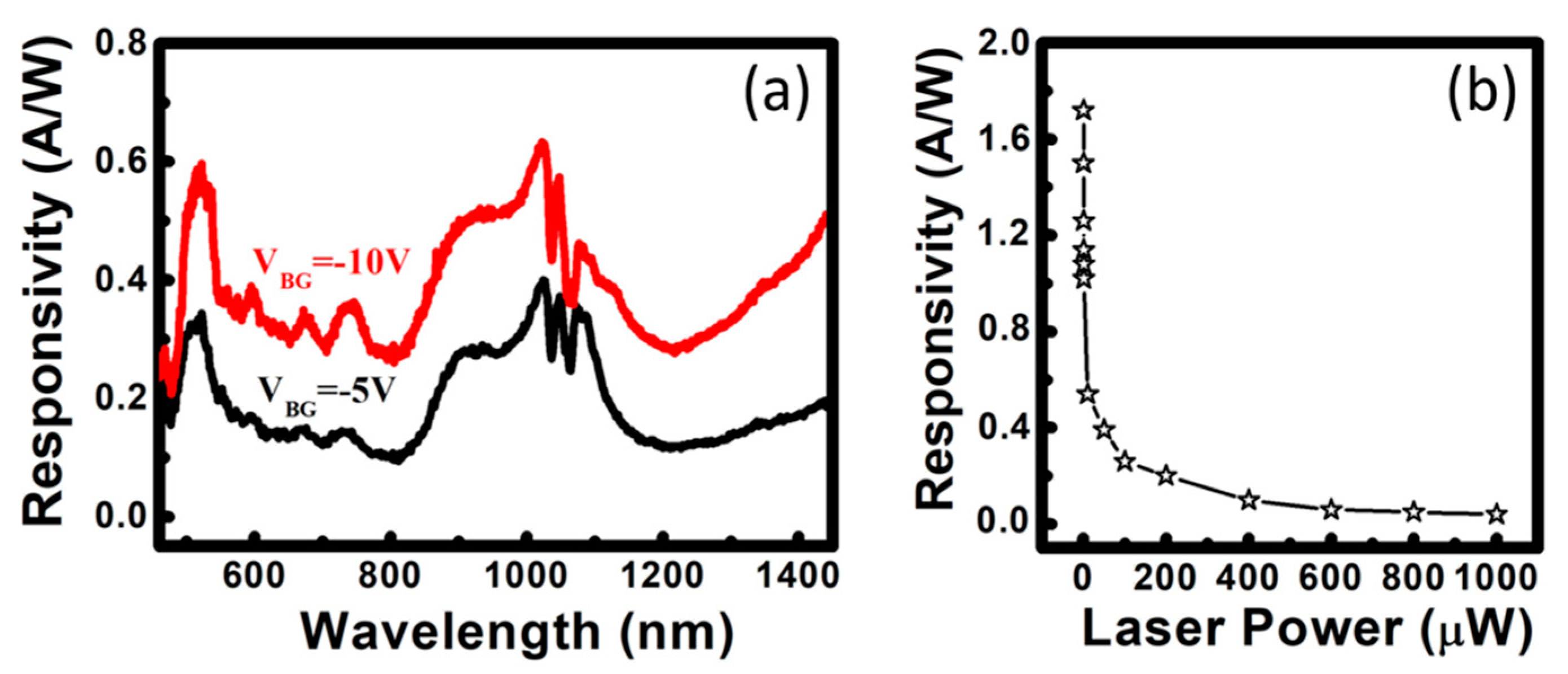
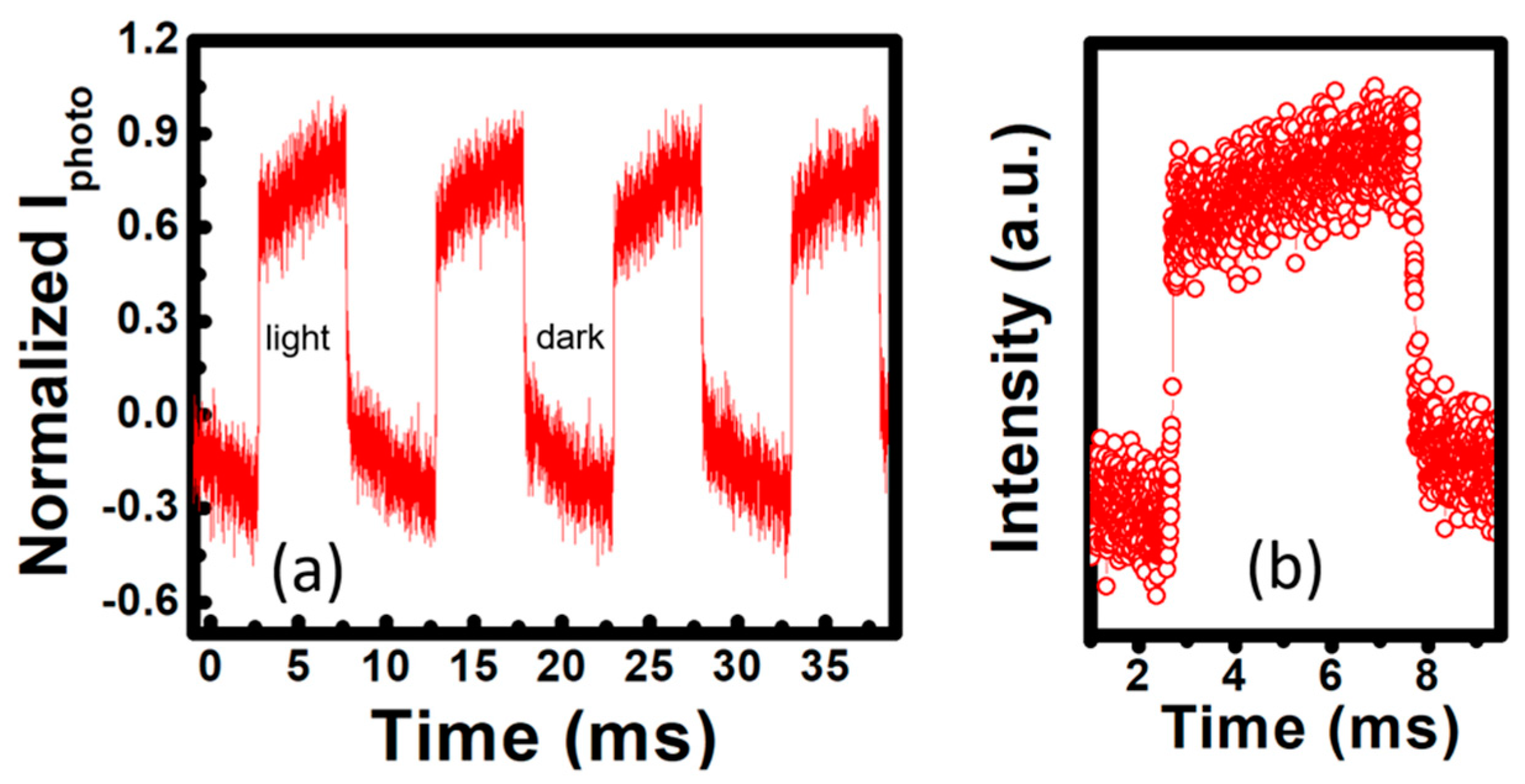
3.3. The Photodetection Characteristics and Discussion

To further verify the physical mechanisms of as-fabricated carbon-based photodiodes, the energy band diagrams at the graphene/s-SWNT junctions under various VBG are shown in Figure 4.
Since the work function of graphene is about 4.5 eV [30,31] compared with the work function of S-SWCNT, about 4.7–5.2 eV [4,32], there should be a Schottky barrier between s-SWCNTs and graphene. When graphene was transferred on the s-SWCNT film substrate, the built-in electrical field formed in graphene/s-SWCNT Schottky interface (Figure 4a). As shown in Figure 4b, at zero gate-bias under illumination, ground-state electrons of SWNTs were excited into excited states. Then, electron-hole pairs generated in the s-SWCNT film and photoexcited electrons transported from s-SWNTs to graphene under the built-in field at the SWNT–graphene junction. There were existing traps acted as carrier capture centers in SWCNT film [7,33] and some photo-generated holes were trapped with long lifetimes in the capture centers of s-SWNTs, which made the photogenerated electrons recycle several times in the circuit before they were recombined, yielding a photoconductive gain. The tunable charge carriers’ transport characteristics with VBG was also demonstrated. When VBG < 0, the lowered Fermi level of graphene resulted in a steeper upward band bending (Figure 4c) and an enhanced built-in electric field at the s-SWNT–graphene Schottky junction, while the effective Schottky barrier height was increased. More photoelectrons transferred from s-SWNTs to graphene and contributed to an increasing photocurrent. When VBG > 0, the Fermi level of graphene was raised up, resulting in the reduced effective Schottky barrier height and weakened built-in electric field, so there were few photogenerated carriers contributing to the photocurrent (Figure 4d). Meanwhile, there was no diode current observed when VBG > 0, which is consistent with the p-type electric conductivity of the carbon-based device.
For photodiodes, responsivity is a key figure of merit for the performance. In our carbon-based Schottky device, the responsivity can be described by the following equation [34,35,36]:
R = I p h o t o P = e P h υ η G 1 P = e h υ η G .
Here, h is Planck’s constant, ν is the excitation light frequency, η is the efficiency factor depended on the absorption efficiency and charge transfer efficiency in the as-fabricated graphene/s-SWCNTs Schottky junction, and G is the photoconductive gain.
Firstly, to investigate the photoresponse characteristics of our device, the responsivity-wavelength excitation spectrum was generated and is shown in Figure 5a, where the device exhibits ultra-broadband photoresponse characteristics from ultraviolet to near infrared wavelengths (VSD = −5 V, VBG ~ −5 V). The photoelectric testing was performed under the 0.1 mW irradiation at a temperature of 100 K to suppress the outside interference. The wavelength-dependent photoresponse was consistent with the absorption spectrum of the graphene/s-SWNT hybrid film. With a high reverse VBG of −10 V, the responsivity presented a significant increase over the broad excitation spectrum range, which is consistent with the diode characteristics described in Figure 3. From the equation above, the value of responsivity is proportional to photoconductive gain, which depends on the carriers’ lifetime, mobility, and source-drain bias voltage setting on the device [19]. In our carbon-based photodiode, the high trapped holes lifetime and ultra-high mobility in the graphene channel co-contributed to the high photoconductive gain and a high responsivity. Figure 5b plots the responsivity curve as a function of illumination power under the excitation wavelength of 1000 nm (VSD = −5 V, VBG = −5 V). The responsivity decreased exponentially with increasing power. This may correlate to the decrease of unoccupied states in the conduction bands of graphene and s-SWCNTs as the power increases [35]. At a 0.5 μW illumination, the device exhibited a drastically enhanced responsivity of 1.75 A/W, as compared with a single CNT-based or bare graphene-based device of 101–103 μA/W [10,37,38], which could be further improved by shrinking the size of devices and optimizing fabricating technology.
Response time is another key quality factor for photodiodes. Figure 6a shows the time trace of the photocurrent for our devices under periodic illumination (1000 nm wavelength, 100 μW, VSD = −5 V, and VBG = −10 V). All the fabricated devices were arrayed in a wafer substrate (there were nine devices in a transistors array, the inset of Figure 2b), which present a uniform and stable performance. The single carbon-based device tested the time trace of the photocurrent under periodic illumination of 5ms (Figure 6a), and after longstanding on–off cycles of one hour the photocurrent exhibited excellent reproducibility. The high-resolution temporal response of the device is shown in Figure 6b and a significant temporal photoresponse was observed in which we estimated the rise response time to be 15 μs, 7 times faster than a hybrid graphene/CNT photodetector based on photogating effect [7]. The high-quality graphene and s-SWCNT together with the effective Schottky junctions in the interface, which resulted in fast transfer of photocarriers within the s-SWNT/graphene junction, co-contributed to the excellent temporal photoresponse. When the light was off, the trapped carriers in s-SWCNT film released slowly from different surface states, which led to a slow decay of the temporal photoresponse (Figure 6b).

4. Conclusions

In summary, a general approach was developed to fabricate graphene/s-SWCNT film Schottky junctions in a large scale. The all-carbon high-performance photodiodes array based on graphene/s-SWCNT film Schottky junctions were fabricated, which exhibited enhanced photodetection capabilities at a broad excitation wavelength range. The fabricated all-carbon devices clearly showed gate-tunable photoelectric characteristic, where the magnitude of the photocurrent was increased by back-gate bias voltages. The wavelength-dependent photodetection characteristic and the corresponding photocurrent excitation spectrum was also demonstrated. Benefiting from the ultra-fast response time, large-scale fabrication process, and high-density diode array, the devices exhibited great potential applications for nano integrated electronic devices and as multielement detectors.

Supplementary Materials

The following are available online at https://www.mdpi.com/2076-3417/8/12/2369/s1. Figure S1: The semiconducting characteristic of the SWCNTs.; Figure S2: The electrical characteristic curves of the carbon-based devices in log scale. Figure S3: The contact resistance effects in Carbon-based thin film transistors.

Author Contributions

J.C. conceived and performed the experiments, analyzed the data, and wrote the paper. Z.A. provided the experimental materials and laboratory equipment and directed the research. Y.Z., X.G., and R.Q. contributed to the discussion and interpretation of the results.

Funding

This work was supported by National Key Research Program of China under Grant No. 2016YFA0302000, National Natural Science Foundation of China (Grant Nos. 11674070/11634012/11427807) and Shanghai Science and Technology Committee under Grant No. 18JC1410300/16JC1400400.

Acknowledgments

Part of the experimental work was carried out at the Fudan Nanofabrication Laboratory.

Conflicts of Interest

The authors declare no conflicts of interest.

References

  1. Lin, Y.M.; Valdes-Garcia, A.; Han, S.J.; Farmer, D.B.; Meric, I.; Sun, Y.; Wu, Y.; Dimitrakopoulos, C.; Grill, A.; Avouris, P.; et al. Wafer-scale graphene integrated circuit. Science 2011, 332, 1294–1297. [Google Scholar] [CrossRef] [PubMed]
  2. Geim, A.K. Graphene: Status and prospects. Science 2009, 324, 1530–1534. [Google Scholar] [CrossRef] [PubMed]
  3. Baughman, R.H.; Zakhidov, A.A.; De Heer, W.A. Carbon nanotubes—The route toward applications. Science 2002, 297, 787–792. [Google Scholar] [CrossRef] [PubMed]
  4. McEuen, P.L.; Fuhrer, M.S.; Park, H. Single-walled carbon nanotube electronics. IEEE Trans. Nanotechnol. 2002, 99, 78–85. [Google Scholar] [CrossRef]
  5. Gu, J.; Han, J.; Liu, D.; Yu, X.; Kang, L.; Qiu, S.; Jin, H.H.; Li, H.B.; Li, Q.W.; Zhang, J. Solution-Processable High-Purity Semiconducting SWCNTs for Large-Area Fabrication of High-Performance Thin-Film Transistors. Small 2016, 12, 4993–4999. [Google Scholar] [CrossRef] [PubMed]
  6. Martel, R.; Derycke, V.; Lavoie, C.; Appenzeller, J.; Chan, K.K.; Tersoff, J.; Avouris, P. Ambipolar electrical transport in semiconducting single-wall carbon nanotubes. Phys. Rev. Lett. 2001, 87, 256805. [Google Scholar] [CrossRef] [PubMed]
  7. Liu, Y.; Wang, F.; Wang, X.; Wang, X.; Flahaut, E.; Liu, X.; Li, Y.; Wang, X.; Xu, Y.; Shi, Y.; et al. Planar carbon nanotube–graphene hybrid films for high-performance broadband photodetectors. Nat. Commun. 2015, 6, 8589. [Google Scholar] [CrossRef] [PubMed] [Green Version]
  8. Tung, V.C.; Chen, L.M.; Allen, M.J.; Wassei, J.K.; Nelson, K.; Kaner, R.B.; Yang, Y. Low-temperature solution processing of graphene−carbon nanotube hybrid materials for high-performance transparent conductors. Nano Lett. 2009, 9, 1949–1955. [Google Scholar] [CrossRef] [PubMed]
  9. Sun, H.; You, X.; Deng, J.; Chen, X.; Yang, Z.; Ren, J.; Peng, H. Novel graphene/carbon nanotube composite fibers for efficient wire-shaped miniature energy devices. Adv. Mater. 2014, 26, 2868–2873. [Google Scholar] [CrossRef] [PubMed]
  10. Xia, F.; Mueller, T.; Lin, Y.M.; Valdes-Garcia, A.; Avouris, P. Ultrafast graphene photodetector. Nat. Nanotechnol. 2009, 4, 839. [Google Scholar] [CrossRef] [PubMed]
  11. Zubair, A.; Wang, X.; Mirri, F.; Tsentalovich, D.E.; Fujimura, N.; Suzuki, D.; Soundarapandian, K.P.; Kawano, Y.; Pasquali, M.; Kono, J. Carbon nanotube woven textile photodetector. Phys. Rev. Mater. 2018, 2, 015201. [Google Scholar] [CrossRef] [Green Version]
  12. Lee, S.; Lee, Y.; Young Kim, D.; Song, E.B.; Min Kim, S. Back-gate tuning of Schottky barrier height in graphene/zinc-oxide photodiodes. Appl. Phys. Lett. 2013, 102, 242114. [Google Scholar] [CrossRef]
  13. Liang, S.; Sheng, H.; Liu, Y.; Huo, Z.; Lu, Y.; Shen, H. ZnO Schottky ultraviolet photodetectors. J. Cryst. Growth 2011, 225, 110–113. [Google Scholar] [CrossRef]
  14. Sciuto, A.; Mazzillo, M.C.; Di Franco, S.; Mannino, G.; Badalà, P.; Renna, L.; Caruso, C. UV-A sensor based on 6H-SiC Schottky photodiode. IEEE Photonics J. 2017, 9, 1–10. [Google Scholar] [CrossRef]
  15. Di Bartolomeo, A.; Luongo, G.; Giubileo, F.; Funicello, N.; Niu, G.; Schroeder, T.; Lisker, M.; Lupina, G. Hybrid graphene/silicon Schottky photodiode with intrinsic gating effect. 2D Mater. 2017, 4, 025075. [Google Scholar] [CrossRef] [Green Version]
  16. Yang, J.; Guo, L.; Guo, Y.; Hu, W.; Zhang, Z. Epitaxial graphene/SiC Schottky ultraviolet photodiode with orders of magnitude adjustability in responsivity and response speed. Appl. Phys. Lett. 2018, 112, 103501. [Google Scholar] [CrossRef]
  17. Di Bartolomeo, A.; Grillo, A.; Urban, F.; Iemmo, L.; Giubileo, F.; Luongo, G.; Amato, G.; Croin, L.; Sun, L.; Liang, S.-J.; et al. Asymmetric Schottky Contacts in Bilayer MoS2 Field Effect Transistors. Adv. Funct. Mater. 2018, 28, 1800657. [Google Scholar] [CrossRef]
  18. Li, Z.; Ding, J.; Lefebvre, J.; Malenfant, P.R. Surface effects on network formation of conjugated polymer wrapped semiconducting single walled carbon nanotubes and thin film transistor performance. Org. Electron. 2015, 26, 15–19. [Google Scholar] [CrossRef]
  19. Deokar, G.; Avila, J.; Razado-Colambo, I.; Codron, J.-L.; Boyaval, C.; Galopin, E.; Asensio, M.-C.; Vignaud, D. Towards high quality CVD graphene growth and transfer. Carbon 2015, 89, 82–92. [Google Scholar] [CrossRef]
  20. Wang, H.; Yu, G. Direct CVD Graphene Growth on Semiconductors and Dielectrics for Transfer-Free Device Fabrication. Adv. Mater. 2016, 28, 4956–4975. [Google Scholar] [CrossRef] [PubMed]
  21. Gao, L.; Ni, G.X.; Liu, Y.; Liu, B.; Neto, A.H.C.; Loh, K.P. Face-to-face transfer of wafer-scale graphene films. Nature 2014, 505, 190. [Google Scholar] [CrossRef] [PubMed]
  22. Dresselhaus, M.S.; Jorio, A.; Hofmann, M.; Dresselhaus, G.; Saito, R. Perspectives on carbon nanotubes and graphene Raman spectroscopy. Nano Lett. 2010, 10, 751–758. [Google Scholar] [CrossRef] [PubMed]
  23. Malard, L.M.; Pimenta, M.A.A.; Dresselhaus, G.; Dresselhaus, M.S. Raman spectroscopy in graphene. Phys. Rep. 2009, 473, 51–87. [Google Scholar] [CrossRef]
  24. Kataura, H.; Kumazawa, Y.; Maniwa, Y.; Umezu, I.; Suzuki, S.; Ohtsuka, Y.; Achiba, Y. Optical properties of single-wall carbon nanotubes. Synth. Met. 1999, 103, 2555–2558. [Google Scholar] [CrossRef]
  25. Alvarez, L.; Righi, A.; Guillard, T.; Rols, S.; Anglaret, E.; Laplaze, D.; Sauvajol, J.L. Resonant Raman study of the structure and electronic properties of single-wall carbon nanotubes. Chem. Phys. Lett. 2000, 316, 186–190. [Google Scholar] [CrossRef]
  26. Pirkle, A.; Chan, J.; Venugopal, A.; Hinojos, D.; Magnuson, C.W.; McDonnell, S.; Colombo, L.; Vogel, E.M.; Ruoff, R.S.; Wallace, R.M. The effect of chemical residues on the physical and electrical properties of chemical vapor deposited graphene transferred to SiO2. Appl. Phys. Lett. 2011, 99, 122108. [Google Scholar] [CrossRef]
  27. Xia, J.Y.; Dong, G.D.; Tian, B.Y.; Yan, Q.P.; Han, J.; Qiu, S.; Li, Q.-W.; Liang, X.-L.; Peng, L.-M. Contact resistance effects in carbon nanotube thin film transistors. Acta Phys.-Chem. Sin. 2016, 32, 1029–1035. [Google Scholar] [CrossRef]
  28. Zeng, L.; Xia, Z.; Du, G.; Kang, J.; Han, R.Q.; Liu, X. Gate-induced image force barrier lowering in Schottky barrier FETs. IEEE Trans. Nanotechnol. 2009, 8, 10–15. [Google Scholar] [CrossRef]
  29. Rideout, V.L.; Crowell, C.R. Effects of image force and tunneling on current transport in metal-semiconductor (Schottky barrier) contacts. Solid-State Electron. 1970, 13, 993–1009. [Google Scholar] [CrossRef]
  30. Yu, Y.J.; Zhao, Y.; Ryu, S.; Brus, L.E.; Kim, K.S.; Kim, P. Tuning the graphene work function by electric field effect. Nano Lett. 2009, 9, 3430–3434. [Google Scholar] [CrossRef] [PubMed]
  31. Filleter, T.; Emtsev, K.V.; Seyller, T.; Bennewitz, R. Local work function measurements of epitaxial graphene. Appl. Phys. Lett. 2008, 93, 133117. [Google Scholar] [CrossRef]
  32. Liu, P.; Sun, Q.; Zhu, F.; Liu, K.; Jiang, K.; Liu, L.; Li, Q.; Fan, S. Measuring the work function of carbon nanotubes with thermionic method. Nano Lett. 2008, 8, 647–651. [Google Scholar] [CrossRef] [PubMed]
  33. Konstantatos, G.; Badioli, M.; Gaudreau, L.; Osmond, J.; Bernechea, M.; De Arquer, F.P.G.; Gatti, F.; Koppens, F.H.L. Hybrid graphene–quantum dot phototransistors with ultrahigh gain. Nat. Nanotechnol. 2012, 7, 363. [Google Scholar] [CrossRef] [PubMed]
  34. Liao, Z.M.; Lu, Y.; Xu, J.; Zhang, J.M.; Yu, D.P. Temperature dependence of photoconductivity and persistent photoconductivity of single ZnO nanowires. Appl. Phys. A 2009, 95, 363–366. [Google Scholar] [CrossRef]
  35. Fang, H.; Hu, W. Photogating in low dimensional photodetectors. Adv. Sci. 2017, 4, 1700323. [Google Scholar] [CrossRef] [PubMed]
  36. Beck, W.A. Photoconductive gain and generation-recombination noise in multiple-quantum-well infrared detectors. Appl. Phys. Lett. 1993, 63, 3589–3591. [Google Scholar] [CrossRef]
  37. Gabor, N.M.; Zhong, Z.; Bosnick, K.; Park, J.; McEuen, P.L. Extremely efficient multiple electron-hole pair generation in carbon nanotube photodiodes. Science 2009, 325, 1367–1371. [Google Scholar] [CrossRef] [PubMed]
  38. Xia, F.N.; Mueller, T.; Golizadeh-Mojarad, R.; Freitag, M.; Lin, Y.M.; Tsang, J.; Perebeinos, V.; Avouris, P. Photocurrent Imaging and Efficient Photon Detection in a Graphene Transistor. Nano Lett. 2009, 9, 1039–1044. [Google Scholar] [CrossRef] [PubMed] [Green Version]
Figure 1. (a) The optical image of the graphene/semiconducting single-wall carbon nanotube (graphene/s-SWCNT) cross-shaped films. (b) The SEM image of the as-deposited s-SWCNT film (c) The Raman spectrum in G-band regions for the chemical vapor deposition (CVD)-grown graphene after it was transferred on the top of s-SWCNT film. (d) The Raman spectrum in G-band regions for as-deposited s-SWCNT film.
Applsci 08 02369 g001
Figure 2. Schematic (a) and optical image (b) of the graphene/s-SWCNTs cross-shaped photodiode. (c) The radial breathing mode (RBM) range of Raman spectrum for the s-SWCNT film before and after overlapping graphene. (d) The AFM image of the graphene/s-SWCNT film overlap area.
Applsci 08 02369 g002
Figure 3. (a) Schematic of the graphene/s-SWCNT Schottky photodiode and the test perform circuit. (b) The output characteristics curve of the as-fabricated diode at different VBG. (c) The diode current as a function of back-gate bias for the Schottky device before and after under illumination (VSD = −5 V). The insert is the corresponding Iphoto−VBG curves. (d) The VSD-dependent diode current with and without illumination. The insert is the corresponding Iphoto−VSD curve.
Applsci 08 02369 g003
Figure 4. The energy level diagram at the graphene/s-SWCNT junction under different bias and illumination condition. (a) VSD = 0, VBG = 0, dark (b) VSD < 0, VBG = 0, light (c) VSD < 0, VBG < 0, light (d) VSD < 0, VBG > 0, light.
Applsci 08 02369 g004
Figure 5. (a) Responsivity as a function of excitation wavelength for as-fabricated carbon-based photodiode. (b) The dependence of responsivity on excitation power under the 1000 nm illumination.
Applsci 08 02369 g005
Figure 6. (a) The time trace of the photocurrent under periodic illumination. (b) The temporal photoresponse of as-fabricated device.
Applsci 08 02369 g006

