
Optimal Design Analysis with Simulation and Experimental Performance Investigation of High-Power Density Telecom PFC Converters


Electrical & Electronics and Communication Engineering Department, Koreatech University, Cheonan-si 31253, Korea
*
Author to whom correspondence should be addressed.
Appl. Sci. 2021, 11(17), 7911; https://doi.org/10.3390/app11177911
Submission received: 27 July 2021
/
Revised: 20 August 2021
/
Accepted: 25 August 2021
/
Published: 27 August 2021
(This article belongs to the Special Issue Design and Analysis of Electrical Machines and Drives)
Abstract
:The spread of the 5G technology in the telecom power applications increased the need to supply high power density with higher efficiency and higher power factor. Thus, in this paper, the performance of the different power factor correction ( PFC ) topologies implemented to work with high power density telecom power applications are investigated. Two topologies, namely the conventional and the bridge interleaved continues-current-conduction mode (CCM) PFC boost converters are designed. Selection methodology of the switching elements, the manufacturing of the boost inductors, and the optimal design for the voltage and current control circuits based on the proposed small signal stability modeling are presented. The printed circuit board (PCB) for the two different PFC topologies with a power rating of 2 kW were designed. PSIM simulation and the experiments are used to show the supply current total harmonic distortions (THD), voltage ripples, power efficiency, and the power factor for the different topologies with different loading conditions.
1. Introduction
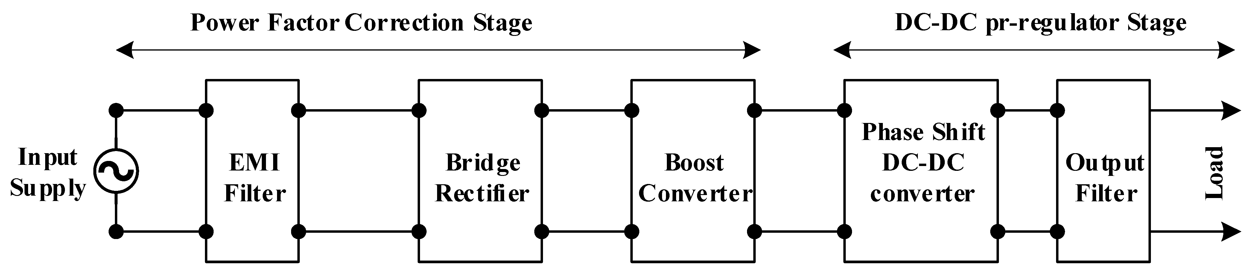
Many of the industrial applications including telecom power applications currently used active-controlled AC/DC converters to offer efficient power supplies with high-power density. Most of the active-controlled AC/DC converters are designed based on the boost converter technique, optimal design, and controlling of the operation of the boost converter at high power density offers high input power factor (PF), reducing total harmonic distortion (THD) and the circuit power losses, and increasing the conversion efficiency [1,2]. The AC/DC power supply with two stages, as illustrated in Figure 1, is the optimal configuration to obtain high values for the input PF and power efficiency. Two-stage active AC/DC telecom power supply consists of the PFC (power factor correction ) to regulate the input power factor and the DC/DC converter stage, which is used to regulate the bus voltage of the PFC stage (320–410 V) to the telecom power applications voltage level (45–63 V) [3,4].
The front stage of the telecom AC-DC power supply is the PFC stage which implements to deliver the power conversion with lower reactive power consumption, lower total harmonic distortion (THD), and, then, input supply power with a high-power factor (PF).
According to the power applications, many types of PFC converters are widely used, such as the conventional [5,6,7], the interleaved [8,9,10,11], and bridgeless [12,13,14] PFC boost converters. The conventional PFC topology as shown in Figure 2a is the basic topology as most the other PFC converters are derived from this topology. Moreover, for most of the power applications, this circuit topology is the most commonly used circuit because of its good performance, low cost, simple operations, and lower requirements for the power and control circuit designs, but the electromagnetic interface (EMI) level of the conventional CCM (continues-current-conduction mode ) PFC is high due to the high ripple current in the input side [1,15].
Another technique to implement the PFC converters can be classified as interleaved PFC boost converters as shown in the schematic circuit in Figure 2b. Interleaving means channeling the power flow from the input to the output into two or more channels and add them at the output point. By doing this, the problem of the input ripple current can be solved, also, as the number of interleaved channels increased, the power rating will be increased. Another advantage of this approach is better thermal performance as it uses two inductors which are approximately half the size of the conventional topology. The use of two inductors with a small current rating reduces the total size and total weight of the boost inductor, furthermore, it can increase the thermal performance of the converter.
Recently, different emerging techniques to improve the performance of the interleaved PFC converters are employed such as; the modification on the interleaved PFC circuit by connecting series capacitor to reduce the switching losses, reduced the voltage stress across the semiconductors as compared with the traditional interleaved boost converter [16], also, the proposed technology to minimize the input current ripple of the interleaved PFC converter by controlling the switching driving signals and without any change in the converter model parameter, which is presented in [17]. The digitally controlled double dual boost interleaved PFC converter with high voltage gain, small input current ripple as compared with traditional interleaved PFC converter, which is presented in [18].
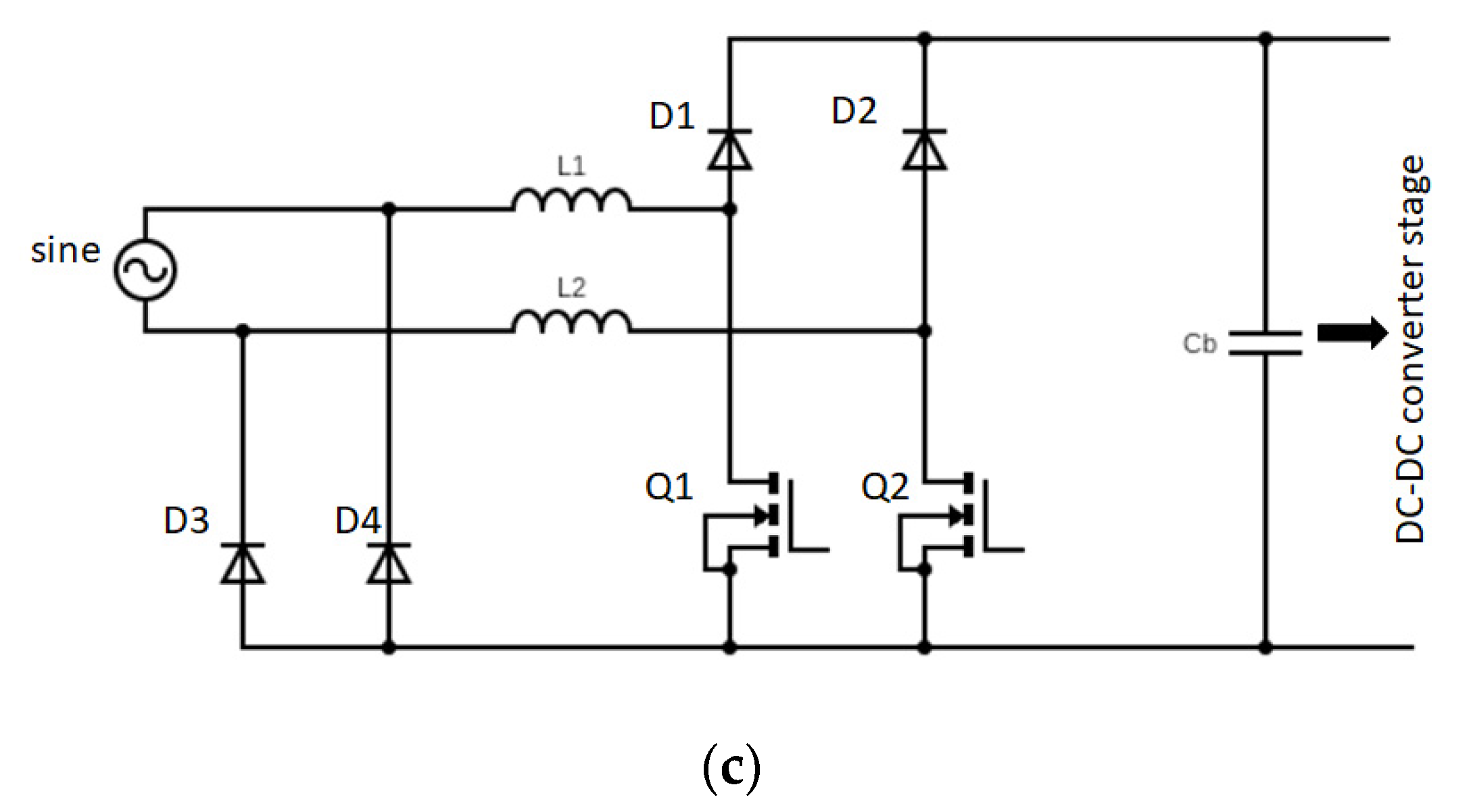
The bridgeless PFC typologies as shown in Figure 2c has higher efficiency as compared with the other PFC topologies since the input bridge rectifier is not used. However, most of these bridgeless topologies experience a higher level of EMI [19]. Different modifications and types of bridgeless topologies with complex design and higher costs are implemented to decrease these EMI issues [19,20,21,22]. Therefore, the use of the bridgeless PFC topology is limited in the telecom power applications, where the EMI level requires to be at the lower limits. For this reason, and to optimize the economic design for the PFC converter, the bridgeless PFC topology was excluded from the analysis, and the comparison in this work and the design analysis of the conventional and the interleaved PFC topologies are, only, performed.
The control circuits of the PFC circuits which implemented based on the boost converter technique usually contains two control loops [23,24,25]: the outer voltage loop, which regulate the output voltage value as the specified load value, and the inner current loop to make the AC supply current follow the AC supply voltage and regulate the circuit PF to higher values. Usually, these control loops in analogy control circuits are implemented using proportional-integral (PI) controllers [26,27,28]. The parameters of the PI controllers implemented to work with the boost converters are usually optimized by deriving the converter operation equations and linearized the system with using the different linearization techniques. Practically, PFC control circuits can be implemented using integrated circuits (IC) control chips such as the conventional PFC control IC’s (UCC28180, UCC29950), and interleaved PFC control IC’s (UCC28070, UCC28065) from Texas Instruments (Dallas, Texas, USA) (, country) [29]. The adjustment of the voltage and current control loops in these control IC’s is performed by deriving the linearized small signal modeling of the converter system and choosing the closed loop control system stability criteria which are specified by the control system crossover frequency and the damping ratio [15,24,30,31].
The target of this study was to study the optimal design, manufacturing of the conventional and interleaved PFC with the high-power density and verified the performance of both topologies using the simulation and the experimental implementation. The performance of both PFC topologies was investigated by optimizing the parameters of the boost converter voltage and current control loops based on obtaining the proposed small signal stability modeling for both topologies and using the proper stability criterion for the closed loop control loops. The main parts of the power and control circuits in the two topologies were designed for the enhancement of the circuit high power factor, good conversion efficiency, a specified level of the load voltage, and current ripple contents, and the lower values of the THD follows the telecom power applications load class in the standard EN61000-3-2 [32]. The gains of the current-voltage controllers in both topologies have been optimized to adjust the controller’s crossover frequency and damping ratio.
PSIM simulations have been used to test the performance of the designed PFC converters with the designed components and optimized control loops. Furthermore, the design of the printed circuit board (PCB) for both topologies using the OrCAD(, city and country) capture and ALEGRO PCB (Cadence 17.4, California, USA) (version, city and country) design software to verify the experimental performance and to make the comparative analysis between the designed PFC converters performances with different loading conditions are performed.
The following sections in this paper are organized as follows: Section 2 outlines the PFC converters magnetic parts manufacturing and switching elements selection methodology. Section 3 proposed the small signal modeling and the design techniques of the control loops for the different topologies of the PFC converters. Section 4 provides the simulation procedure and results for the different PFC topologies employed. Section 5 shows the printed circuit board (PCB) design, provides the experimental verification, and the comparative analysis of the performance for the different PFC topologies. Section 6 is the conclusion of the paper.
2. PFC Converters Power Components Design Analysis and Selection
As shown in the different PFC topologies depicted in Figure 2, the principle operation of the different PFC topologies is based on the boost converter operation. The three main power elements in such these converters to be designed are, (1) the storage energy element represented by the boost inductor (Lb), (2) selecting the switching parts represented by the high voltage Mosfet (Qb) and the high current fast switching diode (Db), and (3) the design of the output filter represented by the output bulk capacitor (Cb) connecting in parallel with the high voltage output side. The following subsections outline the design analysis of the boost converter’s different power components for the conventional and the interleaved PFC boost converters topologies.
2.1. The Boost Inductor Design and Manufacturing
2.1.1. Conventional PFC Boost Inductor
There are many considerations to consider when selecting the PFC boost inductors, such as the inductance value, the direct current resistance (DCR), and the saturation current value. The first step to designing the required boost inductor is to calculate the required inductance value based on the required circuit ripple current which is usually calculated as the percentage (10–40%) of the maximum input current to the boost converter [33].
For the conventional CCM PFC, the boost inductor value can be expressed as given [5]:
Where Vin_min is the minimum supply input voltage, %Ripple is the inductor ripple current percentage, η is the desired efficiency, Po is the power rating, and Fsw is the converter switching frequency.
The circuit operation of the conventional PFC boost converter working in the continuous current conduction mode (CCM) can be represented by two operation modes. Figure 3 depicts the waveforms of the inductor voltage and currents for the boost converter at different operation modes, where VL represents the inductor voltage, IL represents the inductor current, D is the converter duty cycle, Ton is the on-switching time, Toff is the off-switching time, Ts is the switching time, Vin is the boost converter input voltage, Vo is the output voltage, and ΔILrpp is the inductor ripple current peak to peak value.
Mode-1, when the switch (Qb) is closed, the energy is stored in the inductor, generating a magnetic field. Mode-2, when Qb is opened, the current circuit impedance increases, thereby reducing the current, and the magnetic field previously created is reduced to let the current toward the load, thus, the inductor voltage polarity is reversed, which places the two sources in series, and charging the capacitor (Cb) through the fast switching diode (Db).
The boost converter average input current is the same as the inductor average current (Iavg) which can be calculated at full load condition and rated output voltage as given
The boost converter is designed to work with supply voltage wide range (85–265) V. So, the maximum and the minimum duty cycle values are calculated as
The average inductor currents at minimum and maximum supply voltage are calculated as
The inductor ripple current as the percentage (%Ripple) of the converter total input current can be expressed as
From (4) and (5), and from the waveforms in Figure 3, the inductor maximum peak current is calculated as
Using the converter parameters given in Table 1, the required inductance, and the inductor maximum peak current for the conventional CCM PFC converter can be calculated. Based on the calculated inductance and the inductor current, the inductor core, the number of turns (N), and the size of the winding wire have to be selected.
The PFC inductor core was designed to have a high saturation level which prevents the saturation at the maximum peak current (IL_pk), support the converter operation with the designed switching frequency, also, the inductor core losses have to be accepted in accordance with the temperature rise during the PFC converter operation. Kool Mu core material’s with low loss, relatively high saturation level (10,500 gausses), higher switching frequency level up to 200 kHz, and the near-zero magnetostriction (ability to expand or contract in response to a magnetic field) make the Kool Mµ material good for eliminating audible frequency noise in in-line noise filters and inductors, which also make it excellent for the implementation of the PFC circuits [34].
Choosing the inductor core in this work will be conducted by using the LI2 method to choose the core part number from the Kool Mu chart of the Magnetic inc supplier, as shown in Figure 4, where L is the inductance value and I is the inductor average current. [34,35].
From the chart and with using the calculated value of the LI2, and take in account offering the required value of the inductance with the suitable space for the wire winding around the core, the conventional PFC converter inductor is designed with using two stacked Kool Mu Toroids core with part number of 77083A7. The inductor number of turns (N) to obtain the required inductance value (Lb) can be calculated as:
where AL_min is the minimum inductance factor for each core (AL_min = 74.52 nH/T2).
The copper loss of the winding wire can be calculated on maximum value of the rms input current (Iin_rms) as given
where DCR is the inductor wire DC resistance and PF is the designed converter power factor.
The inductor wire which is selected based on the inductor maximum peak current, and should meet the requirements that it should be thick so that the DCR is small and it should be possible to form the required number of turns around the core. In this work, the conventional CCM PFC inductor was manufactured with 60 turns of the copper wire with 1.15 mm diameter size around the 2-stacked Kool Mu 77083A7 toroids cores. The manufactured inductor DCR value was experimentally measured, and it was about 0.087 Ω.
2.1.2. Interleaved PFC Boost Inductor
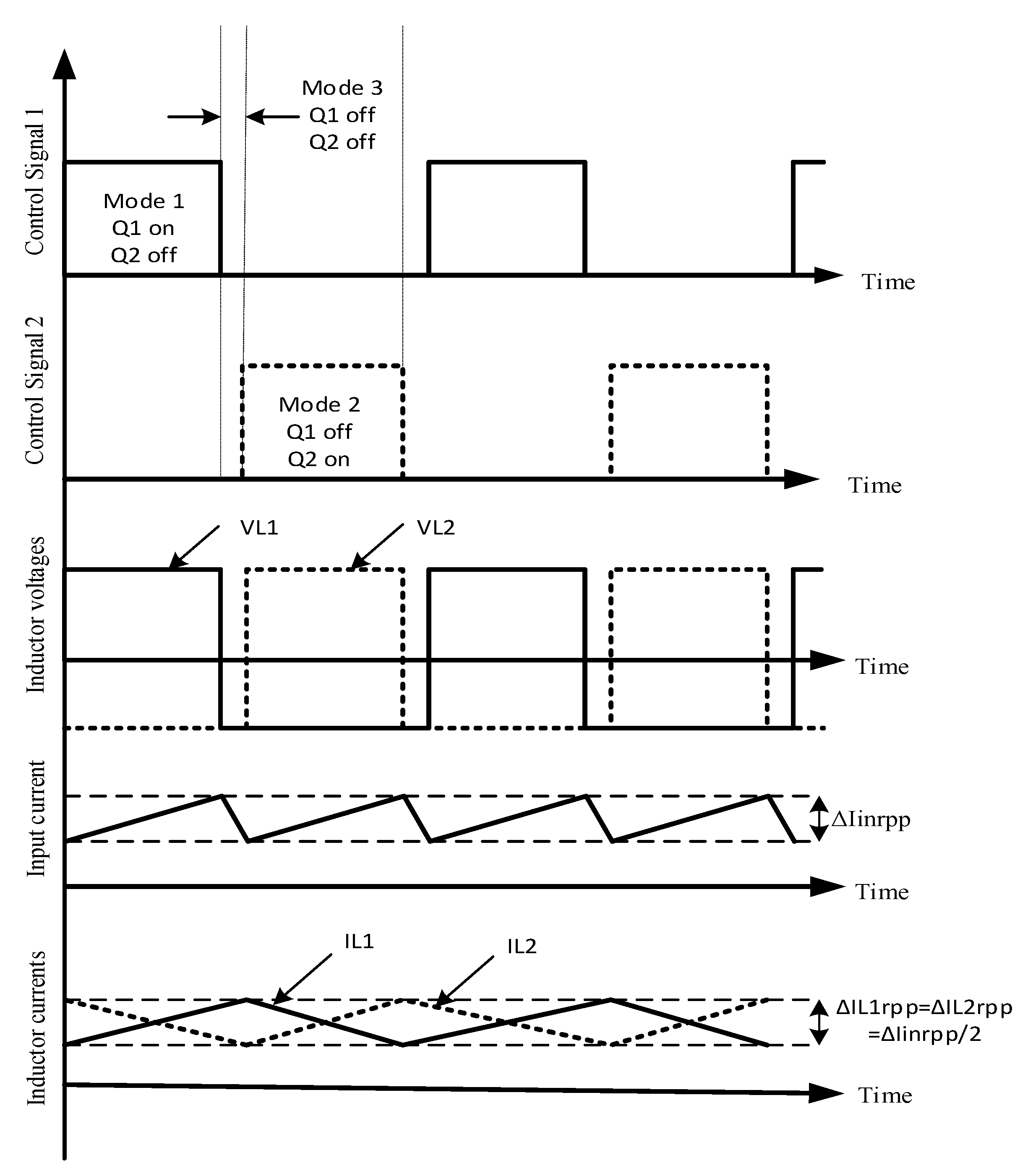
In the interleaved PFC converter, the total power is shared among the parallel channels and the PWM signals for each channel switch are at 360/n, where n is the channels number. A 2-channel interleaved CCM PFC topology is employed in this work. Since this topology uses two inductors, L1 and L2, each with approximately half the size of the conventional boost PFC, so that the thermal performance of the converter will improve [36]. Furthermore, the inductor current ripple in the conventional boost PFC is the same as the input current ripple while in the interleaved boost PFC, the ratio of the boost converter input ripple current to inductor’s ripple current can vary depending on the duty cycle (D) as given in Equation (7), where the current ripple cancellation in the input side of interleaved type is considered as the major advantage over the conventional type as seen at the input current ripple of the converter in Figure 5 [37].
As the result of the input current ripple cancellation, the size of the EMI filter can be reduced, and the required boost inductors (L1 and L2) values will be reduced which leads to reducing the volume and weight of the designed boost inductors.
The circuit operation of the designed interleaved PFC boost converter working in the continuous current conduction mode (CCM) can represent four operating modes and if the average duty cycle is less than 0.5, both switches will not be turned on at the same time which results in three operating modes describes the on-off states of the 2-channels switches as depicted in the converter waveforms in Figure 6, where VL1, VL2 represents the inductors voltages, and IL1, IL2 represents the inductors currents.
The inductor ripple current at each channel as the percentage (%Ripple) of the converter total input current can be given as
The peak current passing through the inductor at each channel can be given as
using the converter parameters given in Table 1, the required inductance and the inductor maximum peak current for the interleaved CCM PFC converter can be calculated.
For each channel, in order to offer the required value of the inductance with the suitable space of the wire winding around the core, the core of Kool Mu material with part number of 77354A7 was used as depicted in the chart in Figure 4, the inductor number of turns (N) to obtain the required inductance value (L1) and (L2) can be calculated as:
where AL_min is the minimum inductance factor for the chosen core (AL_min=69.92 nH/T2).
The copper loss of the winding wire resistance (DCR) can be calculated on Iin_rms as given
where DCR is the direct current resistance of the inductors L1 and L2.
In this work the interleaved CCM PFC inductors in each channel are manufactured with 65 turns of the copper wire with 0.75 mm diameter size around the single Kool Mu 77354A7 toroids core. The manufactured inductor DCR value was experimentally measured, and it was about 0.055 Ω.
Table 2 shows the comparison between the boost inductor specifications designed for the conventional and the interleaved CCM PFC converters. The view of the manufactured boost inductors for both topologies is shown in Figure 7. From the manufactured boost inductors specifications and the view for both topologies, the reduction in the boost inductor weight, size, and cost can be observed in case of the interleaved topology as compared with the conventional topology.
2.2. Output Capacitor Selection
For both topologies, the design techniques of the output capacitor are the same. The output capacitor value usually calculated to meet the specified output voltage ripple using (14), also, this value should be enough to deliver the output minimum voltage hold up with the specific time (thold), as given in (15)
where Vrpp is the peak to peak output voltage ripple. The larger value among the two equations was selected to design the output capacitor.
The capacitor rms current across the 60 Hz line cycle is given as [40]
The capacitor equivalent series resistance (ESR) is calculated as
where DF is the chosen capacitor dissipation factor and can be obtained from the capacitor datasheet.
The ESR losses of the capacitor can be calculated as
An important issue when choosing the output bulk capacitor for the conventional CCM PFC topology is that the ESR should be as small as possible, as it affects power efficiency and voltage regulations. A larger ESR presents more ripple, affecting the boost converter control loops stability [41]. Usually, aluminum electrolytic capacitors are used where high-power density is required, because of their small volume, these types of capacitors are also preferred in PFC applications since they provide high capacitance value with low equivalent series resistance (ESR), but these capacitor types are expensive when compared with the higher ESR types. On the other hand, the interleaving technique in PFC circuits causes the inductor current ripple reduction and then produces a reduced rms output capacitor current, so capacitors with higher ESR (lower cost) can be used.
2.3. Switching Elements Selection
2.3.1. Power Mosfet Switches Selection
The power Mosfet switches in the PFC boost converters are selected based on the maximum peak current with considering the value of the on-state drain-source resistance (Rdson) to reduce the conduction losses.
In the conventional CCM PFC topology, the rms current (IQb) and the maximum peak current stress (IQb_peak) in the switch Qb can be calculated as given in [7,40].
In case of the interleaved CCM PFC topology, the maximum peak current of the switches Q1, Q2 is the half in case of the conventional CCM PFC converter as given
The conduction losses (PQ Loss_cond) of the switches can be calculated at the switch rms current and using the value of the drain-source resistance of a MOSFET switch Rdson at 100 C as given
The switching losses (PQ Loss_swit) are calculated using the rise time (tr) and fall time (tf) of the Mosfet gate and the capacitance losses (Coss) for the chosen switch.
In case of the interleaved PFC, 2 switches were used to implement the two channels boost converter, but the cost of the switching elements is still lower than the conventional topology because low current rating switches can be used. Based on the current and voltage ratings for both topologies and considering the value of the Rdson, the IPZ60R040C7 switch is used for the conventional, and 2 switches of IPW60R099P6 were used for the interleaved PFC boost converters in this work.
2.3.2. Fast Switching Boost Diode Selection
The boost diode maximum current is calculated as the maximum load current at the minimum output voltage.
In the conventional PFC converter, the boost diode Db maximum current is calculated at the full load condition and minimum output voltage as follow
For the interleaved PFC converter
The diode losses are estimated based upon the forward voltage (Vf) at 125 °C and the reverse recovery charge (Qrr) of the diode.
As given in (26) the boost diode has big influence on the system’s performance due to the reverse recovery behavior. So, the Ultra-fast diode with very low reverse recovery time (trr) and reverse recovery charge (Qrr) is necessary to reduce the switching loss.
In this work Schottky diode is used as the boost diode, the new diode technology of silicon carbide (SiC) Schottky diode with part number of (IDH16G65C5) shows its outstanding performance with almost no reverse recovery behavior. So that, the switching loss due to this diode can be ignored, and only the conduction loss due to Vf is considered.
3. The Proposed Average Small Signal Modelling and Control Circuits Design
To simulate the different PFC topologies for investigating the converter performance with the designed power components, the converter control circuit parameters have to be optimized. The analog PI controllers are used to implement the voltage and current control circuits in the different PFC topologies. The controller’s parameters are obtained with using the proposed average small signal stability modeling for both of the conventional and interleaved CCM PFC topologies.
3.1. Conventional CCM PFC Topology
The control loops of the conventional CCM PFC converter are implemented with two control loops as depicted in Figure 8, the outer loop which regulate the output voltage level to the desired value, and the inner loop which used to let the input current follows the reference current to reduce the inductor current distortion and provide input power with high power factor. The mathematical equations which describe the change in the inductor current (ILb) and output voltage (Vo) for the conventional CCM PFC converter shown in Figure 2a can be given as
where R is the load resistance in ohms.
Assume all variables are at the steady state at the selected operational point and the small-signal AC variation (, where
The designed PFC control system should track and modify the duty cycle (D) based on the small-signal AC variation to regulate Vo and ILb.
Substituting Equation (29) into (27) and (28), we obtain
Equations (30) and (31) can be re-written again as Equations (32) and (33) using the averaging model which consider that over the switching period in the steady state, the inductor current change, and the capacitor voltage is zero.
Arrange state Equations (34) and (35) in state space matrix form to obtain the state space representation of the small signal stability model for the conventional CCM PFC converter as given
Figure 9 presents the control blocks for the outer and inner control loops of the conventional PFC using the PI controller. The optimal parameters for the PI controllers can be obtained by deriving the voltage and current systems transfer functions using the average signal modelling.
For the voltage control loop; the TF of the outer voltage system Gv(s) in s-domain can be obtained as the output voltage to the inductor current transfer function as (37), and the analog PI controller system can be expressed using the TF GPIv(s) as (38)
where KPv is the proportional gain and KIv is the integral gain of the voltage PI controller.
The closed-loop TF of the outer voltage control loop system (GCLV(s)) can be obtained as
For the current control loop; the TF of the inner current system Gi(s) in s-domain can be obtained as the output voltage to the inductor current transfer function as (40), and the analog PI controller system can be expressed using the TF GPIi(s) as (41)
Since the converter switching frequency (Fsw) was selected as about 100 kHz in this work, for high frequency analysis, the capacitor can be shorted, and the open-loop TF of the inductor current system in Equation (40) can be simplified as
The closed loop TF of the current control loop can be obtained as
Once the transfer functions of the control loops are determined, the PI controllers’ gains can be designed with the standard form of the second order system TF by selecting the proper control system bandwidth and the undamped natural frequency which enhanced the optimal stability criteria. Usually, the bandwidth of the outer voltage loop must be very small to eliminate the harmonics of the output DC voltage reflected by the AC input voltage at 60 Hz [42]. What is more the bandwidth of the inner current loop must be high as compared with the outer voltage control loop to let the inductor current follows the reference current, also the current control loop bandwidth must be less than switching frequency (Fsw) to reject the noise at the switching frequency. In this work, the undamped natural frequency (ξ) was considered to be about 0.707, the closed loop bandwidth of (Wn) was assumed to be about 150 rad/s and 10,000 rad/s for the outer voltage and inner current loops, respectively. For the reliable operation of a controller to offer good performance with different loading condition, the controllers Kp and KI parameters were set to work with the minimum value of the load voltage (Vo) of 320 V with the rated input voltage.
Figure 10 depicts the bode plot of the closed-loop TF of the two control loops, which shows that the current controller offers unity gain for frequencies less than 3 kHz. This current control system, working as a low pass filter, helps to remove the switching frequency noise. Moreover, the voltage controller offers unity gain for frequencies less than 23 Hz. This voltage controller works as a low pass filter to remove the 60 Hz voltage ripple.
3.2. Interleaved CCM PFC Topology
The average small signal modelling of the interleaved PFC can be derived in the same way as explained for the conventional boost PFC using state space averaging technique. The interleaved PFC contains two separates boost PFC converters operating 180 degrees out of phase. These two separate legs are assumed to operate identically to derive the transfer function of the model as depicted in Figure 11.
The mathematical equations which describe the change in inductors currents (IL1, IL2) and the output voltage (Vo) can be given as
Assume all variables are at the steady state at the selected operational point and the small-signal AC variation (, where
Substituting from (47) in Equations (44)–(46), we obtain
Equations (48)–(50) can be re-written again as Equations (51)–(53) using the averaging model as follow
Arrange state Equations (51)–(53) in state space matrix form to obtain the state space representation of the small signal stability model for the interleaved CCM PFC converter as given
The transfer function (TF) of the output voltage control system for the interleaved CCM PFC converter can be obtained as given
The transfer function (TF) of the inner current control loops for the inductor’s currents IL1 and IL2 for the interleaved CCM PFC converter can be obtained as given
After rearranging Equation (56), the open loop TF of the inductors currents systems can be written as
For the interleaved CCM PFC converter, the closed loop bandwidth values were assumed to be about 150 rad/s and 18,000 rad/s for the outer voltage and inner current loops, respectively.
Figure 12 depicts the bode plot of the closed-loop TF of the control loops, which shows that the current controller offers unity gain for frequencies less than 5.5 kHz. This current control system, working as a low pass filter, helps to remove the switching frequency noise. Furthermore, the voltage controller offers unity gain for frequencies less than 21 Hz. This voltage controller works as a low pass filter to remove the 60 Hz voltage ripple.
4. Simulation Results
Figure 13 shows the PSIM software (Powersim, Rockville, USA) simulation circuits for the conventional and interleaved PFC circuits with the designed power components values. The EMI filter in both topologies was designed as an LC filter with common mode coupling inductor of about 2.4 mH and suppression capacitors of about 2.2 nF [43]. For the practical simulation results, which were closest to the experimental results, the boost diode is considered as SiC Schottky diode to ignore the switching losses, the forward voltage of the boost diode is about 1.5 V, and the parameters of bridge diode, the boost converter switches for both topologies are obtained from the datasheets of the selected components.
At the rated input of (220 Vrms, 60 Hz) and rated load of Po = 2000 W and Vo = 400 V, the power performance for both topologies is simulated. Figure 14 and Figure 15 show the waveforms of the input and output currents and input and output voltages as well as the circuit power factor (PF) for the conventional and the interleaved CCM PFC converters respectively. We observed that the designed conventional PFC converter offers input power factor at full load condition of 2 kW with minimum value about 0.9955 and maximum value about 0.9970. On the other hand, the interleaved converter offers a power factor with a minimum value of about 0.9975 and a maximum value of about 0.9991 during the full load operating condition. The peak to peak ripple value in the output voltage is measured of about 12.00 V in the conventional and 12.10 V in the interleaved converter which is less than the design specified value (Vrpp = 20 V) for the output voltage ripple contents in both topologies. Additionally, the output ripple current peak to peak value is measured of about 0.153 A in the conventional and 0.151 A in the interleaved converter which is less than 4% in both topologies.
To show the operation performance of the designed current control loops for both PFC topologies, the operation waveforms of inductor currents and the reference current are simulated. Figure 16 and Figure 17 show the inductor’s current and the reference current generated from the outer voltage control loop for the conventional and the interleaved PFC converters, respectively. It can be observed that the inductors currents successfully follow the reference current in both topologies which ensure input current follows input voltage, and offer higher input power factor values.
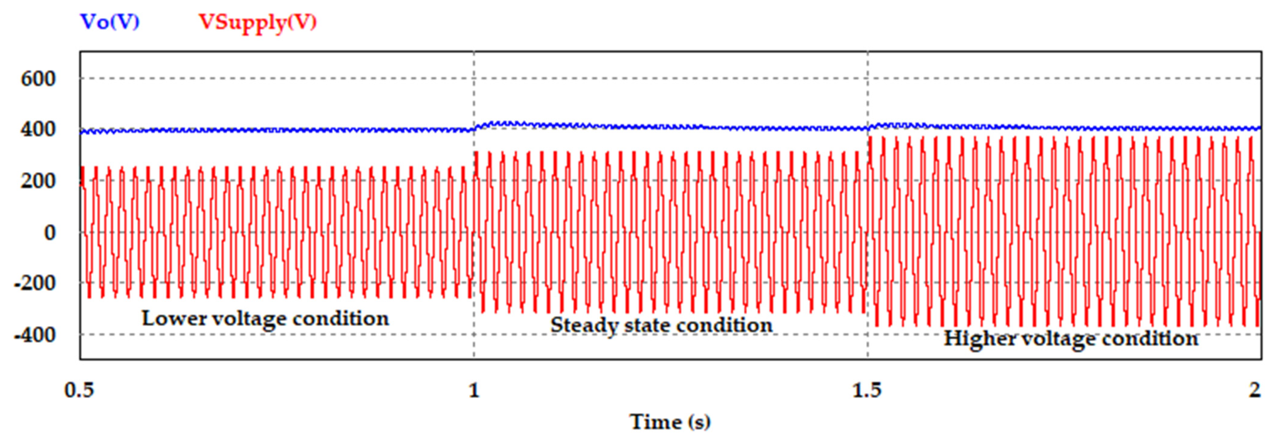
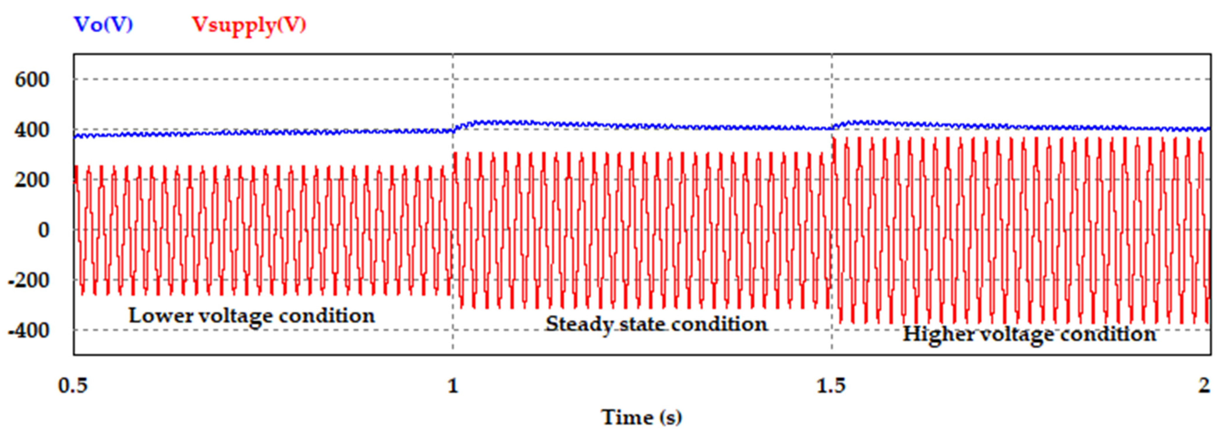
The dynamic performance of the outer voltage control loop to regulate the output voltage to the specified value (400V) with different input voltage conditions is simulated as shown in Figure 18 and Figure 19 for the conventional and the interleaved PFC converters, respectively. Three operation conditions of the lower voltage, steady state voltage, and higher voltage conditions of the input supply voltage are used to test the operation of the outer voltage control loop. It can be observed that the designed outer voltage control loops based on the proposed small signal stability modeling succeed to regulate the output voltage to the specified value with very small transition time with different wide range of the input voltage conditions.
To investigate the advantage of the current ripple cancellation in the interleaved PFC converters over the conventional PFC converters, the input current ripple for both converters is measured at the same switching period from 1.999925 to 1.999985. Figure 20 shows the waveforms of the boost converter input current and inductors currents for the conventional and the interleaved PFC converters. The total input ripples current peak to peak over this switching period is measured for both topologies, which is about 0.6901A for the conventional PFC converter and is reduced to about 0.3091A for the interleaved PFC converter due to the ripple current cancellation of the interleaved converters, reducing of the input current ripples leads to reducing the current total harmonic distortions and increasing the input supply power factor.
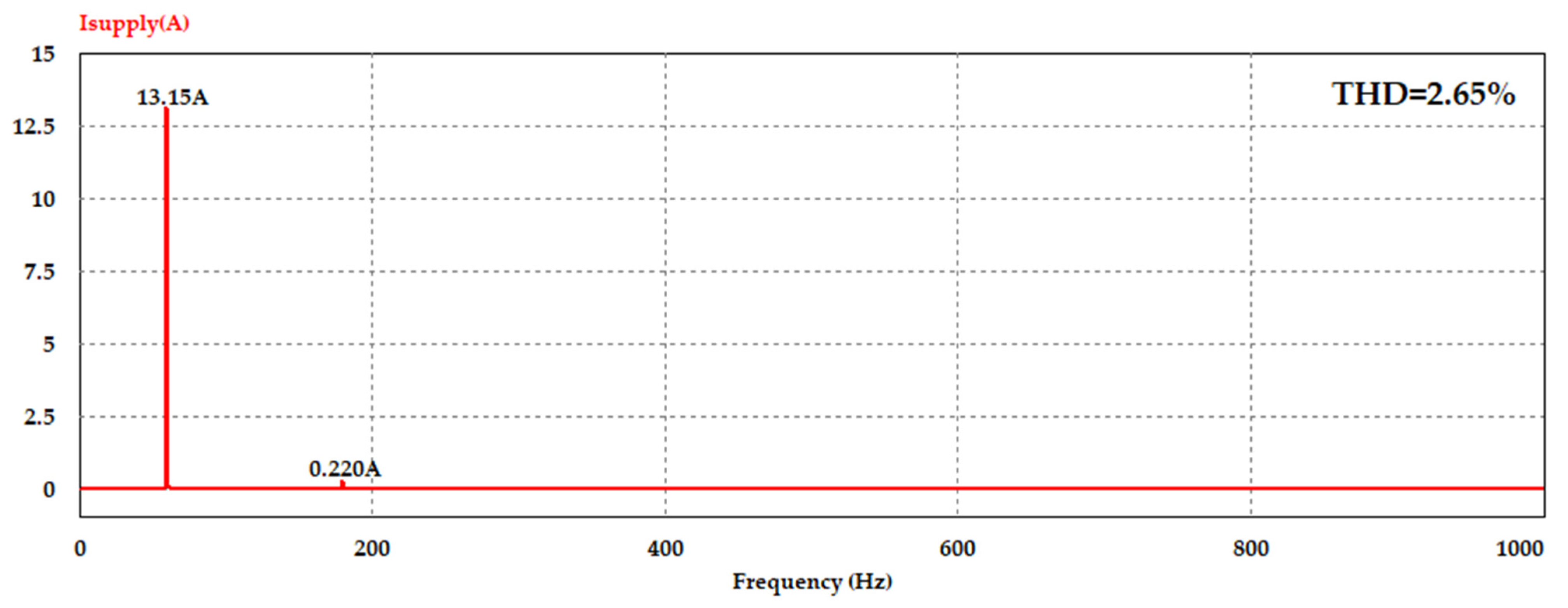
Figure 21 and Figure 22 shows the Fourier analysis for the input current at the full load condition of the conventional and the interleaved CCM PFC converters, respectively. It is observed that the third harmonic is the dominant harmonic in the current spectrum and it is about 0.578 A for the conventional PFC, which reduced to about 0.220 A with the interleaved PFC converter. Furthermore, the total harmonic distortion (THD) of about 4.67% in the conventional PFC converter and reduced to about 2.65% with the interleaved PFC converter. It can observe that the designed PFC converters offer harmonic level follows the harmonic standard specification IEEE 519-20142 [35] and IEC 61000-3-2 [36] for the design of the telecom power supply.
5. Experimental Verification
The printed circuits board (PCB) for the 2 kW PFC converters is designed using OrCAD capture and PCB design software 17.4 (Cadence, California, USA) using the components given in Table 3. The control circuit for the conventional PFC circuit is implemented using the UCC28180 CCM PFC controller and the control circuit for the interleaved PFC circuit is implemented using the UCC28070 interleaved CCM PFC controller from Texas instruments. With using the design calculation tools of both IC controllers, the cross over frequency for the voltage and current control loops are adjusted with the same values given in design Section 3.
Figure 23 shows the experimental setup used for testing the experimental performance for the designed PFC converters. The Kikusi DC electronic load with a power rating of about 3 kW is used for loading the converters from 25% to 100% of the full load condition.
At the rated input of (220 Vrms, 60 Hz), different loading conditions (25%, 50%, 75%, and 100%) of the full load condition are loaded to the designed converter. Figure 24 and Figure 25 and show the input, output voltages, input current waveforms, and the power factor measurement for the conventional and the interleaved PFC converters, respectively.
It is observed that the designed voltage control loops in the conventional and interleaved PFC converters ables to adjust the output voltage at a constant value of 400 V with very small ripple contents at different loading conditions. Additionally, the current control loops offer input current with a high power factor and small THD. Figure 24a shows that the conventional PFC converter offers an input power factor of about 98.8% at a lower loading condition of 25%, which is higher than an interleaved PFC converter of 97.50% with the same loading condition as shown in Figure 25a.
With the increasing of the loading condition in the conventional PFC converter, the input current distortion factor is increased due to the high voltage and current stresses in the PFC converter switch and increasing of the thermal heating of the PFC inductor which reduced the input power factor at higher loading condition. On the other hand, the channeling of the current through two channels in the interleaved PFC converter reduced the components’ current and voltage stresses and also improve the thermal performance of the PFC inductors, makes the converter power factor stable at higher values at the higher loading condition. At full loading condition of 2 kW, Figure 24d and Figure 25d show that the conventional PFC converter offers an experimentely power factor value about 99% and the interleaved PFC converter offers a power factor value of about 99.85%.
With different loading conditions, as depicted in Figure 26, the designed PFC converters performances are tested through measurements of the THD, power factor and conversion efficiency by using the simulation and experimental tests. At 25% loading condition the efficiency of the conventional PFC converter is experimentally about 95.9% and for the interleaved PFC converter is about 93.8%, when the load is increased to about 100% loading condition, the conventional PFC converter efficiency is about 97%, and for the interleaved PFC converter is about 97.6%. It is observed that, at a low loading condition the conventional PFC converter offers higher efficiency than the interleaved converter, but when the loading power is increased the current stress and thermal losses in the conventional PFC boost inductor and Mosfet is increased which increased the thermal power losses and reduced the conversion efficiency, also increasing the current distortion factor, increasing the THD, and reducing the input power factor.
On the other hand, interleaving technique in the PFC converters improve the converter thermal performance, reducing the voltage, and current stresses in the boost converter components at higher loading condition which increase the conversion efficiency, and reducing the total harmonic distortion of the input current at high power loading condition as shown in Figure 26c, where the THD is reduced from 5.6% in the conventional PFC converter to about 3.2% with using of the interleaved PFC converter. Usually, in the PFC converter circuits, the input power factor is depending on the displacement factor and the distortion factor [5], thus, reducing the current distortion factor leads to an increase in the input power factor from 99% to about 99.85% as shown in Figure 26a.
6. Conclusions
In this paper, the detailed design analysis and manufacturing of the printed circuit board (PCB) of two topologies of the telecom PFC converters with high-power density, high conversion efficiency, high input power factor, and lower THD are performed. The proposed small signal modeling is used to design the parameters of the PI controllers for the current and voltage control loops for both topologies. Simulation and experimental tests are used to test the performance of the designed converters with different loading conditions. The simulation and experimental results show that the conventional PFC topology with the proposed design offers higher efficiency and higher power factor at lower loading condition until 800 W as compared with the interleaved PFC converter, but when the loading condition is increased more than 800 W, the thermal heating in the conventional boost inductor, the boost diode, and Mosfet is increased leading to higher conduction losses and higher current distortion factor which reduced the conversion efficiency and, also, reduced the input power factor.
The experimental results show that, at the higher loading condition, the efficiency of the designed interleaved boost PFC converter is higher as compared with the conventional boost PFC converter since the power is channeled through two paths which reduced the boost inductor size and weight. Furthermore, the interleaving technique reduces the voltage and current stresses across the Mosfet switches and improves the component’s thermal performance, improvement of the converter thermal performance decreases the conduction losses of the inductor, the boost diode, and the Mosfet, increased the conversion efficiency and input power factor with higher loading condition.
Author Contributions
A.H.O. created, designed and applied the proposed controlling technique. The literature review and manuscript preparation, as well as the simulations, were carried out by A.H.O. Experimental verification was carried out by A.H.O. and J.B. Final review of manuscript corrections was conducted by J.B. All authors have read and agreed to the published version of the manuscript.
Funding
This research was funded by grant (2018R1D1A3B0704376414) from National Research Foundation of Korea (NRF), grant (21RTRP-B146046-04) from Railroad Technology Research Program (RTRP) funded by Ministry of Land, Infrastructure and Transport of the Korean government and research grant from Hyundai Motor Group.
Data Availability Statement
Not applicable.
Conflicts of Interest
The authors declare no conflict of interest.
References
- Kim, Y.; Sung, W.; Lee, B. Comparative Performance Analysis of High Density and Efficiency PFC Topologies. IEEE Trans. Power Electron. 2014, 29, 2666–2679. [Google Scholar] [CrossRef]
- Chen, Z.; Davari, P.; Wang, H. Single-phase bridgeless PFC topology derivation and performance benchmarking. IEEE Trans. Power Electron. 2020, 35, 9238–9250. [Google Scholar] [CrossRef]
- Kim, Y.S.; Lee, B.K.; Lee, J.W. Topology characteristics analysis and performance comparison for optimal design of high efficiency PFC circuit for telecom. In Proceedings of the 2011 IEEE 33rd International Telecommunications Energy Conference (INTELEC), Amsterdam, The Netherlands, 9–13 October 2011; pp. 1–7. [Google Scholar]
- Okilly, A.H.; Kim, N.; Baek, J. Inrush Current Control of High-Power Density DC–DC Converter. Energies 2020, 13, 4301. [Google Scholar] [CrossRef]
- Okilly, A.H.; Jeong, H.; Baek, J. Optimal IP Current Controller Design Based on Small Signal Stability for THD Reduction of a High-Power-Density PFC Boost Converter. Appl. Sci. 2021, 11, 539. [Google Scholar] [CrossRef]
- Xiong, Y.; Huang, Y.; Zhong, Z.; Zhang, T. Research and design on digital PFC of 2kW On-board charger. World Electr. Veh. J. 2010, 4, 202–207. [Google Scholar] [CrossRef] [Green Version]
- Basic Calculation of a Boost Converter’s Power Stage. Application Report, Texas Instruments. Dallas, TX, USA. January 2014. Available online: https://www.ti.com/lit/pdf/slva372 (accessed on 9 April 2021).
- Chitra, P.; Seyezhai, R. Basic design and review of two phase and three phase interleaved boost converter for renewable energy systems. Int. J. Appl. Sci. 2014, 1, 1–26. [Google Scholar]
- Yang, F.; Li, C.; Cao, Y.; Yao, K. Two-phase interleaved boost PFC converter with coupled inductor under single-phase operation. IEEE Trans. Power Electron. 2019, 35, 169–184. [Google Scholar] [CrossRef]
- Wu, H.; Pickert, V.; Giaouris, D.; Ji, B. Nonlinear analysis and control of interleaved boost converter using real-time cycle to cycle variable slope compensation. IEEE Trans. Power Electron. 2016, 32, 7256–7270. [Google Scholar] [CrossRef]
- Narula, S.; Singh, B.; Bhuvaneswari, G.; Pandey, R. An interleaved PFC converter-based welding power supply with improved power quality. In Proceedings of the 2016 IEEE 6th International Conference on Power Systems (ICPS), New Delhi, India, 4–6 March 2016; pp. 1–6. [Google Scholar]
- Huber, L.; Jang, Y.; Jovanovic, M.M. Performance Evaluation of Bridgeless PFC Boost Rectifiers. IEEE Trans. Power Electron. 2008, 23, 1381–1390. [Google Scholar] [CrossRef]
- Tseng, S.-Y.; Fan, J.-H. Bridgeless Boost Converter with an Interleaving Manner for PFC Applications. Electronics 2021, 10, 296. [Google Scholar] [CrossRef]
- Li, G.; Xia, J.; Wang, K.; Deng, Y.; He, X.; Wang, Y. A single-stage interleaved resonant bridgeless boost rectifier with high-frequency isolation. IEEE J. Emerg. Sel. Top. Power Electron. 2019, 8, 1767–1781. [Google Scholar] [CrossRef]
- Masresha, H.; Haile, T. Investigation of Optimized Topology for AC/DC Power Supply Unit in Telecom Industry. Master’s Thesis, Chalmers University of Technology, Göteborg, Sweden, 2019. [Google Scholar]
- Rosas-Caro, J.; Escobar, G.; Valdez-Resendiz, J.E.; Maldonado, J.C.; Beltran-Carbajal, F.; Del-Valle-Soto, C. Analysis of the Input Current-Ripple in the Series-Capacitor Boost Converter. IEEE Trans. Ind. Electron. 2020, 68, 10303–10308. [Google Scholar] [CrossRef]
- Ibarra-Nuño, C.; Rodríguez, A.; Alejo-Reyes, A.; Cuevas, E.; Ramirez, J.M.; Rosas-Caro, J.C.; Robles-Campos, H.R. Optimal Operation of the Voltage-Doubler Boost Converter through an Evolutionary Algorithm. Mathematics 2021, 9, 423. [Google Scholar] [CrossRef]
- Villarreal-Hernandez, C.A.; Loranca-Coutiño, J.; Mayo-Maldonado, J.C.; Valdez-Resendiz, J.E.; García-Vite, P.M.; Valderrabano-Gonzalez, A.; Rosas-Caro, J.C. A Double Dual Boost Converter with Switching Ripple Cancellation for PEMFC Systems. Electronics 2020, 9, 1592. [Google Scholar] [CrossRef]
- Kong, P.; Wang, S.; Lee, F.C. Common Mode EMI Noise Suppression for Bridgeless PFC Converters. IEEE Trans. Power Electron. 2008, 23, 291–297. [Google Scholar] [CrossRef]
- Nasir, J.C. Mitigation of Common Mode Noise for PFC Boost Converter by Balancing Technique. In Proceedings of the 8th IET International Conference on Power Electronics, Machines and Drives (PEMD), Glasgow, UK, 19–21 April 2016. [Google Scholar]
- Mathur, P.; Raman, S. Electromagnetic interference (EMI): Measurement and reduction techniques. J. Electron. Mater. 2020, 18, 1–24. [Google Scholar] [CrossRef] [Green Version]
- Frgal, P. Average Current Mode Interleaved PFC Control; Application Note, Rev. 0; Freescale Semiconductor, Inc.: Austin, TX, USA, 2016; p. 2016. [Google Scholar]
- Cao, G.; Kim, H.J. Improved bridgeless interleaved Boost PFC rectifier with optimized magnetic utilization and reduced sensing noise. J. Power Electron. 2014, 14, 815–826. [Google Scholar] [CrossRef] [Green Version]
- Rashmi, R.; Lembhe, A.; Kharade, P.A.; Uplane, M.D. Current controlled single-phase interleaved boost converter with power factor correction. Int. J. Adv. Res. Electr. Electron. Instrum. Eng. 2016, 5, 3007–3013. [Google Scholar]
- Baek, J.; Park, M.-H.; Kim, T.; Youn, H.-S. Modified Power Factor Correction (PFC) Control and Printed Circuit Board (PCB) Design for High-Efficiency and High-Power Density On-Board Charger. Energies 2021, 14, 605. [Google Scholar] [CrossRef]
- Rasoulinezhad, R.; Abosnina, A.A.; Khodabakhsh, J.; Moschopoulos, G. An AC-DC Interleaved ZCS-PWM Boost Converter with Reduced Auxiliary Switch RMS Current Stress. IEEE Access 2021, 9, 41320–41333, Losses calculation. [Google Scholar] [CrossRef]
- Nussbaumer, T.; Raggl, K.; Kolar, J.W. Design Guidelines for Interleaved Single-Phase Boost PFC Circuits. IEEE Trans. Ind. Electron. 2009, 56, 2559–2573. [Google Scholar] [CrossRef]
- Aiello, G.; Cacciato, M.; Messina, S.; Torrisi, M. A high efficiency interleaved PFC front–end converter for EV battery charger. Commun.-Sci. Lett. Univ. Zilina 2018, 20, 86–91. [Google Scholar]
- Power Factor Correction (PFC) Controllers—Products. Website. Available online: https://www.ti.com/power-management (accessed on 22 January 2021).
- Kanaan, H.Y.; Marquis, A.; Al-Haddad, K. Small-signal modeling and linear control of a dual boost power factor correction circuit. In Proceedings of the 2004 IEEE 35th Annual Power Electronics Specialists Conference (IEEE Cat. No. 04CH37551), Aachen, Germany, 20–25 June 2004; Volume 4, pp. 3127–3133. [Google Scholar]
- Barry, B.C.; Hayes, J.G.; Rylko, M.S.; Stala, R.; Penczek, A.; Mondzik, A.; Ryan, R.T. Small-signal model of the two-phase interleaved coupled-inductor boost converter. IEEE Trans. Power Electron. 2017, 33, 8052–8064. [Google Scholar] [CrossRef]
- Institute of Electrical and Electronics Engineers (IEEE). IEEE Recommended Practice and Requirements for Harmonic Control in Electric Power Systems, IEEE Standard 519, 2014; IEEE: Piscataway, NJ, USA, 2014. [Google Scholar]
- PFC Boost Design. Available online: https://www.mag-inc.com/Products/Powder-Cores/Kool-Mu-Cores/PFC-Boost-Design (accessed on 24 March 2021).
- 2015-Magnetics-Powder-Core-Catalog, Core Selector Charts. Available online: https://www.mag-inc.com/getattachment/Products/Powder-Cores/Learn-More-about-Powder-Cores/2015-Magnetics-Powder-Core-Catalog.pdf?lang=en-US (accessed on 19 April 2021).
- Magnetics Powder Cores Molypermalloy, High Flux, Kool Mµ, XFlux Selection Catalogues. Available online: https://www.mag-inc.com/getattachment/Products/Powder-Cores/Learn-More-about-Powder-Cores/2015-Magnetics-Powder-Core-Catalog.pdf?lang=en-US (accessed on 24 January 2021).
- Jang, J.; Pidaparthy, S.K.; Choi, B. Implementation and Evaluation of Interleaved Boundary Conduction Mode Boost PFC Converter with Wide Band-Gap Switching Devices. J. Power Electron. 2018, 18, 985–996. [Google Scholar]
- Gu, Y.; Zhang, D. Interleaved boost converter with ripple cancellation network. IEEE Trans. Power Electron. 2012, 28, 3860–3869. [Google Scholar] [CrossRef]
- Control Integrated Power System (CIPOS™) 2-Phase Interleaved PFC IPM (IFCMxxT65yz) Reference Board; Application Note; Infineon Company: Neubiberg, Germany, 6 June 2018.
- Xu, H.; Chen, D.; Xue, F.; Li, X. Optimal design method of interleaved boost PFC for improving efficiency from switching frequency, boost inductor, and output voltage. IEEE Trans. Power Electron. 2018, 34, 6088–6107. [Google Scholar] [CrossRef]
- UCC28070 300-W Interleaved PFC Pre-Regulator Design Review; Application Report; Texas Instruments: Dallas, TX, USA, 2010; Available online: https://www.ti.com/lit/an/slua479b/slua479b.pdf?ts=1613536856416&ref_url=https%253A%252F%252Fwww.google.com%252F (accessed on 20 August 2021).
- Understanding ESR in Electrolytic Capacitors. Available online: https://www.avnet.com (accessed on 15 April 2020).
- Mejía-Ruiz, G.E.; Muñoz-Galeano, N.; López-Lezama, J.M. Modeling and development of a bridgeless PFC Boost rectifier. Rev. Fac. De Ing. Univ. Antioq. 2017, 82, 9–21. [Google Scholar] [CrossRef] [Green Version]
- 5kW PFC Evaluation Board with CCM PFC Controller ICE3PCS01G; Design Report; Infineon Company: Neubiberg, Germany, 2015; Available online: https://www.infineon.com/cms/en/product/evaluation-boards/eval_2k5w_ccm_4p_v3/ (accessed on 9 April 2021).
Figure 1.
Construction of the industrial high-power density telecom power supply.

Figure 2.
Schematic circuits of the different telecom PFC (power factor correction ) topologies: (a) conventional topology; (b) interleaved topology; (c) bridgeless topology.
Figure 2.
Schematic circuits of the different telecom PFC (power factor correction ) topologies: (a) conventional topology; (b) interleaved topology; (c) bridgeless topology.


Figure 3.
Boost inductor voltage and currents waveforms of the conventional PFC topology.

Figure 4.
Boost inductor core selection for the conventional and the interleaved PFC topologies.

Figure 5.
Normalized input ripple current vs. duty cycle in conventional and interleaved PFC.

Figure 6.
Voltage and currents waveforms of the interleaved CCM (continues-current-conduction mode) PFC topology.
Figure 6.
Voltage and currents waveforms of the interleaved CCM (continues-current-conduction mode) PFC topology.

Figure 7.
The manufactured PFC boost inductors.

Figure 8.
Implementation technique of the conventional CCM PFC analog control circuit.

Figure 9.
Block diagrams of the closed loop control systems: (a) outer voltage loop; (b) inner current loop.
Figure 9.
Block diagrams of the closed loop control systems: (a) outer voltage loop; (b) inner current loop.

Figure 10.
Bode plots for the control loops for the conventional CCM PFC converter: (a) voltage control loop; (b) current control loop.
Figure 10.
Bode plots for the control loops for the conventional CCM PFC converter: (a) voltage control loop; (b) current control loop.

Figure 11.
Implementation technique of the interleaved CCM PFC analog control circuit.

Figure 12.
Bode plots for the control loops for the interleaved CCM PFC converter: (a) voltage control loop; (b) current control loop.
Figure 12.
Bode plots for the control loops for the interleaved CCM PFC converter: (a) voltage control loop; (b) current control loop.


Figure 13.
PSIM simulation circuit for the PFC topologies: (a) conventional boost PFC; (b) interleaved boost PFC.
Figure 13.
PSIM simulation circuit for the PFC topologies: (a) conventional boost PFC; (b) interleaved boost PFC.

Figure 14.
Voltages, currents, and input power factor for the conventional CCM PFC at full load condition.
Figure 14.
Voltages, currents, and input power factor for the conventional CCM PFC at full load condition.

Figure 15.
Voltages, currents, and input power factor for the interleaved CCM PFC at full load condition.
Figure 15.
Voltages, currents, and input power factor for the interleaved CCM PFC at full load condition.

Figure 16.
Inductor current and reference current for the conventional CCM PFC at full load condition.
Figure 16.
Inductor current and reference current for the conventional CCM PFC at full load condition.

Figure 17.
Inductors current and reference current for the interleaved CCM PFC at full load condition.
Figure 17.
Inductors current and reference current for the interleaved CCM PFC at full load condition.

Figure 18.
Output voltage dynamic performance with different input voltage for the conventional CCM PFC.
Figure 18.
Output voltage dynamic performance with different input voltage for the conventional CCM PFC.

Figure 19.
Output voltage dynamic performance with different input voltage for the interleaved CCM PFC.
Figure 19.
Output voltage dynamic performance with different input voltage for the interleaved CCM PFC.

Figure 20.
Input ripple current measurements: (a) conventional boost PFC; (b) interleaved boost PFC.
Figure 20.
Input ripple current measurements: (a) conventional boost PFC; (b) interleaved boost PFC.

Figure 21.
Supply current frequency spectrum for the conventional CCM PFC.

Figure 22.
Supply current frequency spectrum for the interleaved CCM PFC.

Figure 23.
Experimental setup for testing of the designed PFC converters.

Figure 24.
Input and output voltages, input current, and power factor of the designed conventional PFC converter with different loading condition. (a) 25%; (b) 50%; (c) 75%; (d) 100%.
Figure 24.
Input and output voltages, input current, and power factor of the designed conventional PFC converter with different loading condition. (a) 25%; (b) 50%; (c) 75%; (d) 100%.

Figure 25.
Input and output voltages, input current, and power factor of the designed interleaved PFC converter with different loading condition. (a) 25%; (b) 50%; (c) 75%; (d) 100%.
Figure 25.
Input and output voltages, input current, and power factor of the designed interleaved PFC converter with different loading condition. (a) 25%; (b) 50%; (c) 75%; (d) 100%.


Figure 26.
Performance measurements with different loading condition: (a) power factor (PF); (b) conversion efficiency; (c) THD (total harmonic distortions).
Figure 26.
Performance measurements with different loading condition: (a) power factor (PF); (b) conversion efficiency; (c) THD (total harmonic distortions).


Table 1.
The target PFC converters stage design specifications.
| Design Parameter | Value | Unit |
|---|---|---|
| Supply voltage (Vin) | 220 (85–265) | V |
| Supply Frequency (F) | 60 (47–63) | Hz |
| Output Voltage (Vo) | 400 (320–410) | V |
| Output Power (Po) | 2000 | W |
| Efficiency (η) | 95% | - |
| Switching Frequency (Fsw) | 100 | kHz |
| Hold Up Time (thold) | 10 | ms |
| Inductor ripple (%Ripple) | 20% | |
| voltage ripple (Vrpp) | 20 | Vpp |
| Current ripple | 5% |
Table 2.
Boost inductor specifications for the PFC (power factor correction) topologies. CCM (continues-current-conduction mode).
Table 2.
Boost inductor specifications for the PFC (power factor correction) topologies. CCM (continues-current-conduction mode).
| Conventional CCM PFC | Interleaved CCM PFC | |
|---|---|---|
| Inductor No. of units | 1 | 2 |
| Core type | Kool Mu (77083A7) | Kool Mu (77354A7) |
| Inductive factor (AL) | 81 ± 8% (nH/T2) | 76 ± 8% (nH/T2) |
| No. of Turns (N) | 60 | 65 |
| Winding wire | Cupper 1.15 mm | Cupper 0.75 mm |
| DC resistance (DCR) | 0.078 Ω | 0.055 Ω |
| Total Weight | 175 g | 95 g |
| Total cost | 17.00 USD | 11.00 USD |
Table 3.
Selection elements of the different topologies.
| Conventional CCM PFC | Interleaved CCM PFC | |
|---|---|---|
| Bridge | GSIB2580 | GBJ3508 |
| Boost Inductor | 470 uH | 2× 300 uH |
| MOSFET | IPZ60R040C7 | 2× IPW60R099P6 |
| Boost Diode | IDH16G65C5 | 2× IDH16G65C5 |
| Bulk capacitor | 1120 uF (2× EKMR421VSN561MR50S) | 1120 uF (2× ALA7DA561DE450) |
| PFC Control IC | UCC 28180 | UCC 28070 |
| Gate driver | 1ED160N12AF | UCC27324D |
Publisher’s Note: MDPI stays neutral with regard to jurisdictional claims in published maps and institutional affiliations. |
© 2021 by the authors. Licensee MDPI, Basel, Switzerland. This article is an open access article distributed under the terms and conditions of the Creative Commons Attribution (CC BY) license (https://creativecommons.org/licenses/by/4.0/).
Share and Cite
MDPI and ACS Style
Okilly, A.H.; Baek, J. Optimal Design Analysis with Simulation and Experimental Performance Investigation of High-Power Density Telecom PFC Converters. Appl. Sci. 2021, 11, 7911. https://doi.org/10.3390/app11177911
AMA Style
Okilly AH, Baek J. Optimal Design Analysis with Simulation and Experimental Performance Investigation of High-Power Density Telecom PFC Converters. Applied Sciences. 2021; 11(17):7911. https://doi.org/10.3390/app11177911
Chicago/Turabian StyleOkilly, Ahmed H., and Jeihoon Baek. 2021. "Optimal Design Analysis with Simulation and Experimental Performance Investigation of High-Power Density Telecom PFC Converters" Applied Sciences 11, no. 17: 7911. https://doi.org/10.3390/app11177911
Note that from the first issue of 2016, this journal uses article numbers instead of page numbers. See further details here.