1. Introduction
The Micromegas (Micromesh gaseous structure) particle detector was invented in 1995 by I. Giomataris and collaborators [
1]. It is a two-stage parallel plate avalanche chamber with a narrow amplification gap (tens to one or two hundred microns). The gas volume is split between two regions by a thin micromesh, which separates the amplification gap from the drift gap.
Figure 1 shows a sketch of the Micromegas working principle.
To preserve a distance between the anode and the grid mesh, spacers from insulating material are used. Initially, fishing lines, 100 m in diameter were used, which were soon replaced by pillars fabricated with conventional photo-lithography. In the region above the mesh, called the conversion or ionization region, the primary electrons are produced by the conversion of X-rays or by ionization from a charged track. The field in this region ranges generally from 100 V/cm to 10 kV/cm, fixed by the voltage imposed on an electrode (cathode) closing this volume.
The thickness of this region ranges from a few mm for the detection of normally incident tracks to a few meters in the case of a Time Projection Chamber (TPC) [
2,
3]. Electrons produced in the conversion gap by the incident particle are drifting toward the mesh and reach the amplification gap due to the funnel shape of the field lines through the mesh holes. In this region, between the mesh and the anode, a high field of several tens of kV/cm induces multiplication to those ionization electrons. The electric field is homogeneous both in the drift and amplification gaps.
Historically parallel plate detectors used an amplification gap on the order of 4 mm. During the development of another detector called the “Hadron Blind Detector” (HBD) [
4] in 1991, an improvement of the stability of the structure was noticed when using a narrower gap; however, it proved impossible to go below 1 mm due to the defects of parallelism and the traction of the grid toward the plane of the anode by the strong electric field applied. This improvement effect was later understood and put into the form of a simple mathematical equation: due to the narrow amplification region in Micromegas, the variations of the amplification gap (mechanical defects) are compensated by an inverse variation of the amplification coefficient and, therefore, do not cause fluctuations in the gain of the detector [
5]. This is not possible in the case of a large amplification space, such as in traditional parallel plate detectors.
Further improvements and simplifications in the fabrication techniques in the following years led to demonstrating better performance and obtaining outstanding results in the laboratory and in the test beams at the European Laboratory for Particle Physics (CERN): spatial resolution (12
m), temporal (<1 ns) and good resistance at counting rates greater than 10
s
mm
[
6,
7]. Thanks to these advances, the detector was adopted by the international scientific community, and today it is widely used in projects by numerous international collaborations [
8].
The simple concept of the Micromegas detector has many advantages: a low material budget, only two moderate-voltages suffice to operate it, a fast electron signal, efficient and fast ion collection due to the small gap size, high rate capabilities and low space charge build-up, as well as the absence of a ballistic deficit. The small amplification gap is a key element in Micromegas operation, giving rise to a great performance:
Excellent spatial resolution: 12
m (Root Mean Square) (RMS) accuracy (limited by the pitch of the micromesh) was achieved in a beam test at CERN, using anode strips with a pitch of 100
m and a low diffusion CF
/iC
H
(80:20) mixture [
7].
A time resolution of 650 ps (RMS) was achieved with the KABES beam spectrometer of the NA48 experiment [
9]. Micromegas studies with fast CF
-based gases are described in [
10]. Recent developments (presented later in
Section 9) using Cerenkov light converted in solid photocathodes have shown the capability of reaching a time resolution of 24 ps for Minimum Ionizing Particles (MIPs).
An energy resolution of ∼11% (Full Width at Half Maximum) (FWHM) with 5.9 keV photons [
7], which is a result close to the limit imposed by statistical fluctuations, showing that the intrinsic fluctuations during the amplifications are small.
2. Micromegas Fabrication Techniques
Micromegas detectors are built using different types of meshes depending on the fabrication technique and the application. We can distinguish three main categories: flat meshes made of thin (4–10 m) metallic sheets, where holes are produced by micro-machining procedures (e.g., electroforming, chemical etching, and vaporisation, …) with a typical pitch of 500 Lines Per Inch (LPI).
In the second category, the mesh is made of mechanically woven stainless-steel wires. The typical wire thickness is of 18
m, and a maximum mesh thickness of about 30
m is achieved by flattening the cross-points of the wires in the mesh.
Figure 2 shows a microscopic image of a woven and an electroformed mesh. The third category concerns the cases where the mesh is formed at the same time with the spacers with some specific technique, as is the Microbulk [
11] or the InGrid [
12] technologies, described later in this section.
In the traditional way, Micromegas is obtained by suspending a mesh over the anode strips or pads. Since 2004, several technologies have been developed to attach the mesh structure to the anode plane using higher precision methods and envisaging the transfer of the production to industry. A large step in the direction of the industrial manufacturing of large-size detectors was the development of the “Bulk” Micromegas technology [
13].
In the direction of high precision and a low material budget, the Microbulk technology was developed in collaboration between CEA and CERN [
11]. To improve the robustness of the Micromegas technologies against sparks and the durability at high detection rates, different resistive readout technologies have been developed [
14]. A short description of those technologies and their main advantages and drawbacks is presented in the following.
2.1. Standard Micromegas
The first Micromegas detectors were built with a fine woven or electroformed mesh separated from the anode. The mesh is stretched on a frame, which is then mechanically attached to the anode. The precise gap is obtained by using adequate insulating spacers (pillars) printed on top of the anode plane by lithography of a photo-resistive film. The most significant advantage of this technology is the possibility of replacing the mesh in the case of damage or detector studies. The main drawbacks are the technical complications in maintaining a uniform gap over a large area and the inability to produce curve-shaped detectors, normally used in High Energy Physics (HEP) to cover high solid angles around a particle collision interaction point.
This technology is still in use even for large scale detectors, as the frames can be built in large sizes and can secure a uniform stretching over the whole surface. One example of larger area coverage is the ATLAS New Small Wheel (ATLAS NSW) detector (see
Section 4). The mesh of the detector tiles is stretched up to a surface of 3 m
[
15,
16].
2.2. Bulk Micromegas
The first alternative fabrication technology was developed in 2006 and is called “Bulk Micromegas” [
13]. Most detectors are currently manufactured according to this technology. The basic principle is to embed a metallic woven mesh on a Printed Circuit Board (PCB), which will bear the detector anode. A specific procedure encapsulates the mesh inside insulating spacers (pillars) that are attached to the anode. The mesh, the pillars, and the anode form one single entity.
Figure 3 shows the four main steps in the production of a bulk Micromegas. The base component for these detectors is a printed circuit board with a printed conductive anode pattern. In the first step, the PCB is laminated with an insulating photo-image-able polyimide material, such as Pyralux
® (Pyralux
® is a trademark owned by affiliates of DuPont de Nemours, Inc. Wilmington, NC, USA). The thickness of this layer defines the amplification region of the detector. As the polyimide layer thickness is 64 m, two layers are used to define an amplification region of 128 m, which is the typical amplification gap used in most applications.
In the second step, the mesh is placed on the top of the polyimide layer. An additional layer of the same polyimide material is laminated on top, encapsulating the mesh. In the last step, the polyimide layers around the mesh are removed by a photolithographic process. A black mask with a hole pattern is used in this process. The mask is illuminated by UV light, and the polyimide under the holes becomes resistant to acid. The surrounding polyimide is washed away by acid and only the cylindrical pillars and a supporting frame around the active zone remain.
This process allows the production of robust large area mosaic detectors with negligible dead space or double stage Micromegas. The fixed mesh on each pillar allows non-planar detector designs. The bulk method is the most reliable and standard manufacturing method. Robust and spark resistant detectors can be produced. The meshes can stand mechanical stress during assembly and several sparks before being damaged. The detectors can be segmented and locally repaired after defects.
The main drawback of this technology arises from the type of the mesh: the woven structure causes variances larger than 10% in the amplification gap length . The mesh itself is quite thick (∼30 m), imposing the need for a larger amplification gap in order to achieve sufficient field uniformity and gain. This shows as a result some degradation of the energy resolution of the detector (∼16%). The energy resolution can be partially restored by using an electroformed mesh, with some cost, however, to the robustness.
2.3. Microbulk Micromegas
In Microbulk Micromegas, the mesh, the pillars, and the readout structure are produced in one single structure. This technology was invented in 2006 by Ioannis Giomataris (CEA Saclay) and Rui de Oliveira (CERN) [
11].
The base component of this technique is a Kapton foil covered on both sides by a copper layer. One side of the foil is used for the anode and the other for the mesh. The mesh and the readout segmentation is produced by photochemical etching, inspired by the production technique of a Gas Electron Multiplier (GEM) detector [
17,
18]. In the first step, circular holes are formed in one of the copper foils through standard lithography to form the mesh. Then, the Kapton is completely removed below the holes and down to the anode by chemical etching, while most of the material around the holes remains for mechanical support of the mesh. A schematic drawing of the process and a picture of a small prototype are shown in
Figure 4. The anode can be segmented in strips or in pads with the addition of extra layers of Kapton and Copper in order to add 1D or 2D granularity [
11].
Typically, the hole opening on the mesh side is selected to be smaller than the gap thickness and, production-wise, is limited to ∼40
m. The thickness of the Kapton foil defines the length of the amplification gap, typically 50
m, while there have been detectors made with 25 and even 12.5
m gaps [
19]. The optimum gap to obtain the maximum gain in a Micromegas detector depends on the type and pressure of the gas mixture. Light gases, like neon or argon, require gaps of 50–100
m, while heavy ones, like krypton or xenon, require smaller gaps of 12.5–25
m, especially when the detector operates under a few bars of pressure [
20].
Experiments with requirements for a low material budget, excellent energy resolution, and high radiopurity of the materials, commonly use Microbulk detectors. For example, the CAST experiment used Microbulk Micromegas to enhance the background rejection due to their energy resolution and radiopurity [
21,
22]. The amplification gap of Microbulk detectors is more homogeneous compared with that of other types of Micromegas, and an energy resolution better than 12% FWHM at 5.9 keV can be achieved [
23]. Microbulk detectors also find use in neutron experiments, such as n_TOF [
24], to minimise the
production by the detector material.
2.4. Solid State Pixel Readout
Micromegas technologies also benefit from advancing techniques in manipulating silicon wafers. One example is the InGrid Micromegas [
12]. This technology further improves the granularity of the Micromegas by growing a conductive grid on top of an epoxy-based photoresist substrate (SU-8) that is subsequently etched out to leave only pillars. A lithographic process is used to make readout pixels exactly aligned with the Ingrid holes so that every hole has one dedicated pixel (see
Figure 5). This lead to a digital Micromegas detector called Gridpix, combining both InGrid and the lithographic process for the pixels. To protect against sparks, an amorphous silicon layer, between 7 to 12
m, is deposited by sputtering on the pixels before the lithographic post-processing.
This technology, with 55-
m square pixels, allows high efficiency for single electron detection and, thus, cluster counting, providing an optimal particle identification. This has been applied to the International Linear Collider (ILC) TPC R&D for which modules of 100 Timepix chips were tested in particle beams [
25]. The same technology has also been implemented in axion searches [
26,
27,
28,
29] thanks to the good energy resolution, background discrimination, and low energy threshold as described in
Section 6.4.
Another implementation combining Micromegas with semiconductors is the integration of the Caliste electronics [
30], which was initially used for semiconductor hard X-ray spectroscopy coupled to a Micromegas detector with the Piggyback technique (
Section 2.7) for X-ray polarimeter physics [
31,
32].
2.5. Resistive Anode Micromegas
To improve the stability of Micromegas in high particle flux environments, quench the spark, and protect the electronics, a resistive coverlay, or resistive strips are applied on the anode (i.e., ATLAS, T2K, ILC, CLAS12, and Muon tomography presented in the following). The resistive anode is also used to spread the charge between several pads or strips to improve the charge sharing. As the type of the resistive layer depends on the implementation, further details are given in the corresponding
Section 4 and
Section 6.1.
2.6. Optical Readout
A recent development in Micromegas technology is the optical readout concept. The development follows the work of F. Brunbauer et al., who demonstrated the potential of an optically coupled standard triple GEM with Ar-CF
to a sensitive optic camera, obtaining good resolution and fast X-ray projection imaging [
33].
Photons intervene in all branches of science and technology. During the charge multiplication through avalanches in gaseous detectors a significant amount of scintillation photons is also present. Using an appropriate gas mixture, part of this light can be emitted at wavelengths were optical cameras or other sensors are sensitive. Given the rapid evolution of the technology in terms of the resolution, speed and noise level, the use of a digital camera to readout a Micromegas detector has an enormous potential for imaging applications, compared to costly conventional electronics.
Normally, Micromegas detectors deploy an opaque plate with a metalized surface that acts as an anode. To create the amplification field and to be able to collect the scintillation light at the same time, the metal surface is replaced by a glass with a thin (∼2000 Å) Indium Tin Oxide (ITO) layer. The ITO + glass has a transparency >80%, while the surface is electrically conducting (100 Ohm), thus, allowing for photon and charge collection. Apart from this modification, a standard bulk Micromegas manufacture technique can be used to create the pillars on the ITO surface and to attach a woven or a flat-type mesh.
The first tests of this technology were performed using the same setup and cameras as in [
33] with an Ar (80%)-CF
(20%) gas mixture at atmospheric pressure. Despite the fact that the gain in Micromegas detectors in CF
mixtures is relatively poor compared to a double or triple GEM structure, satisfactory images were collected. The photon to charge (γ/e) ratio was of a similar order as GEMs, while the image resolution was improved by a factor of almost two with respect to the triple GEM [
34]. Ongoing studies are aiming at improving the gain by investigating new gas mixtures/pressures and exploring other electro-mechanical settings. In parallel, detailed simulations of the optical components are taking place in order to optimize the setup in terms of the image resolution.
A first application of the optical readout concept will be the use of a glass Micromegas as a neutron imager for highly radioactive samples (
Figure 6). The cathode will be replaced by a B
C coated plate to render the ensemble compatible with an intense neutron flux. The base interest here is to selectively detect α particles from the
10B(n,α)
7Li reaction and to reduce the gamma sensitivity of the active gas volume, based on the difference of the specific ionization power of electrons compared to α particles.
Another project of a different and enterprising nature will be the imaging of betas from solid biological samples, appropriately deposited on the plate that consists of the cathode of the detector following the recent developments in [
35]. Furthermore, this project is envisaged to include integrated 2D as well as tomography [
36] with integrated image rectification treatment codes.
2.7. Other Technologies
Several other Micromegas detector technologies have been developed over recent years. One example is the Piggyback Micromegas [
31,
32,
37]. For this type, the segmented readout is decoupled from the amplification region and the mesh by a ceramic layer. The signal is induced from the resistive anode through a dielectric on a (segmented) readout electrode. Robustness and higher spark protection without significant signal loss can be achieved. This concept also improves the outgassing properties of the detector and makes it more suitable for a sealed detector construction without continuous gas exchange.
R&D was conducted by CEA-Saclay and Brookhaven National Laboratory to improve the spatial resolution with a readout pitch of a few millimeters in Micromegas as well as GEM and
-RWELL detectors through the optimization of “zigzag” patterns shown in
Figure 7. Due to the particular geometry, the sharing of the charges from the avalanche is increased and allows a better reconstruction of the cluster due to more pads seeing the avalanche. A test beam was conducted in 2019 with a different configuration, demonstrating the possibility to obtain a 150
spatial resolution with a 2
pitch [
38]. Further studies to export the idea to 2D pads are ongoing, as well as producing larger areas for future readout detectors.
3. Micromegas as a Tracker in CLAS12 and COMPASS
Micromegas are commonly used for tracking applications. Their low material budget due to their small anode thickness and the gaseous medium compared to solid-state detectors is an advantage. A segmentation of the anode in strips or pads is necessary to preserve the position information of the crossing particles. Micromegas can be used for larger area coverage, and they can be placed in front of a calorimeter due to the relatively small material budget.
3.1. CLAS12
The CLAS12 experiment [
39] at Jefferson Lab was designed to study the structure of protons and neutrons using 11 GeV electrons impinging on a fixed target at luminosities of up to
s
cm
. CLAS12 is composed of two tracking systems: the central detector, which is placed inside a narrow 5 T solenoid magnet and surrounds the target covering the angular range between 35° and 125° with respect to the beam direction; and the forward detector, which covers the region between 5° and 35°, is composed of six identical sectors of drift chambers embedded in a toroidal magnetic field.
The very forward region, between 2° and 5°, is equipped with a calorimeter based system to detect electrons and photons. Micromegas are used close to the target to improve on the baseline tracking systems [
40] and in the very forward region to provide the pointing direction of the scattered electron [
41].
In the central detector, the three inner double-layers of silicon strip detectors are complemented by the Barrel Micromegas Tracker (BMT). The BMT consists of six cylindrical layers of resistive Micromegas tiles (
Figure 8a,b: the inner most layer sits at a radius of 146 mm while the outer most at 221 mm, making it a very compact design. A three sectors carbon structure supports a total of 18 detectors. Three layers have strips along the beam axis, thus, providing
measurements.
The strips of the other three layers are perpendicular to the beam axis and, therefore, circular. Each BMT detector is made of a thin PCB (0.2 mm) with a stainless steel micromesh attached via the bulking process that has been curved on custom made mandrels. The structure made of 3 mm thick square carbon beams holds the drift electrode made of a Kapton foil (0.2 mm) with a metallic coating. The BMT detectors use a gas mixture of argon(90%)-isobutane(10%) that minimizes the Lorentz angle effect as the Micromegas are operated in a 5 T magnetic field.
The Forward Micromegas Tracker (FMT) consists of a stack of six disks perpendicular to the beam axis positioned downstream at 30 cm from the target center. Each FMT disk has a diameter of 450 mm with 1024 readout strips in one projection. The strip direction of a disk relative to the previous one in the stack is rotated of 60°. Since the magnetic field is parallel to the drift field and the primary electrons are not affected by the Lorentz angle effect, the FMT uses a gas mixture of argon (80%)/isobutane (10%)/CF
(10%) that provides a better timing resolution. The Forward Tagger Tracker [
41] (
Figure 8c) consists of four disks made of the same FMT technology.
3.2. COMPASS
Micromegas are used as large-area tracking detectors in the COMPASS experiment at CERN [
42]. The COMPASS experiment is a fixed target experiment with 200 GeV muon or pion beams from the SPS accelerator [
43]. It was designed to perform hadron structure and spectroscopy studies. During recent years, the experiments focused particularly on spin structure investigations using the Drell–Yan process [
44] and on the proton (GPD) measurements based on Deep Virtual Compton Scattering (DVCS) processes [
45]. Micromegas are used as a small angle tracker for particles in the beam direction.
The 4-
m thin nickel mesh of the first detectors was stretched and glued to a replaceable frame. Twelve Micromegas detectors were installed, with an active area of 40 × 40 cm
covered by a strip readout with a pitch of 360
m on the central part and 420
m on the sides. The tracker reached a spatial resolution of less than 100
m and operated under a maximal particle rate of 90 kHz per strip [
46,
47]. Micromegas are ideal detectors for these conditions, as they have a low material budget to minimize additional particle scattering compared to solid-state tracking detectors.
COMPASS Micromegas uses a gas mixture of neon (80%)/ethane (10%)/CF
(10%). The addition of CF
increases the drift velocity, reducing the collection time of all charges, and, per definition, the Time-Over-Threshold (TOT). A short TOT is important to reduce the detector occupancy and to improve the operation in higher particle fluxes [
46]. However, the proportion of CF
was reduced to 5% in hadron beam conditions in order to reduce the too high sparking rate, which appears in such conditions.
An upgraded version of the COMPASS experiment was launched in 2012 [
48]. New Micromegas produced with the bulk technology and with a pixelated readout were developed, read by APV-based electronic cards [
49]. Spark rates in hadron beam conditions were a limiting factor for the initial Micromegas detectors, leading to a reduction of the gain in such conditions. The sparking rate was strongly reduced by a factor larger than ten on the new detectors by adding a GEM foil [
18] 2 mm above the micromesh, which acts as a preamplification stage [
50].
The bulk Micromegas improved the robustness, and the detectors were designed for a high gas tightness. A 5-cm wide pixelated readout covered the central area of the planes where the beam passes through (see
Figure 9) and which was not active on the former detectors. These planes are composed of 640 2.5 × 0.4 mm
pixels in the center surrounded by 640 larger 6.25 × 0.4 mm
pixels. Such a solution was chosen to reduce the particle-flux per readout channel, with a maximum rate of 200 kHz/channel [
51]. Very good performance was obtained with these new detectors with a spatial resolutions of 70
m and a time resolution lower than 10 ns in nominal beam conditions [
52].
4. Micromegas in Atlas for HL-LHC Upgrade
Micromegas detectors will be used in the upgrade of the ATLAS detector for the High-Luminosity Large Hadron Collider (HL-LHC) era, where detectors will face an increased particle flux and detector irradiation during operation. Micromegas is a well-suited detector technology for large-area applications with higher particle fluxes due to its rapid evacuation of positive ions. The existing forward inner part of the ATLAS Muon Spectrometer [
53], the Small Wheels (SW), are expected to receive irradiation up to 15 kHz
, an overly high rate for the existing detectors.
An upgrade, called the New Small Wheels (NSW) [
15], is foreseen to replace the SWs in 2021–2022. The purpose of the NSW, placed behind the calorimeters and in front of the magnetic toroid, is to track muons and to provide a Level 1 trigger in the endcaps. Micromegas modules (MM) will be installed in the New Small Wheels as precision measurement detector, together with Small Thin Gap Chambers (sTGC) [
54,
55], used as reference detectors for the L1 trigger, both providing trigger and tracking information.
Each NSW consists of 16 wedge-shaped sectors with each sector consisting of 16 detection layers (eight sTGC and eight MM) with the stacking order sTGC-MM-MM-sTGC in the z-direction (see
Figure 10).
For the Micromegas modules part, each of the eight small and eight large sectors are divided in two, leading to 4 types of modules: two inner (small and large) and two outer (small and large). Four consortia are in charge of module construction: Italy (SM1), Germany (SM2), France (LM1), and Greece/Russia (LM2). Each consortium is then committed to provide 32 modules, enclosing four readout planes of 2 to 3 m, since two modules of each type are needed to built one large and one small sector.
To reconstruct the muon momentum with 15% resolution for an energy of 1 TeV, the main specifications of the Micromegas detectors are:
spatial resolution in the radial () direction, for all track angles: 100 m;
spatial resolution on the second coordinate (): a few millimeters;
track selection: angular resolution of 1 mrad;
rate capability up to 15 kHz/cm; and
no radiation aging for a period of 15 years of exploitation.
As a consequence, this implies a new set of constraints on the Micromegas detectors:
a strip shape and absolute position knowledge of the order or below 40 m;
an absolute knowledge of all strip positions within Micromegas detectors of the order or below 60 m;
an absolute external mechanical frame accessible at the level of 40 m; and
a flatness detector over its full area of the order of or below ∼110 m.
Given the constraints and physics requirements on the measurement precision for these detectors, module construction requires very strict conditions of temperature, humidity, and cleanliness. For instance, a new detector construction facility, CICLAD (Conception, Integration, and Characterization of Large Area Detectors), was set up at CEA Saclay with financial help from the French Ile de France region [
56].
A Micromegas module encloses four gas gaps where a Micromegas structure is supported by five composite panels: three drift and two readout (RO). Drift panels hold the drift electrode and the mesh, glued on a mesh frame attached to the drift panel, defining a drift gap of 5 mm. Readout strips and pillars constitute both sides of the two RO panels: panel, with strips in the precision direction () and stereo panel, with an angle of between both sides to measure the azimuth angle ().
Modules are assembled by stacking panels using a dedicated tooling for the alignment. These modules are the largest Micromegas detectors built up to now, with a detection area of 2 to 3 m
per layer, thus, 8 to 12 m
per module. To avoid deformations of the outer panels due to the gas over pressure inside the quadruplet, interconnections link both external sides of the outer drift panels. A general view of an assembled module is shown in
Figure 11. The drift height is given by precision frames at the edge of each gas gap, which are closed using a soft ethylene propylene diene monomer rubber (EPDM) o-ring.
Together with the mesh, RO boards define the amplification gap of the detector, and thus the quality of materials and surfaces are critical for a detector working in nominal conditions in terms of the gain, efficiency, and position resolution. RO boards are manufactured in industry since specific materials and large capacities are needed to produce them. RO boards are made by pressing at high pressure a stack of different layers (printed circuit board, glue film, and Kapton
® foil) and adding on top a network of insulating pillars by etching in a Pyralux
® foil. The dimensions and values of interest are indicated in
Table 1 and on
Figure 12.
Electronic amplification occurs between the mesh and the plane of resistive strips. Then, the signal is read on copper strips by capacitive transmission through the kapton (polyimide) foil. Pitches of resistive and copper strips are identical and aligned on each other. The resistivity of carbon resistive strips is about 800 ksq, which allows the Micromegas detector to sustain the high-rate particle environment.
This structure was studied during the MAMMA (Muon ATLAS MicroMegas Activity) R&D program [
57,
58] where the adaptation of Micromegas detectors to the HL-LHC environment was explored. A resolution of 73 μm was measured during a 120 GeV protons beam test with eight detector planes along the beamline. Each operated with argon (93%)/CO
(7%) gas, a drift field of 600 V/cm, and an amplification voltage of 500 V applied to the mesh [
15,
16].
5. Micromegas for Muon Tomography
An example for the use of a Micromegas as a tracking detector away from classical HEP experiments is the ScanPyramids project [
59]. This project consisted on a scan to study the archaeological heritage of the great pyramids in Egypt using cosmic muons. Cosmic muons are highly energetic particles that have ∼200-times the mass of an electron at rest, resulting in a long radiation length in dense material like concrete.
Muon tomography uses cosmic muons to make non-invasive images from the interior of larger structures, such as buildings, mountains, or pyramids. A part of the muons passing through thick material, such as several meters of concrete, interacts causing a reduction of the particle flux after the object. As structures of different density affect the flux differently, a muon detector can map the density distribution of an object. A three-dimensional image can be produced measuring the same object from different angles.
A portable telescope consisting of four resistive bulk Micromegas with an active area of 50 × 50 cm
each and an XY-strip readout is used for the ScanPyramids project (
Figure 13). The readout strips are multiplexed to reduce the number of electronic channels and to build a more compact detector unit [
60]. A compact and lightweight detector with the given active area was built with Micromegas.
Bulk Micromegas are robust, and they can operate autonomously for long time periods, even months, as long as a small gas flow maintains the gas quality [
61]. For the ScanPyramids project, the Micromegas detectors took data continuously for approximately 100 days to accumulate ∼10 million recorded tracks. A previously unknown void inside of Khufu’s Pyramid was detected by the ScanPyramids project [
59]. The muon tomography of the pyramids in the ScanPyramids collaboration additionally used a scintillator hodoscope and nuclear emulsion plates.
6. Micromegas Readout of TPCs
TPCs are very efficient and powerful tools for Particle Identification (PID) through 3D particle tracking in a magnetic field and energy loss measurements. Micro-Pattern Gaseous Detectors (MPGD) are increasingly used in place of Multi Wire Proportional Chambers to readout the TPCs. Micromegas was one of the first MPGD to be deployed on a large scale TPC (T2K 2010,
Section 6.1) and proved to be a robust and reliable readout for TPCs due to its simplicity of operation. Micromegas is paticularly suitable to cover the large active surfaces of TPCs with excellent uniformity of performances. It also provides a “natural” ion backflow minimization in the drift region, down to the few per million level [
62].
Micromegas TPCs are reliable options for rare event detection due to their background discrimination capabilities, intrinsic low radiopurity materials in the case of the Microbulk technology, energy and time resolution, and stability of operation. In
Section 6.4, the detector development in the context of solar axion search will be described in detail, while the use of Micromegas for neutrinoless double-beta decay is presented in
Section 6.5. Pertinent initiatives were also carried out for dark matter searches with the TREX-DM experiment [
63,
64,
65] and the MIMAC detector [
66].
6.1. Micromegas Readout TPCs for Long Baseline Neutrino Experiments
The first worldwide large scale TPCs equipped with a Micromegas readout are those of the near detector of the Tokai to Kamioka (T2K) long baseline neutrino experiment. T2K is an experiment in Japan to study neutrino oscillation from artificially emitted neutrinos. The goal of this experiment is the measurement of the mixing parameters between different lepton flavors, which may lead to new insights of leptonic CP-violation [
67].
The composition of a neutrino beam is measured at 280 m from the target in the Near detector (ND280) and again at a distance of 295 km in the Super Kamiokande detector at Kamioka. The ND280 Near Detector measures the neutrino differential rate before the oscillation, providing a measurement of neutrino flux and a neutrino–nucleus interaction cross-section. The neutrinos perform Charged Current Quasi-Elastic (CCQE) [
68] interactions in the scintillator targets composing the Fine Grained Detectors (FGD).
The momentum of the charged lepton produced by these interactions is then measured in the TPCs under a 0.2-T magnetic field. In order to constrain the uncertainty on the neutrino differential rate at about 4–5%, the TPCs must provide good particle identification performances for muons versus electrons with a constraint of about 10% on the dE/dx and on the lepton momentum resolutions. The later requirement translates in a requirement of 0.7 mm spatial resolution for the track curvature measurement.
The TPCs and their performances are described in [
69]. The TPCs are filled with the so-called “T2K gas” mixture, argon (95%)/CF
(3%)/iC
H
(2%), which combines low ( 300
m/
) transverse and longitudinal diffusion and a saturated electron drift velocity of 7.8 cm/µs for a drift electric field of 270 V/cm. The 1726 pads of 70 mm
segmenting the 34 × 36 cm
of the bulk-Micromegas modules were scanned with a
Fe X-ray source on a dedicated test bench to measure the gain and energy resolution at 5.9 keV.
The results show an excellent uniformity of response at a level of 3% [
70]. Up to now, after 10 years of operation, all the 72 bulk-Micromegas modules have been performing smoothly with a very low level of failures (less than 0.1 per mil dead channels) and without any degradation of the performances, proving the reliability and robustness of the technology. The TPCs fulfill the required performances: an 8% dE/dx resolution and a track reconstruction with a resolution better than 600
m.
For the phase-2 of the T2K experiment, two new TPCs, called High-Angle TPCs, are under construction and will be installed in the ND280 detector in 2022. These new TPCs will be equipped with larger Micromegas modules (34 × 42 cm
) but with larger 110 mm
pads, using a new resistive anode scheme called ERAM (Encapsulated Resistive Anode Micromegas) described in
Figure 14a first introduced and extensively studied by the ILC-TPC collaboration [
71].
A low resistivity Diamond-Like Carbon (DLC) layer that is a few tens of nanometers thick is deposited on top of a 50 m APICAL insulated foil glued on top of the segmented anode Printed Circuit Board. The avalanche charge is spread over few pads due to the RC coupling to improve the spatial resolution. R is the DLC surface resistivity, and C is the capacitance between the DLC layer and the anode pads). The lower the RC constant, the larger this spreading is.
This scheme provides three major improvements with respect to the standard Micromegas: (i) the spreading of the charge over a larger number of pads provides more complete information about the track position, which greatly improves the spatial resolution with a lower number of individual channels; (ii) the resistive layer provides a way to quench and decrease the spark energy, which enables the design of a much more compact Front-End Electronic readout without dedicated discrete spark protection; and (iii) the grounded mesh provides a better uniformity of the electric field near the module edges, minimizes the track distortions, and allows, if needed, the operation of the ERAM detectors at a different gas gain.
The final RC configuration of the T2K/HA-TPC ERAM detector is still under final definition (see a pre-series detector on
Figure 14b) as a trade-off between the charge spreading and the effective gain of the detector. The measured performances of the first non-optimized prototypes are given in [
72] and already confirmed the improvement in the spatial resolution, 300 m with respect to the 600 m obtained with the standard Micromegas configuration.
6.2. MINOS
Another example of the use of Micromegas as a readout for TPCs is the vertex tracker of the MINOS nuclear physics instrument (MagIcal Numbers Of Shell). In nuclear physics, magic numbers are a certain configuration of nucleons on one shell that allows an extraordinary stable nuclear shell. These magic numbers allow forming very heavy and stable nuclei outside the valley of stability. The MINOS instrument is aimed to improve the luminosity of such experiments by coupling a 10 to 15 cm thick liquid hydrogen cryogenic target with a TPC used to localize the vertex of the knock-out reactions inside the target. This localization is required to perform the Doppler corrections on the energy of the emitted γ measured in the spectrometer surrounding the instrument (see
Figure 15).
MINOS uses a compact cylindrical annular Micromegas-based TPC (
Figure 16a) that surrounds the liquid hydrogen target. The detector is a 4 cm ring, pixelated, bulk Micromegas with 3604 pads of 4 mm
(
Figure 16b) and is readout by an AGET based Front-End Electronics [
73], deported 80 cm away by 47 pF capacitance micro-coax cables. This instrument achieves a typical vertex reconstruction resolution of 3 to 4 mm [
74]. This unique instrument is regularly used for exotic nuclei experiments at RIBF (RIKEN), such as the one dedicated to the study of the neutron-rich ‘doubly magic’
Ni isotope of nickel [
75].
6.3. ILC-TPC
The ILC is a project for an e
e
collider at a center-of-mass energy of 250 GeV, extendable to 500 GeV and 1 TeV [
76] One of the two detector concepts (ILD) for ILC assigns the intermediate tracking to a TPC. The main requirements are the following: a track separation of <3 mm; a momentum resolution ten times better than at LEP, translating into a point resolution of 100 μm per pad-row at all drift distances; a low ion back-flow in the drift region; a working gas with low hydrogen content to minimize the sensitivity to the neutron background; and operation under a magnetic field of ∼3.5 T [
76]. Micromegas are ideal for this use, as they are unaffected by magnetic fields and have a robust design with a low ion back-flow and high gain and resolution.
Several readout technologies for a cylindrical TPC with a radius of 1.8 m are considered for ILD: resistive Micromegas, GEMs and GridPix. They are tested at the DESY II test-beam facility in a 1 T magnet [
77]. The facility includes a field cage with a diameter of 72 cm and a length of 60 cm.
The resistive Micromegas option evolved throughout 12 test campaigns that had been conducted since 2008. A single module had 24 rows of 72 pads with the dimensions 3 mm × 7 mm. The readout, based on the AFTER chip developed for T2K, was integrated in 2011–2013 into front-end cards parallel to the module, allowing the connection of 2000 channels with a HV cable for Micromegas, a low-voltage cable for supplying the electronics, and a double optical fibre for the extraction of the data and for setting the configuration parameters. An end-plate paved by seven modules was operated in 2014–2015, with a two-phase
cooling (
Figure 17).
The charge spreading was obtained with a continuous resistive-capacitive network made of a resistive coverlay on top of an insulating film. In 2018, a new scheme was adopted: the Encapsulated Resistive Anode Micromegas (ERAM), where the mesh and the surrounding mechanics are grounded, while the resistive layer is set at a positive high voltage. This presents the advantage of minimizing the distortions and provides more flexibility in the high voltage setting of the modules, as the equipotentiality of the end-plate being ensured by the grounding of the mesh.
The required performances are met: a 70-μm resolution at zero drift distance, which extrapolates to 100 μm at 2 m of drift in a magnetic field of 3.5 T and a 5% resolution on the dE/dx for a track crossing the TPC in the transverse plane.
The ion back-flow must be very well controlled to preserve the performances. Ions are copiously produced in the amplification gap. A fraction of them will flow back to the drift space and add to the primary ions produced by the charged tracks and converted X-rays. Ions drifting in the electric field of a TPC (a few 100 V/cm) are very slow, on the order of a m/s. As a consequence, this positive charge accumulates and gives rise to a space charge. As the region where this space charge builds up is limited, and as the density is non-uniform, this produces transverse E field components that give rise to distortions enhanced by E×B effects.
There is a natural ion back-flow suppression in Micromegas, due to the electric field configuration: as the field in the amplification region is much larger, by a factor of 100 to 1000 than in the drift region, the field lines are squeezed by a factor equal to the field ratio into a small tube when passing through the holes of the mesh. The ionization electrons undergo diffusion in the gas during the avalanche, escaping the small tube. The ions produced in the avalanche are drifted in the opposite direction, along field lines which, for most of them, return to the mesh where the ions are neutralized. Typical ion back-flow suppression factors are
to
[
62], whereas the ion back-flow in wire chambers is typically 10–30%.
At the ILC, the beam time structure with widely spaced trains of bunches allows a gating to be carried out. At other colliders (LHC/ALICE, RHIC, or CEPC), the continuous beams and the high rate of bunch crossings prevent gating. In these cases, various methods of mitigating the backflow have been proposed (multiple grids, use of the magnetic field to repel the ions from the mesh holes) but at the cost of energy resolution.
6.4. Solar Axion Searches: CAST and IAXO
Axions are predicted by the Peccei–Quinn mechanism proposed to solve the long-standing strong-CP problem in the Standard Model (SM) of particle physics. More generic Axion-Like Particles (ALPs) appear in diverse extensions of the SM (and notably in string theory). Axions and ALPs are invoked in a number of cosmological and astrophysical scenarios. Most relevantly, axions are very well suited candidates to compose all or part of cold Dark Matter (DM). ALP fields appear in models of inflation, dark radiation, and even dark energy. A number of long-standing astrophysical anomalies could also be solved by the presence of axions or ALPs [
78].
A rapidly growing landscape of experiments are now attempting to detect these particles. The efforts are roughly classified in three areas, depending on the source of axions: laboratory, solar, and dark matter axions. Axion helioscopes looking for solar axions represent the only approach that combines relative immunity to model assumptions (solar axion emission is a generic prediction of most axion models) plus a competitive sensitivity to parameters that are largely complementary to those accessible with other detection techniques.
The most advanced axion helioscope is the CERN Axion Solar Telescope (CAST), active for more than 15 years at CERN. CAST has probed some QCD axion models in the 0.1–1 eV mass range. The latest CAST result sets an upper bound on the axion-photon coupling of
GeV
up to
eV [
79]. This value competes with the strongest bound coming from astrophysics. Advancing beyond this bound is now highly motivated, not only because it would mean to venture into regions of parameter space allowed by astrophysics, but also because some of the aforementioned astrophysical anomalies would seem to hint at precisely the range of parameters at reach.
IAXO is a new-generation large-scale axion helioscope that aims to search for solar axions with a signal-to-background ratio of about four to five orders of magnitude better than CAST. This translates into a factor of ∼20 in terms of the axion–photon coupling constant
. IAXO follows the conceptual layout of an enhanced axion helioscope, in which all the magnet aperture is equipped with focusing optics. This sensitivity relies on the construction of a large superconducting eight-coil toroidal magnet optimized for axion research. Each of the magnet bores features X-ray optics focusing the signal photons into small spots that are imaged by low background X-ray detectors [
80].
BabyIAXO was conceived as a first experimental stage toward IAXO. The BabyIAXO systems will have dimensions representative of the final infrastructure, and therefore they constitute risk-mitigating prototypes for IAXO. The BabyIAXO magnet will feature two 10 m long, 70 cm diameter bores, and two detection lines (optics and detector) of dimensions similar to the final ones foreseen for IAXO. The BabyIAXO infrastructure is described in detail [
81]. The physics case of the experiment has been reviewed in detail in [
82].
The required BabyIAXO sensitivity imposes very stringent constraints on the background levels needed for the X-ray detectors, i.e., a factor of 10 better than the current levels.
The baseline detection technology in BabyIAXO are small TPCs with 2-dimensional Micromegas readouts built with the Microbulk technology [
11]. These detectors have been the object of intensive low-background development within the CAST experiment [
21,
83,
84]. The evolution of the background as a function of time is shown in
Figure 18. To optimize the required background levels for the X-ray detectors of BabyIAXO and IAXO, a multi-approach strategy is considered where ground measurements, screening campaigns [
85] of components of the detector, underground measurements, background models, and in-situ background measurements are combined with powerful rejection algorithms.
The BabyIAXO detector design is largely based on the last CAST detectors, however, with a number of improvements. A substantially improved cosmic veto system should allow bringing the detector background to a level of ∼
. A preliminary implementation of the active and passive shielding is shown in
Figure 19. Additional improvements beyond this level are possible, following improvements in the shielding and veto extensions toward the pipe to the magnet, moving to a Xe-based operation and new electronics [
86]. The final effect of these improvements in the background level remains to be quantified, but could potentially lead to the ∼
levels.
Micromegas detectors are a baseline technology for the X-ray detectors of BabyIAXO. However, additional technologies are under study. In the context of MPGDs, GridPix is a very interesting technology due to its excellent energy resolution and low energy threshold. Its background rejection in the region of interest has already been implemented in CAST [
26,
27,
28,
29]. Further improvements are expected from the use of more radiopure construction materials and the use of the Timepix3 chip [
81].
6.5. PandaX-III: Micromegas Readout TPC for Neutrinoless Double-Beta Decay Searches
Micromegas TPC can also be used in the search for neutrinoless double-beta decay events. Such experiments aim to show the Majorana nature of the neutrinos, by searching for rare double-beta decays of specific isotopes, like the Xe one, in which no anti-neutrino are emitted. In such events, the whole energy of the decay would be carried out by the two electrons, signing an annihilation of the two anti-neutrinos.
The PandaX-III experiment [
87,
88,
89] plans to study those events with large 1.5-m, 200 kg, gaseous
Xe TPC modules at 10 bar pressure (
Figure 20). The electron trajectories in the TPC will be measured as well as the deposited energy using Microbulk Micromegas detectors. Such detectors have an excellent energy resolution, expecting to reach 1% at 2.5 MeV, which is the double-beta decay energy for
Xe.
Microbulks also have very low radio-active contamination, thus, reducing the impact of the gamma background compared to similar double-beta decay experiments. The electron reconstructed trajectories, based on the Micromegas readout data, give the possibility to discriminate topologically between double-beta decay and gamma background events, allowing an expected reduction of the impact of the background by a factor up to 100. The PandaX-III experiment will be installed in the Jinping underground laboratory (province of Sichuan, China). It is expected to be commissioned at the end of 2021 with one TPC module, with a final goal of five modules installed within five years, representing 1 ton of Xe.
7. Micromegas for Neutron Detection
Charged particles and photons can be directly detected with Micromegas detectors, as they ionise gas atoms in the conversion region. Neutrons can also be detected with a Micromegas; however, an additional neutron/charged particle converter is necessary to create primary electrons in the gas. There are different ways of creating a neutron/charged particle converter. It can be realized by a solid target in front of the detector or by additions to the operational gas. Different converter materials are necessary depending on the neutron energy, and a combination of materials can be used to widen the neutron energy range. Next to the additional converter, all typical benefits of a Micromegas, such as the low material budget, the high-rate capability, and the precise tracking and energy resolution are conserved.
7.1. Micromegas for Neutron Time-of-Flight Measurements
Neutron-induced reactions play a key role in several domains covering nuclear technology, stellar nucleosynthesis, and the study of the properties of the nucleus-like level densities and gamma strength functions. For those applications, accurate and high-resolution neutron capture and neutron fission reactions as a function of neutron kinetic energy are necessary. This information, also known as nuclear data, also forms an important ingredient for modeling nuclear reactions. The way to address the neutron kinetic energy in neutron-induced reactions is to use the neutron time-of-flight method at a pulsed white neutron source, like GELINA at JRC-Geel [
90], NFS at GANIL [
91], and n_TOF at CERN [
92,
93]. Most of the experience with Micromegas detectors has been acquired at the n_TOF facility, thus, providing neutrons in the meV to GeV range.
The Micromegas neutron detectors used at neutron time-of-flight facilities thus far can be roughly divided in two main families: neutron reaction detectors and beam-profile detectors. Typical neutron converters are based on the neutron-induced reactions
6Li(n,α)
3H,
10B(n,α)
7Li,
235U(n,f) and
238U(n,f), which have well-known cross sections and are considered standard [
94] over large energy ranges.
Higher energetic neutrons can also be converted by elastic reactions with hydrogen or helium atoms. These elements can be added to the gas mixture, either as pure helium or hydrogen bound in organic molecules, such as methane (CH) or isobutane (iCH). The organic gases are added at a small percentage <10% to keep the mixture non-flammable. The straightforward adaptation of the gain of a Micromegas detector allows for the adequate adjustment to the energy deposits resulting from the produced particles following the reaction.
The neutron-reaction detectors are intended to measure the reaction products as a function of the time of flight for the cross section measurements. In practice, such a detector is implemented as a single-pad Micromegas detector, which means that the detector is not segmented. Data acquisition requires a single acquisition channel. The detector covers the full neutron beam with a diameter typically ranging from 1 to 10 cm. Such detectors can be used to measure the incident neutron flux as a function of neutron energy when a well-known or even standard (n,f) or (n,α) reaction is used for the neutron conversion. An example of a flux measurement with Micromegas, in combination with other detectors, can be found in Ref. [
95]. For fission measurements, a reference sample can be part of the stack of detectors, resulting in very accurate fission ratios, as for example shown in Ref. [
96].
The second application of these detectors is the measurement of the energy-dependence of the spatial neutron-beam profile. The profile is not only important for beam diagnostics purposes but also to obtain the energy dependence of the fraction of the incident neutron beam. Since, for many neutron reaction experiments and, in particular for neutron capture, the used in-beam targets are smaller than the beam size, the beam interception factor is a crucial quantity needed to construct the normalization over a large energy range.
For the purpose of beam profiling, a detector can be implemented either by pixelizing the anode or by using perpendicular X- and Y-strips and detecting coincidences. Both techniques have been used at n_TOF for beam profiling measurements [
97,
98,
99]. The strip implementation was eventually preferred since a higher spatial resolution could be obtained due to smaller possible widths of the strips, typically on the order of 1 mm. The first 2D beam profile detector used a CAST-like detector with a bulk Micromegas and segmented anode. Until recently, the mesh-anode ensemble had to be realized in a PCB structure due to its multi-layer character. Such a massive in-beam detector resulted in a large scattered neutron background for possible down-stream experiments. This was changed since the breakthrough for Microbulk detectors with the possibility to segment not only the anode but also the mesh of a Microbulk detector.
The absence of an in-beam PCB in such a detector resulted in the first prototype of a very low-mass neutron profiler [
100]. The typical dimensions of a reaction chamber with an integrated detector are
cm
3, without the external acquisition cards. The mesh-anode ensemble both consisted of 1-mm wide and 6-cm long strips with a micropattern of of 60-
m diameter holes with a pitch of 100
m. Improvements to this Microbulk detector consist of the use of Laser Direct Imaging (LDI) instead of photolithography, thus, allowing for a reduced interstrip region and a more uniform gain among the strips. The uniformity of the electric field in the drift region can also be improved by implementing a field degrader.
The in-beam material balance and, therefore, the amount of background from neutron interactions, for a Microbulk detector is very low. This transparency for neutrons allows stacking several detectors in a single reaction chamber and, in this way, significantly decreasing the necessary beam time for the required counting statistics.
The data acquisition system has to cope with different time scales that depend on several parameters. The orders of magnitude of the three time ranges, also illustrated in
Figure 21, are given in the list below:
the repetition rate of the neutron bursts ranging from 0.8 Hz (n_TOF) to 800 Hz (GELINA) or 800 kHz (NFS);
the time window (up to 100 ms in the case of n_TOF) following each burst in which neutron-induced reactions will be detected for which the time-of-flight (and therefore the kinetic energy of the neutron) is measured; and
the subsequent detection times of the charged particles in the different strips, typically space by several ns, following a neutron-induced reaction.
A data acquisition system based on the AGET ASIC chip [
101] has been used recently for the multichannel transparent strip detector [
100]. This system offers the possibility of an auto-trigger mode and stores the time difference between the strips recording a signal, allowing for the reconstruction of the track of the charged particles in the detector gas and, therefore, the interaction point of the incident neutrons, as illustrated in
Figure 22.
While the GET electronics is very versatile for low count-rate experiments, some shortcomings related to a relatively low sampling rate of 100 MHz, a small buffer size, and the absence of simultaneous read/write operations, have been experienced at higher count rates. Dedicated multi-channel electronics, capable of signal sampling with a pace of 1 ns or lower over a repeating 100 ms time window with high local count rates, are essential for time-of-flight experiments combined with TPC-like particle tracking.
The VMM3 chip [
102] was developed and put in production for the readout of the ATLAS-NSW Micromegas detectors of the muon spectrometer [
15]. This is a promising candidate to be used for neutron-beam Micromegas strip detectors for which typically 256 acquisition channels are sufficient. A single VMM3 chip consists of 64 channels, where each channel has an analogue peak detector and three Analog-to-Digital Converters (ADCs) for data digitization: a 10-bit ADC with a 200 ns adjustable conversion time for peak amplitude conversion, a 6-bit ADC single stage conversion, which completes within 25 ns from the peak, and an 8-bit ADC together with a 12-bit Gray-code counter for a 20-bit timing information within a clock cycle. The full timing information together with the amplitude information is constructed and processed on the chip as final events and buffered for the readout over the ethernet connection.
This ongoing development of a multipurpose, portable detector for the measurements of energy-dependent neutron fluxes, neutron-induced reaction cross sections, and angular distributions of (n,f) and (n,lcp) reactions brings together the latest techniques for Microbulk production and the dedicated data acquisition system optimized for Micromegas detectors and suited for time-of-flight measurements. The neutron transparency of the detector, only possible with the Microbulk variant of Micromegas-based neutron detectors, will allow both for stacking detectors and for the setup of down-stream experiments.
7.2. Micromegas for Beam Loss Monitoring
The principle of neutron detection with a Micromegas has been used for accelerator instrumentation, and more precisely for beam loss detection, which is very different from physics measurements. The future European Spallation Source (ESS) is integrating a system of 84 Micromegas based neutron Beam Loss Monitor (nBLM) for the lower energy part of the linac (most of them will be installed in the region of 3–100 MeV beam energy). The ESS linear accelerator will provide a proton beam of up to 2 GeV with an intensity of 62.5 mA to a Tungsten target. The high-intensity beam may create irreparable radiation damage in case of a beam loss in a short time, and therefore even smaller fractions of beam loss need to be avoided and monitored to prevent activation of the surrounding materials.
The goal of the nBLM system [
103,
104] is to monitor small losses as well as to give a fast response in the case of a malfunctioning of the machine. Two complementary modules have been designed for these purposes, and the configurations differ only by the the neutron/charged particle converter used. In both cases, the nBLM detector was designed to be sensitive to fast neutrons produced by the beam loss while presenting a low sensitivity to thermal neutrons and photons from the background. The first design uses a hydrogen-rich converter (e.g., polypropylene) as the cathode of the Micromegas. Fast neutrons can create proton recoils by interacting in the medium, while the recoils of neutrons with energies below 0.5 MeV do not have enough energy to escape the target. This module is intrinsically blind to neutrons below 0.5 MeV. However its efficiency is smaller than the second one [
105].
The second module encapsulates the Micromegas detector within a 4-cm thick polyethylene moderator. An additional coating around the moderator absorbs thermal neutrons, while the fast neutrons are slowed down in the hydrogen-rich material and lead to the Micromegas chamber. An enriched boron carbide (
B
C) layer of 1.5
m is used as a converter in front of the Micromegas (as in the previous case, deposited in the cathode). This detection model has a much higher detection efficiency for neutrons but also a time delay due to the moderation process of up to 200 µs. Both nBLM detector models use a bulk Micromegas, and the detected neutron energy ranges between 0.1–10 MeV [
106]. The design of the detector is shown in
Figure 23.
The innovations of these beam loss monitors compared with the standard ones in use currently is the capability to detect event by event and, therefore, to enlarge the sensitivity to small losses as well as allowing the discrimination neutron/gamma based on their deposited energy. A fast current amplifier is used for this capability. The signal is digitized by 250 MHz ADCs and processed in real-time by a dedicated Field Programmable Gate Array (FPGA) [
107]. The system can switch automatically in charge mode in case of a high neutron flux resulting in a pile-up.
8. Micromegas for UV Detection
Micromegas can be used as a UV photo-detector. Similar to the detection of neutrons, a photon/charged particle converter needs to be coupled to a Micromegas. The most common method of converting photons to electrons is the photoelectric effect. Photons with sufficient energy interact with electrons bounded to an atomic orbital or a lattice band. Photons can transfer enough energy to the electrons and remove them from the bound state. Those free electrons are further amplified in the Micromegas with the same mechanism as any other primary electron.
8.1. Reflective Photocathode
One way of using the photoelectric effect in a Micromegas are thin layers of solid photocathode material like CsI. The photocathode material is deposited on top of the Micromegas mesh, and UV photons are guided in the detector by a transparent window [
6].
Figure 24a illustrates this detection mode. The photocathode works in a reflective mode, as photoelectrons are extracted on top of the photocathode. They follow the electric field lines through the mesh holes into the amplification region.
This method has some drawbacks and some benefits. The fabrication and handling of the photocathode is technically more challenging, especially for the cases where the mesh is attached to the anode (i.e., bulk, Microbulk, and InGrid), while woven mashes cannot be used. The second drawback is the mesh opacity. Photons passing through the holes of the mesh cannot be detected. A high-opacity mesh provides a larger active area of the photocathode but also increases the inhomogeneity of the electric field. Furthermore, photoelectrons have to follow an inhomogeneous electric field until passing through the mesh, and the actual path of each electron may vary, this being a drawback for timing applications.
The benefits of applying the photocathode on the mesh are the shielding of the delicate photocathode material against ion-backflow and against avalanche UV-photons that create photon feedback on the photocathode. This consequently allows a higher gain of the amplification stage. Moroever, as most of the photons are absorbed on the first layers of the photocathode and additional material thickness does not affect the photon flux, a thicker layer of the photocathode can be applied, allowing the achievement of an optimal quantum efficiency (i.e., CsI ∼350 nm) [
108]. With a reflective photocathode on the mesh, the detector can be operated at a higher gain or higher occupancy, having, in parallel, higher quantum efficiency.
8.2. Transmissive Photocathode
The second method of coupling a photocathode to a Micromegas is a direct coating on the transparent window. A sketch of the transmissive detection mode is given in
Figure 24b. This method decouples the photocathode from the mesh, and all different Micromegas mesh technologies can be used. The photocathode can be parallel to the mesh and can generate a homogeneous drift field. Primary electrons are generated on the surface of the photocathode directly facing toward the mesh. As the drift length is the same for each photoelectron, the time resolution is better.
The transmissive photocathode also has some drawbacks compared to the reflective one. Photons have to pass through the whole photocathode layer, thus, making the efficiency dependent on the opacity of the photocathode layer. Compared to the reflective mode, only thin photocathodes with sufficient transparency work well [
109]. A second drawback is the lower robustness against ion-backflow [
110]. The photocathode is parallel to the mesh and can be irradiated by ions generated in the amplification region. Moreover, the photocathode can be damaged by detector sparks, and a thin but robust photocathode material is needed for operation at higher particle flux.
8.3. TMAE
An alternative method of converting photons to electrons is using an additive to the gas mixture. One commonly used gas with a quantum efficiency of >50% is Tetrakis-(dimethylamine)-ethylene (TMAE). It has an ionization energy of
eV and is sensitive to UV photons [
111]. The base gas and quenchers used in a Micromegas with TMAE should have a low UV absorption coefficient to keep high the quantum efficiency, like argon with methane or isobutane [
112].
However, the mean free path length for photons in TMAE is on the order of 15–20 mm. A longer conversion region of several millimeters to centimeters is required causing uncertainty of the ionization position. The usage of TMAE as a photon/charge converter results in a worse time resolution than a transmissive photocathode due to the uncertainty of the ionization position. On the other hand, a higher detection efficiency can be reached with TMAE compared to solid photocathodes, as more photons can reach the detector [
108].
8.4. Applications of Micromegas Photodetector
The Forfire detector is one example of an application of Micromegas used as a UV detector [
113]. This detector uses a reflective CsI photocathode deposited on top of a mesh in a double-stage Micromegas (
Figure 25). An optical MgF
lens is used to focus UV light from the infinite to the plane of the photocathode. In this configuration, the detector is sensitive to UV photons in the range of 180 nm ≤
≤ 230 nm. This wavelength is only emitted by artificial light sources, like open fires, as the sunlight in the wavelengths of <290 nm is cut by ozone in the upper parts of the atmosphere.
The use of a Micromegas gives additional advantages for a low threshold fire detector. Micromegas can provide a high gain as UV detector, which gives a sufficient signal-to-noise ratio even for the detection of single photoelectrons. Electric sparks, flames, or explosions can be detected in solar-blind operation. The spatial resolution of the Micromegas detector in combination with the UV lens, can be used to precisely localize the light source, in a low-cost and high-sensitivity camera, compared to commercially available silicon-based detectors.
9. Micromegas for Precise Timing
A MIP forms multiple ionization clusters when passing through the drift region of a Micromegas detector. The number of clusters and their locations are distributed according to the average ionization length of the particle in the given gaseous medium. The location of the clusters may vary around 100
m for a MIP affecting the distance of the last cluster to the mesh. The gas type and the electric field limit the drift velocity of the electrons. The spread of the electrons during the primary ionization process and their diffusion in gas while drifting toward the micromesh result in a time jitter of several nanoseconds for the electrons when reaching the mesh. As a result, a Micromegas can not achieve a sub-nanosecond time resolution for vertex separation of MIPs as demanded at future HEP experiments [
114].
PICOSEC-Micromegas is an R&D project that was initiated in order to overcome this limitation in time resolution by introducing a new detection concept for Micromegas detectors [
115].
Figure 26 illustrates this concept. A Cherenkov radiator [
116] and a photocathode are placed in front of the gaseous volume. The passage of a charged particle through the Cherenkov radiator produces UV photons, which are then absorbed in the photocathode, and primary electrons are created on the bottom surface of the photocathode. These electrons are subsequently preamplified and then amplified in the two high-field stages, thereby, inducing a signal that is measured between the anode and the mesh.
Electrons emitted from the photocathode surface experience the same electric field along the same distance to the mesh. The gaseous volume is needed only to amplify the electrons and to induce a readable signal on the anode. A Micromegas-like detector with a grounded mesh between two electric fields with parallel field lines is chosen. A negative voltage is applied to the cathode and a positive voltage to the anode to provide a unidirectional electric field in both regions. With the grounded field, the voltage will only drop until the mesh when a spark occurs. The other region is inversely polarized and stays unaffected by the spark. Additionally, fields can be independently tuned with a grounded mesh, and field scans are easily doable.
In the PICOSEC-Micromegas, the length of the drift gap is reduced to the same order as the amplification gap and is operated with a similar electric field. In this field configuration, a first preamplification of the electrons happens in the drift gap, improving the time resolution as it reduces the drift time of the primary electrons and, mainly, the spread in the time of arrival of the first electron into the Micromegas amplification gap [
117].
A single-anode prototype was used to demonstrate the proof-of-principle by reaching a time resolution as low as (24.0 ± 0.3) ps in a particle beam with 150 GeV muons. This result is reached with a drift field of 23.75 kV/cm and an amplification field of 21.48 kV/cm. In this unusual configuration, where the drift field is comparable to the amplification field, preamplification occurs in the short drift region of 200 μm. This detector was operated with a 18 nm CsI photocathode providing (10.40 ± 0.40) photoelectrons per muon and with the gas mixture used in the COMPASS experiment consisting of 80% neon, 10% ethane, and 10% CF
[
118].
An even higher increase of the drift field, with constant voltages, is achieved with reduced drift gaps down to 120 μm. With this configuration, a single photoelectron time resolution of 44 ± 1 ps is reached in the laser with a drift field of 44 kV/cm and an amplification field of 21 kV/cm [
119]. This is an improvement of 32 ps compared to the single photoelectron time resolution of the first prototype of 76.0 ± 0.4 ps with 200 μm drift distance, a drift field of 21 kV/cm and an amplification field of 35 kV/cm [
118].
Resistive PICOSEC-Micromegas prototypes have been also tested in muon and high rate pion beams. Resistive strip Micromegas with different resistivities and discrete resistive [
14] floating strip [
120] Micromegas were tested. The floating strip resistive detector reaches a similar time resolution in the muon beam as the non-resistive PICOSEC-Micromegas, and the diffusion of the charge on the resistive strip Micromegas causes a degradation of the time resolution. All prototypes were operated in stable conditions for twelve hours in a pion beam with an average flux per spill of ∼
pions per cm
per second, demonstrating the possibility of adapting the PICOSEC-Micromegas concept for robust detectors in high-rate environments [
121].
The higher particle flux also produces a higher ion back-flow in the detector, which is even more severe due to the electrons generated in the pre-amplification avalanche. The CsI photocathodes, providing up to 10.40 ± 0.40 photoelectrons per muon, degenerate from the ion bombardment and a part of the PICOSEC-Micromegas project, focuses on the development of more robust photocathodes with sufficient quantum efficiency [
121]. Different alternative photocathodes have been tested in the muon beam and in a monochromator. The most promising material is DLC [
122,
123], reaching 3.7 photoelectrons per muon [
124], and B
C [
125] with even better results than the DLC in the monochromator. Pure metallic and nano-seeded diamond photocathodes are robust alternatives with a lower quantum efficiency [
121].
The PICOSEC-Micromegas detection concept is additionally adapted to prototypes with larger active areas and segmented anodes. The timing properties of the smaller prototypes are preserved with the multipad prototype with hexagonal segmented readout. Further demonstrators of (resistive) multipads are in preparation in order to investigate the full potential of the PICOSEC-Micromegas for future applications.
10. Conclusions
Micromegas was invented with the aim to improve the performance of gaseous detectors, such as the Multi Wire Proportional Chambers, in view of the high expected rates in future particle physics experiments in the LHC era. The introduction of the narrow amplification gap was a key point to achieve fast signals with efficient ion collection and stable operation, showing excellent spatial, temporal, and energy resolution. Furthermore, the detector discharges became non-destructive due to the relatively low voltages required for the operation, while technological developments, like the resistive anodes, led to further quenching of the sparks.
Further improvements in the manufacturing techniques, such as the “bulk Micromegas” technology, permitted the production of detectors with industrial and low-cost processes. These manufacturing techniques allowed the design of large-area detectors with high robustness and good performance.
Other techniques were invoked with the aim of improving specific characteristics of the detector: The Microbulk technology allowed the construction of very radio-pure and low material budget detector structures with exceptional energy resolution for gaseous detectors (<11% FWHM at 5.9 keV) that are appropriate for rare event searches but also for neutron in-beam measurements. The coupling of the Micromegas to readout chips through the GridPix or the Piggyback techniques led to devices that combined the advantages of gaseous detectors with the granularity of silicon detectors, therefore, being ideal for high precision TPCs. The coupling of the Micromegas to a Cherenkov radiator crystal with a photocathode allowed the tracking of MIPs with a timing precision of 24 ps. The optical readout of Micromegas, using the scintillation light produced by the electron avalanches, simplified the segmentation of the detector readout pixels, offering new opportunities for physics experiments as well as industrial applications. Finally, the use of an appropriate converter can transform the Micromegas to a neutron or single UV-photon counter.
Due to the versatility of the Micromegas, which allows the adaption and optimization of detectors to very different requirements and environments, these detectors have been used in a wide range of astroparticle, particle, and nuclear physics experiments. Large-area and low-mass Micromegas detectors are used in particle and nuclear physics experiments (i.e., COMPASS, CLAS12, and ATLAS) for particle tracking, with a spatial resolution that can reach ∼50 m while being operated with rates up to 200 kHz/channel.
Micromegas operating as Time Projection Chambers are used in experiments to precisely reconstruct particle trajectories (i.e., T2K, MINOS, and ILC-TPC) as well as to measure neutron fluxes and study nuclear reactions (nTOF). They are also used for particle identification and background reduction in rare event searches (i.e., CAST, IAXO, and PandaX-III), achieving very low background levels: 10 in the 1–10 keV energy range in experiments at the surface of the earth, dropping down to 10 in dedicated underground laboratories.
During recent years, Micromegas detectors have received growing interest for applications in industry, bio-medicine, and in other scientific fields, including geology and archaeology. All these developments, which show the high versatility and performance of the Micromegas detector concept, have established Micromegas as an indispensable detector solution for many different applications. More applications in various fields will benefit from new developments in the future.


 ,
, 


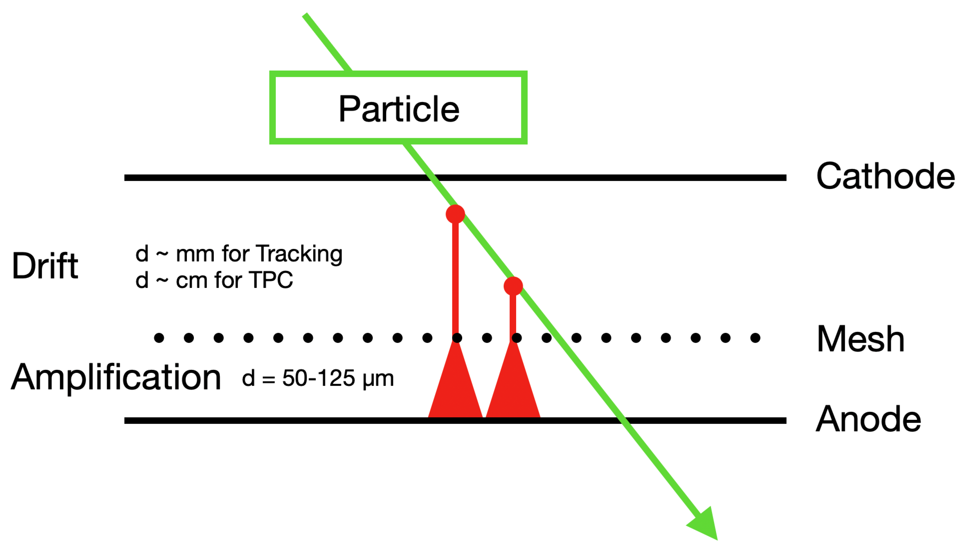
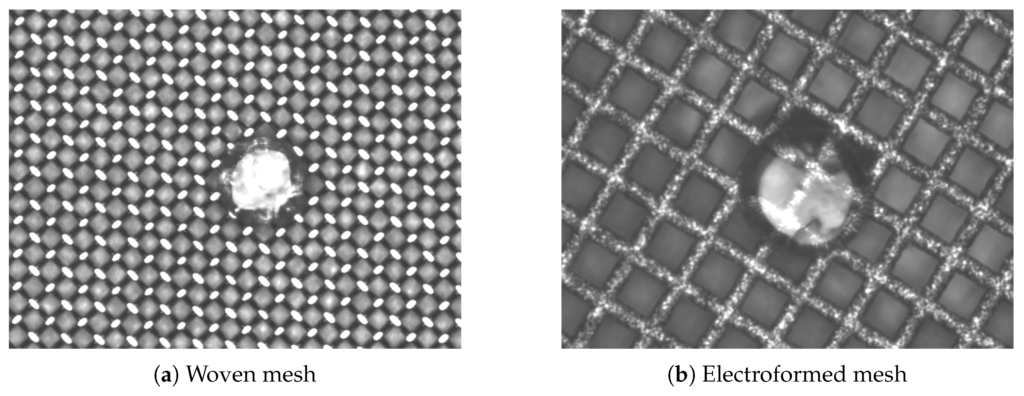
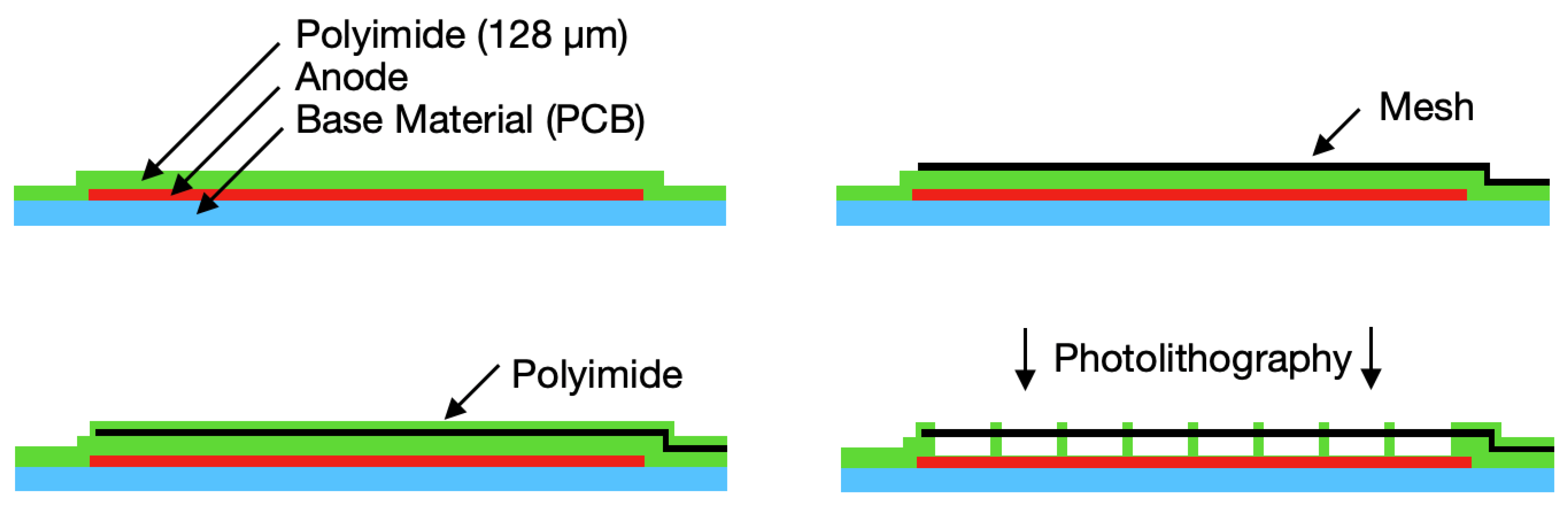
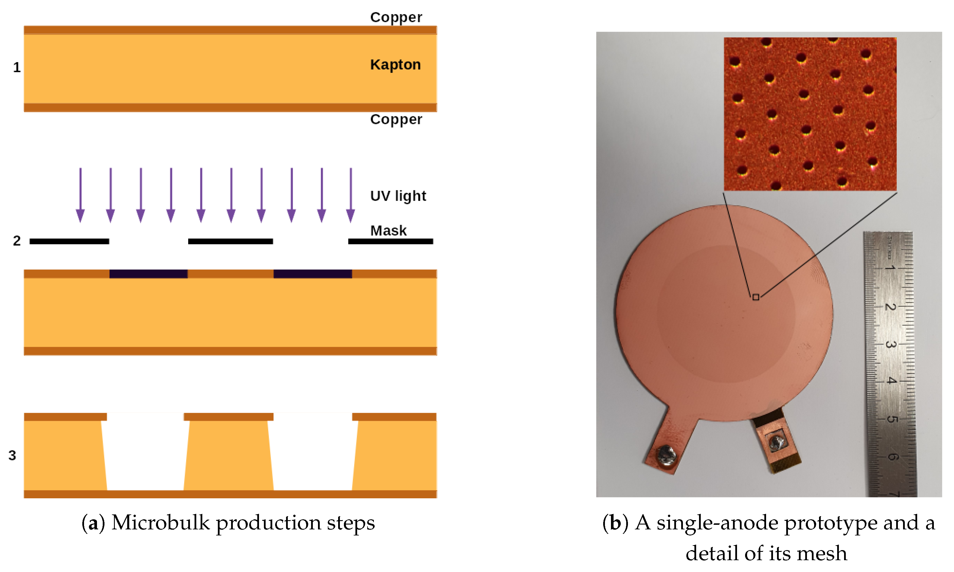
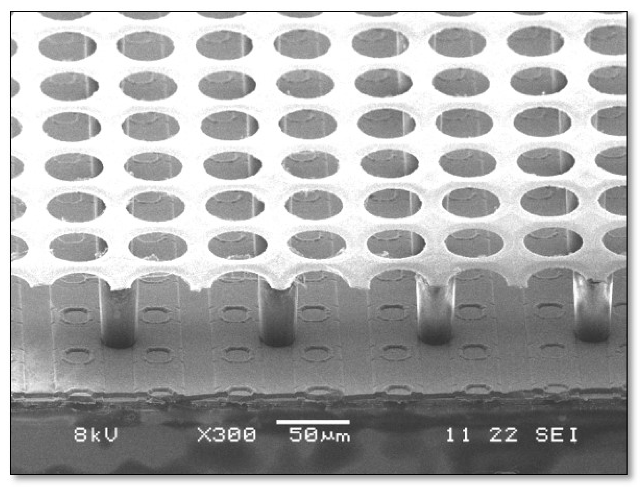
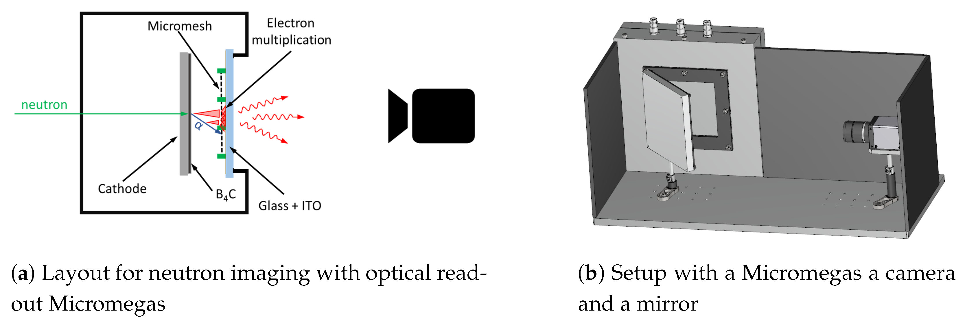
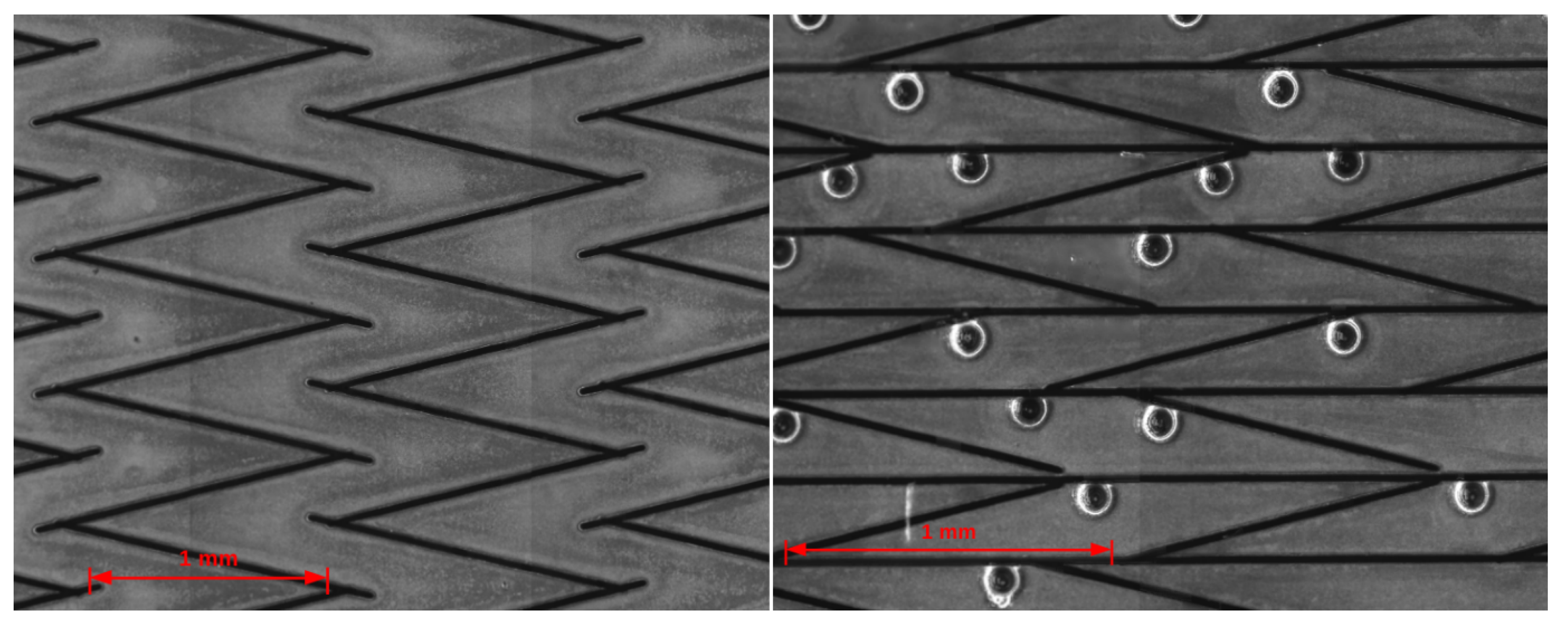
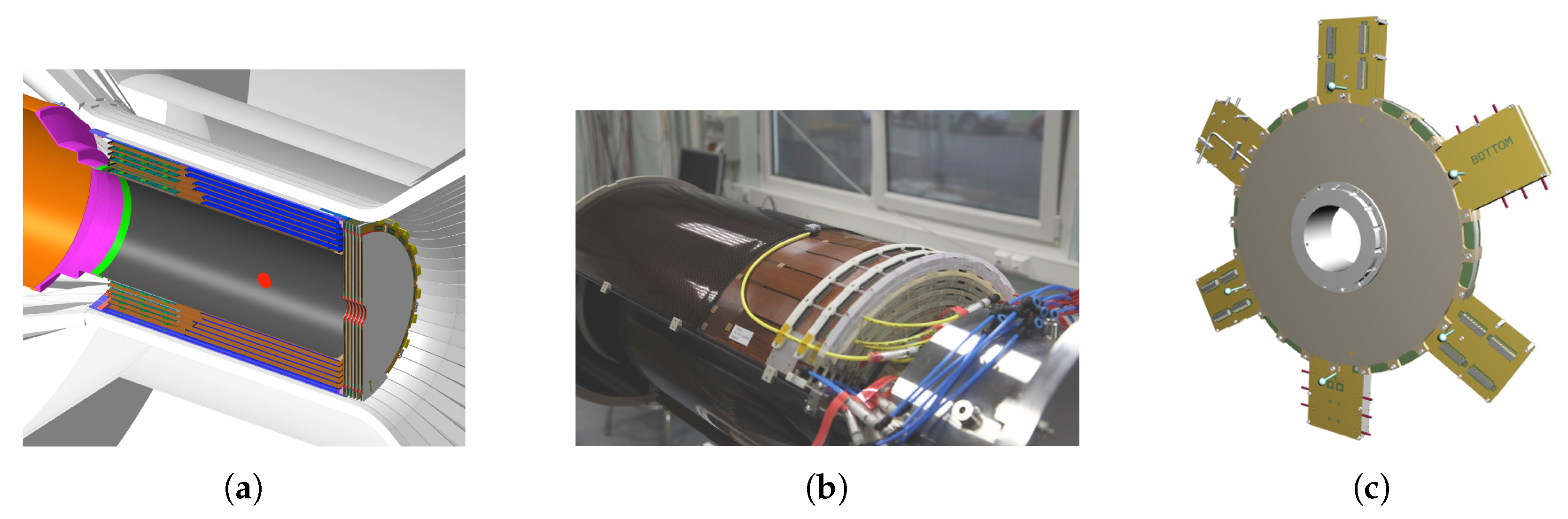
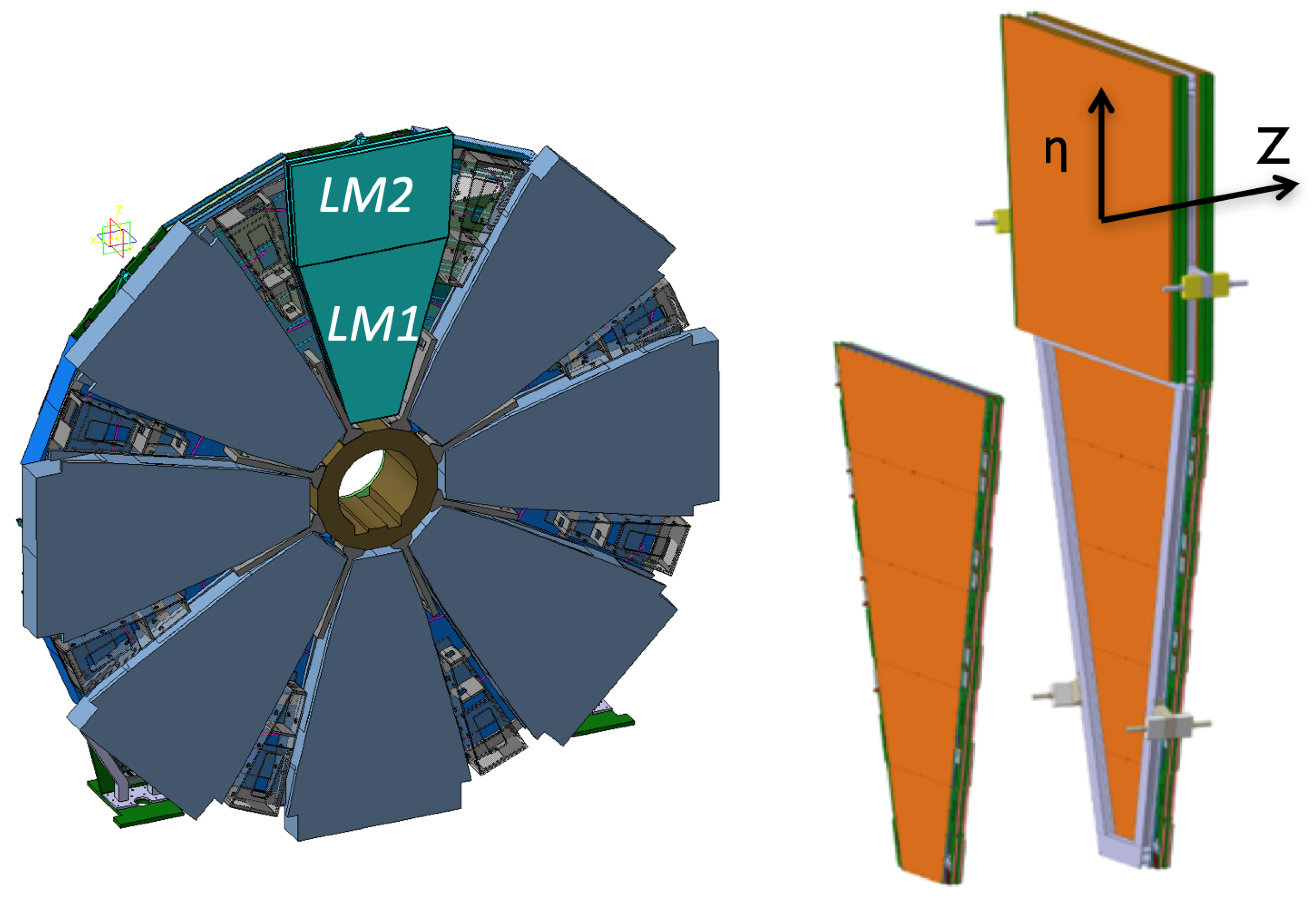
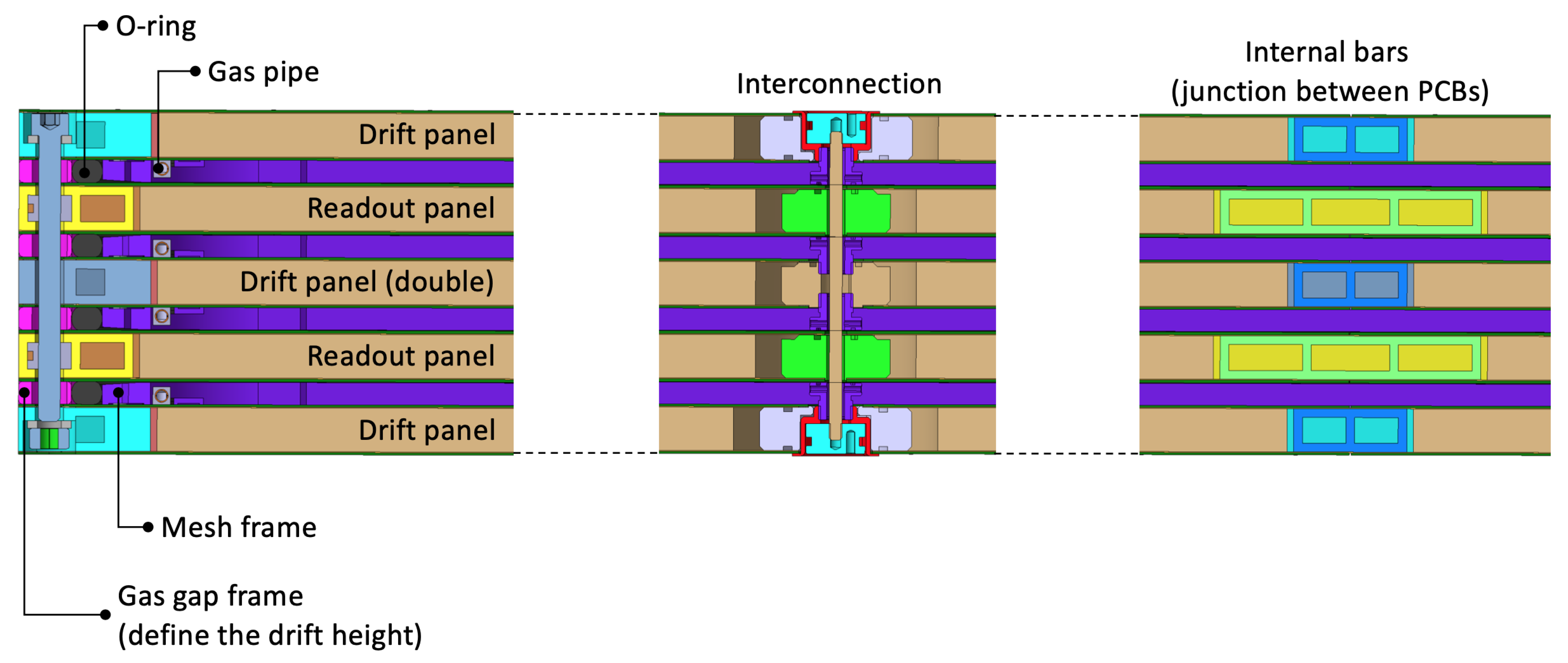
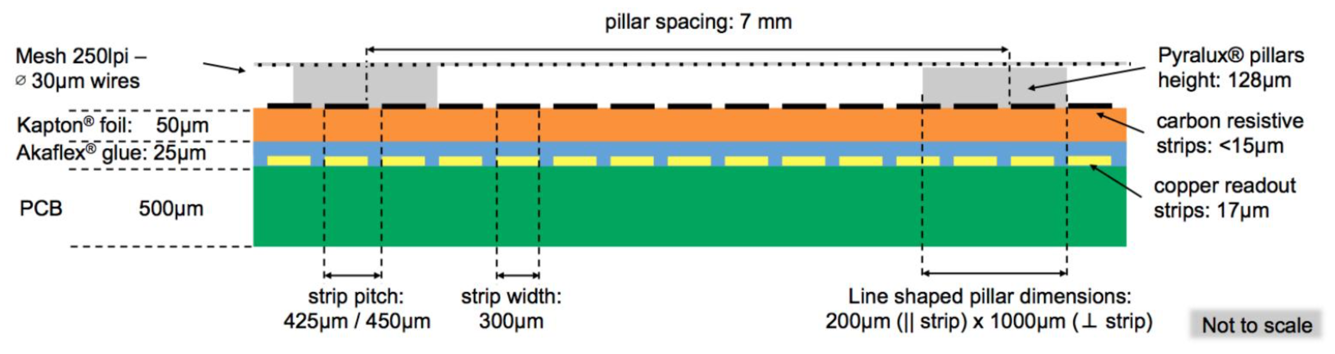
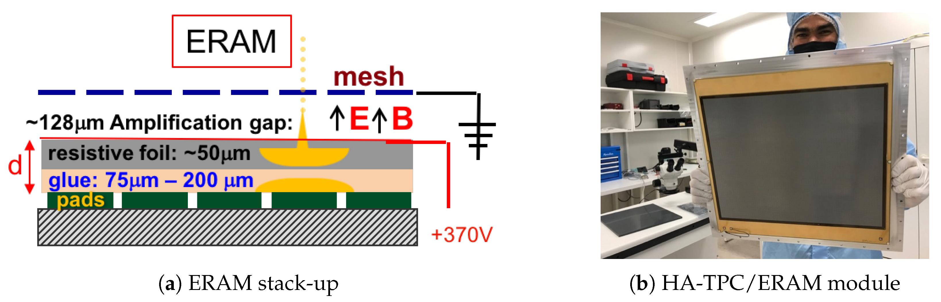
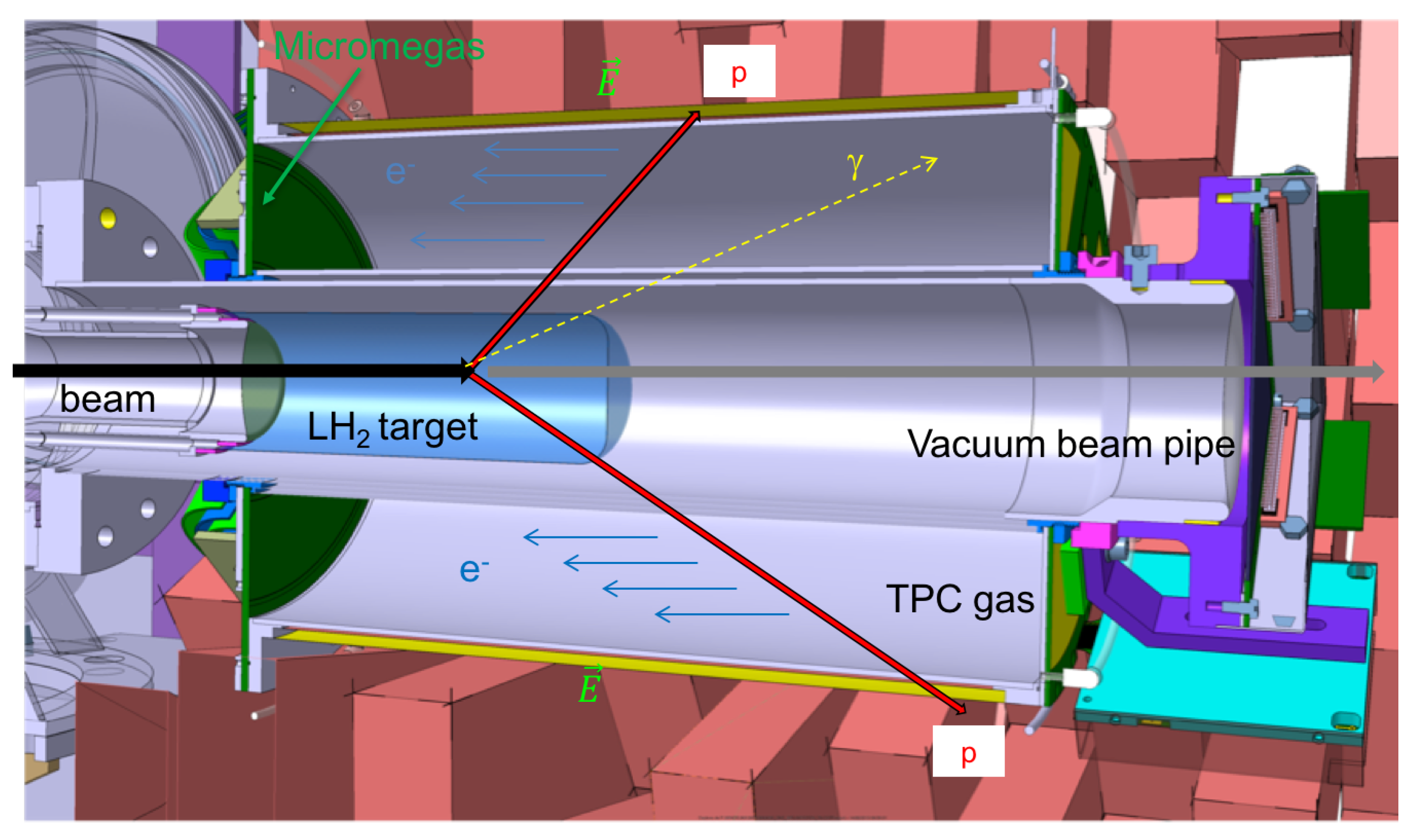
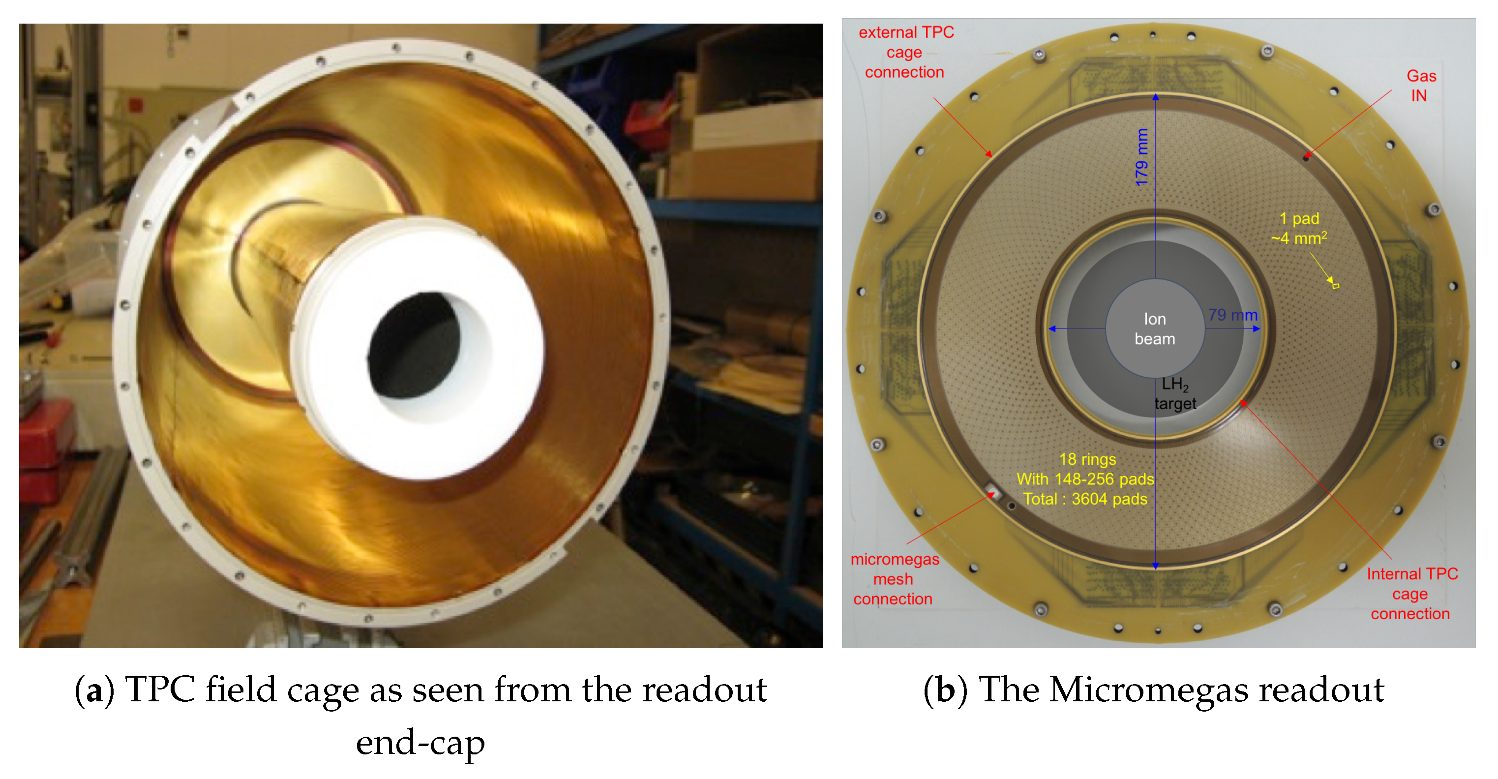
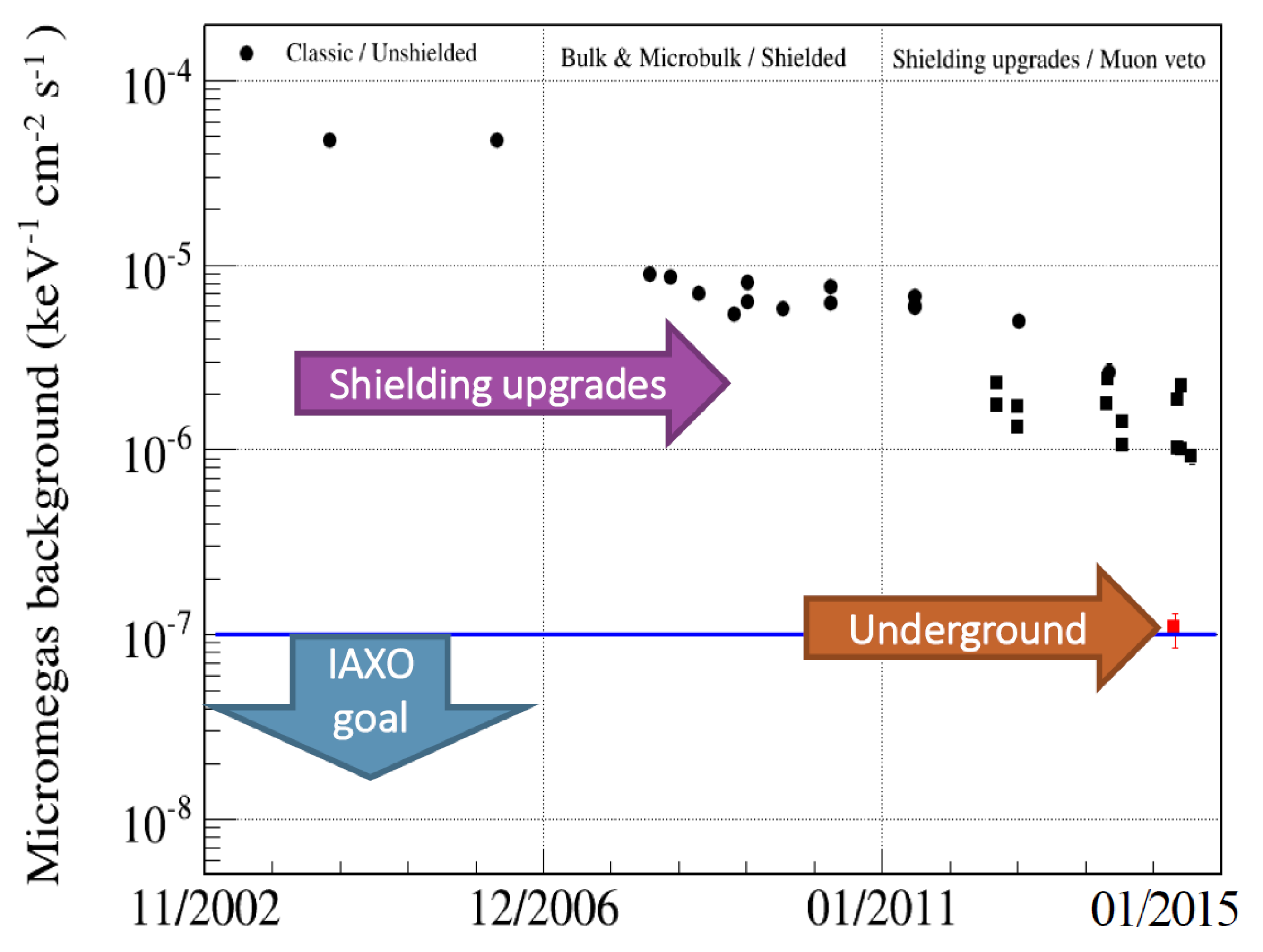
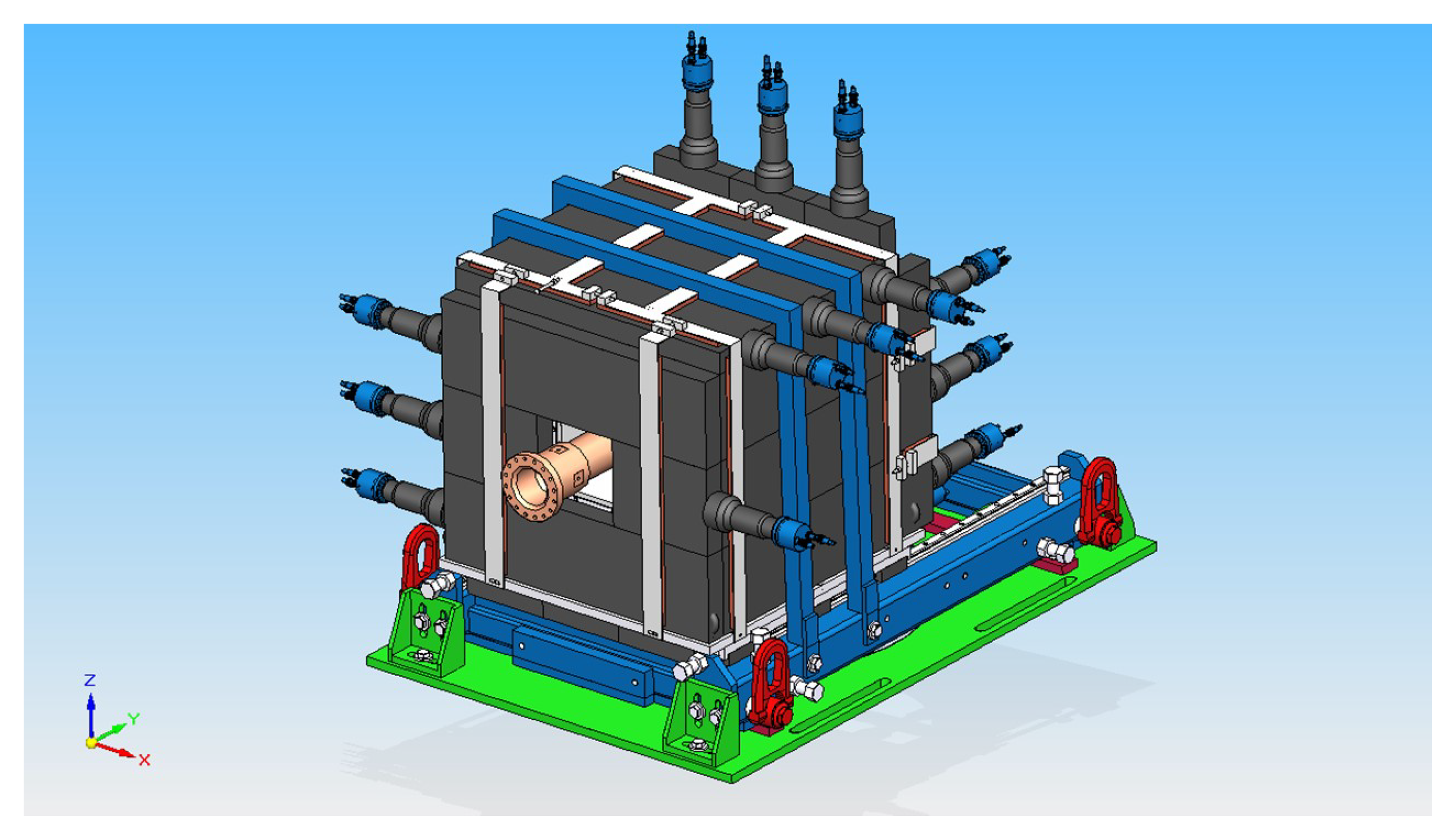
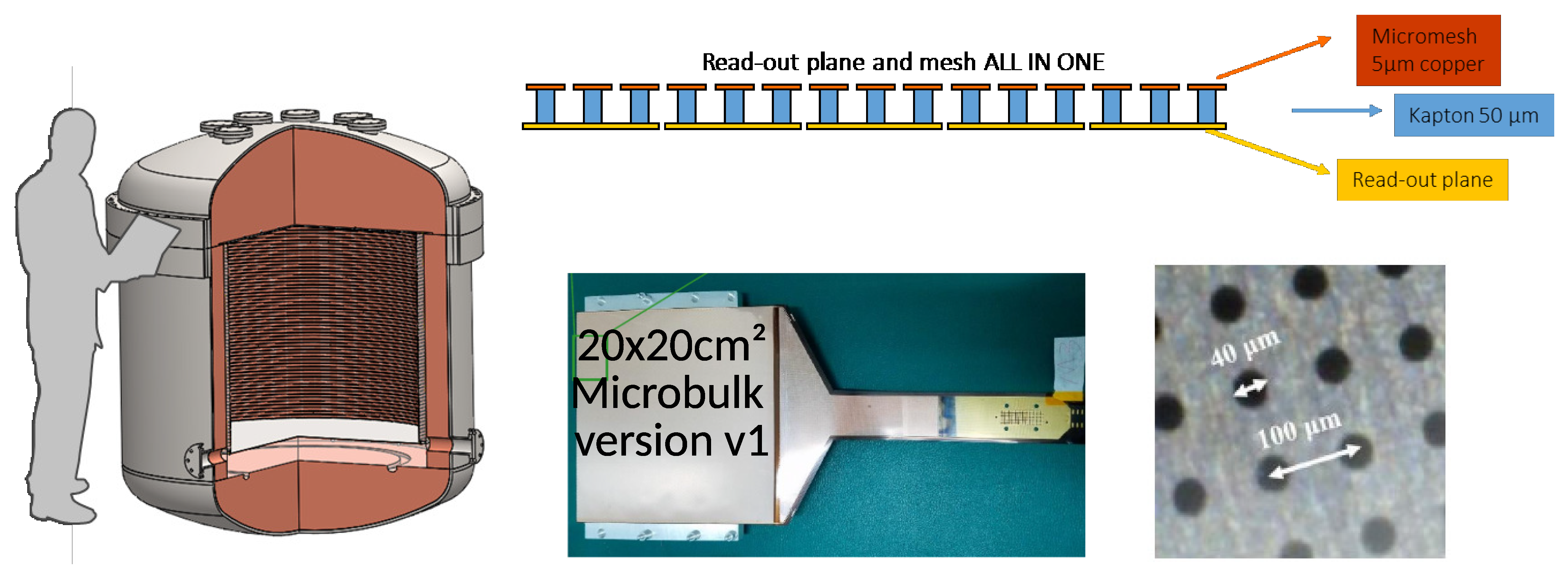
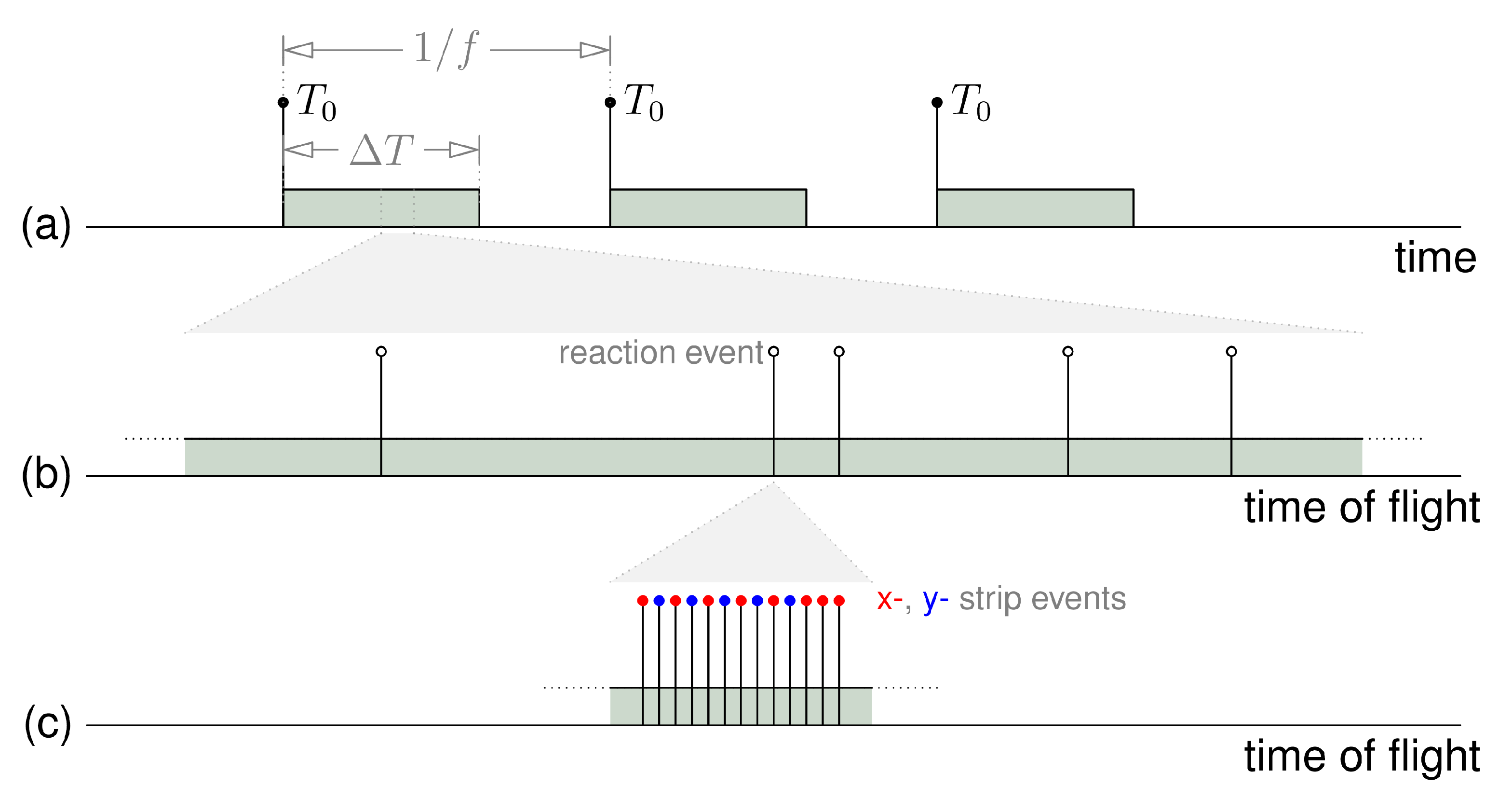
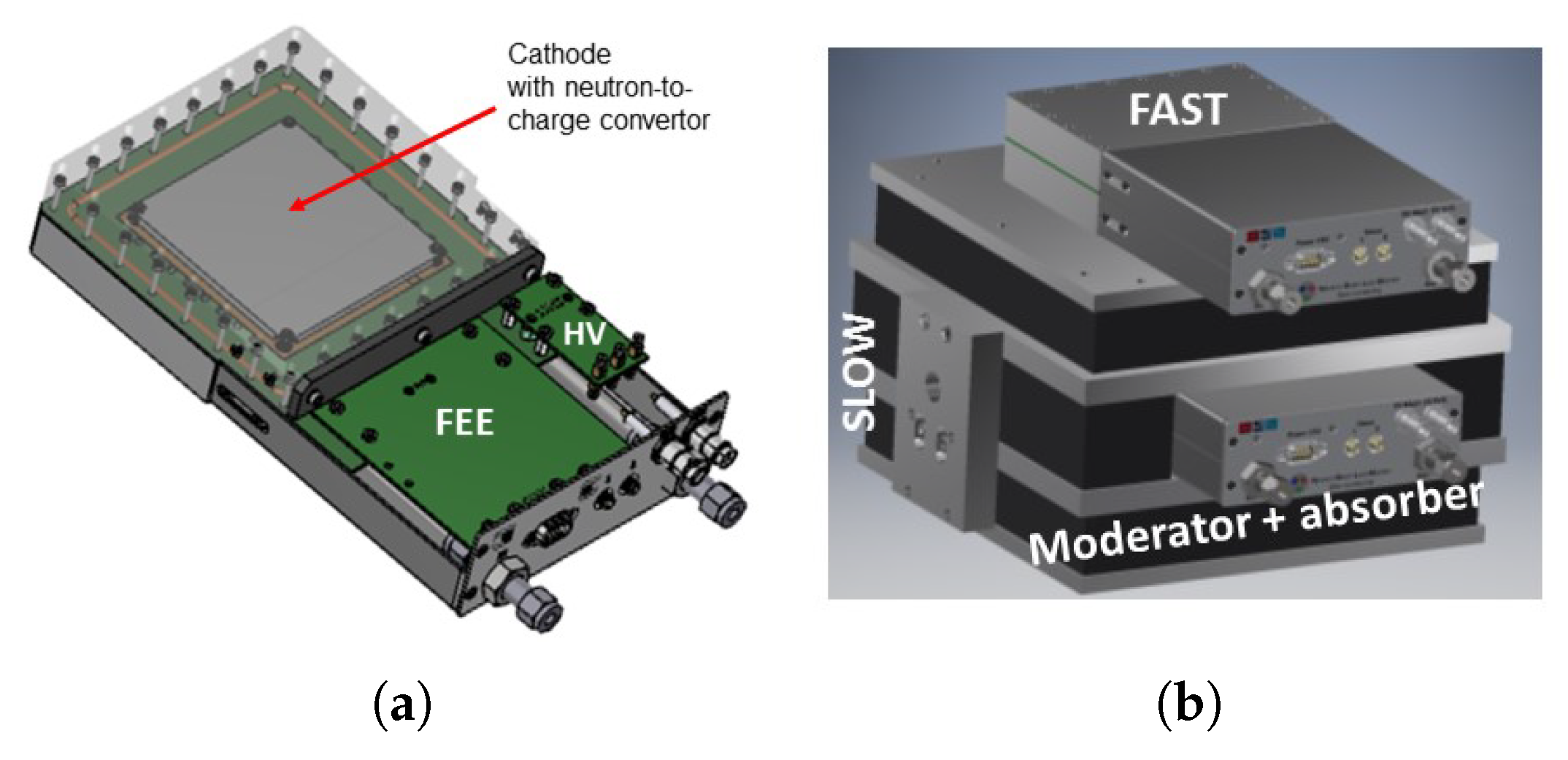
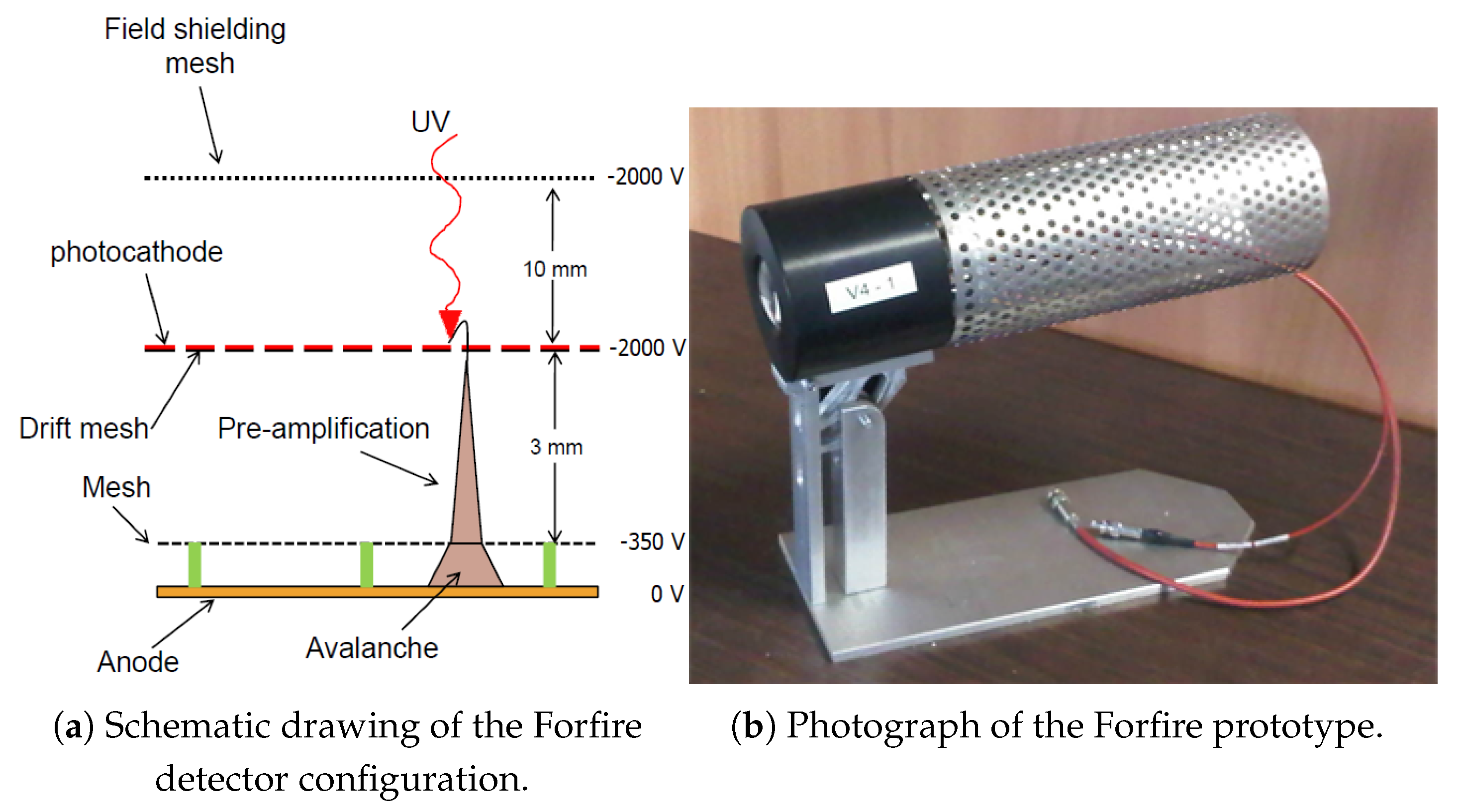
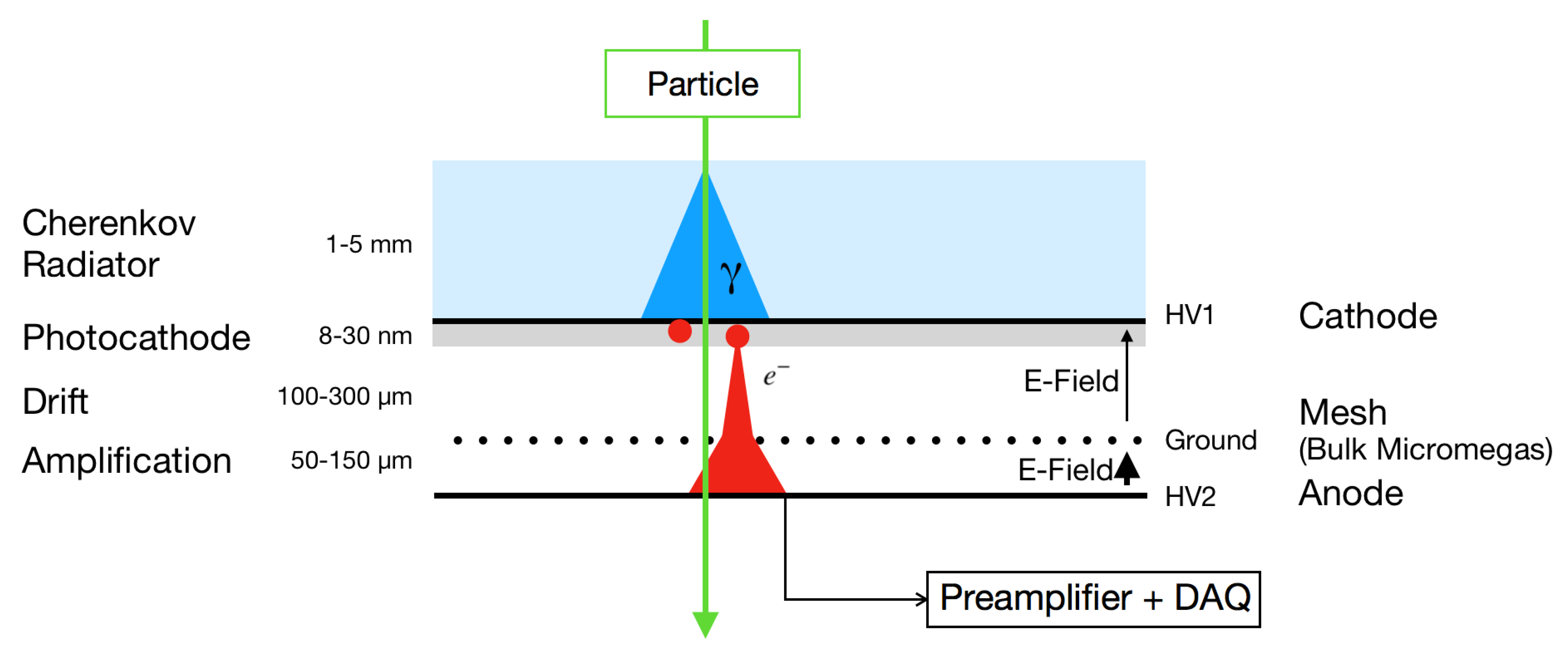