1. Introduction
With rapid progress in developing organic and inorganic materials, it becomes more important to determine the quality and performance of the manufactured products alongside with their reproducibility and repeatability in terms of characteristic parameters. These strongly depend on materials’ chemical composition, which often reveals itself directly in electromagnetic properties. The electromagnetic waves have been used for material characterization under various settings. Whereas the scanning microwave microscopy (SMM) techniques make it possible to quantitatively characterize, analyze, and categorize materials at microwave frequencies [
1,
2,
3,
4,
5,
6], in parallel, microwave resonator techniques are developed, which also focus on pure electromagnetic characterization at bulk level. The resonator based techniques also come with a much better ease-of-use and applicability in different industrial sectors. In particular, the split-post dielectric resonator (SPDR) has been accepted as a standard for characterizing low loss laminar dielectric materials accurately, conveniently, and in a non-destructive way [
7,
8,
9,
10].
This work constitutes a part of our research activities performed within the framework of the European Horizon 2020 MMAMA project [
11], which focuses on the development of various electromagnetic materials characterization techniques including SMM and dielectric resonator setups and their modelling. The modelling of SMM tips and generic dielectric resonators with low loss dielectric samples has already been reported [
5,
6], and an extension of dielectric resonator modelling to scanning setups has been presented in [
12]. In this paper, we focus on modelling and analyzing a real-life, industrially popular, and commercially available [
13] split-post dielectric resonator (SPDR). Its outstanding accuracy for microwave material measurements is acknowledged by the IEC norm [
14] and typically attributed to its rigorous design based on electromagnetic field expansion into Bessel functions [
7,
10], with the expansion coefficients obtained by dedicated solvers, assuming planar boundaries between the different materials. Our approach is to utilize the general-purpose finite-element (FEM) and finite-difference time-domain (FDTD) methods in cylindrical coordinates. We enforce zero angular dependence of the fields for the considered modes and conduct a numerical solution in the 2D long-section of the resonator. Hence, while the axial symmetry as in [
7,
10] is assumed, the boundaries between the materials do not need to be planar, allowing analysis of deformed samples. For the pure electromagnetic modelling of SPDR loaded with a dielectric sample, both FEM and FDTD are applied and quantitatively compared to the measurements. The measurement method and material parameters extraction are based on measuring changes in SPDR’s resonant frequency in case of an empty resonator and in the presence of sample under test (SUT). Then, theoretical analysis is conducted to investigate and understand behavior of semiconductor samples under different modes of the SPDR. A time-domain finite element method (TD-FEM) coupled multiphysics solver is adopted from [
15] and applied in order to model the nonlinear charge transport in semiconductor samples and to observe their effects in the resonance behavior. The focus has been on combining the two fields, that is, on reformulating the numerical algorithms for a computationally efficient solution of an industrially relevant problem of semiconductor measurements in popular SPDRs.
The paper is organized as follows.
Section 2 presents the geometry and materials of the SPDR and defines the modelling techniques used to perform eigenvalue analysis for dielectric samples. In
Section 3, simulation results have been given and verified with measurements of test samples in two SPDR units.
Section 4 describes the multiphysics analysis in order to account for measurement scenarios with homogeneously doped semiconductor samples.
Section 5 discusses the results and further steps required to improve the methods, and
Section 6 concludes the paper.
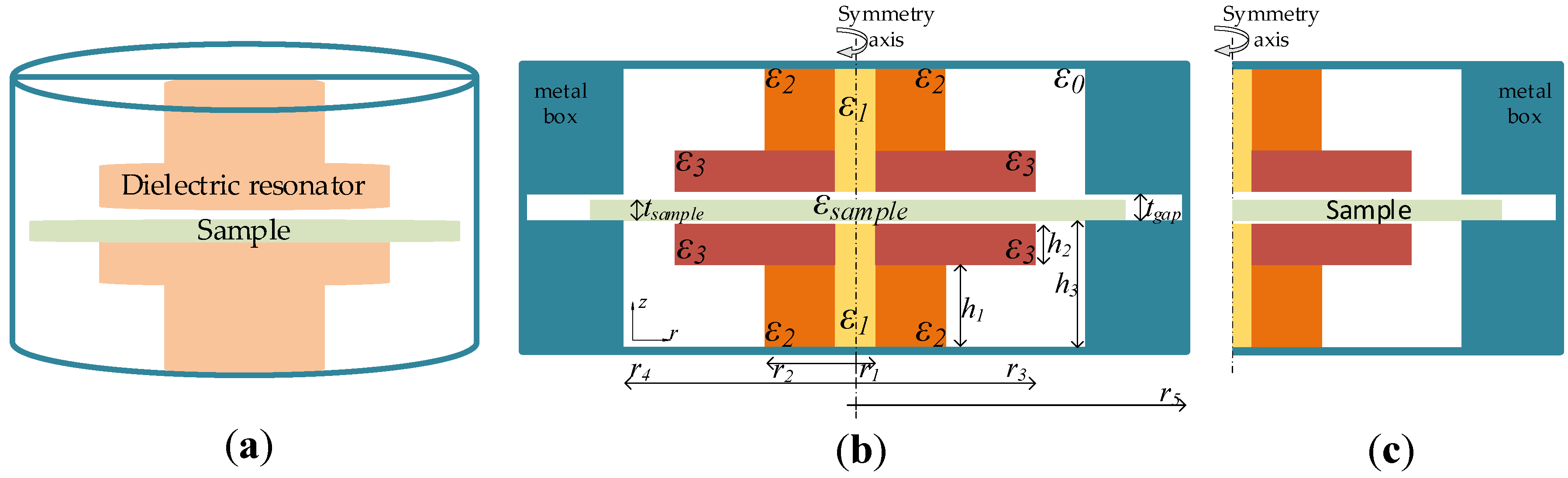
2. Eigenvalue Analysis of Dielectric Resonator
The electromagnetic analysis, aiming at determining resonant frequency of SPDR test-fixture, without and with dielectric sample inserted, has been conducted for the structure following [
9]. The SPDR is composed of two ceramic disks that are separated with a gap, supported with dielectric rods and surrounded with a metal enclosure. The benchmark is depicted in
Figure 1 and considered with relative permittivity values
and dimensions
. Such a resonator configuration has a nominal frequency of ca. 4.8 GHz. The conducted electromagnetic analysis benefits from axial symmetry of SPDR; therefore, the modelling scenario is reduced to the computational 2D problem. In the considered problem, the sample thickness is denoted by
and has relative electric permittivity
. Metallic enclosure outside the resonator is taken as perfect electric conductor (PEC) for the numerical purposes.
Firstly, a resource efficient vector 2D (V2D) formulation of the FDTD method for axisymmetric structures has been employed to extract the fundamental resonant frequency of the resonator without a sample (i.e., ). The aforementioned formulation allows for a problem size reduction by three orders of magnitude compared to standard 3D modelling, from 19,000,000 of FDTD cells and 1.8 GB of RAM memory occupation required for 3D model, to 17,000 of FDTD cells and 2 MB of RAM occupation for V2D. The computation of the resonant frequency takes ca. 30 s when run on nVidia GeForce GTX Titan.
For the same problem, an analogous axisymmetric formulation of frequency domain FEM (FD-FEM) [
5,
16] is also used to determine the fundamental frequency. Since it is physically known that the fundamental mode will only have
independent
component, the discretization is also done only for the
-component of E-field using scalar nodal shape functions. An in-house developed C + + solver is used with a mesh consisting of nearly 100,000 triangular elements, and it takes just under 2 s to determine the resonant frequency on an Intel-i7 processor, and it occupies 150 MB of RAM.
As expected, for a deterministic resonator problem, a frequency domain approach is capable of providing faster solutions than a time-domain approach. The obtained resonant frequencies with varying sample thicknesses and permittivities are given in the following section and verified with respect to own measurements performed for the purpose of this paper.
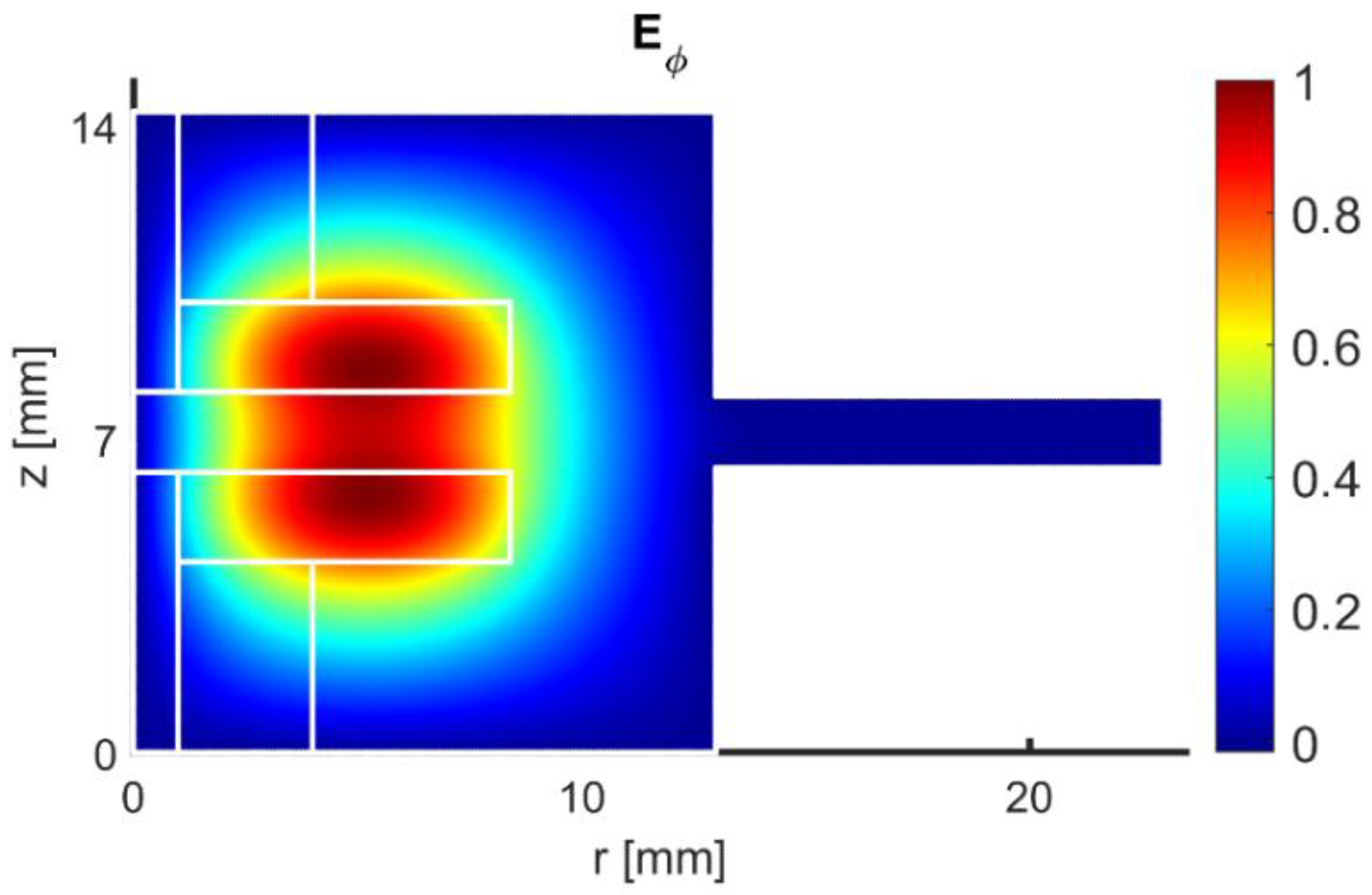
3. Results for SPDR with Dielectric Samples
Having defined the problem geometry and parameters, the next step was to determine resonant frequencies of the SPDR. Firstly, we have focused on the fundamental mode without any sample to cross verify and compare our FD-FEM and FDTD approaches. The E-field profile of the considered TE01
measurement mode at 4.95 GHz and its E-field profile is given in
Figure 2.
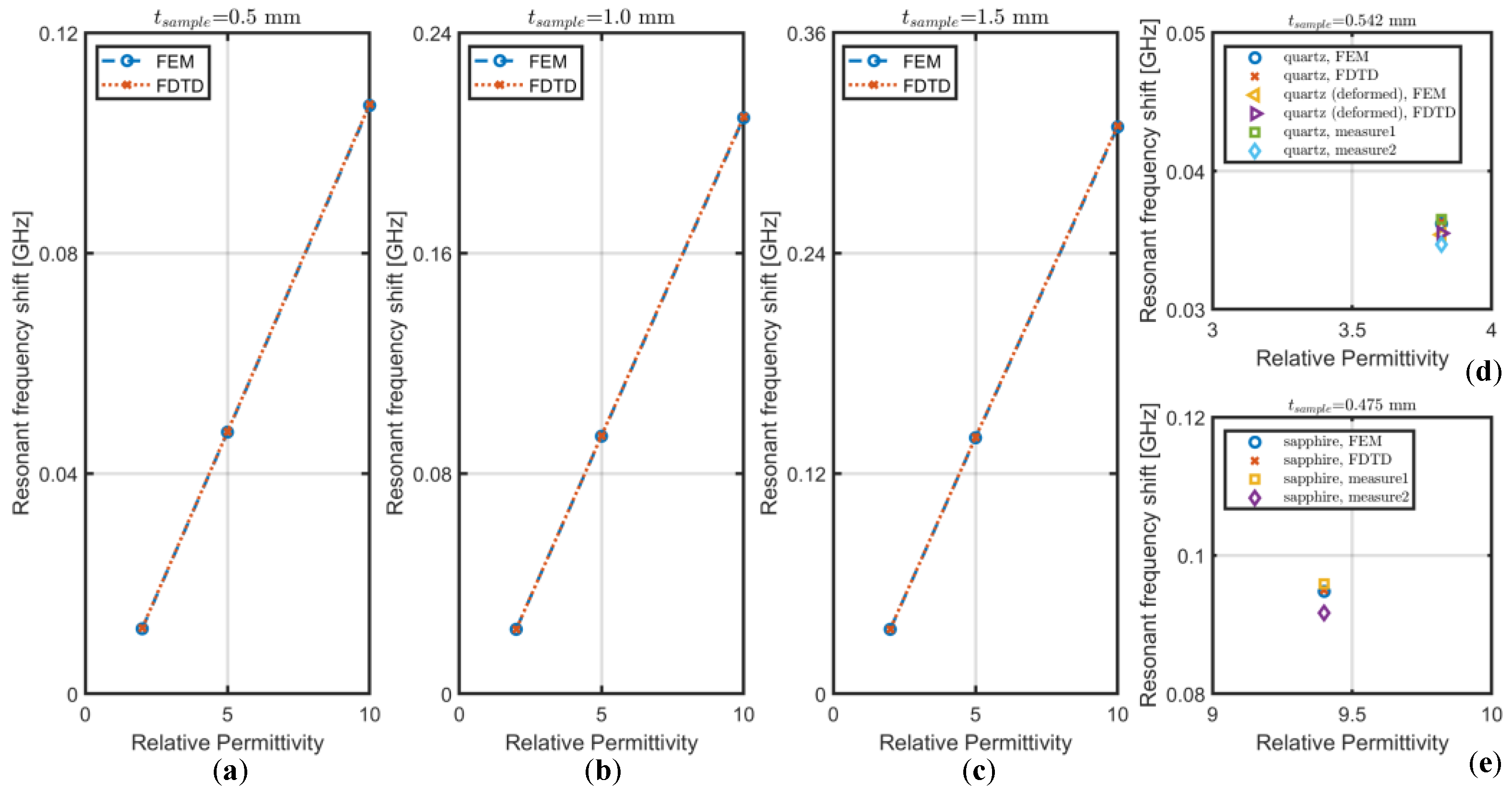
In addition to the no sample case, we have also obtained several resonant frequencies for different sample thicknesses and different sample permittivities, including analysis of real-life material samples, namely quartz (
) and sapphire (
). Additionally, a non-planar (cone-shaped) sample (to represent realistic deformation), which is not perfectly horizontal in the sample slot but bent upwards in the middle, is considered. The results of performed calculations are given in the
Table 1, and the discrepancies in the resonant frequency extraction between the two simulation methods do not exceed 4.2 MHz.
The comparison of simulated and measured frequency values reveals the differences of ca. 200 MHz. The observed higher difference is understandable, as the physical device may differ from its design due to being a subject to manufacturing modifications and tolerances, making each unit unique in terms of geometry and resulting resonant frequency, which is confirmed with two different resonant frequencies obtained for the two adopted commercial units (
Table 1).
The extraction method for permittivity is based on measuring the shifts in the resonant frequency of an empty and sample-loaded SPDR; therefore, the frequency shift (and not the frequency itself) directly determines the permittivity value. These frequency shifts have been calculated for the considered simulation scenarios and experiments, and results have been visualized in
Figure 3.
The obtained values of the frequency shifts are consistent between FDTD and FEM simulations performed for arbitrary samples’ thicknesses and permittivities, not exceeding 0.5 MHz reported for thick high-permittivity samples. Similar observation is made for frequency shifts under the presence of real material samples of quartz and sapphire, obtained from EM simulations and measurements, proving applicability of both FDTD and FD-FEM methods in their formulation dedicated to axisymmetric structures, to accurate analysis and design of dielectric resonator-based test-fixtures for material characterization.
4. Multiphysics Analysis for SPDR with Semiconductor Samples
SPDR have already been used for semiconductor (SC) characterization as in [
9]; however, modelling of such measurement scenarios were always limited to bulk semiconductor parameters. In this section, we analyze such a scenario by taking semiconductor physics into account as well, so that the local conductivity changes due to charge movements are also considered. The charge transport in semiconductors can be modelled with the well-known drift-diffusion equations. These transport equations are usually solved together with Poisson equation to give a complete picture of the charges in semiconductor regions [
17]:
where
is the electric potential,
is the electron (hole) concentration,
is the net generation-recombination rate of carriers,
is the electron (hole) current density,
and
are the ionized donor and acceptor charge densities due to doping,
(
is the electron (hole) mobility (
and
respectively),
is the electron (hole) diffusion coefficient (
and
respectively),
is the electric permittivity of semiconductor material respectively, and
(
) is the elementary charge. Equation (1) is the Poisson equation for electric potential; (2) and (3) are the continuity equations for the charge carriers. This set of equations is supplemented by carrier transport Equations (4) and (5), which take both drift and diffusion of charges into account. For the net generation–recombination rate of the charges, the widely used Read–Hall–Shockley recombination mechanism (
), where average life times for the carriers are taken as
, and
is the intrinsic carrier concentration), is assumed. This set of Equations (1)–(5) is valid when the semiconductors are modelled themselves without external E-field (
) illumination, if they are also illuminated through external field, the transport equations take the following form:
Hence, the transport is not only affected due to curl-free internal built-in potential, but also divergence free wave part of the E-field. In addition, the movement of the carriers (depletion and accumulation) creates position dependent conductivity as , which will be taken into account by the electromagnetic solver, affecting the resonance.
We initially considered the scenario where a homogeneously doped silicon wafer is inserted into our SPDR. For the fundamental mode that has been used to characterize materials in the previous Section, it is known that the external E field will have the form , which will cause azimuthal closed loop current flow on the silicon sample. Therefore, there is not any local carrier distribution in the r–z plane of the axisymmetric structure, and no change in resonance frequency will be observed.
However, if we consider a higher order mode, which has electric field in the form of , it is expected to observe effects due to local conductivity changes that occur when the mode is present.
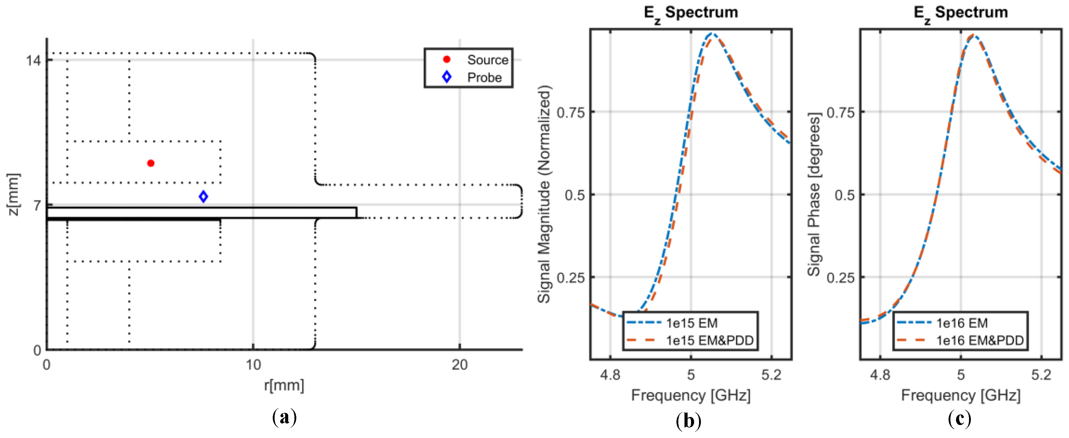
In order to be able to couple electromagnetics solver with highly nonlinear semiconductor physics, we have employed time–domain (TD) FEM, as it offers flexible capabilities for multiphysics modelling. We have first developed a TD-FEM electromagnetic solver in which a point source and a few probing locations are defined. After exciting with a Gaussian burst time-domain signal centered at 5 GHz, and taking the Fourier Transform of the time-domain signals observed at different probing locations, we were able to distinguish the modes supported by the structure. The resonance frequencies have been determined by analyzing field spectrum at the probe locations, and in all the cases, these peaks in the spectrum were clearly distinguishable and the maxima points correspond to the resonance frequencies. Additionally, the spectrum obtained from the probe locations show clear frequency shifts with respect to the source spectrum, providing information regarding the resonant behavior of the structure. The first higher mode (named as TM01) with independent and components, without any sample is observed at 5.33 GHz, and the FDTD solver also verifies the existence of the same mode at 5.31 GHz.
Verification of our coupled electromagnetic (EM) and Poisson–Drift–Diffusion (PDD) algorithm and solver was performed with the aid of TD-FEM electromagnetic analysis performed for material samples characterized also with bulk conductivity values.
Table 2 gathers the values of TM01
frequencies obtained from simulations conducted for different material sample parameters and solvers’ configurations.
Traditional semiconductor simulation tools employ the Poisson equation together with the transport equations for the modelling of semiconductor devices. For the high frequency excitation where the wavelength becomes as small as device dimensions, the Poisson equation is replaced with the Maxwell’s equations, as in [
18], to be computed with the transport equations. Replacing Poisson’s equation also means that the traditional potential-based boundary conditions would have to be changed, making it challenging to apply classical semiconductor boundary conditions, i.e., ohmic, Schottky, etc. In [
15], another method is developed to simulate the semiconductor devices where the Poisson equation is also solved in addition to the wave equation. This method provides flexible semiconductor modeling, making it possible to use terminal potentials for the semiconductor boundary conditions (AC or DC excitation) together with external electromagnetic illumination. Additionally, this method ensures the full coupling of the divergence-free electric field that is the outcome of the wave equation and curl-free electric field component that is coming from the Poisson equation for the charges as in the Equations (5) and (6). Unlike the popular commercial tools where the drift diffusion equations only include the curl-free part of the electric field, the proposed method contribution of both electric field components (divergence-free and curl-free) are taken into account for the calculation of the semiconductor current equations. Consequently, the position dependent electrical conductivity used in the wave equation is updated at every time step using the local charge distribution obtained from the modified carrier transport.
Among the previously reported algorithms [
15,
18], the coupled multiphysics FEM based algorithm described in [
15] is adopted to simulate SPDR. The scenario with homogeneously doped silicon sample has been tested with the time-domain coupled solver with 200,000 time steps of size 0.5 ps in order to simulate a time-domain Gaussian burst, and the signals analyzed at probing locations. The frequency spectrum with resolution of 10 MHz is obtained from the observed waveforms, and the peak locations show the resonant frequencies. In
Figure 4, the spectrum comparison between the bulk conductivity case (EM solver only) and the multiphysics case (EM - PDD) for two different n-type doping levels, 10
15 cm
−3 and 10
16 cm
−3, is presented. As the doping of the semiconductor increases, its electrical conductivity also increases, and the sample starts to show behavior that is more
metallic. For the highly conductive samples, it is observed that the EM-PDD coupled solver predicts resonant frequencies very close to the ones that are obtained by the EM solver with the bulk parameters. For shallow doping, however, the nonlinear effects of the semiconductor domain might shift the resonance slightly. This change can also be observed in
Figure 4b for n-type doping of 10
15 cm
−3.
5. Discussion of the Modelling of SPDR Loaded with Semiconductor Samples
It is possible to claim the effects due to nonlinearities of the semiconductors on the resonant peak are minimal for the homogeneously doped silicon wafer. However, this developed coupled solver would also enable us to simulate non-homogeneous doping on the wafer (possible junctions, devices, etc.). In order to improve the resolution of TD-FEM based solvers, one can run even longer simulations that might require more computational power.
For the accurate simulation of the SPDR with semiconductor samples, it is important to consider the possible effects due to nonlinearities of the semiconductors, and one needs to consider PDD equations set for accurate modelling. Especially for the lower conductivity of the samples, the effects due to nonlinear nature of the semiconductors start to affect the analysis. These effects are still not so big, and one could avoid costly EM-PDD coupled simulations if the doping of the semiconductor sample is homogeneous. However, if the doping changes from region to region, in order to be able to model the depletion regions that are formed between the junctions of different doping levels, it is mandatory to employ a PDD solver. Here in this work, our focus was to analyze the possible effects of the semiconductor samples with homogeneous doping, and it is shown that for the fundamental mode with the -oriented electric field fundamental mode, the semiconductor can easily be modelled without the coupled solver as a bulk lossy dielectric, and for the higher order modes with r- and z-oriented electric field components, one should be careful about the doping of the sample, and the physical model can be chosen based on the required accuracy of the simulation.

 ,
, 


