Nanoporous Anodic Alumina Photonic Crystals for Optical Chemo- and Biosensing: Fundamentals, Advances, and Perspectives

 ,
,
Abstract
:1. Introduction
2. Fabrication and Properties: Nanoporous Anodic Alumina as Effective Medium
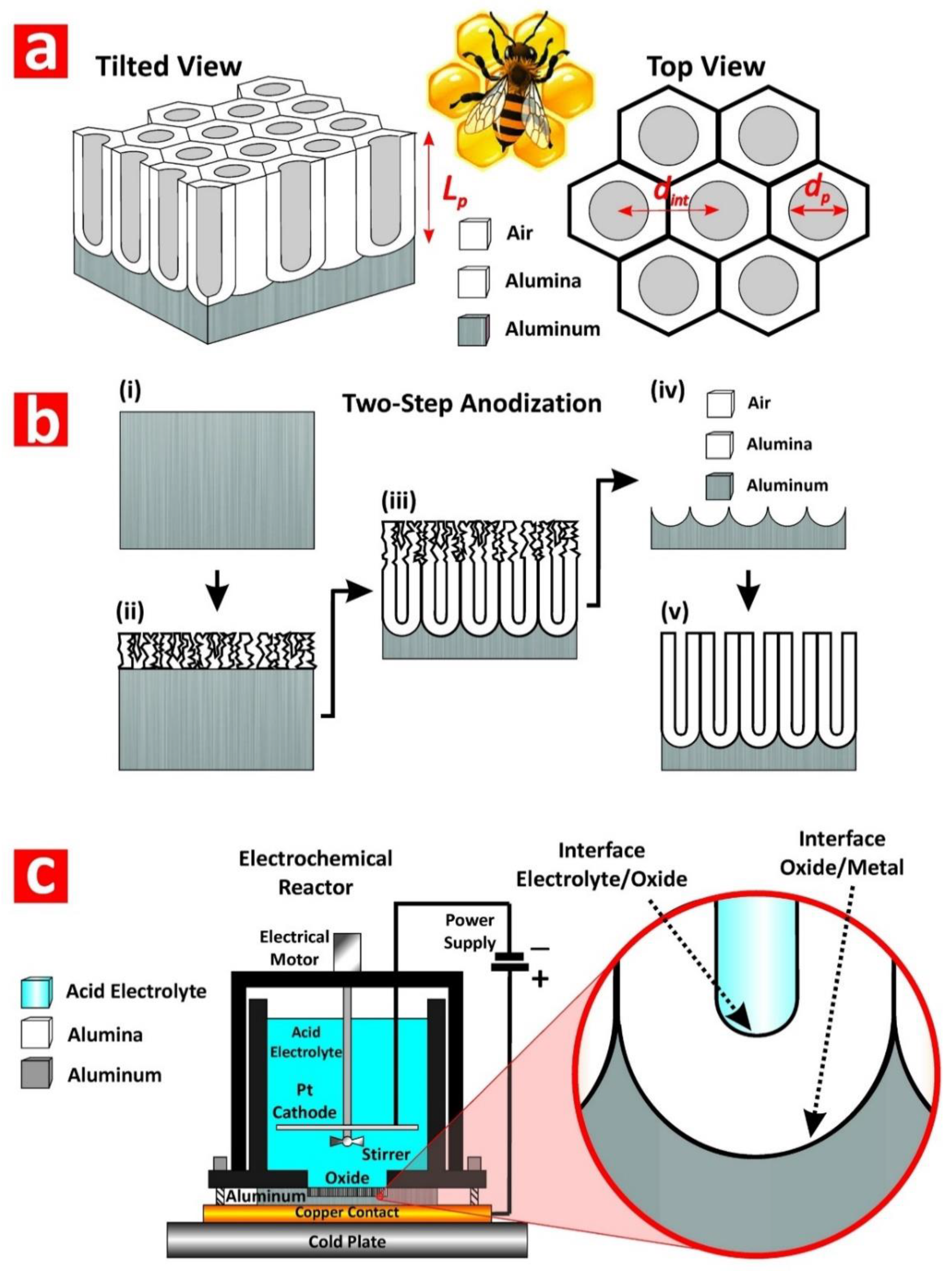
2.1. Fabrication of Self-Organized Nanoporous Anodic Alumina
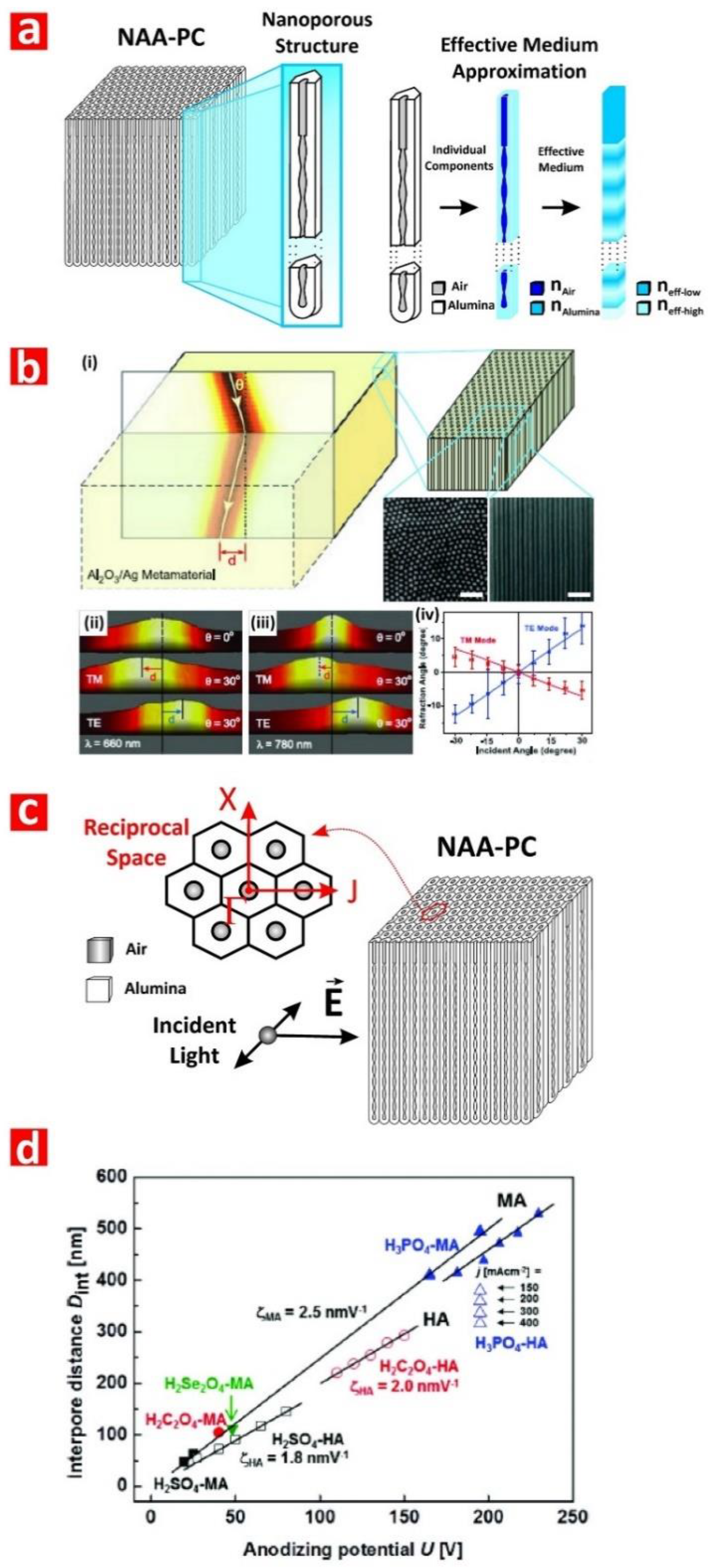
2.2. Physical Properties of Nanoporous Anodic Alumina
2.3. Structural Engineering of Nanoporous Anodic Alumina
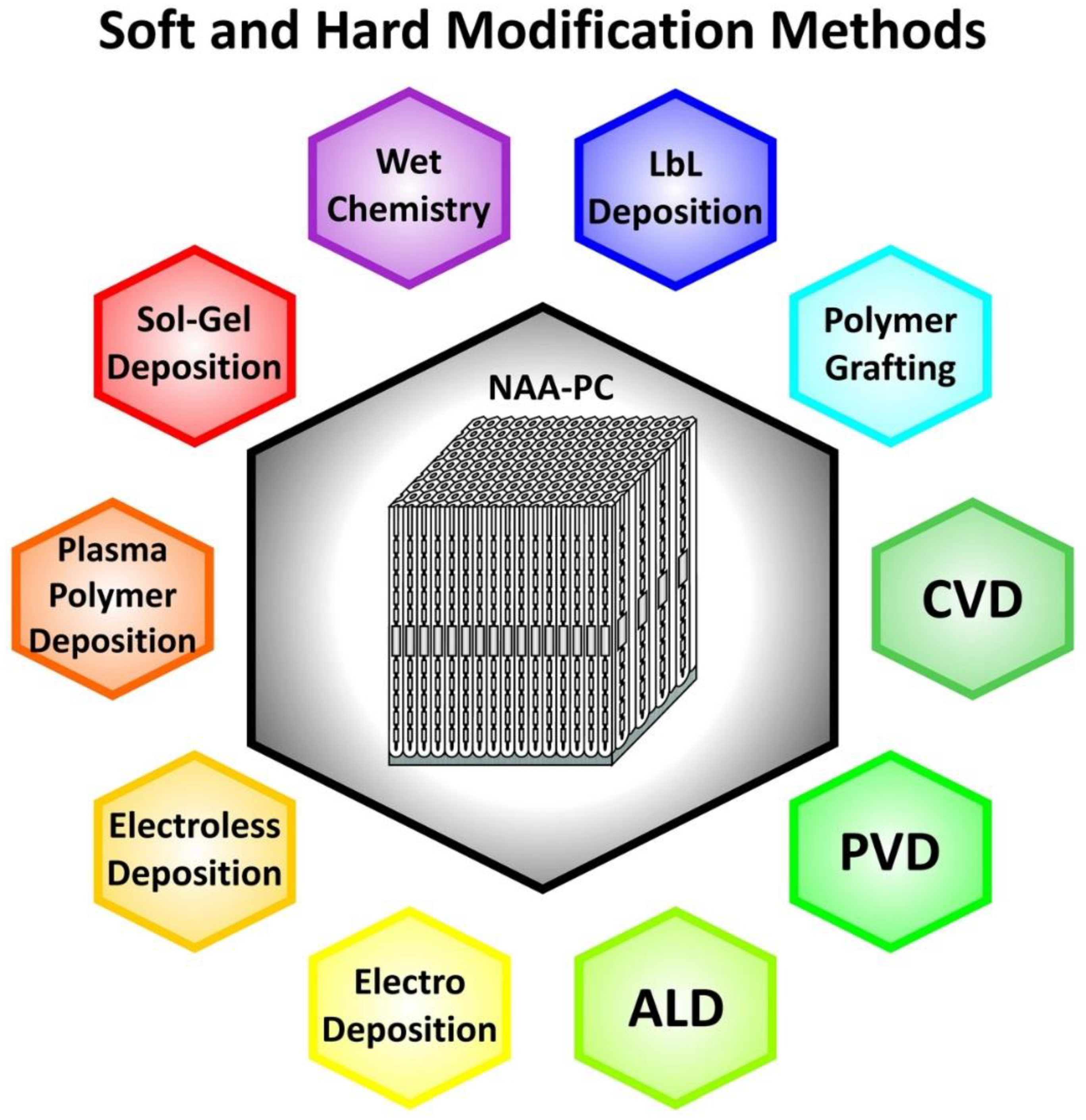
3. Surface Modification of Nanoporous Anodic Alumina Photonic Crystals
3.1. Soft Chemical Modification Techniques
3.1.1. Wet Chemistry
3.1.2. Layer by Layer Deposition
3.1.3. Polymer Grafting
3.2. Hard Chemical Modification Techniques
3.2.1. Chemical Vapor Deposition
3.2.2. Physical Vapor Deposition
3.2.3. Atomic Layer Deposition
3.2.4. Electrochemical Deposition
3.2.5. Electroless Deposition
3.2.6. Plasma Polymer Deposition
3.2.7. Sol-Gel Chemistry Deposition
4. Nanoporous Anodic Alumina Photonic Crystals as Optical Sensing Platforms
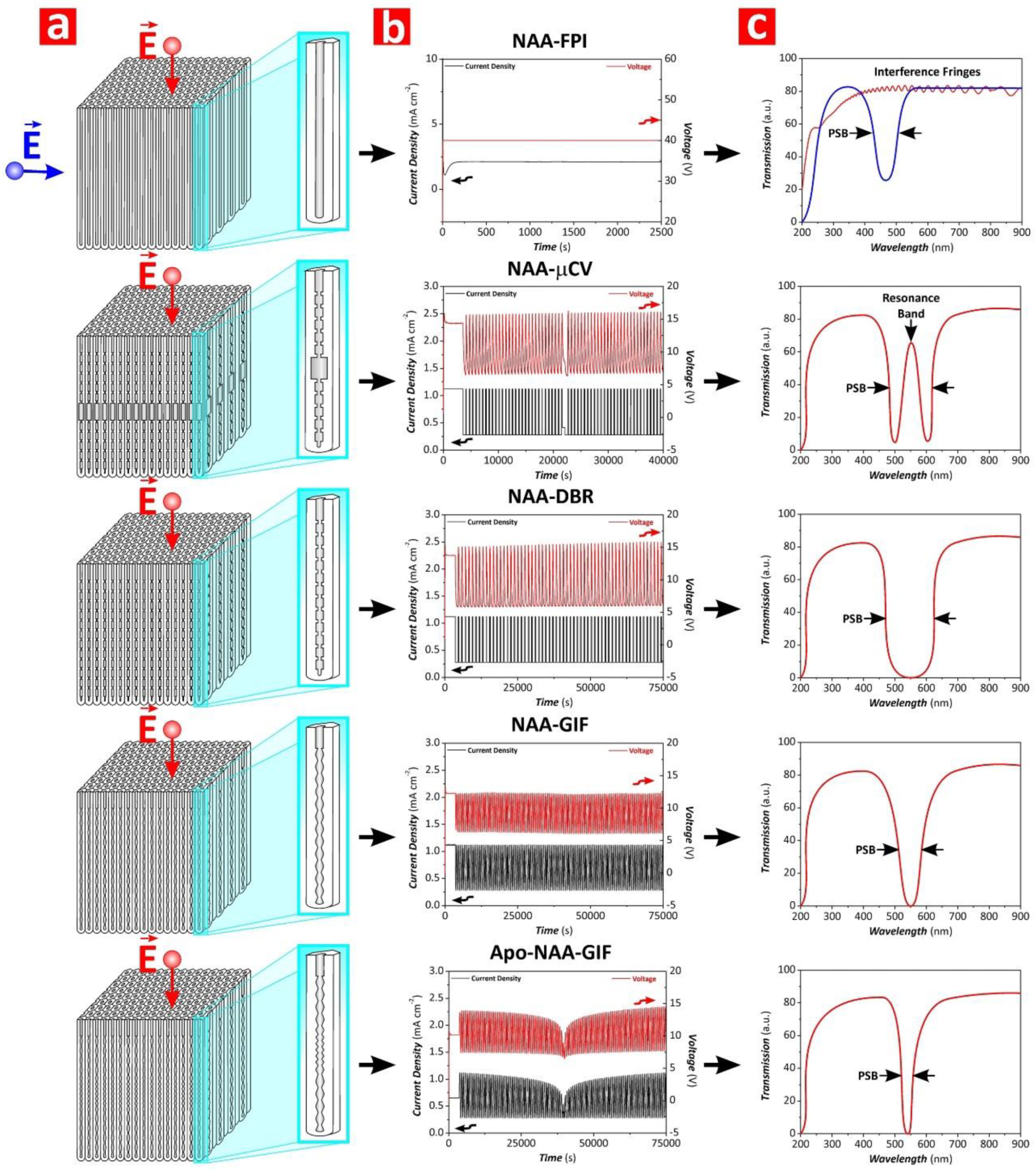
4.1. Nanoporous Anodic Alumina Distributed Bragg Reflectors (NAA-DBRs)
4.2. Nanoporous Anodic Alumina Gradient-Index Filters (NAA-GIFs)
4.3. Nanoporous Anodic Alumina Optical Microcavities (NAA-μCVs)
4.4. Nanoporous Anodic Alumina Fabry–Pérot Interferometers (NAA-FPIs)
4.5. Other Nanoporous Anodic Alumina Photonic Crystal Sensing Platforms
5. Conclusions
Funding
Acknowledgments
Conflicts of Interest
References
- Homola, J.; Yee, S.S.; Gauglitz, G. Surface plasmon resonance sensors: Review. Sens. Actuators B Chem. 1999, 54, 3–15. [Google Scholar] [CrossRef]
- Holtz, J.H.; Asher, S.A. Polymerized colloidal crystal hydrogel films as intelligent chemical sensing materials. Nature 1997, 389, 829–832. [Google Scholar] [CrossRef]
- Dickinson, T.A.; White, J.; Kauer, J.S.; Walt, D.R. A chemical-detecting system based on a cross-reactive optical sensor array. Nature 1996, 382, 697–700. [Google Scholar] [CrossRef] [PubMed]
- Rosenstein, J.K.; Wanunu, M.; Merchant, C.A.; Drndic, M.; Shepard, K.L. Integrated nanopore sensing platform with sub-microsecond temporal resolution. Nat. Methods 2012, 9, 487–492. [Google Scholar] [CrossRef] [PubMed] [Green Version]
- Miles, B.N.; Ivanov, A.P.; Wilson, K.A.; Dogan, F.; Japrung, D.; Edel, J.B. Single molecule sensing with solid-state nanopores: Novel materials, methods, and applications. Chem. Soc. Rev. 2013, 42, 15–28. [Google Scholar] [CrossRef] [PubMed]
- Hotta, K.; Yamaguchi, A.; Teramae, N. Nanoporous waveguide sensor with optimized nanoarchitectures for highly sensitive label-free biosensing. ACS Nano 2012, 6, 1541–1547. [Google Scholar] [CrossRef] [PubMed]
- Dhathathreyan, A. Real-time monitoring of invertase activity immobilized in nanoporous aluminum oxide. J. Phys. Chem. B 2011, 115, 6678–6682. [Google Scholar] [CrossRef] [PubMed]
- Yeom, S.H.; Kim, O.G.; Kang, B.H.; Kim, K.J.; Yuan, H.; Kwon, D.H.; Kim, H.R.; Kang, S.W. Highly sensitive nano-porous lattice biosensor based on localized surface plasmon resonance and interference. Opt. Express 2011, 19, 22882–22891. [Google Scholar] [CrossRef] [PubMed]
- Kim, D.K.; Kerman, K.; Saito, M.; Sathuluri, R.R.; Endo, T.; Yamamura, S.; Kwon, Y.S.; Tamiya, E. Label-free DNA biosensor based on localized surface plasmon resonance coupled with interferometry. Anal. Chem. 2007, 79, 1855–1864. [Google Scholar] [CrossRef] [PubMed]
- Ko, H.; Tsukruk, V.V. Nanoparticle-decorated nanocanals for surface-enhanced Raman scattering. Small 2008, 4, 1980–1984. [Google Scholar] [CrossRef] [PubMed]
- Lu, Z.; Ruan, W.; Yang, J.; Xu, W.; Zhao, C.; Zhao, B. Deposition of Ag nanoparticles on porous anodic alumna for surface enhanced Raman scattering substrate. J. Raman Spectrosc. 2009, 40, 112–116. [Google Scholar] [CrossRef]
- Feng, C.L.; Zhong, X.; Steinhart, M.; Caminade, A.M.; Majoral, J.P.; Knoll, W. Graded-bandgap quantum-dot-modified nanotubes: A sensitive biosensor for enhanced detection of DNA hybridization. Adv. Mater. 2007, 19, 1933–1936. [Google Scholar] [CrossRef]
- Santos, A.; Balderrama, V.S.; Alba, M.; Formentín, P.; Ferré-Borrull, J.; Pallarès, J.; Marsal, L.F. Nanoporous anodic alumina barcodes: Toward Smart optical biosensors. Adv. Mater. 2012, 24, 1050–1054. [Google Scholar] [CrossRef] [PubMed]
- Dronov, R.; Jane, A.; Shapter, J.G.; Hodges, A.; Voelcker, N.H. Nanoporous alumina-based interferometric transducers ennobled. Nanoscale 2011, 3, 3109–3114. [Google Scholar] [CrossRef] [PubMed]
- Alvarez, S.D.; Li, C.P.; Chiang, C.E.; Schuller, I.K.; Sailor, M.J. A label-free porous alumina interferometric immunosensor. ACS Nano 2009, 3, 3301–3307. [Google Scholar] [CrossRef] [PubMed]
- López, C. Materials aspects of photonic crystals. Adv. Mater. 2003, 15, 1680–1704. [Google Scholar] [CrossRef]
- Yablonovitch, E. Inhibited spontaneous emission in solid-state physics and electronics. Phys. Rev. Lett. 1987, 58, 2059. [Google Scholar] [CrossRef] [PubMed]
- John, S. Strong localization of photons in certain disordered dielectric superlattices. Phys. Rev. Lett. 1987, 58, 2486. [Google Scholar] [CrossRef] [PubMed]
- Xia, Y.; Gates, B.; Li, Z.-Y. Self-assembly approaches to three-dimensional photonic crystals. Adv. Mater. 2001, 13, 409–413. [Google Scholar] [CrossRef]
- Von Freymann, G.; John, S.; Schulz-Dobrick, M.; Vekris, E.; Tétreault, N.; Wong, S.; Kitaev, V.; Ozin, G.A. Tungsten inverse opals: The influence of absorption on the photonic band structure in the visible spectral region. Appl. Phys. Lett. 2004, 84, 224–226. [Google Scholar] [CrossRef]
- Chen, J.I.; Ozin, G.A. Heterogeneous photocatalysis with inverse titania opals: Probing structural and photonic effects. J. Mater. Chem. 2009, 19, 2675–2678. [Google Scholar] [CrossRef]
- Curti, M.; Schneider, J.; Bahnemann, D.W.; Mendive, C.B. Inverse opal photonic crystals as a strategy to improve photocatalysis: Underexplored questions. J. Phys. Chem. Lett. 2015, 6, 3903–3910. [Google Scholar] [CrossRef] [PubMed]
- Pace, S.; Vasani, R.B.; Zhao, W.; Perrier, S.; Voelcker, N.H. Photonic porous silicon as a pH sensor. Nanoscale Res. Lett. 2014, 9, 420. [Google Scholar] [CrossRef] [PubMed] [Green Version]
- Aisyiyah Jenie, S.N.; Plush, S.E.; Voelcker, N.H. Singlet oxygen detection on a nanostructured porous silicon thin film via photonic luminescence enhancements. Langmuir 2017, 33, 8606–8613. [Google Scholar] [CrossRef] [PubMed]
- Kilian, K.A.; Lai, L.M.H.; Magenau, A.; Cartland, S.; Böcking, T.; Di Girolamo, N.; Gal, M.; Gauss, K.; Gooding, J.J. Smart tissue culture: In situ monitoring of the activity of protease enzymes secreted from live cells using nanostructured photonic crystals. Nano Lett. 2009, 9, 2021–2025. [Google Scholar] [CrossRef] [PubMed]
- Lin, V.S.-Y.; Motesharei, K.; Dancil, K.-P.S.; Sailor, M.J.; Ghadiri, M.R. A Porous Silicon-Based Optical Interferometric Biosensor. Science 1997, 278, 840–843. [Google Scholar] [CrossRef] [PubMed]
- Janshoff, A.; Dancil, K.-P.S.; Steinem, C.; Greiner, D.P.; Lin, V.S.-Y.; Gurtner, C.; Motesharei, K.; Sailor, M.J.; Ghadiri, M.R. Macroporous p-Type Silicon Fabry–Perot Layers. Fabrication, Characterization, and Applications in Biosensing. J. Am. Chem. Soc. 1998, 120, 12108–12116. [Google Scholar] [CrossRef]
- Lee, W.; Park, S.-J. Porous anodic aluminum oxide: Anodization and templated synthesis of functional nanostructures. Chem. Rev. 2014, 114, 7487–7556. [Google Scholar] [CrossRef] [PubMed]
- Santos, A. Nanoporous anodic alumina photonic crystals: Fundamentals, developments and perspectives. J. Mater. Chem. C 2017, 5, 5581–5599. [Google Scholar] [CrossRef]
- Masuda, H.; Fukuda, K. Ordered metal nanohole arrays made by a two-step replication of honeycomb structures of anodic alumina. Science 1995, 268, 1466–1468. [Google Scholar] [CrossRef] [PubMed]
- Masuda, H.; Hasegwa, F. Self-ordering of cell arrangement of anodic porous alumina formed in sulfuric acid solution. J. Electrochem. Soc. 1997, 144, L127–L130. [Google Scholar] [CrossRef]
- Masuda, H.; Yada, K.; Osaka, A. Self-ordering of cell configuration of anodic porous alumina with large-size pores in phosphoric acid solution. Jpn. J. Appl. Phys. 1998, 37, L1340–L1342. [Google Scholar] [CrossRef]
- Lee, W.; Ji, R.; Gösele, U.; Nielsch, K. Fast fabrication of long-range ordered porous alumina membranes by hard anodization. Nat. Mater. 2006, 5, 741–747. [Google Scholar] [CrossRef] [PubMed]
- Santos, A.; Kumeria, T.; Losic, D. Nanoporous anodic alumina: A versatile platform for optical biosensors. Materials 2014, 7, 4297–4320. [Google Scholar] [CrossRef] [PubMed]
- Jani, A.M.M.; Losic, D.; Voelcker, N.H. Nanoporous anodic aluminium oxide: Advances in surface engineering and emerging applications. Prog. Mater. Sci. 2013, 58, 636–704. [Google Scholar] [CrossRef]
- Marsal, L.F.; Vojkuvka, L.; Formentin, P.; Pallarés, J.; Ferré-Borrull, J. Fabrication and optical characterization of nanoporous alumina films annealed at different temperatures. Opt. Mater. 2009, 31, 860–864. [Google Scholar] [CrossRef]
- Vrublevsky, I.; Jagminas, A.; Hemeltjen, S.; Goedel, W. Photoluminescence behavior of heat-treated porous alumina films formed in malonic acid. Appl. Surf. Sci. 2010, 256, 2013–2017. [Google Scholar] [CrossRef]
- Stojadinovic, S.; Nedic, Z.; Belca, I.; Vasilic, R.; Kasalica, B.; Petkovic, M.; Zekovic, L.J. The effect of annealing on the photoluminescence and optical properties of porous anodic alumina films formed in sulfamic acid. Appl. Surf. Sci. 2009, 256, 763–767. [Google Scholar] [CrossRef]
- Santos, A.; Alba, M.; Rahman, M.M.; Formentín, P.; Ferré-Borrull, J.; Pallarès, J.; Marsal, L.F. Structural tuning of photoluminescence in nanoporous anodic alumina by hard anodization in oxalic and malonic acids. Nanoscale Res. Lett. 2012, 7, 228. [Google Scholar] [CrossRef] [PubMed]
- Gardelis, S.; Nassiopoulou, A.G.; Gianneta, V.; Theodoropoulou, M. Photoluminescence-induced oscillations in porous anodic aluminum oxide films grown on Si: Effect of the interface and porosity. J. Appl. Phys. 2010, 107, 113104. [Google Scholar] [CrossRef]
- Huang, K.; Pu, L.; Shi, Y.; Han, P.; Zhang, R.; Zheng, Y.D. Photoluminescence oscillations in porous alumina films. Appl. Phys. Lett. 2006, 89, 201118. [Google Scholar] [CrossRef]
- Cantelli, L.; Santos, J.S.; Trivinho-Strixino, F. The effect of anodization temperature on optical properties of nanoporous anodic alumina (NAA) films. J. Electroanal. Chem. 2016, 780, 386–390. [Google Scholar] [CrossRef]
- Santos, A.; Kumeria, T.; Losic, D. Optically optimized photoluminescent and interferometric biosensors based on nanoporous anodic alumina: A comparison. Anal. Chem. 2013, 85, 7904–7911. [Google Scholar] [CrossRef] [PubMed]
- Theiβ, W.; Henkel, S.; Arntzen, M. Connecting microscopic and macroscopic properties of porous media: Choosing appropriate effective medium concepts. Thin Solid Films 1995, 255, 177–180. [Google Scholar] [CrossRef]
- Yao, J.; Liu, Z.; Liu, Y.; Wang, Y.; Sun, C.; Bartal, G.; Stacy, A.M.; Zhang, X. Optical negative refraction in bulk metamaterials of nanowires. Science 2008, 321, 930. [Google Scholar] [CrossRef] [PubMed]
- Masuda, H.; Ohya, M.; Asoh, H.; Nakao, M.; Nohtomi, M.; Tamamura, T. Photonic cristal using anodic porous alumina. Jpn. J. Appl. Phys. 1999, 38, L1403–L1405. [Google Scholar] [CrossRef]
- Masuda, H.; Ohya, M.; Nishio, K.; Asoh, H.; Nakao, M.; Nohtomi, M.; Yokoo, A.; Tamamura, T. Photonic band gap in anodic porous alumina with extremely high aspect ratio formed in phosphoric acid solution. Jpn. J. Appl. Phys. 2000, 39, L1039–L1041. [Google Scholar] [CrossRef]
- Masuda, H.; Ohya, M.; Asoh, H.; Nishio, K. Photonic band gap in naturally occurring ordered anodic porous alumina. Jpn. J. Appl. Phys. 2001, 40, L1217–L1219. [Google Scholar] [CrossRef]
- Choi, J.; Luo, Y.; Wehrspohn, R.B.; Hillebrand, R.; Schilling, J.; Gösele, U. Perfect two-dimensional porous anodic alumina photonic crystal with duplex oxide layers. J. Appl. Phys. 2003, 8, 4757–4762. [Google Scholar] [CrossRef]
- Kondo, R.; Kikuchi, T.; Natsui, S.; Suzuki, R.O. Fabrication of self-ordered porous alumina via anodizing in sulfate solutions. Mater. Lett. 2016, 183, 285–289. [Google Scholar] [CrossRef]
- Nishinaga, O.; Kikuchi, T.; Natsui, S.; Suzuki, R.O. Rapid fabrication of self-ordered porous alumina with 10-/ sub-10-nm-scale nanostructures by selenic acid anodizing. Sci. Rep. 2013, 3, 2748. [Google Scholar] [CrossRef] [PubMed]
- Takenaga, A.; Kikuchi, T.; Natsui, S.; Suzuki, R.O. Exploration for the self-ordering of porous alumina fabricated via anodizing in etidronic acid. Electrochim. Acta 2016, 211, 515–523. [Google Scholar] [CrossRef]
- Kikuchi, T.; Yamamoto, T.; Suzuki, R.O. Growth behavior of anodic porous alumina formed in malic acid solution. Appl. Surf. Sci. 2013, 284, 907–913. [Google Scholar] [CrossRef] [Green Version]
- Akiya, S.; Kikuchi, T.; Natsui, S.; Sakaguchi, N.; Suzuki, R.O. Self-ordered porous alumina fabricated via phosphonic acid anodizing. Electrochim. Acta 2016, 190, 471–479. [Google Scholar] [CrossRef]
- Akiya, S.; Kikuchi, T.; Natsui, S.; Suzuki, R.O. Optimum exploration for the self-ordering of anodic porous alumina formed via selenic acid anodizing. J. Electrochem. Soc. 2015, 162, E244–E250. [Google Scholar] [CrossRef]
- Takenaga, A.; Kikuchi, T.; Natsui, S.; Suzuki, R.O. Self-ordered aluminum anodizing in phosphonoacetic acid and its structural coloration. ECS Solid State Lett. 2015, 4, P55–P58. [Google Scholar] [CrossRef]
- Kikuchi, T.; Nishinaga, O.; Natsui, S.; Suzuki, R.O. Fabrication of self-ordered porous alumina via etidronic acid anodizing and structural color generation from submicrometer-scale dimple array. Electrochim. Acta 2015, 156, 235–243. [Google Scholar] [CrossRef]
- Nakajima, D.; Kikuchi, T.; Natsui, S.; Suzuki, R.O. Growth behavior of anodic oxide formed by aluminum anodizing in glutaric and its derivative acid electrolytes. Appl. Surf. Sci. 2014, 321, 364–370. [Google Scholar] [CrossRef] [Green Version]
- Kikuchi, T.; Nishinaga, O.; Natsui, S.; Suzuki, R.O. Self-ordering behavior of anodic porous alumina via selenic acid anodizing. Electrochim. Acta 2014, 137, 728–735. [Google Scholar] [CrossRef]
- Kikuchi, T.; Nakajima, D.; Kawashima, J.; Natsui, S.; Suzuki, R.O. Fabrication of anodic porous alumina via anodizing in cyclic oxocarbon acids. Appl. Surf. Sci. 2014, 313, 276–285. [Google Scholar] [CrossRef] [Green Version]
- Kikuchi, T.; Yamamoto, T.; Natsui, S.; Suzuki, R.O. Fabrication of anodic porous alumina by squaric acid anodizing. Electrochim. Acta 2014, 123, 14–22. [Google Scholar] [CrossRef]
- Jessensky, O.; Müller, F.; Gösele, U. Self-organized formation of hexagonal pore arrays in anodic alumina. Appl. Phys. Lett. 1998, 72, 1173–1175. [Google Scholar] [CrossRef]
- Lee, W.; Nielsch, K.; Gösele, U. Self-ordering behavior of nanoporous anodic aluminum oxide (AAO) in malonic acid anodization. Nanotechnology 2007, 18, 475713. [Google Scholar] [CrossRef] [Green Version]
- Vega, V.; García, J.; Montero-Moreno, J.M.; Hernando, B.; Bachmann, J.; Prida, V.M.; Nielsh, K. Unveiling the hard anodization regime of aluminum: Insight into nanopores self-organization and growth mechanism. ACS Appl. Mater. Interfaces 2015, 7, 28682–28692. [Google Scholar] [CrossRef] [PubMed]
- O’Sullivan, J.P.; Wood, G.C. The morphology and mechanism of formation of porous anodic films on aluminium. Proc. R. Soc. Lond. Ser. A 1970, 317, 511–543. [Google Scholar] [CrossRef]
- Sulka, G.D.; Parkoła, K.G. Temperature influence on well-ordered nanopore structures grown by anodization of aluminium in sulphuric acid. Electrochim. Acta 2007, 52, 1880–1888. [Google Scholar] [CrossRef]
- Vrublevsky, I.; Parkoun, V.; Schreckenbach, J. Analysis of porous oxide film growth on aluminum in phosphoric acid using re-anodizing. Appl. Surf. Sci. 2005, 242, 333–338. [Google Scholar] [CrossRef]
- Furneaux, R.C.; Rigby, W.R.; Davidson, A.P. The formation of controlled-porosity membranes from anodically oxidized aluminium. Nature 1989, 337, 147–149. [Google Scholar] [CrossRef]
- Cheng, W.; Steinhart, M.; Gösele, U.; Wehrspohn, R.B. Tree-like alumina nanopores generated in a non-steady-state anodization. J. Mater. Chem. 2007, 17, 3493–3495. [Google Scholar] [CrossRef]
- Montero-Moreno, J.M.; Belenguer, M.; Sarret, M.; Müller, C.M. Production of alumina templates suitable for electrodeposition of nanostructures using stepped techniques. Electrochim. Acta 2009, 54, 2529–2535. [Google Scholar] [CrossRef]
- Lee, W.; Kim, J.-C. Highly ordered porous alumina with tailor-made pore structures fabricated by pulse anodization. Nanotechnology 2010, 21, 485304. [Google Scholar] [CrossRef] [PubMed]
- Lee, W.; Schwirn, K.; Steinhart, M.; Pippel, E.; Scholz, R.; Gösele, U. Structural engineering of nanoporous anodic aluminium oxide by pulse anodization of aluminium. Nat. Nanotechnol. 2008, 3, 234–239. [Google Scholar] [CrossRef] [PubMed]
- Lee, W.; Scholz, R.; Gösele, U. A continuous process for structurally well-defined AlO nanotubes based on pulse anodization of aluminum. Nano Lett. 2008, 8, 2155–2160. [Google Scholar] [CrossRef] [PubMed]
- Lee, W.; Kim, J.C.; Gösele, U. Spontaneous current oscillations during hard anodization of aluminum under potentiostatic conditions. Adv. Funct. Mater. 2009, 19, 1–7. [Google Scholar] [CrossRef]
- Sulka, G.D.; Hnida, K. Distributed Bragg reflector based on porous anodic alumina fabricated by pulse anodization. Nanotechnology 2012, 23, 075303. [Google Scholar] [CrossRef] [PubMed]
- Martín, J.; Martín-González, M.; Fernández, J.F.; Caballero-Calero, O. Ordered three-dimensional interconnected nanoarchitectures in anodic porous alumina. Nat. Commun. 2014, 5, 5130. [Google Scholar] [CrossRef] [PubMed] [Green Version]
- Santos, A.; Yoo, J.H.; Rohatgi, C.V.; Kumeria, T.; Wang., Y.; Losic, D. Realisation and advanced engineering of true optical rugate filters based on nanoporous anodic alumina by sinusoidal pulse anodization. Nanoscale 2016, 8, 1360–1373. [Google Scholar] [CrossRef] [PubMed]
- Santos, A.; Law, C.S.; Lei, D.W.C.; Pereira, T.; Losic, D. Fine tuning of optical signals in nanoporous anodic alumina photonic crystals by apodized sinusoidal pulse anodization. Nanoscale 2016, 8, 18360–18375. [Google Scholar] [CrossRef] [PubMed]
- Lim, S.Y.; Law, C.S.; Marsal, L.F.; Santos, A. Engineering of hybrid nanoporous anodic alumina photonic crystals by heterogeneous pulse anodization. Sci. Rep. 2018, 8, 9455. [Google Scholar] [CrossRef] [PubMed]
- Law, C.S.; Lim, S.Y.; Santos, A. Fine tuning of transmission features in nanoporous anodic alumina distributed Bragg reflectors. Proc. SPIE Nanophotonics Australas. 2018, 10456, 1045659. [Google Scholar]
- Macias, G.; Ferré-Borrull, J.; Pallarès, J.; Marsal, L.F. 1-D nanoporous anodic alumina rugate filters by means of small current variations for real-time sensing applications. Nanoscale Res. Lett. 2014, 9, 315. [Google Scholar] [CrossRef] [PubMed] [Green Version]
- Lee, J.; Bae, K.; Kang, G.; Choi, M.; Baek, S.; Yoo, D.-S.; Lee, C.-W.; Kim, K. Graded-lattice AAO photonic crystal heterostructure for high Q refractive index sensing. RSC Adv. 2015, 5, 71770–71777. [Google Scholar] [CrossRef]
- Wang, Y.; Chen, Y.; Kumeria, T.; Ding, F.; Evdokiou, A.; Losic, D.; Santos, A. Facile synthesis of optical microcavities by a rationally designed anodization approach: tailoring photonic signals by nanopore structure. ACS Appl. Mater. Interfaces 2015, 7, 9879–9888. [Google Scholar] [CrossRef] [PubMed]
- Yan, P.; Fei, G.-T.; Li, H.; Shang, G.-L.; Wu, B.; Zhang, L.-D. Alumina photonic crystals with defect modes for sensor application. Chin. J. Chem. Phys. 2014, 27, 121–124. [Google Scholar] [CrossRef]
- Law, C.S.; Lim, S.Y.; Macalincag, R.M.; Abell, A.D.; Santos, A. Light-confining nanoporous anodic alumina microcavities by apodized stepwise pulse anodization. ACS Appl. Nano Mater. 2018, 1, 4418–4434. [Google Scholar] [CrossRef]
- Santos, A.; Pereira, T.; Law, C.S.; Losic, D. Rational engineering of nanoporous anodic alumina optical bandpass filters. Nanoscale 2016, 8, 14846–14857. [Google Scholar] [CrossRef] [PubMed]
- Sukarno; Law, C.S.; Santos, A. Realisation and optical engineering of linear variable bandpass filters in nanoporous anodic alumina photonic crystals. Nanoscale 2017, 9, 7541–7550. [Google Scholar] [CrossRef] [PubMed]
- Santos, A.; Kumeria, T.; Losic, D. Nanoporous anodic aluminum oxide for chemical sensing and biosensors. TrAC Trend. Anal. Chem. 2013, 44, 25–38. [Google Scholar] [CrossRef]
- Yamamoto, Y.; Baba, N.; Tajima, S. Coloured materials and photoluminescence centres in anodic film on aluminium. Nature 1981, 289, 572. [Google Scholar] [CrossRef]
- Santos, A.; Kumeria, T.; Wang, Y.; Losic, D. In situ monitored engineering of inverted nanoporous anodic alumina funnels: On the precise generation of 3D optical nanostructures. Nanoscale 2014, 6, 9991–9999. [Google Scholar] [CrossRef] [PubMed]
- Jani, A.M.M.; Yazid, H.; Habiballah, A.S.; Mahmud, A.H.; Losic, D. Soft and hard surface manipulation of nanoporous anodic aluminum oxide (AAO). In Nanoporous Alumina: Fabrication, Structure, Properties and Applications; Losic, D., Santos, A., Eds.; Springer International Publishing: Cham, Switzerland, 2015; pp. 155–184. ISBN 978-3-319-20334-8. [Google Scholar]
- Xifre-Perez, E.; Ferre-Borrull, J.; Pallares, J.; Marsal, L.F. Mesoporous alumina as a biomaterial for biomedical applications. Mesoporous Biomater. 2015, 2, 13–32. [Google Scholar] [CrossRef]
- Chaki, N.K.; Vijayamohanan, K. Self-assembled monolayers as a tunable platform for biosensor applications. Biosens. Bioelectron. 2002, 17, 1–12. [Google Scholar] [CrossRef]
- Tao, Y.T. Structural comparison of self-assembled monolayers of n-alkanoic acids on the surfaces of silver, copper, and aluminum. J. Am. Chem. Soc. 1993, 115, 4350–4358. [Google Scholar] [CrossRef]
- Lang, P.; Mottaghi, D.; Lacaze, P.C. On the relationship between the structure of self-assembled carboxylic acid monolayers on alumina and the organization and electrical properties of a pentacene thin film. Appl. Surf. Sci. 2016, 365, 364–375. [Google Scholar] [CrossRef]
- Alexander, S.; Morrow, L.; Lord, A.M.; Dunnill, C.W.; Barron, A.R. pH-responsive octylamine coupling modification of carboxylated aluminium oxide surfaces. J. Mater. Chem. A 2015, 3, 10052–10059. [Google Scholar] [CrossRef]
- Debrassi, A.; Ribbera, A.; de Vos, W.M.; Wennekes, T.; Zuilhof, H. Stability of (bio) functionalized porous aluminum oxide. Langmuir 2014, 30, 1311–1320. [Google Scholar] [CrossRef] [PubMed]
- Cheow, P.S.; Liu, L.; Toh, C.S. Grafting of nanoporous alumina membranes and films with organic acids. Surf. Interface Anal. 2007, 39, 601–610. [Google Scholar] [CrossRef]
- Cichomski, M.; Kośla, K.; Grobelny, J.; Kozłowski, W.; Szmaja, W. Tribological and stability investigations of alkylphosphonic acids on alumina surface. Appl. Surf. Sci. 2013, 273, 570–577. [Google Scholar] [CrossRef]
- Gao, W.; Dickinson, L.; Grozinger, C.; Morin, F.G.; Reven, L. Self-assembled monolayers of alkylphosphonic acids on metal oxides. Langmuir 1996, 12, 6429–6435. [Google Scholar] [CrossRef]
- Zhao, R.; Rupper, P.; Gaan, S. Recent development in phosphonic acid-based organic coatings on aluminum. Coatings 2017, 7, 133. [Google Scholar] [CrossRef]
- Lee, J.; Bong, J.; Ha, Y.G.; Park, S.; Ju, S. Durability of self-assembled monolayers on aluminum oxide surface for determining surface wettability. Appl. Surf. Sci. 2015, 330, 445–448. [Google Scholar] [CrossRef]
- Phung, L.; Kleinert, H.; Füssel, U.; Duc, L.; Rammelt, U.; Plieth, W. Influence of self-assembling adhesion promoter on the properties of the epoxy/aluminium interphase. Int. J. Adhes. Adhes. 2005, 25, 239–245. [Google Scholar] [CrossRef]
- Jaehne, E.; Oberoi, S.; Adler, H.J.P. Ultra thin layers as new concepts for corrosion inhibition and adhesion promotion. Prog. Org. Coat. 2008, 61, 211–223. [Google Scholar] [CrossRef]
- Kant, K.; Yu, J.; Priest, C.; Shapter, J.G.; Losic, D. Impedance nanopore biosensor: Influence of pore dimensions on biosensing performance. Analyst 2014, 139, 1134–1140. [Google Scholar] [CrossRef] [PubMed]
- Kumeria, T.; Santos, A.; Losic, D. Nanoporous anodic alumina platforms: Engineered surface chemistry and structure for optical sensing applications. Sensors 2014, 14, 11878–11918. [Google Scholar] [CrossRef] [PubMed]
- Norek, M.; Krasiński, A. Controlling of water wettability by structural and chemical modification of porous anodic alumina (PAA): Towards super-hydrophobic surfaces. Surf. Coat. Tech. 2015, 276, 464–470. [Google Scholar] [CrossRef]
- Velleman, L.; Triani, G.; Evans, P.J.; Shapter, J.G.; Losic, D. Structural and chemical modification of porous alumina membranes. Microporous Mesoporous Mater. 2009, 126, 87–94. [Google Scholar] [CrossRef]
- Tian, F.; Lyu, J.; Shi, J.; Tan, F.; Yang, M. A polymeric microfluidic device integrated with nanoporous alumina membranes for simultaneous detection of multiple foodborne pathogens. Sens. Actuators B Chem. 2016, 225, 312–318. [Google Scholar] [CrossRef]
- Chen, Y.; Santos, A.; Wang, Y.; Kumeria, T.; Ho, D.; Li, J.; Wang, C.; Losic, D. Rational design of photonic dust from nanoporous anodic alumina films: A versatile photonic nanotool for visual sensing. Sci. Rep. 2015, 5, 12893. [Google Scholar] [CrossRef] [PubMed]
- Kumeria, T.; Santos, A.; Rahman, M.M.; Ferré-Borrull, J.; Marsal, L.F.; Losic, D. Advanced structural engineering of nanoporous photonic structures: Tailoring nanopore architecture to enhance sensing properties. ACS Photonics 2014, 1, 1298–1306. [Google Scholar] [CrossRef]
- Kumeria, T.; Rahman, M.M.; Santos, A.; Ferré-Borrull, J.; Marsal, L.F.; Losic, D. Nanoporous anodic alumina rugate filters for sensing of ionic mercury: Toward environmental point-of-analysis systems. ACS Appl. Mater Inter. 2014, 6, 12971–12978. [Google Scholar] [CrossRef] [PubMed]
- Kumeria, T.; Santos, A.; Losic, D. Ultrasensitive nanoporous interferometric sensor for label-free detection of gold (III) ions. ACS Appl. Mater. Interfaces 2013, 5, 11783–11790. [Google Scholar] [CrossRef] [PubMed]
- De la Escosura-Muñiz, A.; Espinoza-Castañeda, M.; Chamorro-Garcia, A.; Rodríguez-Hernández, C.J.; de Torres, C.; Merkoçi, A. In situ monitoring of PTHLH secretion in neuroblastoma cells cultured onto nanoporous membranes. Biosens. Bioelectron. 2018, 107, 62–68. [Google Scholar] [CrossRef] [PubMed]
- Pla, L.; Xifré-Pérez, E.; Ribes, À.; Aznar, E.; Marcos, M.D.; Marsal, L.F.; Martínez-Máñez, R.; Sancenón, F. A mycoplasma genomic DNA probe using gated nanoporous anodic alumina. Chempluschem 2017, 82, 337–341. [Google Scholar] [CrossRef]
- Li, P.-F.; Xie, R.; Jiang, J.-C.; Meng, T.; Yang, M.; Ju, X.-J.; Yang, L.; Chu, L.-Y. Thermo-responsive gating membranes with controllable length and density of poly (n-isopropylacrylamide) chains grafted by ATRP method. J. Membr. Sci. 2009, 337, 310–317. [Google Scholar] [CrossRef]
- Huo, X.-L.; Yang, H.; Zhao, W.; Xu, J.-J.; Chen, H.-Y. Nanopore-based electrochemiluminescence for detection of microRNAs via duplex-specific nuclease-assisted target recycling. ACS Appl. Mater. Interfaces 2017, 9, 33360–33367. [Google Scholar] [CrossRef] [PubMed]
- Jani, A.M.M.; Anglin, E.J.; McInnes, S.J.; Losic, D.; Shapter, J.G.; Voelcker, N.H. Nanoporous anodic aluminium oxide membranes with layered surface chemistry. Chem. Commun. 2009, 3062–3064. [Google Scholar] [CrossRef] [PubMed]
- Jani, A.M.M.; Kempson, I.M.; Losic, D.; Voelcker, N.H. Dressing in layers: Layering surface functionalities in nanoporous aluminum oxide membranes. Angew. Chem. Int. Ed. 2010, 49, 7933–7937. [Google Scholar] [CrossRef] [PubMed]
- Law, C.S.; Santos, A.; Nemati, M.; Losic, D. Structural engineering of nanoporous anodic alumina photonic crystals by sawtooth-like pulse anodization. ACS Appl. Mater. Interfaces 2016, 8, 13542–13554. [Google Scholar] [CrossRef] [PubMed]
- Lim, L.; Ng, B.; Fu, C.; Tobing, L.Y.; Zhang, D. Highly sensitive and scalable AAO-based nano-fibre SERS substrate for sensing application. Nanotechnology 2017, 28, 235302. [Google Scholar] [CrossRef] [PubMed]
- Proux-Delrouyre, V.; Elie, C.; Laval, J.-M.; Moiroux, J.; Bourdillon, C. Formation of tethered and streptavidin-supported lipid bilayers on a microporous electrode for the reconstitution of membranes of large surface area. Langmuir 2002, 18, 3263–3272. [Google Scholar] [CrossRef]
- Law, C.S.; Sylvia, G.M.; Nemati, M.; Yu, J.; Losic, D.; Abell, A.D.; Santos, A. Engineering of surface chemistry for enhanced sensitivity in nanoporous interferometric sensing platforms. ACS Appl. Mater. Interfaces 2017, 9, 8929–8940. [Google Scholar] [CrossRef] [PubMed]
- Bhairamadgi, N.S.; Pujari, S.P.; Trovela, F.G.; Debrassi, A.; Khamis, A.A.; Alonso, J.M.; Al Zahrani, A.A.; Wennekes, T.; Al-Turaif, H.A.; van Rijn, C. Hydrolytic and thermal stability of organic monolayers on various inorganic substrates. Langmuir 2014, 30, 5829–5839. [Google Scholar] [CrossRef] [PubMed]
- Ter Maat, J.; Regeling, R.; Ingham, C.J.; Weijers, C.A.; Giesbers, M.; de Vos, W.M.; Zuilhof, H. Organic modification and subsequent biofunctionalization of porous anodic alumina using terminal alkynes. Langmuir 2011, 27, 13606–13617. [Google Scholar] [CrossRef] [PubMed]
- Queffélec, C.; Petit, M.; Janvier, P.; Knight, D.A.; Bujoli, B. Surface modification using phosphonic acids and esters. Chem. Rev. 2012, 112, 3777–3807. [Google Scholar] [CrossRef] [PubMed]
- Chinwangso, P.; Jamison, A.C.; Lee, T.R. Multidentate adsorbates for self-assembled monolayer films. Accounts Chem. Res. 2011, 44, 511–519. [Google Scholar] [CrossRef] [PubMed]
- Largueze, J.-B.; El Kirat, K.; Morandat, S. Preparation of an electrochemical biosensor based on lipid membranes in nanoporous alumina. Colloids Surf. B 2010, 79, 33–40. [Google Scholar] [CrossRef] [PubMed]
- Marek, A.; Tang, W.; Milikisiyants, S.; Nevzorov, A.A.; Smirnov, A.I. Nanotube array method for studying lipid-induced conformational changes of a membrane protein by solid-state NMR. Biophys. J. 2015, 108, 5–9. [Google Scholar] [CrossRef] [PubMed]
- Banerjee, A.; Perez-Castillejos, R.; Hahn, D.; Smirnov, A.I.; Grebel, H. Micro-fluidic channels on nanopatterned substrates: Monitoring protein binding to lipid bilayers with surface-enhanced Raman spectroscopy. Chem. Phys. Lett. 2010, 489, 121–126. [Google Scholar] [CrossRef] [PubMed] [Green Version]
- Römer, W.; Steinem, C. Impedance analysis and single-channel recordings on nano-black lipid membranes based on porous alumina. Biophys. J. 2004, 86, 955–965. [Google Scholar] [CrossRef]
- Demé, B.; Marchal, D. Polymer-cushioned lipid bilayers in porous alumina. Eur. Biophys. J. 2005, 34, 170–179. [Google Scholar] [CrossRef] [PubMed]
- Wattraint, O.; Warschawski, D.E.; Sarazin, C. Tethered or adsorbed supported lipid bilayers in nanotubes characterized by deuterium magic angle spinning NMR spectroscopy. Langmuir 2005, 21, 3226–3228. [Google Scholar] [CrossRef] [PubMed]
- Lau, K.H.A.; Tan, L.-S.; Tamada, K.; Sander, M.S.; Knoll, W. Highly sensitive detection of processes occurring inside nanoporous anodic alumina templates: A waveguide optical study. J. Phys. Chem. B 2004, 108, 10812–10818. [Google Scholar] [CrossRef]
- Eckstein, C.; Acosta, L.K.; Pol, L.; Xifré-Pérez, E.; Pallares, J.; Ferré-Borrull, J.; Marsal, L.F. Nanoporous anodic alumina surface modification by electrostatic, covalent, and immune complexation binding investigated by capillary filling. ACS Appl. Mater. Interfaces 2018, 10, 10571–10579. [Google Scholar] [CrossRef] [PubMed]
- Macias, G.; Ferré-Borrull, J.; Pallarès, J.; Marsal, L. Effect of pore diameter in nanoporous anodic alumina optical biosensors. Analyst 2015, 140, 4848–4854. [Google Scholar] [CrossRef] [PubMed]
- Yang, Z.; Si, S.; Zhang, C. Study on the activity and stability of urease immobilized onto nanoporous alumina membranes. Microporous Mesoporous Mater. 2008, 111, 359–366. [Google Scholar] [CrossRef]
- Michel, M.; Toniazzo, V.; Ruch, D.; Ball, V. Deposition mechanisms in layer-by-layer or step-by-step deposition methods: From elastic and impermeable films to soft membranes with ion exchange properties. ISRN Mater. Sci. 2012, 1–13. [Google Scholar] [CrossRef]
- Joseph, N.; Ahmadiannamini, P.; Hoogenboom, R.; Vankelecom, I.F. Layer-by-layer preparation of polyelectrolyte multilayer membranes for separation. Polym. Chem. 2014, 5, 1817–1831. [Google Scholar] [CrossRef]
- Ariga, K.; Hill, J.P.; Ji, Q. Layer-by-layer assembly as a versatile bottom-up nanofabrication technique for exploratory research and realistic application. Phys. Chem. Chem. Phys. 2007, 9, 2319–2340. [Google Scholar] [CrossRef] [PubMed]
- Tang, Z.; Wang, Y.; Podsiadlo, P.; Kotov, N.A. Biomedical applications of layer-by-layer assembly: From biomimetics to tissue engineering. Adv. Mater. 2006, 18, 3203–3224. [Google Scholar] [CrossRef]
- Krismastuti, F.S.H.; Bayat, H.; Voelcker, N.H.; Schönherr, H. Real time monitoring of layer-by-layer polyelectrolyte deposition and bacterial enzyme detection in nanoporous anodized aluminum oxide. Anal. Chem. 2015, 87, 3856–3863. [Google Scholar] [CrossRef] [PubMed]
- Sheng, C.; Wijeratne, S.; Cheng, C.; Baker, G.L.; Bruening, M.L. Facilitated ion transport through polyelectrolyte multilayer films containing metal-binding ligands. J. Membr. Sci. 2014, 459, 169–176. [Google Scholar] [CrossRef]
- Liu, Y.; Wang, H.; Indacochea, J.; Wang, M. A colorimetric sensor based on anodized aluminum oxide (AAO) substrate for the detection of nitroaromatics. Sens. Actuators B Chem. 2011, 160, 1149–1158. [Google Scholar] [CrossRef]
- Balachandra, A.M.; Dai, J.; Bruening, M.L. Enhancing the anion-transport selectivity of multilayer polyelectrolyte membranes by templating with Cu2+. Macromolecules 2002, 35, 3171–3178. [Google Scholar] [CrossRef]
- Lazzara, T.D.; Lau, K.A.; Abou-Kandil, A.I.; Caminade, A.-M.; Majoral, J.-P.; Knoll, W. Polyelectrolyte layer-by-layer deposition in cylindrical nanopores. Acs Nano 2010, 4, 3909–3920. [Google Scholar] [CrossRef] [PubMed]
- Kodiyath, R.; Malak, S.T.; Combs, Z.A.; Koenig, T.; Mahmoud, M.A.; El-Sayed, M.A.; Tsukruk, V.V. Assemblies of silver nanocubes for highly sensitive SERS chemical vapor detection. J. Mater. Chem. A 2013, 1, 2777–2788. [Google Scholar] [CrossRef]
- Porta-i-Batalla, M.; Eckstein, C.; Xifré-Pérez, E.; Formentín, P.; Ferré-Borrull, J.; Marsal, L.F. Sustained, controlled and stimuli-responsive drug release systems based on nanoporous anodic alumina with layer-by-layer polyelectrolyte. Nanoscale Res. Lett. 2016, 11, 372. [Google Scholar] [CrossRef] [PubMed]
- Dai, J.; Baker, G.L.; Bruening, M.L. Use of porous membranes modified with polyelectrolyte multilayers as substrates for protein arrays with low nonspecific adsorption. Anal. Chem. 2006, 78, 135–140. [Google Scholar] [CrossRef] [PubMed]
- Matsumoto, F.; Nishio, K.; Masuda, H. Flow-through-type DNA array based on ideally ordered anodic porous alumina substrate. Adv. Mater. 2004, 16, 2105–2108. [Google Scholar] [CrossRef]
- Sada, T.; Fujigaya, T.; Nakashima, N. Layer-by-layer assembly of trivalent metal cation and anionic polymer in nanoporous anodic aluminum oxide with 35 nm pore. Chem. Lett. 2014, 43, 1478–1480. [Google Scholar] [CrossRef]
- Hou, S.; Wang, J.; Martin, C.R. Template-synthesized DNA nanotubes. J. Am. Chem. Soc. 2005, 127, 8586–8587. [Google Scholar] [CrossRef] [PubMed]
- Hou, S.; Wang, J.; Martin, C.R. Template-synthesized protein nanotubes. Nano Lett. 2005, 5, 231–234. [Google Scholar] [CrossRef] [PubMed]
- Krishnamoorthy, M.; Hakobyan, S.; Ramstedt, M.; Gautrot, J.E. Surface-initiated polymer brushes in the biomedical field: Applications in membrane science, biosensing, cell culture, regenerative medicine and antibacterial coatings. Chem. Rev. 2014, 114, 10976–11026. [Google Scholar] [CrossRef] [PubMed]
- Zoppe, J.O.; Ataman, N.C.; Mocny, P.; Wang, J.; Moraes, J.; Klok, H.-A. Surface-initiated controlled radical polymerization: State-of-the-art, opportunities, and challenges in surface and interface engineering with polymer brushes. Chem. Rev. 2017, 117, 1105–1318. [Google Scholar] [CrossRef] [PubMed]
- Bruening, M.L.; Dotzauer, D.M.; Jain, P.; Ouyang, L.; Baker, G.L. Creation of functional membranes using polyelectrolyte multilayers and polymer brushes. Langmuir 2008, 24, 7663–7673. [Google Scholar] [CrossRef] [PubMed]
- Tian, Y.; He, Q.; Cui, Y.; Li, J. Fabrication of protein nanotubes based on layer-by-layer assembly. Biomacromolecules 2006, 7, 2539–2542. [Google Scholar] [CrossRef] [PubMed]
- Wu, H.; Higaki, Y.; Takahara, A. Molecular self-assembly of one-dimensional polymer nanostructures in nanopores of anodic alumina oxide templates. Prog. Polym. Sci. 2018, 77, 95–117. [Google Scholar] [CrossRef]
- Chu, C.-W.; Higaki, Y.; Cheng, C.-H.; Cheng, M.-H.; Chang, C.-W.; Chen, J.-T.; Takahara, A. Zwitterionic polymer brush grafting on anodic aluminum oxide membranes by surface-initiated atom transfer radical polymerization. Polym. Chem. 2017, 8, 2309–2316. [Google Scholar] [CrossRef]
- Du, T.; Ma, S.; Pei, X.; Wang, S.; Zhou, F. Bio-inspired design and fabrication of micro/nano-brush dual structural surfaces for switchable oil adhesion and antifouling. Small 2017, 13, 1602020. [Google Scholar] [CrossRef] [PubMed]
- Oliveira, G.B.; Lima Filho, J.L.; Chaves, M.E.C.; Azevedo, W.M.; Carvalho Jr, L.B. Enzyme immobilization on anodic aluminum oxide/polyethyleneimine or polyaniline composites. React. Funct. Polym. 2008, 68, 27–32. [Google Scholar] [CrossRef]
- Liu, J.; Ma, S.; Wei, Q.; Jia, L.; Yu, B.; Wang, D.; Zhou, F. Parallel array of nanochannels grafted with polymer-brushes-stabilized Au nanoparticles for flow-through catalysis. Nanoscale 2013, 5, 11894–11901. [Google Scholar] [CrossRef] [PubMed]
- Qiu, X.; Xu, X.-Y.; Liang, Y.; Hua, Y.; Guo, H. Fabrication of a molecularly imprinted polymer immobilized membrane with nanopores and its application in determination of β2-agonists in pork samples. J. Chromatogr. A 2016, 1429, 79–85. [Google Scholar] [CrossRef] [PubMed]
- Ma, S.; Liu, J.; Ye, Q.; Wang, D.; Liang, Y.; Zhou, F. A general approach for construction of asymmetric modification membranes for gated flow nanochannels. J. Mater. Chem. A 2014, 2, 8804–8814. [Google Scholar] [CrossRef]
- Balachandra, A.M.; Baker, G.L.; Bruening, M.L. Preparation of composite membranes by atom transfer radical polymerization initiated from a porous support. J. Membr. Sci. 2003, 227, 1–14. [Google Scholar] [CrossRef]
- Choy, K. Chemical vapour deposition of coatings. Prog. Mater. Sci. 2003, 48, 57–170. [Google Scholar] [CrossRef]
- Xue, T.; Xu, Q.; Li, Y.-X.; Qi, H.-Y.; Wang, Z.-B.; Yang, Y.; Ren, T.-L. A method of controlling the hole size of nanopores array on anodic aluminum oxide. Mater. Lett. 2018, 215, 183–186. [Google Scholar] [CrossRef]
- Entani, S.; Honda, M.; Shimoyama, I.; Li, S.; Naramoto, H.; Yaita, T.; Sakai, S. Effective adsorption and collection of cesium from aqueous solution using graphene oxide grown on porous alumina. Jpn. J. Appl. Phys. 2018, 57, 04FP04. [Google Scholar] [CrossRef] [Green Version]
- Bindra, H.S.; John, S.; Roy, S.C.; Sinha, O.P.; Islam, S.; Nayak, R. Controlled and selective growth of 1D and 3D CdTe nanostructures through a structurally engineered porous alumina template for enhanced optical applications. J. Electrochem. Soc. 2018, 165, H3061–H3068. [Google Scholar] [CrossRef]
- Ince, G.O.; Armagan, E.; Erdogan, H.; Buyukserin, F.; Uzun, L.; Demirel, G. One-dimensional surface-imprinted polymeric nanotubes for specific biorecognition by initiated chemical vapor deposition (iCVD). ACS Appl. Mater. Interfaces 2013, 5, 6447–6452. [Google Scholar] [CrossRef] [PubMed]
- Pujari, S.P.; Scheres, L.; Marcelis, A.T.; Zuilhof, H. Covalent surface modification of oxide surfaces. Angew. Chem. Int. Ed. 2014, 53, 6322–6356. [Google Scholar] [CrossRef] [PubMed]
- Nemati, M.; Santos, A.; Law, C.S.; Losic, D. Assessment of binding affinity between drugs and human serum albumin using nanoporous anodic alumina photonic crystals. Anal. Chem. 2016, 88, 5971–5980. [Google Scholar] [CrossRef] [PubMed]
- Zhao, Q.; Wen, G.; Liu, Z.; Fan, Y.; Zou, G.; Li, L.; Zheng, R.; Ringer, S.P.; Mao, H.-K. Synthesis of dense, single-crystalline CrO2 nanowire arrays using AAO template-assisted chemical vapor deposition. Nanotechnology 2011, 22, 125603. [Google Scholar] [CrossRef] [PubMed]
- Mezni, A.; Saber, N.B.; Almalki, A.; Gobouri, A.; Basiuk, E.V.; Rizo, J.; Basiuk, V.A.; Kumeria, T.; Santos, A.; Losic, D. Chemical functionalization of inner walls of carbon nanotubes with long-chain aliphatic amines. Nanosci. Nanotechnol. Lett. 2017, 9, 712–718. [Google Scholar] [CrossRef]
- Mattox, D.M. Handbook of Physical Vapor Deposition (PVD) Processing, 2nd ed.; William Andrew: Burlington, MA, USA, 2010; pp. 1–24. ISBN 978-0-8155-2037-5. [Google Scholar]
- Reichelt, K.; Jiang, X. The preparation of thin films by physical vapour deposition methods. Thin Solid Films 1990, 191, 91–126. [Google Scholar] [CrossRef]
- Kumar, A.; Sanger, A.; Kumar, A.; Chandra, R. Highly sensitive and selective CO gas sensor based on a hydrophobic SnO2/CuO bilayer. RSC Adv. 2016, 6, 47178–47184. [Google Scholar] [CrossRef]
- Pereira, A.; Laplante, F.; Chaker, M.; Guay, D. Functionally modified macroporous membrane prepared by using pulsed laser deposition. Adv. Funct. Mater. 2007, 17, 443–450. [Google Scholar] [CrossRef]
- Salerno, M.; Shayganpour, A.; Salis, B.; Dante, S. Surface-enhanced Raman scattering of self-assembled thiol monolayers and supported lipid membranes on thin anodic porous alumina. Beilstein J. Nanotechnol. 2017, 8, 74–81. [Google Scholar] [CrossRef] [PubMed] [Green Version]
- Kim, S.-W.; Lee, J.-S.; Lee, S.-W.; Kang, B.-H.; Kwon, J.-B.; Kim, O.-S.; Kim, J.-S.; Kim, E.-S.; Kwon, D.-H.; Kang, S.-W. Easy-to-fabricate and high-sensitivity LSPR type specific protein detection sensor using AAO nano-pore size control. Sensors 2017, 17, 856. [Google Scholar] [CrossRef] [PubMed]
- Muneshwar, T.; Miao, M.; Borujeny, E.R.; Cadien, K. Atomic layer deposition: Fundamentals, practice and challenges. In Handbook of Thin Film Deposition, 4th ed.; Seshan, K., Schepis, D., Eds.; William Andrew: Burlington, MA, USA, 2018; pp. 359–373. ISBN 978-0-12-812311-9. [Google Scholar]
- Elam, J.; Routkevitch, D.; Mardilovich, P.; George, S. Conformal coating on ultrahigh-aspect-ratio nanopores of anodic alumina by atomic layer deposition. Chem. Mater. 2003, 15, 3507–3517. [Google Scholar] [CrossRef]
- Johnson, R.W.; Hultqvist, A.; Bent, S.F. A brief review of atomic layer deposition: From fundamentals to applications. Mater. Today 2014, 17, 236–246. [Google Scholar] [CrossRef]
- Leskelä, M.; Ritala, M. Atomic layer deposition chemistry: Recent developments and future challenges. Angew. Chem. Int. Ed. 2003, 42, 5548–5554. [Google Scholar] [CrossRef] [PubMed]
- Comstock, D.J.; Christensen, S.T.; Elam, J.W.; Pellin, M.J.; Hersam, M.C. Tuning the composition and nanostructure of Pt/Ir films via anodized aluminum oxide templated atomic layer deposition. Adv. Funct. Mater. 2010, 20, 3099–3105. [Google Scholar] [CrossRef]
- Vega, V.; Gelde, L.; González, A.; Prida, V.; Hernando, B.; Benavente, J. Diffusive transport through surface functionalized nanoporous alumina membranes by atomic layer deposition of metal oxides. J. Ind. Eng. Chem. 2017, 52, 66–72. [Google Scholar] [CrossRef]
- Norek, M.; Putkonen, M.; Zaleszczyk, W.; Budner, B.; Bojar, Z. Morphological, structural and optical characterization of SnO2 nanotube arrays fabricated using anodic alumina (AAO) template-assisted atomic layer deposition. Mater. Charact. 2018, 136, 52–59. [Google Scholar] [CrossRef]
- Lee, J.; Kim, D.H.; Hong, S.-H.; Jho, J.Y. A hydrogen gas sensor employing vertically aligned TiO2 nanotube arrays prepared by template-assisted method. Sens. Actuators B Chem. 2011, 160, 1494–1498. [Google Scholar] [CrossRef]
- Tan, L.K.; Kumar, M.K.; An, W.W.; Gao, H. Transparent, well-aligned TiO2 nanotube arrays with controllable dimensions on glass substrates for photocatalytic applications. ACS Appl. Mater. Interfaces 2010, 2, 498–503. [Google Scholar] [CrossRef] [PubMed]
- Gelde, L.; Cuevas, A.L.; Martínez de Yuso, M.d.V.; Benavente, J.; Vega, V.; González, A.S.; Prida, V.M.; Hernando, B. Influence of TiO2-coating layer on nanoporous alumina membranes by ALD technique. Coatings 2018, 8, 60. [Google Scholar] [CrossRef]
- Wang, H.; Wei, M.; Zhong, Z.; Wang, Y. Atomic-layer-deposition-enabled thin-film composite membranes of polyimide supported on nanoporous anodized alumina. J. Membr. Sci. 2017, 535, 56–62. [Google Scholar] [CrossRef]
- Vaish, A.; Krueger, S.; Dimitriou, M.; Majkrzak, C.; Vanderah, D.J.; Chen, L.; Gawrisch, K. Enhancing the platinum atomic layer deposition infiltration depth inside anodic alumina nanoporous membrane. J. Vac. Sci. Technol. A 2015, 33, 01A148. [Google Scholar] [CrossRef]
- Nasirpouri, F. Fundamentals and principles of electrode-position. In Electrodeposition of Nanostructured Materials; Springer International Publishing: Cham, Switzerland, 2017; Volume 62, pp. 75–121. ISBN 978-3-319-44920-3. [Google Scholar]
- Kondo, T.; Kitagishi, N.; Yanagishita, T.; Masuda, H. Surface-enhanced Raman scattering on gold nanowire array formed by mechanical deformation using anodic porous alumina molds. Appl. Phys. Express 2015, 8, 062002. [Google Scholar] [CrossRef]
- Bicelli, L.P.; Bozzini, B.; Mele, C.; D’Urzo, L. A review of nanostructural aspects of metal electrodeposition. Int. J. Electrochem. Sci 2008, 3, 356–408. [Google Scholar]
- Stepniowski, W.J.; Moneta, M.; Karczewski, K.; Michalska-Domanska, M.; Czujko, T.; Mol, J.M.; Buijnsters, J.G. Fabrication of copper nanowires via electrodeposition in anodic aluminum oxide templates formed by combined hard anodizing and electrochemical barrier layer thinning. J. Electroanal. Chem. 2018, 809, 59–66. [Google Scholar] [CrossRef]
- Guiliani, J.; Cadena, J.; Monton, C. Template-assisted electrodeposition of Ni and Ni/Au nanowires on planar and curved substrates. Nanotechnology 2018, 29, 075301. [Google Scholar] [CrossRef] [PubMed] [Green Version]
- Zaraska, L.; Kurowska, E.; Sulka, G.D.; Jaskuła, M. Template-assisted fabrication of tin and antimony based nanowire arrays. Appl. Surf. Sci. 2012, 258, 9718–9722. [Google Scholar] [CrossRef]
- Xu, Q.; Meng, G.; Han, F. Porous AAO template-assisted rational synthesis of large-scale 1D hybrid and hierarchically branched nanoarchitectures. Prog. Mater. Sci. 2018, 95, 243–285. [Google Scholar] [CrossRef]
- Khan, B.S.; Saeed, A.; Hayat, S.S.; Mukhtar, A.; Mehmood, T. Mechanism for the formation of cuprous oxide nanowires in AAO template by electrodeposition. Int. J. Electrochem. Sci. 2017, 12, 890–897. [Google Scholar] [CrossRef]
- Ahmad, N.; Awais, M.; Shah, S.A.; Ahmed, I.; Jabeen, N.; Majid, A.; Iqbal, J. Influence of voltage variation on structure and magnetic properties of Co1−xSnx (X = 0.3–0.7) nanowire alloys in alumina by electrochemical deposition. Appl. Phys. A Mater. 2017, 123, 65. [Google Scholar] [CrossRef]
- Agarwal, S.; Hashmi, S.; Nandan, B.; Patra, A.K.; Singh, R.P.; Chelvane, J.A.; Khatri, M.S. Structure and magnetic properties of electrodeposited CoPtP/Pt multilayer nanowires. Chem. Phys. Lett. 2017, 684, 378–382. [Google Scholar] [CrossRef]
- Kondo, T.; Nishio, K.; Masuda, H. Surface-enhanced Raman scattering in multilayered Au nanoparticles in anodic porous alumina matrix. Appl. Phys. Express 2009, 2, 032001. [Google Scholar] [CrossRef]
- Park, S.; Son, Y.J.; Leong, K.W.; Yoo, H.S. Therapeutic nanorods with metallic multi-segments: Thermally inducible encapsulation of doxorubicin for anti-cancer therapy. Nano Today 2012, 7, 76–84. [Google Scholar] [CrossRef]
- Fond, A.M.; Birenbaum, N.S.; Felton, E.J.; Reich, D.H.; Meyer, G.J. Preferential noncovalent immunoglobulin G adsorption onto hydrophobic segments of multi-functional metallic nanowires. J. Photochem. Photobiol. A Chem. 2007, 186, 57–64. [Google Scholar] [CrossRef]
- Hernández, R.M.; Richter, L.; Semancik, S.; Stranick, S.; Mallouk, T.E. Template fabrication of protein-functionalized gold-polypyrrole-gold segmented nanowires. Chem. Mater. 2004, 16, 3431–3438. [Google Scholar] [CrossRef]
- Djokić, S.S.; Cavallotti, P.L. Electroless deposition: Theory and applications. In Electrodeposition: Theory and Practice; Djokić, S.S., Ed.; Springer Science + Business Media: New York, NY, USA, 2010; Volume 48, pp. 251–291. ISBN 978-1-4419-5589-0. [Google Scholar]
- Wang, W.; Li, N.; Li, X.; Geng, W.; Qiu, S. Synthesis of metallic nanotube arrays in porous anodic aluminum oxide template through electroless deposition. Mater. Res. Bull. 2006, 41, 1417–1423. [Google Scholar] [CrossRef]
- Wang, G.; Shi, C.; Zhao, N.; Du, X. Synthesis and characterization of Ag nanoparticles assembled in ordered array pores of porous anodic alumina by chemical deposition. Mater. Lett. 2007, 61, 3795–3797. [Google Scholar] [CrossRef]
- Yu, Y.; Kant, K.; Shapter, J.G.; Addai-Mensah, J.; Losic, D. Gold nanotube membranes have catalytic properties. Microporous Mesoporous Mater. 2012, 153, 131–136. [Google Scholar] [CrossRef]
- Velleman, L.; Bruneel, J.-L.; Guillaume, F.; Losic, D.; Shapter, J.G. Raman spectroscopy probing of self-assembled monolayers inside the pores of gold nanotube membranes. Phys. Chem. Chem. Phys. 2011, 13, 19587–19593. [Google Scholar] [CrossRef] [PubMed]
- Silina, Y.E.; Kychmenko, T.A.; Koch, M. Nanoporous anodic aluminum oxide films for UV/vis detection of noble and non-noble metals. Anal. Methods 2016, 8, 45–51. [Google Scholar] [CrossRef]
- Li, X.; Wang, M.; Ye, Y.; Wu, K. Boron-doping Ni@Au nanotubes: Facile synthesis, magnetic property, and in vitro cytotoxicity on Molt-4 cells. Mater. Lett. 2013, 108, 222–224. [Google Scholar] [CrossRef]
- Kumar, A.; Grant, D.; Alancherry, S.; Al-Jumaili, A.; Bazaka, K.; Jacob, M.V. Plasma polymerization: Electronics and biomedical application. In Plasma Science and Technology for Emerging Economies: An AAAPT Experience; Rawat, R.S., Ed.; Springer: Singapore, 2017; pp. 593–657. ISBN 978-981-10-4217-1. [Google Scholar]
- Brevnov, D.A.; Barela, M.J.; Brooks, M.J.; López, G.P.; Atanassov, P.B. Fabrication of anisotropic super hydrophobic/hydrophilic nanoporous membranes by plasma polymerization of C4F8 on anodic aluminum oxide. J. Electrochem. Soc. 2004, 151, B484–B489. [Google Scholar] [CrossRef]
- Simovic, S.; Losic, D.; Vasilev, K. Controlled drug release from porous materials by plasma polymer deposition. Chem. Commun. 2010, 46, 1317–1319. [Google Scholar] [CrossRef] [PubMed]
- Simovic, S.; Diener, K.; Bachhuka, A.; Kant, K.; Losic, D.; Hayball, J.; Brownc, M.; Vasilev, K. Controlled release and bioactivity of the monoclonal antibody rituximab from a porous matrix: A potential in situ therapeutic device. Mater. Lett. 2014, 130, 210–214. [Google Scholar] [CrossRef]
- Losic, D.; Cole, M.A.; Dollmann, B.; Vasilev, K.; Griesser, H.J. Surface modification of nanoporous alumina membranes by plasma polymerization. Nanotechnology 2008, 19, 245704. [Google Scholar] [CrossRef] [PubMed]
- Danks, A.; Hall, S.; Schnepp, Z. The evolution of ‘sol-gel’chemistry as a technique for materials synthesis. Mater. Horiz. 2016, 3, 91–112. [Google Scholar] [CrossRef]
- Owens, G.J.; Singh, R.K.; Foroutan, F.; Alqaysi, M.; Han, C.-M.; Mahapatra, C.; Kim, H.-W.; Knowles, J.C. Sol-gel based materials for biomedical applications. Prog. Mater. Sci. 2016, 77, 1–79. [Google Scholar] [CrossRef]
- Figueira, R.; Silva, C.J.; Pereira, E. Organic-inorganic hybrid sol-gel coatings for metal corrosion protection: A review of recent progress. J. Coat. Technol. Res. 2015, 12, 1–35. [Google Scholar] [CrossRef]
- Clark Wooten, M.K.; Koganti, V.R.; Zhou, S.; Rankin, S.E.; Knutson, B.L. Synthesis and nanofiltration membrane performance of oriented mesoporous silica thin films on macroporous supports. ACS Appl. Mater. Interfaces 2016, 8, 21806–21815. [Google Scholar] [CrossRef] [PubMed]
- Lim, S.Y.; Law, C.S.; Markovic, M.; Kirby, J.K.; Abell, A.D.; Santos, A. Engineering the slow photon effect in photoactive nanoporous anodic alumina gradient-index filters for photocatalysis. ACS Appl. Mater. Interfaces 2018, 10, 24124–24136. [Google Scholar] [CrossRef] [PubMed]
- Karak, N.; Pal, B.; Sarkar, D.; Kundu, T.K. Growth of Co-doped ZnO nanoparticles by porous alumina assisted sol-gel route: Structural optical and magnetic properties. J. Alloy. Compd. 2015, 647, 252–258. [Google Scholar] [CrossRef]
- Ni, S.; Li, X.; Yang, P.; Ni, S.; Hong, F.; Webster, T.J. Enhanced apatite-forming ability and antibacterial activity of porous anodic alumina embedded with CaO-SiO2-Ag2O bioactive materials. Mater. Sci. Eng. C 2016, 58, 700–708. [Google Scholar] [CrossRef] [PubMed]
- Ebrahimi, F.; Ashrafizadeh, F.; Bakhshi, S.; Farle, M. Synthesis and structure of strontium ferrite nanowires and nanotubes of high aspect ratio. J. Sol-Gel Sci. Technol. 2016, 77, 708–717. [Google Scholar] [CrossRef]
- He, B.; Kim, S.K.; Son, S.J.; Lee, S.B. Shape-coded silica nanotubes for multiplexed bioassay: Rapid and reliable magnetic decoding protocols. Nanomedicine 2010, 5, 77–88. [Google Scholar] [CrossRef] [PubMed]
- Wang, L.; Kim, M.; Fang, Q.; Min, J.; Jeon, W.I.; Lee, S.Y.; Son, S.J.; Joo, S.-W.; Lee, S.B. Hydrophobic end-gated silica nanotubes for intracellular glutathione-stimulated drug delivery in drug-resistant cancer cells. Chem. Commun. 2013, 49, 3194–3196. [Google Scholar] [CrossRef] [PubMed]
- Ateş, S.; Baran, E. Fabrication of Al2O3 nanopores/SnO2 and its application in photocatalytic degradation under UV irradiation. Mater. Chem. Phys. 2018, 214, 17–27. [Google Scholar] [CrossRef]
- Pacholski, C. Photonic crystal sensors based on porous silicon. Sensors 2013, 13, 4694–4713. [Google Scholar] [CrossRef] [PubMed]
- Chen, Y.; Santos, A.; Wang, Y.; Kumeria, T.; Wang, C.; Li, J.; Losic, D. Interferometric nanoporous anodic alumina photonic coatings for optical sensing. Nanoscale 2015, 7, 7770–7779. [Google Scholar] [CrossRef] [PubMed]
- Chen, Y.; Santos, A.; Wang, Y.; Kumeria, T.; Li, J.; Wang, C.; Losic, D. Biomimetic nanoporous anodic alumina distributed Bragg reflectors in the form of films and microsized particles for sensing applications. ACS Appl. Mater. Interfaces 2015, 7, 19816–19824. [Google Scholar] [CrossRef] [PubMed]
- Law, C.S.; Lim, S.Y.; Santos, A. On the precise tuning of optical filtering features in nanoporous anodic alumina distributed Bragg reflectors. Sci. Rep. 2018, 8, 4642. [Google Scholar] [CrossRef] [PubMed]
- Guo, D.-L.; Fan, L.-X.; Wang, F.-H.; Huang, S.-Y.; Zou, X.-W. Porous anodic aluminum oxide Bragg stacks as chemical sensors. J. Phys. Chem. C 2008, 112, 17952–17956. [Google Scholar] [CrossRef]
- Ruiz-Clavijo, A.; Tsurimaki, Y.; Caballero-Calero, O.; Ni, G.; Chen, G.; Boriskina, S.V.; Martín-González, M. Engineering a full gamut of structural colors in all-dielectric mesoporous network metamaterials. ACS Photonics 2018, 5, 2120–2128. [Google Scholar] [CrossRef]
- Ilyas, S.; Böcking, T.; Kilian, K.; Reece, P.; Gooding, J.; Gaus, K.; Gal, M. Porous silicon based narrow line-width rugate filters. Opt. Mater. 2007, 29, 619–622. [Google Scholar] [CrossRef]
- Lorenzo, E.; Oton, C.J.; Capuj, N.E.; Ghulinyan, M.; Navarro-Urrios, D.; Gaburro, Z.; Pavesi, L. Porous silicon-based rugate filters. Appl. Opt. 2005, 44, 5415–5421. [Google Scholar] [CrossRef] [Green Version]
- Kumeria, T.; Rahman, M.M.; Santos, A.; Ferré-Borrull, J.; Marsal, L.F.; Losic, D. Structural and optical nanoengineering of nanoporous anodic alumina rugate filters for real-time and label-free biosensing applications. Anal. Chem. 2014, 86, 1837–1844. [Google Scholar] [CrossRef] [PubMed]
- An, Y.-Y.; Wang, J.; Zhou, W.-M.; Jin, H.-X.; Li, J.-F.; Wang, C.-W. The preparation of high quality alumina defective photonic crystals and their application of photoluminescence enhancement. Superlattices Microstruct. 2018, 119, 1–8. [Google Scholar] [CrossRef]
- Rajeev, G.; Xifre-Perez, E.; Simon, B.P.; Cowin, A.J.; Marsal, L.F.; Voelcker, N.H. A label-free optical biosensor based on nanoporous anodic alumina for tumour necrosis factor-alpha detection in chronic wounds. Sens. Actuators B Chem. 2018, 257, 116–123. [Google Scholar] [CrossRef]
- Kumeria, T.; Kurkuri, M.D.; Diener, K.R.; Parkinson, L.; Losic, D. Label-free reflectometric interference microchip biosensor based on nanoporous alumina for detection of circulating tumour cells. Biosens. Bioelectron. 2012, 35, 167–173. [Google Scholar] [CrossRef] [PubMed]
- Kumeria, T.; Parkinson, L.; Losic, D. A nanoporous interferometric micro-sensor for biomedical detection of volatile sulphur compounds. Nanoscale Res. Lett. 2011, 6, 634. [Google Scholar] [CrossRef] [PubMed] [Green Version]
- Casanova, F.; Chiang, C.; Li, C.-P.; Roshchin, I.; Ruminski, A.; Sailor, M.; Schuller, I. Effect of surface interactions on the hysteresis of capillary condensation in nanopores. Europhys. Lett. 2007, 81, 26003. [Google Scholar] [CrossRef]
- Nemati, M.; Santos, A.; Kumeria, T.; Losic, D. Label-free real-time quantification of enzyme levels by interferometric spectroscopy combined with gelatin-modified nanoporous anodic alumina photonic films. Anal. Chem. 2015, 87, 9016–9024. [Google Scholar] [CrossRef] [PubMed]
- Lee, J.C.; An, J.Y.; Kim, B.W. Application of anodized aluminium oxide as a biochip substrate for a Fabry-Perot interferometer. J. Chem. Technol. Biotechnol. 2007, 82, 1045–1052. [Google Scholar] [CrossRef]
- Bae, K.; Lee, J.; Kang, G.; Yoo, D.-S.; Lee, C.-W.; Kim, K. Refractometric and colorimetric index sensing by a plasmon-coupled hybrid AAO nanotemplate. RSC Adv. 2015, 5, 103052–103059. [Google Scholar] [CrossRef]
- Santos, A.; Macías, G.; Ferré-Borrull, J.; Pallarès, J.; Marsal, L.F. Photoluminescent enzymatic sensor based on nanoporous anodic alumina. ACS Appl. Mater. Interfaces 2012, 4, 3584–3588. [Google Scholar] [CrossRef] [PubMed]
- Ferro, L.M.; Lemos, S.G.; Ferreira, M.; Trivinho-Strixino, F. Use of multivariate analysis on Fabry–Pérot interference spectra of nanoporous anodic alumina (NAA) for optical sensors purposes. Sens. Actuators B Chem. 2017, 248, 718–723. [Google Scholar] [CrossRef]
- Trivinho-Strixino, F.; Guerreiro, H.; Gomes, C.; Pereira, E.; Guimarães, F.E.G. Active waveguide effects from porous anodic alumina: An optical sensor proposition. Appl. Phys. Lett. 2010, 97, 011902. [Google Scholar] [CrossRef] [Green Version]
- Yan, P.; Fei, G.T.; Shang, G.L.; Wu, B.; De Zhang, L. Fabrication of one-dimensional alumina photonic crystals with a narrow band gap and their application to high-sensitivity sensors. J. Mater. Chem. C 2013, 1, 1659–1664. [Google Scholar] [CrossRef]
- Shang, G.L.; Fei, G.T.; Zhang, Y.; Yan, P.; Xu, S.H.; De Zhang, L. Preparation of narrow photonic bandgaps located in the near infrared region and their applications in ethanol gas sensing. J. Mater. Chem. C 2013, 1, 5285–5291. [Google Scholar] [CrossRef]
- Shang, G.; Fei, G.; Li, Y.; Zhang, L. Influence of dielectrics with light absorption on the photonic bandgap of porous alumina photonic crystals. Nano Res. 2016, 9, 703–712. [Google Scholar] [CrossRef]


| SAM | Advantages | Limitations | Quality |
|---|---|---|---|
| Alkanoic acid |
|
| Good |
| Organophosphonates |
|
| Excellent |
| Organosilanes |
|
| Excellent |
| Organosulfurs |
|
| Good |
| Alkenes and alkynes |
|
| Excellent |
| NAA-PC | Anodization * | Photonic Features | Refs. ** |
|---|---|---|---|
| NAA-FPI |
|
| [43] [46,47,48,49] [111] [119] [125] [142] [240,241,242,243,244] [244] |
| NAA-μCV |
|
| [82,83,84,85] [239] |
| NAA-DBR |
|
| [75] [81] [110,111] [231,232] [234,235] |
| NAA-GIF |
|
| [77] [80] [112] [171] [238] |
| Apo-NAA-DBR |
|
| [80] [85] [233] |
| Apo-NAA-GIF |
|
| [78,79,80,81] |
| 3D NAA-PC (DBR) |
|
| [75,76] |
| NAA-BPFs |
|
| [79] [86] |
| NAA-LBPFs |
|
| [87] |
| Ref. | NAA-PC | Analyte | Sensing Technique * | S | LLoD |
|---|---|---|---|---|---|
| [231] | NAA-DBR | Au3+ | RIfS | 22.2 nm µM−1 | 0.16 µM |
| [232] | NAA-DBR | Vitamin C | RIfS | 227 nm µM−1 | 0.02 µM |
| [111] | NAA-DBR | Hg2+ | RIfS | 0.0115 nm µM−1 | 4.20 µM |
| [234] | NAA-DBR | Alkanes | TS | 71.4 nm RIU−1 | - |
| [234] | NAA-DBR | Alcohols | TS | 61.9 nm RIU−1 | - |
| [238] | NAA-GIF | D-glucose | RIfS | 4.93 nm M−1 | 0.01 M |
| [153] | NAA-GIF | Indomethacin | RIfS | 0.63 nm mM−1 | 65 µM |
| [172] | NAA-GIF | Indomethacin | RIfS | 89.8 nm mM−1 | |
| [172] | NAA-GIF | Sulfadymethoxine | RIfS | 5.50 nm mM−1 | - |
| [172] | NAA-GIF | Warfarin | RIfS | 18.4 nm mM−1 | - |
| [172] | NAA-GIF | Coumarin | RIfS | 8.30 nm mM−1 | - |
| [172] | NAA-GIF | Salicylic acid | RIfS | 4.90 nm mM−1 | - |
| [112] | NAA-GIF | Hg2+ | RIfS | 0.072 nm µM−1 | 1 µM |
| [81] | NAA-GIF | Polar and nonpolar analytes | RS | 441 nm RIU−1 | - |
| [83] | NAA-μCVs | Au3+ | RIfS | 8.88 nm mM−1 | 0.3125 mM |
| [111] | NAA-FPI | Glucose | RIfS | 18.42% RIU−1 | 0.084 RIU |
| [111] | NAA-FPI | Hg2+ | RIfS | 0.0009% µM−1 | 22.82 RIU |
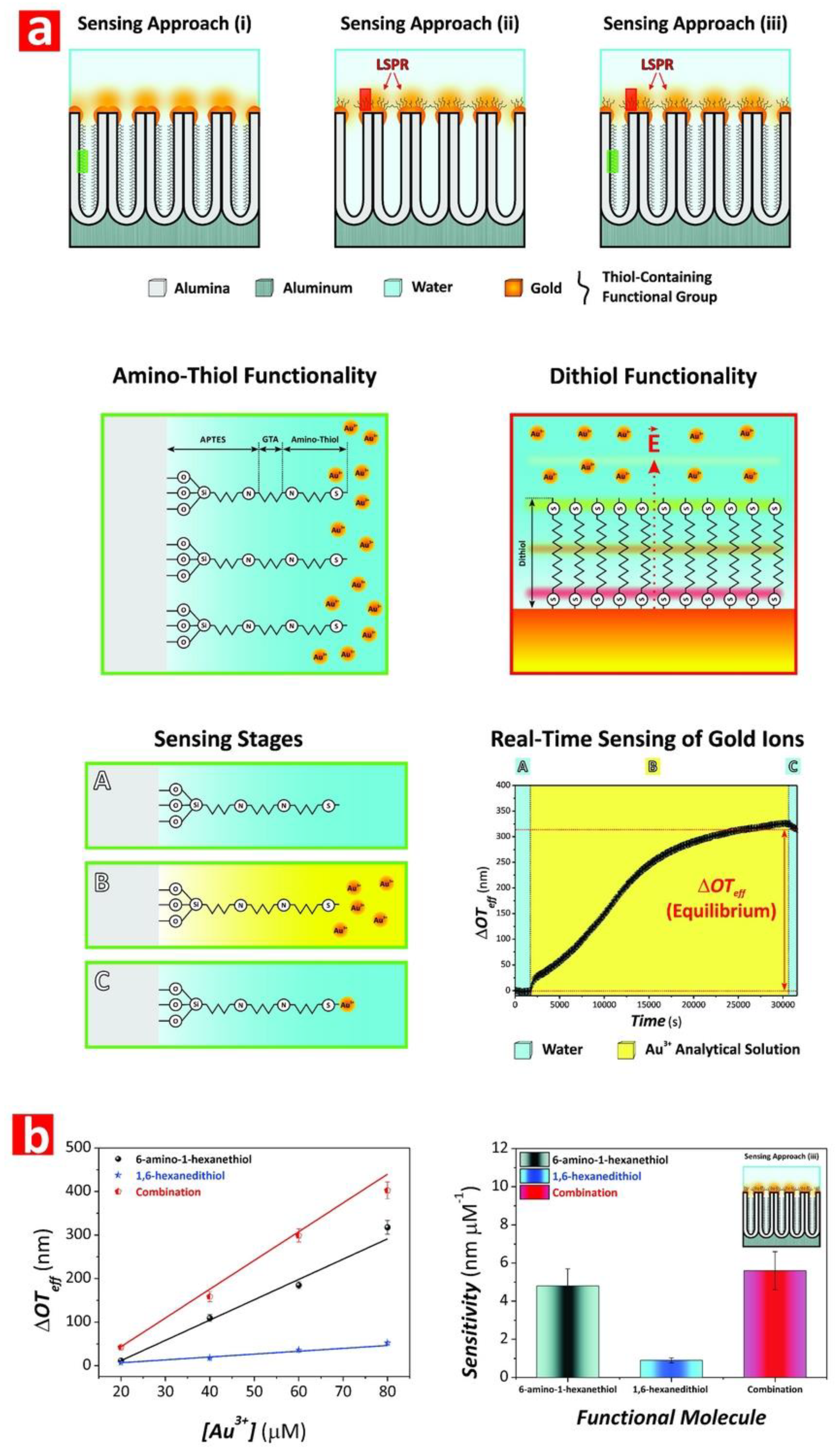
| [123] | NAA-FPI | Au3+ | RIfS | 5.6 nm µM−1 | |
| [240] | NAA-FPI | TNF-α | RIfS | 22.384 nm (ng mL−1)−1 | 0.13 μg mL−1 |
| [241] | NAA-FPI | Circulating tumour cells | RIfS | - | 1000 cells mL−1 |
| [232] | NAA-FPI | D-glucose | RIfS | 0.007% mM−1 | 100 mM |
| [43] | NAA-FPI | L-cysteine | RIfS | 0.026% mM−1 | 5 mM |
| [113] | NAA-FPI | Au3+ | RIfS | 1.09 nm µM−1 | 0.1 µM |
| [244] | NAA-FPI | Tyrypsin | RIfS | −106.9 nm (mg mL−1)−1 | 0.025 mg mL−1 |
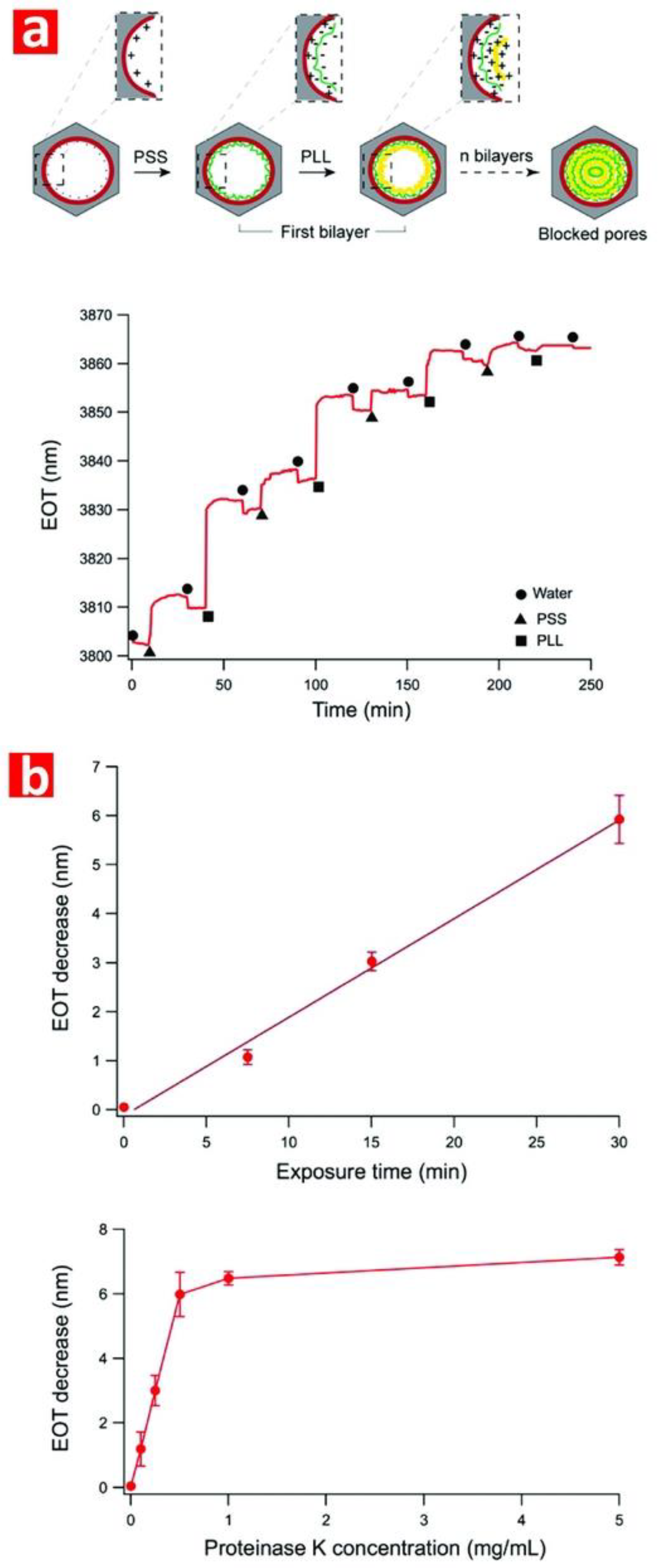
| [142] | NAA-FPI | Proteinase K | RIfS | 12.311 nm (mg mL−1)−1 | 0.06 mg mL−1 |
| [245] | NAA-FPI | β-galactosidase | RIfS | 39.04 nm (unit mL−1)−1 | 0.05 units enzyme mL−1 |
| [43] | NAA-FPI | D-glucose | PL | 0.013% mM−1 | 0.01 M |
| [43] | NAA-FPI | L-cysteine | PL | 0.029% mM−1 | 5 mM |
© 2018 by the authors. Licensee MDPI, Basel, Switzerland. This article is an open access article distributed under the terms and conditions of the Creative Commons Attribution (CC BY) license (http://creativecommons.org/licenses/by/4.0/).
Share and Cite
Law, C.S.; Lim, S.Y.; Abell, A.D.; Voelcker, N.H.; Santos, A. Nanoporous Anodic Alumina Photonic Crystals for Optical Chemo- and Biosensing: Fundamentals, Advances, and Perspectives. Nanomaterials 2018, 8, 788. https://doi.org/10.3390/nano8100788
Law CS, Lim SY, Abell AD, Voelcker NH, Santos A. Nanoporous Anodic Alumina Photonic Crystals for Optical Chemo- and Biosensing: Fundamentals, Advances, and Perspectives. Nanomaterials. 2018; 8(10):788. https://doi.org/10.3390/nano8100788
Chicago/Turabian StyleLaw, Cheryl Suwen, Siew Yee Lim, Andrew D. Abell, Nicolas H. Voelcker, and Abel Santos. 2018. "Nanoporous Anodic Alumina Photonic Crystals for Optical Chemo- and Biosensing: Fundamentals, Advances, and Perspectives" Nanomaterials 8, no. 10: 788. https://doi.org/10.3390/nano8100788